JP6012692B2 - Method for forming microlens array and method for manufacturing solid-state imaging device - Google Patents
Method for forming microlens array and method for manufacturing solid-state imaging device Download PDFInfo
- Publication number
- JP6012692B2 JP6012692B2 JP2014234005A JP2014234005A JP6012692B2 JP 6012692 B2 JP6012692 B2 JP 6012692B2 JP 2014234005 A JP2014234005 A JP 2014234005A JP 2014234005 A JP2014234005 A JP 2014234005A JP 6012692 B2 JP6012692 B2 JP 6012692B2
- Authority
- JP
- Japan
- Prior art keywords
- forming
- microlens
- microlens array
- shape
- etching
- Prior art date
- Legal status (The legal status is an assumption and is not a legal conclusion. Google has not performed a legal analysis and makes no representation as to the accuracy of the status listed.)
- Active
Links
- 238000000034 method Methods 0.000 title claims description 68
- 238000003384 imaging method Methods 0.000 title claims description 19
- 238000004519 manufacturing process Methods 0.000 title claims description 4
- 238000005530 etching Methods 0.000 claims description 54
- 238000000465 moulding Methods 0.000 claims description 19
- 239000000463 material Substances 0.000 claims description 10
- 238000006243 chemical reaction Methods 0.000 claims description 9
- 239000011347 resin Substances 0.000 claims description 7
- 229920005989 resin Polymers 0.000 claims description 7
- PPBRXRYQALVLMV-UHFFFAOYSA-N Styrene Chemical compound C=CC1=CC=CC=C1 PPBRXRYQALVLMV-UHFFFAOYSA-N 0.000 claims description 6
- 239000000758 substrate Substances 0.000 claims description 6
- 230000002093 peripheral effect Effects 0.000 claims description 4
- 239000004925 Acrylic resin Substances 0.000 claims description 2
- 229920000178 Acrylic resin Polymers 0.000 claims description 2
- 238000002834 transmittance Methods 0.000 description 15
- 238000009826 distribution Methods 0.000 description 13
- 230000015572 biosynthetic process Effects 0.000 description 9
- 238000010586 diagram Methods 0.000 description 7
- WGTYBPLFGIVFAS-UHFFFAOYSA-M tetramethylammonium hydroxide Chemical compound [OH-].C[N+](C)(C)C WGTYBPLFGIVFAS-UHFFFAOYSA-M 0.000 description 4
- 239000011159 matrix material Substances 0.000 description 3
- 230000001419 dependent effect Effects 0.000 description 2
- 230000000694 effects Effects 0.000 description 2
- 230000010354 integration Effects 0.000 description 2
- 230000001788 irregular Effects 0.000 description 2
- 229920002120 photoresistant polymer Polymers 0.000 description 2
- 238000004528 spin coating Methods 0.000 description 2
- 206010034972 Photosensitivity reaction Diseases 0.000 description 1
- 229910052581 Si3N4 Inorganic materials 0.000 description 1
- VYPSYNLAJGMNEJ-UHFFFAOYSA-N Silicium dioxide Chemical compound O=[Si]=O VYPSYNLAJGMNEJ-UHFFFAOYSA-N 0.000 description 1
- 238000004061 bleaching Methods 0.000 description 1
- 229910010272 inorganic material Inorganic materials 0.000 description 1
- 239000011147 inorganic material Substances 0.000 description 1
- 238000002156 mixing Methods 0.000 description 1
- 230000003287 optical effect Effects 0.000 description 1
- 239000002245 particle Substances 0.000 description 1
- 238000000059 patterning Methods 0.000 description 1
- 230000035699 permeability Effects 0.000 description 1
- 230000036211 photosensitivity Effects 0.000 description 1
- 239000004065 semiconductor Substances 0.000 description 1
- HQVNEWCFYHHQES-UHFFFAOYSA-N silicon nitride Chemical compound N12[Si]34N5[Si]62N3[Si]51N64 HQVNEWCFYHHQES-UHFFFAOYSA-N 0.000 description 1
- 229910052814 silicon oxide Inorganic materials 0.000 description 1
Images


Classifications
-
- H—ELECTRICITY
- H01—ELECTRIC ELEMENTS
- H01L—SEMICONDUCTOR DEVICES NOT COVERED BY CLASS H10
- H01L27/00—Devices consisting of a plurality of semiconductor or other solid-state components formed in or on a common substrate
- H01L27/14—Devices consisting of a plurality of semiconductor or other solid-state components formed in or on a common substrate including semiconductor components sensitive to infrared radiation, light, electromagnetic radiation of shorter wavelength or corpuscular radiation and specially adapted either for the conversion of the energy of such radiation into electrical energy or for the control of electrical energy by such radiation
- H01L27/144—Devices controlled by radiation
- H01L27/146—Imager structures
- H01L27/14683—Processes or apparatus peculiar to the manufacture or treatment of these devices or parts thereof
- H01L27/14685—Process for coatings or optical elements
-
- B—PERFORMING OPERATIONS; TRANSPORTING
- B29—WORKING OF PLASTICS; WORKING OF SUBSTANCES IN A PLASTIC STATE IN GENERAL
- B29D—PRODUCING PARTICULAR ARTICLES FROM PLASTICS OR FROM SUBSTANCES IN A PLASTIC STATE
- B29D11/00—Producing optical elements, e.g. lenses or prisms
- B29D11/00009—Production of simple or compound lenses
- B29D11/00278—Lenticular sheets
- B29D11/00298—Producing lens arrays
-
- B—PERFORMING OPERATIONS; TRANSPORTING
- B29—WORKING OF PLASTICS; WORKING OF SUBSTANCES IN A PLASTIC STATE IN GENERAL
- B29D—PRODUCING PARTICULAR ARTICLES FROM PLASTICS OR FROM SUBSTANCES IN A PLASTIC STATE
- B29D11/00—Producing optical elements, e.g. lenses or prisms
- B29D11/00009—Production of simple or compound lenses
- B29D11/00365—Production of microlenses
-
- G—PHYSICS
- G02—OPTICS
- G02B—OPTICAL ELEMENTS, SYSTEMS OR APPARATUS
- G02B3/00—Simple or compound lenses
- G02B3/0006—Arrays
- G02B3/0012—Arrays characterised by the manufacturing method
- G02B3/0018—Reflow, i.e. characterized by the step of melting microstructures to form curved surfaces, e.g. manufacturing of moulds and surfaces for transfer etching
-
- G—PHYSICS
- G02—OPTICS
- G02B—OPTICAL ELEMENTS, SYSTEMS OR APPARATUS
- G02B3/00—Simple or compound lenses
- G02B3/0006—Arrays
- G02B3/0037—Arrays characterized by the distribution or form of lenses
- G02B3/0043—Inhomogeneous or irregular arrays, e.g. varying shape, size, height
-
- H—ELECTRICITY
- H01—ELECTRIC ELEMENTS
- H01L—SEMICONDUCTOR DEVICES NOT COVERED BY CLASS H10
- H01L27/00—Devices consisting of a plurality of semiconductor or other solid-state components formed in or on a common substrate
- H01L27/14—Devices consisting of a plurality of semiconductor or other solid-state components formed in or on a common substrate including semiconductor components sensitive to infrared radiation, light, electromagnetic radiation of shorter wavelength or corpuscular radiation and specially adapted either for the conversion of the energy of such radiation into electrical energy or for the control of electrical energy by such radiation
- H01L27/144—Devices controlled by radiation
- H01L27/146—Imager structures
- H01L27/14601—Structural or functional details thereof
- H01L27/14625—Optical elements or arrangements associated with the device
- H01L27/14627—Microlenses
Landscapes
- Physics & Mathematics (AREA)
- Engineering & Computer Science (AREA)
- General Physics & Mathematics (AREA)
- Power Engineering (AREA)
- Manufacturing & Machinery (AREA)
- Optics & Photonics (AREA)
- Microelectronics & Electronic Packaging (AREA)
- Computer Hardware Design (AREA)
- Condensed Matter Physics & Semiconductors (AREA)
- Electromagnetism (AREA)
- Chemical & Material Sciences (AREA)
- Crystallography & Structural Chemistry (AREA)
- Health & Medical Sciences (AREA)
- Ophthalmology & Optometry (AREA)
- Mechanical Engineering (AREA)
- Solid State Image Pick-Up Elements (AREA)
- Transforming Light Signals Into Electric Signals (AREA)
Description
本発明は、マイクロレンズの形成方法および固体撮像素子の製造方法に関する。 The present invention relates to a method for forming a microlens and a method for manufacturing a solid-state imaging device.
特許文献1には、マイクロレンズの形成方法が開示されている。具体的には、まず、平坦な透光性部材の上に複数のレンズパターンを形成する。該複数のレンズパターンは、透光性部材の上に形成されたレンズ部材のパターニングおよびリフローを行うことにより形成され、隣接レンズパターン間にはギャップが存在する。その後、透光性部材のうちのレンズパターン間のギャップにより露出した部分を、複数のレンズパターンをマスクとしてエッチングし、透光性部材の該レンズパターン間の領域に凹部形状(溝)を形成する。
この方法によると、凹部形状が形成された透光性部材とレンズパターンとにより、隣接マイクロレンズ間にギャップのないマイクロレンズアレイが形成される。 According to this method, a microlens array having no gap between adjacent microlenses is formed by the translucent member having the concave shape and the lens pattern.
特許文献1の方法によると、上記透光性部材の凹部形状は、透光性部材のうちのレンズパターンにより当初からレンズ間ギャップ部により露出している部分のみをエッチングで除去して形成される。そのため、この方法では、該凹部形状を任意に制御することができず、該凹部形状を含むマイクロレンズ全体の形状を制御することが難しい。
According to the method of
本発明は、マイクロレンズの形状を制御するのに有利な技術を提供することを目的とする。 An object of the present invention is to provide a technique advantageous for controlling the shape of a microlens.
本発明の一つの側面はマイクロレンズアレイの形成方法にかかり、前記マイクロレンズアレイの形成方法は、複数のマイクロレンズがアレイ状に形成されたマイクロレンズアレイであって前記複数のマイクロレンズの少なくとも一部が非対称な形状を有するマイクロレンズアレイを形成する方法であって、第1の部材の上に、該第1の部材とは異なる材料からなる第2の部材を形成する第1工程と、グレースケールマスクであるフォトマスクを用いて前記第2の部材を露光して現像することにより、前記第2の部材を、その上面が、複数の凸部と複数の凹部とを有する凹凸形状を有するように成形する第2工程と、前記成形された前記第2の部材と前記第1の部材とをエッチングすることにより、少なくとも前記第1の部材から、前記複数の凸部に対応する前記複数のマイクロレンズを形成する第3工程と、を有し、前記第2工程で形成された前記複数の凸部は、第1の凸部と、前記第1の凸部と対辺方向において隣り合う第2の凸部と、前記第1の凸部と対角方向において隣り合う第3の凸部と、を含み、前記第2工程では、前記第1の部材の一部であって前記複数の凹部のうちの前記第1の凸部と前記第3の凸部との間の凹部の下に位置する一部が露出され、前記第3工程では、前記第1の部材のエッチングレートが前記第2の部材のエッチングレートよりも大きい条件で、前記第2の部材のエッチングと前記第1の部材のエッチングとを行うことを特徴とする。
One aspect of the present invention relates to a method of forming a microlens array, the method of forming a microlens array, at least one of the plurality of micro lenses wherein the plurality of micro lenses to a microlens array formed in an array A method of forming a microlens array having an asymmetrical portion, a first step of forming a second member made of a material different from the first member on the first member; by developing by exposing the pre-Symbol second member by using a photomask is scale mask, the second member, the upper surface of that is, an uneven shape having a plurality of projections and a plurality of recesses a second step of molding so as to have, by etching with said first member and said second member to which the molded, from at least the first member, the plurality of A third step of forming the plurality of microlenses corresponding to section, wherein the plurality of convex portions formed in the second step, a first protrusion, said first protrusion A second convex portion adjacent in the opposite direction, and a third convex portion adjacent in the diagonal direction to the first convex portion, and in the second step, a part of the first member In the third step, a part of the plurality of concave portions located under the concave portion between the first convex portion and the third convex portion is exposed, and in the third step, in larger conditions than the etching rate of the etching rate is the second member, characterized in that intends rows and etching said etching of the second member first member.
本発明によれば、マイクロレンズの形状を制御するのに有利である。 The present invention is advantageous for controlling the shape of the microlens.
(第1実施形態)
図1〜3を参照しながら第1実施形態を説明する。
(First embodiment)
The first embodiment will be described with reference to FIGS.
図1は、マイクロレンズアレイAMLを説明するための模式図(平面視)である。マイクロレンズアレイAMLは、複数のマイクロレンズがアレイ状に配列されて形成され、ここでは、説明を容易にするため、3行×3列のマイクロレンズアレイAMLを示している。図中において、実線は、単位マイクロレンズ領域RMLを示しており、破線は、マイクロレンズの凸部を示している。 FIG. 1 is a schematic diagram (plan view) for explaining the microlens array A ML . The microlens array A ML is formed by arranging a plurality of microlenses in an array. Here, for ease of explanation, the microlens array AML is shown as a 3 × 3 microlens array AML . In the figure, the solid line indicates the unit microlens region RML , and the broken line indicates the convex portion of the microlens.
なお、本明細書において、図中のA−A’方向を「対辺方向」と称し、B−B’方向を「対角方向」と称する。図1に示された複数(ここでは9つ)のマイクロレンズの凸部のうち、注目すべき真ん中の凸部を「第1の凸部」と称する。第1の凸部の周囲には凹部が存在する。この例では凸部の全周が凹部で囲まれている。対辺方向(図中の上下左右方向)において、第1の凸部に凹部を介して隣り合う4つの凸部を「第2の凸部」と称する。対角方向(図中の斜め方向)において、第1の凸部に凹部を介して隣り合う4つの凸部を「第3の凸部」と称する。即ち、第3の凸部の頂は、第2の凸部の頂よりも第1の凸部の頂から遠い位置であり、第1の凸部の頂と第2の凸部の頂との距離をPとすると、第1の凸部の頂と第2の凸部の頂との距離は、例えばP×21/2である。 In the present specification, the AA ′ direction in the drawing is referred to as “the opposite direction”, and the BB ′ direction is referred to as “the diagonal direction”. Of the plurality of (here, nine) microlens convex portions shown in FIG. 1, the middle convex portion to be noted is referred to as a “first convex portion”. A concave portion exists around the first convex portion. In this example, the entire circumference of the convex portion is surrounded by the concave portion. In the opposite direction (up / down / left / right direction in the figure), the four convex portions adjacent to the first convex portion via the concave portion are referred to as “second convex portions”. In the diagonal direction (oblique direction in the figure), the four convex portions adjacent to the first convex portion via the concave portion are referred to as “third convex portions”. That is, the top of the third convex portion is a position farther from the top of the first convex portion than the top of the second convex portion, and the top of the first convex portion and the top of the second convex portion. If the distance is P, the distance between the top of the first convex portion and the top of the second convex portion is, for example, P × 2½ .
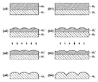
図2は、本実施形態にかかるマイクロレンズの形成方法を工程ごとに説明するための模式図である。図2(a1)〜(a4)は、対辺方向における各工程の態様を示している。図2(b1)〜(b4)は、図2(a1)〜(a4)に対応する各工程の対角方向における態様を、それぞれ示している。 FIG. 2 is a schematic diagram for explaining the microlens forming method according to the present embodiment for each step. FIGS. 2A1 to 2A4 show the mode of each process in the opposite direction. 2 (b1) to 2 (b4) respectively show aspects in the diagonal direction of the respective steps corresponding to FIGS. 2 (a1) to (a4).
まず、図2(a1)及び(b1)に示されるように、マイクロレンズを形成するための第1の部材M1の上に、該部材M1とは異なる第2の部材M2を形成する。部材M1は、例えば、所定の半導体素子等が形成された基板の上に、スピンコート法(及び、ベーク処理:230℃・6分)等により成膜される。部材M1の材料には、例えば、アクリル系樹脂が用いられうる。部材M2は、部材M1の上に、スピンコート法(及び、ベーク処理:110℃・1.5分)等により成膜される。部材M2の材料には、例えば、スチレン系樹脂が用いられうる。このように、部材M1としての樹脂層と部材M2としての樹脂層との積層膜である樹脂膜が得られる。部材M1及び部材M2の材料は、上述の樹脂材料以外のものが用いられてもよいし、酸化シリコンや窒化シリコン等の無機材料が用いられてもよい。 First, as shown in FIG. 2 (a1) and (b1), on the first member M 1 for forming a microlens, to form a different second member M 2 and the member M 1 . Member M 1 is, for example, on a substrate such as a predetermined semiconductor element is formed, a spin coating method (and baked: 230 ° C. · 6 minutes) is deposited by like. The material of the members M 1, for example, acrylic resin may be used. Member M 2 is on the member M 1, a spin coating method (and baked: 110 ° C. · 1.5 minutes) is deposited by like. The material of the member M 2, for example, styrene-based resins may be used. Thus, the resin film can be obtained a laminated film of a resin layer as the resin layer and the member M 2 as member M 1. As the material of the member M 1 and the member M 2 , materials other than the above-described resin materials may be used, or inorganic materials such as silicon oxide and silicon nitride may be used.
次に、図2(a2)及び(b2)に示されるように、部材M2を、その上面が凹凸形状を有するように成形する。成形された部材M2を「M2’」で示す。部材M2’は、複数の凸部と、該複数の凸部の間の凹部を有する。部材M2’の上面の凹凸形状は、この凸部と、凸部の周囲の凹部とによって形成される。ここでは、凸部の全周が凹部で囲まれており、部材M1の上面の全面が部材M2’で覆われている例を示した。仮に、部材M1の上面の全部が部材M2’で覆われていないと、部材M2’をマスクとして用いて部材M1をエッチングする際に、部材M1に形成されるパターンが、部材M1の上面の露出部の形状に依存して決まってしまう。そうすると、部材M2’の形状が部材M1に十分反映されず、所望の形状を有するマイクロレンズを形成できなくなる。したがって、上記凹部において、部材M1の上面の少なくとも一部が部材M2’で覆われていることが好ましい。その一方で、凸部の周囲の一部に部材M2’の凹部が存在せずに、一部の部材M1が露出している構成例も本発明は包含しうる。より具体的には、B−B’方向である対角方向については部材M1の上面が露出しているが、A−A´方向である対辺方向については部材M1の上面が露出していない構成例も本発明に包含される。 Next, as shown in FIG. 2 (a2) and (b2), the member M 2, its upper surface is shaped to have an irregular shape. The molded member M 2 is indicated by “M 2 ′”. The member M 2 ′ has a plurality of protrusions and a recess between the plurality of protrusions. The concavo-convex shape on the upper surface of the member M 2 ′ is formed by the convex portions and the concave portions around the convex portions. Here, an example is shown in which the entire circumference of the convex portion is surrounded by the concave portion, and the entire upper surface of the member M1 is covered with the member M 2 ′. If, 'if not covered, the member M 2' entire upper surface of the member M1 is member M 2 when the member M1 is etched using as a mask, the pattern formed on the member M1, the upper surface of the member M1 It depends on the shape of the exposed part. As a result, the shape of the member M 2 ′ is not sufficiently reflected on the member M1, and a microlens having a desired shape cannot be formed. Therefore, in the recess, at least a part of the upper surface of the member M1 is preferably covered with the member M 2 ′. On the other hand, the present invention can also include a configuration example in which a part of the member M1 is exposed without the concave part of the member M 2 ′ being part of the periphery of the convex part. More specifically, the upper surface of the member M1 is exposed in the diagonal direction that is the BB ′ direction, but the upper surface of the member M1 is not exposed in the opposite direction that is the AA ′ direction. Examples are also encompassed by the present invention.
部材M2’は、上記マイクロレンズアレイAMLにおける複数の凸部に対応する第1〜3の凸部を有する。この工程を「第1の成形工程」と称する。この工程は、例えば、フォトマスクを用いて部材M2を露光した後、これを現像することによってなされうる。本実施形態では、フォトマスクとしてグレースケールマスクを用いた。また、露光量を2000〜2700J/m2とした。また、現像液にはTMAH(テトラメチルアンモニウムヒドロキシド)2.38%を用い、現像時間を45秒とした。なお、この工程は、ポジ型およびネガ型のいずれの態様でも可能である。 The member M 2 ′ has first to third protrusions corresponding to the plurality of protrusions in the microlens array A ML . This process is referred to as a “first molding process”. This step may, for example, after exposing the member M 2 using a photomask may be made by developing it. In this embodiment, a gray scale mask is used as a photomask. The exposure amount was 2000~2700J / m 2. Further, TMAH (tetramethylammonium hydroxide) 2.38% was used as the developer, and the development time was 45 seconds. This step can be performed in either a positive type or a negative type.
グレースケールマスクは、露光光の透過率分布を有する多階調マスクである。透過率分布は、例えば、遮光体の厚みの分布や、微細なドット状の遮光体の粗密の分布によって形成される。例えばポジ型の態様を考えた場合、単位マイクロレンズ領域における中央領域(即ち、マイクロレンズの凸部となるべき領域)では露光光の透過率が低く、周辺領域(凹部となるべき領域)では露光光の透過率が高い。よって、現像後には、透過率の低い(露光光量の少ない)中央領域には部材M2’の凸部が形成され、透過率の高い(露光光量の多い)周辺領域には部材M2’の凹部が形成される。後に詳細を述べるが、この形成方法によると、部材M2を例えばリフロー法によってレンズ形状に成形する場合に比べて、その形状を制御するのに有利である。 The gray scale mask is a multi-tone mask having a transmittance distribution of exposure light. The transmittance distribution is formed by, for example, the thickness distribution of the light shielding body or the coarse and dense distribution of fine dot-shaped light shielding bodies. For example, when considering a positive mode, exposure light transmittance is low in the central region of the unit microlens region (that is, the region that should be the convex portion of the microlens), and exposure is performed in the peripheral region (the region that should be the concave portion). High light transmittance. Therefore, after the development, the convex portion of the member M 2 ′ is formed in the central region where the transmittance is low (the amount of exposure light is small), and in the peripheral region where the transmittance is high (the amount of exposure light is large) of the member M 2 ′. A recess is formed. Although described in detail later, according to this forming method, as compared with the case of molding the member M 2 into a lens shape, for example, by a reflow method, it is advantageous to control the shape.
なお、現像後には、成形された(上面に凹凸形状が形成された)部材M2’のブリーチング(露光量12000J/m2)およびベーク処理(125℃・5分、140℃・5分、200℃・5分)がなされうる。 After development, bleaching (exposure amount: 12000 J / m 2 ) and baking treatment (125 ° C./5 minutes, 140 ° C./5 minutes) of the molded member M 2 ′ (with an uneven shape formed on the upper surface), 200 ° C., 5 minutes).
その後、成形された部材M2’と部材M1の一部とをエッチングして、部材MLを成形する。この工程を「第2の成形工程」と称する。この工程により、複数のマイクロレンズMLによるマイクロレンズアレイAMLが形成される。 Thereafter, the formed member M 2 ′ and a part of the member M 1 are etched to form the member ML. This process is referred to as a “second molding process”. By this step, a microlens array A ML is formed by a plurality of microlenses ML.
図2(a3)及び(b3)は、部材M2のエッチング中の様子を示している。 Figure 2 (a3) and (b3) shows the state during the etching of the member M 2.
エッチング条件は、
RF電力:1400W
圧力:40mT
C4F8:10sccm
CF4:110sccm
エッチング時間:300秒
とした。
Etching conditions are
RF power: 1400W
Pressure: 40mT
C 4 F 8 : 10 sccm
CF 4 : 110 sccm
Etching time: 300 seconds.
図2(a4)及び(b4)は、部材M1の一部のエッチングが完了した後の様子を示している。上記エッチングにより、部材M2’の凹凸形状が部材M1に転写され、部材M2’の凸部に対応するマイクロレンズMLを有するマイクロレンズアレイAMLが形成される。 Figure 2 (a4) and (b4) shows the state after a part of the etching of the member M 1 is completed. By the etching, the uneven shape of the member M 2 ′ is transferred to the member M 1 , and the micro lens array A ML having the micro lens ML corresponding to the convex portion of the member M 2 ′ is formed.
ここで、上記エッチングは、部材M1のエッチングレートが部材M2’(M2)のエッチングレートよりも大きい条件でなされる。本実施形態では、部材M1のエッチングレートを60Å/秒とし、部材M2’のエッチングレートを45Å/秒とした。 Here, the etching is performed under the condition that the etching rate of the member M 1 is larger than the etching rate of the member M 2 ′ (M 2 ). In the present embodiment, the etching rate of the member M 1 is 60 Å / second, and the etching rate of the member M 2 ′ is 45 Å / second.
上記エッチングレートの場合、部材M1と部材M2’とのエッチングレート比は4/3である。よって、例えば、部材M2’の凹凸形状の高低差(凸部と凹部との高低差)をHとしたとき、第2の成形工程後の(一部がエッチングされた)部材M1の凹凸形状の高低差は、略H×4/3となる。 In the case of the above etching rate, the etching rate ratio between the member M 1 and the member M 2 ′ is 4/3. Therefore, for example, when the height difference of the concavo-convex shape of the member M 2 ′ (height difference between the convex portion and the concave portion) is H, the concavo-convex portion of the member M 1 (partially etched) after the second forming step. The difference in shape is approximately H × 4/3.
具体的には、上記エッチングでは、まず、部材M2’の凹部で部材M1の上面の一部分が露出する。例えば、部材M2’の凹凸形状の、対辺方向での曲率と、対角方向での曲率とが互いに等しい場合には、まず、対角方向における凹部(前述の第1の凸部と第3の凸部の間の部分)で部材M1の上面が露出する。その後、対辺方向における凹部(前述の第1の凸部と第2の凸部の間の部分)で部材M1の上面が露出する。さらにその後、部材M2’の凸部がエッチングされると共に、部材M1の該露出した一部分がエッチングによって除去される。 Specifically, in the above etching, first, a portion of the upper surface of the member M 1 in the recess of the member M 2 'is exposed. For example, when the curvature in the opposite direction and the curvature in the diagonal direction of the concavo-convex shape of the member M 2 ′ are equal to each other, first, the concave portions in the diagonal direction (the first convex portion and the third the upper surface of the member M 1 in part) between the convex portion is exposed. Thereafter, the upper surface of the member M 1 by (part between the first protrusion and second protrusion above) the recess in the opposite side direction is exposed. Thereafter, the protrusion of the member M 2 ′ is etched and the exposed part of the member M 1 is removed by etching.
よって、この形成方法によると、部材M1の凹凸形状の高低差は、部材M2’の凹凸形状の高低差よりも大きくなる。他の観点では、部材M1は、部材M2’の凹凸形状の曲率よりも大きい曲率の凹凸形状に成形される。換言すると、この形成方法によると、部材M1の上面には、部材M2’の凹凸形状を強調した凹凸形状が形成される。 Therefore, according to this forming method, the height difference of the uneven shape of the member M 1 becomes larger than the height difference of the uneven shape of the member M 2 ′. From another point of view, the member M 1 is formed into a concavo-convex shape having a larger curvature than that of the concavo-convex shape of the member M 2 ′. In other words, according to this forming method, an uneven shape that emphasizes the uneven shape of the member M 2 ′ is formed on the upper surface of the member M 1 .
前述のとおり、上記エッチングは、部材M1のエッチングレートが部材M2’のエッチングレートよりも大きい条件でなされる。該エッチングによると、対辺方向および対角方向のいずれにおいても、部材M1の凹部(即ち、隣接マイクロレンズML間の境界部分の形状)が、部材M2’の凹部よりも鋭角になる。その結果、隣接マイクロレンズML間での距離が小さい、いわゆるギャップレスのマイクロレンズアレイAMLが形成される。 As described above, the etching is performed under the condition that the etching rate of the member M 1 is larger than the etching rate of the member M 2 ′. According to the etching, the concave portion of the member M 1 (that is, the shape of the boundary portion between the adjacent microlenses ML) becomes sharper than the concave portion of the member M 2 ′ in both the opposite direction and the diagonal direction. As a result, a so-called gapless microlens array AML having a small distance between adjacent microlenses ML is formed.
以上の形成方法によると、マイクロレンズMLの形状は、部材M2’の形状と、部材M1と部材M2’とのエッチングレート比と、に依存する。よって、マイクロレンズMLを所望の形状に形成するためには、第1の成形工程での部材M2’の凹凸形状の形成の制御と、第2の成形工程での部材M1および部材M2’のエッチングレートの設定と、が適切になされればよい。 According to the above forming method, the shape of the microlenses ML is dependent 'and the shape of, member M 1 and the member M 2' member M 2 and the etching rate ratio between, on. Therefore, in order to form the microlens ML in a desired shape, the control of the formation of the concavo-convex shape of the member M 2 ′ in the first molding step and the members M 1 and M 2 in the second molding step are performed. It is only necessary to properly set the etching rate.
まとめると、第1の成形工程は、フォトマスクとしてグレースケールマスクを用いて露光処理を行い、その後、現像処理を行うことによってなされうる。その後の第2の成形工程は、部材M1のエッチングレートが部材M2’のエッチングレートよりも大きい条件でなされる。よって、本形成方法によると、マイクロレンズMLの形成の際、即ち、部材M2’の凹凸形状を部材M1に転写する際に、部材M1と部材M2’とのエッチングレート比により、該部材M2’の凹凸形状の高低差よりも大きい高低差の凹凸形状が部材M1に形成される。他の観点では、本形成方法によると、使用するグレースケールマスクの解像度よりも高い解像度でマイクロレンズの形状を制御することが可能である。 In summary, the first forming step can be performed by performing an exposure process using a gray scale mask as a photomask and then performing a development process. The subsequent second forming step is performed under the condition that the etching rate of the member M 1 is larger than the etching rate of the member M 2 ′. Therefore, according to this forming method, the formation of the microlenses ML, i.e., 'when transferring the uneven shape of the member M 1, member M 1 and the member M 2' member M 2 by the etching rate ratio between, An uneven shape having a height difference larger than the height difference of the uneven shape of the member M 2 ′ is formed on the member M 1 . From another viewpoint, according to the present forming method, the shape of the microlens can be controlled with a resolution higher than that of the grayscale mask to be used.
また、マイクロレンズMLの形状は、第1の成形工程での部材M2’の凹凸形状にしたがうため、マイクロレンズMLの形状を任意の形状に制御することが可能である。よって、本形成方法によると、例えば、ギャップレスのマイクロレンズアレイAMLを形成するのにも有利である。また、マイクロレンズMLの形状を高い精度で制御するため、部材M1と部材M2’とのエッチングレート比を、部材M1のエッチングレートと部材M2’のエッチングレートとの差が、例えば5Å/秒から50Å/秒の範囲内となるように設定するとよい。 Moreover, since the shape of the microlens ML follows the uneven shape of the member M 2 ′ in the first molding step, the shape of the microlens ML can be controlled to an arbitrary shape. Accordingly, with the present forming method, for example, it is advantageous to form the microlens array A ML gapless. In order to control the shape of the microlens ML with high accuracy, 'the etching rate ratio between the etching rate and the member M 2 of element M 1' member M 1 and the member M 2 is a difference between the etching rate of, for example, It may be set to be in the range of 5 Å / second to 50 Å / second.
図3は、対辺方向におけるマイクロレンズアレイAMLの断面形状を説明するための模式図である。単位マイクロレンズ領域RML(図1参照)は、第1領域R1(中央領域)と、第2領域R2(周辺領域)とに分けられる。領域R1は、例えば、マイクロレンズMLの上面が凸形状となる第1の曲率を有する領域である。領域R2は、例えば、マイクロレンズMLの上面が凹形状となる第2の曲率を有する領域である。他の観点では、領域R1と領域R2との境界は、マイクロレンズMLの上面形状の変曲点によって形成されうる。図1に示した破線は、凸部の外縁ないし輪郭を示しており、また、領域R1と領域2の境界に対応する。
FIG. 3 is a schematic diagram for explaining a cross-sectional shape of the microlens array A ML in the opposite side direction. The unit microlens region R ML (see FIG. 1) is divided into a first region R1 (central region) and a second region R2 (peripheral region). The region R1 is, for example, a region having a first curvature where the upper surface of the microlens ML has a convex shape. The region R2 is, for example, a region having a second curvature in which the upper surface of the microlens ML has a concave shape. In another aspect, the boundary between the region R1 and the region R2 can be formed by an inflection point of the upper surface shape of the microlens ML. The broken line shown in FIG. 1 indicates the outer edge or outline of the convex portion, and corresponds to the boundary between the region R1 and the
例えば、あるマイクロレンズ(MLAとする)の領域R1と、該マイクロレンズMLAに隣接するマイクロレンズ(MLBとする)の領域R1との距離は、マイクロレンズMLのピッチ(配列間隔)の10分の1より小さいとよい。これにより、集光率の高いギャップレスのマイクロレンズアレイAMLが得られる。 For example, the distance between a region R1 of a certain micro lens (referred to as ML A ) and a region R1 of a micro lens (referred to as ML B ) adjacent to the micro lens ML A is equal to the pitch (arrangement interval) of the micro lenses ML. It is better to be smaller than 1/10. As a result, a gapless microlens array A ML having a high light collection rate is obtained.
ここで、領域R1では、マイクロレンズMLの上面が球面形状(断面が円弧の形状)を形成しているとよい。これにより、マイクロレンズMLを、例えばCMOSセンサ等の固体撮像素子に適用する場合には、光感度やF値(Fno)比例性が向上し、センサ性能が向上する。 Here, in the region R1, it is preferable that the upper surface of the microlens ML has a spherical shape (the cross section has an arc shape). Thereby, when the microlens ML is applied to a solid-state imaging device such as a CMOS sensor, for example, the photosensitivity and F value (Fno) proportionality are improved, and the sensor performance is improved.
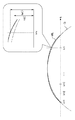
以下、図4を参照しながら、マイクロレンズMLの球面形状について述べる。図4は、領域R1のマイクロレンズMLの形状と、理想的な真球(いずれの断面においても真円となる球体)との一致率を説明するための模式図である。理想的な真球は、マイクロレンズMLの頂に重なり、且つ、領域R1の外縁に重なる球Ciを想定する。 Hereinafter, the spherical shape of the microlens ML will be described with reference to FIG. FIG. 4 is a schematic diagram for explaining the coincidence ratio between the shape of the microlens ML in the region R1 and an ideal true sphere (a sphere that is a perfect circle in any cross section). An ideal sphere is assumed to be a sphere Ci that overlaps the top of the microlens ML and overlaps the outer edge of the region R1.
次に、領域R1を所定数のマトリクス(所定の行数×所定の列数)に分割する。マトリクスの各格子点i(i=1〜n)での、マイクロレンズMLの高さをhr(i)とし、理想的な真球Ciの高さをhi(i)とする。なお、nは、2以上の整数であり、分割したマトリクス上の格子点の数である。また、「高さ」は、領域R1の外縁の位置を基準とする高さとする。 Next, the region R1 is divided into a predetermined number of matrices (a predetermined number of rows × a predetermined number of columns). The height of the microlens ML at each lattice point i (i = 1 to n) of the matrix is set to hr (i), and the height of the ideal sphere Ci is set to hi (i). Note that n is an integer of 2 or more and is the number of lattice points on the divided matrix. The “height” is a height based on the position of the outer edge of the region R1.
ここで、Δh(i)≡|hr(i)―hi(i)|としたときに、
上記一致率を、
一致率RM≡(1−ΣΔh(i)/Σhi(i))×100[%]、
と定義する(Σは、i=1〜nでの総和)。
Here, when Δh (i) ≡ | hr (i) −hi (i) |
The above match rate is
Match rate R M ≡ (1-ΣΔh (i) / Σhi (i)) × 100 [%],
(Σ is the sum of i = 1 to n).
この定義において、例えば41行×41列のマトリクス(n=41×41)で一致率RMを算出したとき、例えばRM≧85%であれば、マイクロレンズMLは良好な球面形状を有すると言える。 In this definition, for example, when the coincidence rate R M is calculated with a matrix of 41 rows × 41 columns (n = 41 × 41), for example, if R M ≧ 85%, the microlens ML has a good spherical shape. I can say that.
前述のとおり、本実施形態の形成方法によると、マイクロレンズMLの形状は、部材M2’の形状と、部材M1と部材M2’とのエッチングレート比と、に依存する。そのため、所望の球面形状を有するマイクロレンズMLが形成されるように、予め、第1の成形工程および第2の成形工程の条件を選択すればよい。具体的には、露光条件の設定、及び、形成されるべき部材M2’の凹凸形状を形成するためのグレースケールマスクの準備、並びに、上記エッチングレート比の選択がなされればよい。 As described above, according to the forming method of this embodiment, the shape of the microlens ML is dependent 'and the shape of, member M 1 and the member M 2' member M 2 and the etching rate ratio between, on. Therefore, the conditions of the first molding step and the second molding step may be selected in advance so that the microlens ML having a desired spherical shape is formed. Specifically, it is only necessary to set exposure conditions, prepare a gray scale mask for forming the uneven shape of the member M 2 ′ to be formed, and select the etching rate ratio.
以上、本実施形態によると、マイクロレンズMLの形状の制御、ギャップレスのマイクロレンズアレイAMLの形成、及び、マイクロレンズアレイAMLの高集積化に有利である。 As described above, according to this embodiment, it is advantageous for controlling the shape of the microlens ML , forming the gapless microlens array AML, and highly integrating the microlens array AML .
例えば、複数のレンズパターンをリフロー法で形成する場合には、隣接レンズパターンが接触しないように、隣接レンズパターン間には所定のギャップを設ける必要がある。一方で、本実施形態によると、上述のとおり、ギャップレスのマイクロレンズアレイAMLを形成するのに有利である。 For example, when a plurality of lens patterns are formed by the reflow method, it is necessary to provide a predetermined gap between the adjacent lens patterns so that the adjacent lens patterns do not contact each other. On the other hand, according to this embodiment, as described above, it is advantageous to form the gapless microlens array A ML .
また、上述の背景技術で述べた特開2003−172804では、複数のレンズパターンをリフロー法で形成した後、該複数のレンズパターンをマスクとして、下地部材である透光性部材をエッチングして、透光性部材に凹部形状(溝)を形成した。しかしながら、この方法によると、この凹部形状の形成を制御することが困難であり、また、エッチングによりレンズパターンが損傷ないし変形する虞がある。一方で、本実施形態によると、上述のとおり、マイクロレンズMLの形状を制御するのに有利である。 Further, in Japanese Patent Application Laid-Open No. 2003-172804 described in the above background art, after forming a plurality of lens patterns by a reflow method, using the plurality of lens patterns as a mask, a transparent member as a base member is etched, A concave shape (groove) was formed in the translucent member. However, according to this method, it is difficult to control the formation of the concave shape, and the lens pattern may be damaged or deformed by etching. On the other hand, according to the present embodiment, as described above, it is advantageous for controlling the shape of the microlens ML.
また、グレースケールマスクを用いた露光処理および現像処理のみでマイクロレンズの形成を完成させる方法も考えられるが、この方法によると、隣接マイクロレンズ間の境界部分の形状を高い精度で制御することが難しい。また、この方法によると、マイクロレンズのピッチを小さくすること(高集積化)が難しい。一方で、本実施形態によると、上述のとおり、使用するグレースケールマスクの解像度よりも高い解像度でマイクロレンズMLの形状を制御することが可能であり、高集積化にも有利である。 In addition, a method of completing the formation of the microlens only by exposure processing and development processing using a gray scale mask is conceivable. According to this method, the shape of the boundary portion between adjacent microlenses can be controlled with high accuracy. difficult. Further, according to this method, it is difficult to reduce the pitch of the microlenses (high integration). On the other hand, according to the present embodiment, as described above, the shape of the microlens ML can be controlled with a resolution higher than the resolution of the grayscale mask to be used, which is advantageous for high integration.
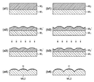
(第2実施形態)
図5を参照しながら第2実施形態を説明する。本実施形態は、主に、前述の第2の成形工程で、マイクロレンズの頂に部材M2’の一部mが残るようにエッチングを行う点で、前述の第1実施形態と異なる。部材M2’(M2)は透光性の材料で構成され、第1実施形態と同様にして、スチレン系樹脂が用いられうる。
(Second Embodiment)
The second embodiment will be described with reference to FIG. This embodiment is different from the first embodiment described above in that etching is performed so that a part m of the member M 2 ′ remains on the top of the microlens in the second molding step described above. The member M 2 ′ (M 2 ) is made of a translucent material, and a styrene resin can be used in the same manner as in the first embodiment.
図5は、本実施形態にかかるマイクロレンズML2の形成方法を工程ごとに説明するための模式図を、図2(第1実施形態)と同様にして示している。図5(a1)、(b1)、(a2)及び(b2)は、図2(a1)、(b1)、(a2)及び(b2)と同様であるため、ここでは説明を省略する。 FIG. 5 is a schematic diagram for explaining the method of forming the microlens ML2 according to the present embodiment for each step in the same manner as FIG. 2 (first embodiment). 5 (a1), (b1), (a2), and (b2) are the same as FIGS. 2 (a1), (b1), (a2), and (b2), and thus description thereof is omitted here.
その後、前述の第2の成形工程のエッチングを、マイクロレンズの頂に部材M2’の一部mが残るように行う。ここでは、エッチング時間を220秒としたことを除いて、第1実施形態と同様のエッチング条件を用いた。図5(a3)及び(b3)は、部材M2’のエッチング中の様子を示しており、その後、図5(a4)及び(b4)に示されるように、頂に部材M2’の一部mを有するマイクロレンズML2が形成される。 Thereafter, the etching in the second molding step is performed so that a part m of the member M 2 ′ remains on the top of the microlens. Here, the same etching conditions as in the first embodiment were used except that the etching time was 220 seconds. FIGS. 5 (a3) and (b3) show the state during the etching of the member M 2 ′, and then, as shown in FIGS. 5 (a4) and (b4), the top of the member M 2 ′ A microlens ML2 having a portion m is formed.
本実施形態によると、エッチング時間を短縮することができ、生産性の向上にも有利である。また、本実施形態によると、エッチング時間が短縮されるため、該エッチングによるパーティクルの発生を防ぐことができ、歩留まりの向上にも有利である。 According to this embodiment, the etching time can be shortened, which is advantageous in improving productivity. Further, according to the present embodiment, since the etching time is shortened, the generation of particles due to the etching can be prevented, which is advantageous in improving the yield.
マイクロレンズML2は、部材M1および部材M2’(M2)の2層の材料で構成される。そのため、固体撮像素子に適用する場合には、部材M1の屈折率と部材M2の屈折率との差を0.1以下にするとよく、これによって、該固体撮像素子から得られた画像の色むらが防止されうる。また、部材M2’の一部mは、マイクロレンズML2の頂(略水平な部分)のみに配されるため、この構造によるマイクロレンズML2の集光率に対する影響は小さい。 Microlens ML2 is constructed of a material of two layers of members M 1 and member M 2 '(M 2). Therefore, when applied to the solid-state imaging device may when the difference between the refractive index of the member M 1 and the refractive index of the member M 2 to 0.1 or less, thereby, the resulting image from the solid-state image capturing device Color unevenness can be prevented. In addition, since the part m of the member M 2 ′ is disposed only on the top (substantially horizontal portion) of the microlens ML2, the influence on the light collection rate of the microlens ML2 by this structure is small.
以上、本実施形態によると、第1実施形態と同様の効果が得られる他、生産性の向上および歩留まりの向上にも有利である。 As described above, according to the present embodiment, the same effects as those of the first embodiment can be obtained, and it is advantageous in improving productivity and yield.
(第3実施形態)
図6及び7を参照しながら第3実施形態を説明する。前述の第1実施形態では、部材M2’の凹凸形状を部材M1に転写する際に、部材M1と部材M2’とのエッチングレート差により、該部材M2’の凹凸形状の高低差よりも大きい高低差の凹凸形状を部材M1に形成することを述べた。このマイクロレンズの形状の制御は、さらに他の態様に応用することが可能である。例えば、第1の成形工程において、部材M2’を、その上面が対辺方向と対角方向とで曲率が互いに異なる凹凸形状になるように成形してもよい。
(Third embodiment)
A third embodiment will be described with reference to FIGS. In the first embodiment described above, 'the time of transferring the uneven shape of the member M 1, member M 1 and the member M 2' member M 2 by the etching rate difference between the high and low of the irregular shape of the member M 2 ' It said forming a concave-convex shape of the large difference in height than the difference in member M 1. The control of the shape of the microlens can be applied to other modes. For example, in the first forming step, the member M 2 ′ may be formed such that the upper surface thereof has an uneven shape with different curvatures in the opposite direction and the opposite direction.
図6は、本実施形態にかかるマイクロレンズML3の形成方法を工程ごとに説明するための模式図を、図2(第1実施形態)と同様にして示している。図6(a1)及び(b1)は、図2(a1)及び(b1)と同様であるため、ここでは説明を省略する。 FIG. 6 is a schematic diagram for explaining the method of forming the microlens ML3 according to the present embodiment for each step in the same manner as FIG. 2 (first embodiment). FIGS. 6A1 and 6B1 are the same as FIGS. 2A1 and 2B1, and thus description thereof is omitted here.
次に、図6(a2)及び(b2)に示されるように、第1の成形工程、即ち、部材M2を、その上面が凹凸形状になるように成形する工程を行う。この工程は、前述のとおり、グレースケールマスクを用いて部材M2を露光した後、現像することによってなされうる。ここで、本実施形態では、この工程で形成される部材M2’の凹凸形状が、対辺方向と対角方向とで互いに異なる曲率になるように、グレースケールマスクの露光光の透過率分布を調整している。 Next, as shown in FIG. 6 (a2) and (b2), the first molding step, i.e., a step of molding the member M 2, so that the upper surface is uneven. This process, as described above, after exposing the member M 2 using the gray scale mask may be made by developing. Here, in the present embodiment, the transmittance distribution of the exposure light of the grayscale mask is set so that the uneven shape of the member M 2 ′ formed in this step has different curvatures in the opposite direction and the opposite direction. It is adjusting.
図7は、本実施形態のグレースケールマスクの露光光の透過率分布を説明するための図である。図中において、縦軸Xは、透過率を示しており、横軸Yは、マイクロレンズアレイAMLの平面方向での位置(距離)を示している。なお、説明を容易にするため、露光処理に用いる露光装置の投影光学系の投影倍率を1倍とする。また、比較を容易にするため、ここでは、対辺方向と対角方向との透過率分布のそれぞれを、それらの中央で互いに重なるように示している。 FIG. 7 is a diagram for explaining the transmittance distribution of the exposure light of the grayscale mask of the present embodiment. In the figure, the vertical axis X indicates the transmittance, and the horizontal axis Y indicates the position (distance) in the plane direction of the microlens array AML . For ease of explanation, the projection magnification of the projection optical system of the exposure apparatus used for the exposure process is set to 1. Further, in order to facilitate comparison, here, the transmittance distributions in the opposite direction and the opposite direction are shown so as to overlap each other at the center thereof.
図7に示されるように、対辺方向の透過率分布の変化率は、対角方向の透過率分布の変化率よりも大きい。このグレースケールマスクを用いた露光処理および現像処理を行うことにより、部材M2の凹凸形状を、対辺方向の曲率が対角方向の曲率よりも大きくなるように形成することができる。
その後、前述と同様にして第2の成形工程がなされる。図6(a3)及び(b3)は、部材M2’のエッチング中の様子を示している。
As shown in FIG. 7, the change rate of the transmittance distribution in the opposite direction is larger than the change rate of the transmittance distribution in the diagonal direction. By performing the exposure processing and developing processing using the gray scale mask, a concavo-convex shape of the member M 2, the curvature of the opposite side direction can be formed to be larger than the curvature in the diagonal direction.
Thereafter, a second molding step is performed in the same manner as described above. FIGS. 6A3 and 6B3 show a state in which the member M 2 ′ is being etched.
第2の成形工程の後では、図6(a4)及び(b4)に示されるように、対辺方向での高低差と対角方向での高低差とがそれぞれ大きくなり、即ち、対辺方向での曲率と対角方向での曲率とがそれぞれ大きくなる。
本実施形態によると、第1実施形態と同様の効果が得られる他、マイクロレンズML3の形状を任意に制御することが可能であり、例えば、前述の一致率がより高く、又は、高低差もしくは曲率がより大きいマイクロレンズML3を形成するのにも有利である。
After the second molding step, as shown in FIGS. 6 (a4) and (b4), the height difference in the opposite direction and the difference in height in the opposite direction become larger, that is, in the opposite direction. The curvature and the curvature in the diagonal direction are increased.
According to the present embodiment, the same effects as those of the first embodiment can be obtained, and the shape of the microlens ML3 can be arbitrarily controlled. For example, the above-described matching rate is higher, or the height difference or It is also advantageous to form the microlens ML3 having a larger curvature.
以上、本実施形態では、マイクロレンズML3の形状を制御する態様を対辺方向および対角方向に着目して述べたが、本発明はこれに限られるものではない。例えば、本発明によると、図3に示された領域R1(上面が凸形状となる曲率を有する領域)を任意に制御することが可能である。即ち、第1の成形工程で形成される部材M2’の凹凸形状の制御と、第2の成形工程での部材M1と部材M2’とのエッチングレート比の選択とが可能であれば、マイクロレンズの形状を任意の形状に制御することが可能である。 As described above, in the present embodiment, the aspect of controlling the shape of the microlens ML3 has been described focusing on the opposite direction and the diagonal direction, but the present invention is not limited to this. For example, according to the present invention, it is possible to arbitrarily control the region R1 shown in FIG. 3 (region having a curvature with a convex upper surface). That is, if it is possible to control the uneven shape of the member M 2 ′ formed in the first molding step and to select the etching rate ratio between the member M 1 and the member M 2 ′ in the second molding step. The shape of the microlens can be controlled to an arbitrary shape.
例えば、マイクロレンズの集光率をさらに向上させるため、マイクロレンズを、領域R1の面積が領域R2の面積よりも大きくなるように形成するとよい。例えば、マイクロレンズアレイAMLに対する平面視において、領域R1の面積を領域R2の面積の4倍以上にするとよく、5倍以上にするとさらによい。 For example, in order to further improve the light collection rate of the microlens, the microlens may be formed so that the area of the region R1 is larger than the area of the region R2. For example, in a plan view with respect to the microlens array A ML , the area of the region R1 may be four times or more than the area of the region R2, and more preferably five times or more.
また、本実施形態においても、前述の第2実施形態と同様にして、マイクロレンズの頂に部材M2’の一部mが残るように、第2の成形工程のエッチングを行ってもよい。この方法によると、さらに、生産性の向上および歩留まりの向上にも有利である。 Also in this embodiment, similarly to the second embodiment described above, the etching in the second molding step may be performed so that a part m of the member M 2 ′ remains on the top of the microlens. This method is further advantageous for improving productivity and yield.
以上の各実施形態で形成されるマイクロレンズは、例えば、固体撮像素子に用いられうる。例えば、固体撮像素子の製造方法は、光電変換部が設けられた基板を準備する工程と、上記各実施形態のマイクロレンズの形成方法により、該基板の上に光電変換部に対応するマイクロレンズを形成する工程と、を有しうる。 The microlens formed in each of the above embodiments can be used for, for example, a solid-state imaging device. For example, in the method for manufacturing a solid-state imaging device, the microlens corresponding to the photoelectric conversion unit is formed on the substrate by the step of preparing the substrate provided with the photoelectric conversion unit and the microlens formation method of each of the above embodiments. Forming.
(第4実施形態)
本実施形態では、非対称マイクロレンズを備えた固体撮像素子を形成する工程を説明する。図8(b)に例示されるように、本実施形態に係る固体撮像素子は、レンズ中心に対して非対称な形状を持つ非対称マイクロレンズ804を備える。非対称マイクロレンズ804は、光電変換部、配線層およびカラーフィルターを有する構造809の上に設けられている。
(Fourth embodiment)
In the present embodiment, a process of forming a solid-state imaging device having an asymmetric microlens will be described. As illustrated in FIG. 8B, the solid-state imaging device according to the present embodiment includes an
非対称マイクロレンズ804は、固体撮像素子の撮像面周辺部に入射する斜め入射光を受光面に集光する。非対称マイクロレンズ804は、球面マイクロレンズと比較して、例えば、より入射角度が大きい入射光を集光できるようになるという点で有利である。球面マイクロレンズを用いる場合には、光電変換部で検出する斜め入射光の光量を増やすために、球面マイクロレンズを基板の面内方向にずらして配置することが行われる。しかし、このようなレンズずらし量が大きくなると、配線によって入射光が遮られることから、光電変換部への集光率が低くなる。一方、非対称マイクロレンズ804を用いると、レンズをずらす場合であっても、球面マイクロレンズを用いる場合と比べてレンズずらし量を小さくすることができ、集光率を向上させるのに有利である。また、非対称マイクロレンズ804を用いると、撮像面への光の入射角度を小さく抑えることができるため、混色を防ぐのにも有利である。
The
図8(b)に示されるように、非対称マイクロレンズ804を備える固体撮像素子において、領域808は、光電変換部への集光に寄与する領域であるため、領域808は、大きく設けられるとよい。一方、領域805は光電変換部への集光に寄与しない領域であり、かつ、領域805からの光は図8(b)に示されるように迷光成分となりうるため、領域805は、小さく設けられるとよい。
As shown in FIG. 8B, in the solid-state imaging device including the
図8(a1)から(a5)は、非対称マイクロレンズ804の形成方法を説明するための図である。図8(a1)は、非対称マイクロレンズ800の上面図である。図8(a2)は、カットラインA−A´の断面における非対称マイクロレンズ800の形状(設計上の形状)を示している。図8(a3)は、該非対称マイクロレンズ800の形状に対応するフォトマスクの光透過率の分布802を示している。図8(a4)は、フォトマスクを透過し、フォトレジストに照射される光の光強度分布803を示している。図8(a5)は、現像後のフォトレジストからなる非対称マイクロレンズ804の形状(現像後の形状)を示している。
FIGS. 8A1 to 8A5 are views for explaining a method of forming the
ここで、レンズ設計段階における非対称マイクロレンズの形状806は、露光・現像後における非対称マイクロレンズの形状807とは異なる形状となってしまう。すなわち、形状806は、急峻な形状として設計されているのに対して、プロセスの過程で、該急峻な形状は鈍った形状である形状807となる。図8(a3)及び(a4)に示すように、フォトマスクで光の透過率が急峻に変化する領域を設けたとしても、露光工程において発生する光の回折により、露光光の分布がなだらかになってしまい、鈍った形状となる。
Here, the asymmetric microlens shape 806 at the lens design stage is different from the asymmetric microlens shape 807 after exposure and development. That is, the
この光の回折によって鈍ってしまったレジストの形状を、急峻な形状にする工程を以下説明する。 The process of making the resist shape dull by the diffraction of light steep will be described below.
図9(a)は、平面視において各々の外形がティアドロップ型の複数の非対称マイクロレンズが配列されたマイクロレンズアレイ900を示している。図9(b1)は、第1の形成工程後のカットラインA−A’(対辺方向)の断面におけるマイクロレンズアレイ900の形状を示している。図9(b2)は、第1の形成工程後のカットラインB−B’(対角方向)の断面におけるマイクロレンズアレイ900の形状を示している。部材M1の上には、第1の形成工程の露光・現像によってパターニングされた部材M2´が形成されている。
FIG. 9A shows a
ここで、本実施形態では、図9(b1)及び(b2)に示されるように、第1の形成工程後において、対辺方向では部材M1の上面が露出していないが、対角方向では部材M1の上面が露出している例を示している。また、既に述べたように所望の形状を有するマイクロレンズを形成するためには、部材M1の上面の少なくとも一部が部材M2’で覆われていることが好ましい。 Here, in the present embodiment, as shown in FIGS. 9B1 and 9B2, after the first forming step, the upper surface of the member M1 is not exposed in the opposite direction, but the member in the diagonal direction. The example which the upper surface of M1 is exposed is shown. Further, in order to form a microlens having a desired shape, as already mentioned, it is preferable that at least a part of the upper surface of the member M1 is covered by a member M 2 '.
ところで、マイクロレンズが配置可能な面積を最大限に利用した理想的な曲率等を有する非対称マイクロレンズを設計する場合、対角方向のレンズの高さが、部材M2で形成可能な高さより高くなることがある。しかし、プロセス上、このような理想的な非対称マイクロレンズを形成することはできない。そこで、レンズの集光に寄与する領域が領域808であることから、相対的に集光に対する寄与が小さい対角方向の各マイクロレンズが隣接する領域については、M2’にレンズ形状が形成されない部分があることを許容したレンズ設計とすることがある。すなわち、対角方向の各マイクロレンズの隣接領域には曲率を有する部材が形成されておらず、平坦部となるような構成とする。これにより、プロセスの観点からも実現可能な構成が提供できる。このため、本実施形態では、図9(b2)に示されるように、対角方向については、部材M1の上面が覆われていない構成にしている。その一方で、対辺方向については、このような制約がないことから、図9(b1)に示されるように、部材M1の上面が露出していない構成にしている。
By the way, when designing an asymmetrical microlens having an ideal curvature and the like that makes maximum use of the area where the microlens can be arranged, the diagonal lens height is higher than the height that can be formed by the member M2. Sometimes. However, such an ideal asymmetric microlens cannot be formed in the process. Therefore, since the region that contributes to the condensing of the lens is the
以上の4つの実施形態を述べたが、本発明はこれらに限られるものではなく、目的、状態、用途及び機能その他の仕様に応じて、適宜、変更が可能であり、他の実施形態によってもなされうる。
なお、ここでは、カメラ等に代表される撮像システムに含まれる固体撮像素子に本発明を適用する態様を例示したが、撮像システムの概念には、撮影を主目的とする装置の他、撮影機能を補助的に備える装置(パーソナルコンピュータや携帯端末等)も含まれる。また、撮像システムは、固体撮像素子からの信号を処理する信号処理部をさらに含みうる。該信号処理部は、例えば、A/D変換器、該A/D変換器から出力されるデジタルデータを処理するプロセッサ等を含みうる。
Although the above-described four embodiments have been described, the present invention is not limited to these, and can be appropriately changed according to the purpose, state, application, function, and other specifications. Can be made.
In addition, although the aspect which applies this invention to the solid-state image sensor included in the imaging system represented by the camera etc. here was illustrated, in addition to the apparatus aiming at imaging | photography as the concept of an imaging system, imaging | photography function The apparatus (personal computer, a portable terminal, etc.) provided with auxiliary | assistant is included. The imaging system may further include a signal processing unit that processes a signal from the solid-state imaging device. The signal processing unit may include, for example, an A / D converter, a processor that processes digital data output from the A / D converter, and the like.
ML:マイクロレンズ、AML:マイクロレンズアレイ。 ML: Microlens, AML : Microlens array.
Claims (10)
第1の部材の上に、該第1の部材とは異なる材料からなる第2の部材を形成する第1工程と、
グレースケールマスクであるフォトマスクを用いて前記第2の部材を露光して現像することにより、前記第2の部材を、その上面が、複数の凸部と複数の凹部とを有する凹凸形状を有するように成形する第2工程と、
前記成形された前記第2の部材と前記第1の部材とをエッチングすることにより、少なくとも前記第1の部材から、前記複数の凸部に対応する前記複数のマイクロレンズを形成する第3工程と、を有し、
前記第2工程で形成された前記複数の凸部は、
第1の凸部と、
前記第1の凸部と対辺方向において隣り合う第2の凸部と、
前記第1の凸部と対角方向において隣り合う第3の凸部と、
を含み、
前記第2工程では、前記第1の部材の一部であって前記複数の凹部のうちの前記第1の凸部と前記第3の凸部との間の凹部の下に位置する一部が露出され、
前記第3工程では、前記第1の部材のエッチングレートが前記第2の部材のエッチングレートよりも大きい条件で、前記第2の部材のエッチングと前記第1の部材のエッチングとを行う
ことを特徴とするマイクロレンズアレイの形成方法。 A method of forming a microlens array in which a plurality of microlenses are formed in an array, and at least a part of the plurality of microlenses has an asymmetric shape,
Forming a second member made of a material different from that of the first member on the first member;
By developing by exposing the pre-Symbol second member by using a photomask which is a gray scale mask, the second member, the upper surface of its uneven shape having a plurality of projections and a plurality of recesses A second step of molding to have
A third step of forming the plurality of microlenses corresponding to the plurality of convex portions from at least the first member by etching the molded second member and the first member; Have
The plurality of convex portions formed in the second step are
A first convex portion;
A second protrusion adjacent to the first protrusion in the opposite direction;
A third convex portion diagonally adjacent to the first convex portion;
Including
In the second step, a part of the first member and a part of the plurality of concave portions located below the concave portion between the first convex portion and the third convex portion. Exposed,
Said in the third step, in greater condition than the etching rate of the first etching rate of member the second member, it intends rows and etching said etching of the second member first member A method for forming a microlens array .
ことを特徴とする請求項1に記載のマイクロレンズアレイの形成方法。 In the second step, other part of the first member that is located below the concave portion between the first convex portion and the second convex portion among the plurality of concave portions. 2. A method of forming a microlens array according to claim 1 , wherein a part of is not exposed .
ことを特徴とする請求項1または請求項2に記載のマイクロレンズアレイの形成方法。 The second member is made of a light-transmitting material, and in the third step, etching is performed so that a part of the second member remains on the top of each microlens. A method for forming a microlens array according to claim 1 or 2 .
ことを特徴とする請求項1から請求項3のいずれか1項に記載のマイクロレンズアレイの形成方法。 The microlens array according to any one of claims 1 to 3, wherein a difference between a refractive index of the first member and a refractive index of the second member is 0.1 or less. Forming method.
ことを特徴とする請求項1から請求項4のいずれか1項に記載のマイクロレンズアレイの形成方法。 The height difference of the microlens formed in the third step, claim from claim 1, wherein greater than the height difference of the irregularities of the said formed in the second step the second member 5. The method for forming a microlens array according to any one of 4 above.
前記第2の部材は、スチレン系樹脂で構成されている
ことを特徴とする請求項1から請求項5のいずれか1項に記載のマイクロレンズアレイの形成方法。 The first member is made of an acrylic resin,
The method for forming a microlens array according to any one of claims 1 to 5, wherein the second member is made of a styrene resin.
ことを特徴とする請求項1から請求項6のいずれか1項に記載のマイクロレンズアレイの形成方法。 In the third step, the claim 1 the difference between the etching rates of the first member etch rate and the second member, characterized in that the etching is performed within the range of 5 Å / sec 50 Å / sec The method for forming a microlens array according to claim 6 .
ことを特徴とする請求項1から請求項7のいずれか1項に記載のマイクロレンズアレイの形成方法。The method for forming a microlens array according to any one of claims 1 to 7, wherein the microlens array is formed.
前記複数のマイクロレンズの配列方向とは垂直な方向での断面において、前記第3工程における前記少なくとも一部は、前記第2工程における前記少なくとも一部に対応する凸部よりも急峻な形状を有するIn a cross section in a direction perpendicular to the arrangement direction of the plurality of microlenses, the at least part of the third step has a steeper shape than a convex portion corresponding to the at least part of the second step.
ことを特徴とする請求項8に記載のマイクロレンズアレイの形成方法。The method for forming a microlens array according to claim 8.
請求項1に記載のマイクロレンズアレイの形成方法により、前記基板の上に前記複数の光電変換部に対応する前記複数のマイクロレンズを形成する工程と、を有する
ことを特徴とする固体撮像素子の製造方法。
Preparing a substrate provided with a plurality of photoelectric conversion units;
The method of forming a microlens array of claim 1, the solid-state imaging device characterized by having the steps of forming a plurality of micro lenses corresponding to the plurality of photoelectric conversion units on the substrate Production method.
Priority Applications (3)
| Application Number | Priority Date | Filing Date | Title |
|---|---|---|---|
| JP2014234005A JP6012692B2 (en) | 2014-01-27 | 2014-11-18 | Method for forming microlens array and method for manufacturing solid-state imaging device |
| US14/591,467 US9349771B2 (en) | 2014-01-27 | 2015-01-07 | Microlens forming method and solid-state image sensor manufacturing method |
| CN201510031490.6A CN104808266B (en) | 2014-01-27 | 2015-01-22 | Method for forming micro lenses and solid state image sensor manufacture method |
Applications Claiming Priority (3)
| Application Number | Priority Date | Filing Date | Title |
|---|---|---|---|
| JP2014012765 | 2014-01-27 | ||
| JP2014012765 | 2014-01-27 | ||
| JP2014234005A JP6012692B2 (en) | 2014-01-27 | 2014-11-18 | Method for forming microlens array and method for manufacturing solid-state imaging device |
Publications (3)
| Publication Number | Publication Date |
|---|---|
| JP2015158663A JP2015158663A (en) | 2015-09-03 |
| JP2015158663A5 JP2015158663A5 (en) | 2016-02-12 |
| JP6012692B2 true JP6012692B2 (en) | 2016-10-25 |
Family
ID=53679784
Family Applications (1)
| Application Number | Title | Priority Date | Filing Date |
|---|---|---|---|
| JP2014234005A Active JP6012692B2 (en) | 2014-01-27 | 2014-11-18 | Method for forming microlens array and method for manufacturing solid-state imaging device |
Country Status (3)
| Country | Link |
|---|---|
| US (1) | US9349771B2 (en) |
| JP (1) | JP6012692B2 (en) |
| CN (1) | CN104808266B (en) |
Families Citing this family (7)
| Publication number | Priority date | Publication date | Assignee | Title |
|---|---|---|---|---|
| WO2016103430A1 (en) * | 2014-12-25 | 2016-06-30 | キヤノン株式会社 | Line sensor, image reading device, image formation device |
| JP2016149417A (en) | 2015-02-10 | 2016-08-18 | キヤノン株式会社 | Solid-state imaging device, manufacturing method thereof, and imaging system |
| TWI734716B (en) * | 2015-11-13 | 2021-08-01 | 日商凸版印刷股份有限公司 | Solid-state imaging element and its manufacturing method |
| JP6801230B2 (en) * | 2016-05-24 | 2020-12-16 | 凸版印刷株式会社 | Solid-state image sensor and electronic equipment |
| GB2553559B (en) * | 2016-09-08 | 2022-06-29 | Bae Systems Plc | Diffusers for head up displays |
| JP6911353B2 (en) * | 2016-12-28 | 2021-07-28 | 凸版印刷株式会社 | Manufacturing method of solid-state image sensor |
| CN114690282A (en) * | 2020-12-31 | 2022-07-01 | 中芯集成电路(宁波)有限公司 | Method for manufacturing lens |
Family Cites Families (13)
| Publication number | Priority date | Publication date | Assignee | Title |
|---|---|---|---|---|
| JP2001174607A (en) * | 1999-12-16 | 2001-06-29 | Ricoh Opt Ind Co Ltd | Method of forming curved face and optical device |
| JP2001201609A (en) * | 2000-01-19 | 2001-07-27 | Nippon Sheet Glass Co Ltd | Method for producing planer microlens and planar microlens produced by the method |
| JP2003172804A (en) | 2001-12-06 | 2003-06-20 | Matsushita Electric Ind Co Ltd | Microlens array and method for manufacturing the same |
| JP2004079932A (en) * | 2002-08-22 | 2004-03-11 | Sony Corp | Solid pickup element, and manufacturing method thereof |
| JP4450597B2 (en) * | 2003-09-24 | 2010-04-14 | 東京エレクトロン株式会社 | Method for forming a microlens |
| US7560295B2 (en) * | 2003-10-09 | 2009-07-14 | Aptina Imaging Corporation | Methods for creating gapless inner microlenses, arrays of microlenses, and imagers having same |
| JP4510613B2 (en) * | 2004-12-28 | 2010-07-28 | パナソニック株式会社 | Method for manufacturing solid-state imaging device |
| CN100444381C (en) | 2006-10-13 | 2008-12-17 | 中国科学院上海技术物理研究所 | Backward integrated micro-lens infrared focal plane detector and micro-lens producing method |
| JP4479834B2 (en) | 2008-01-24 | 2010-06-09 | ソニー株式会社 | Microlens manufacturing method and solid-state imaging device manufacturing method |
| JP5233404B2 (en) * | 2008-05-19 | 2013-07-10 | 凸版印刷株式会社 | Manufacturing method of density distribution mask and manufacturing method of microlens array |
| JP2011029277A (en) | 2009-07-22 | 2011-02-10 | Toshiba Corp | Method for manufacturing solid state imaging apparatus, and the solid state imaging apparatus |
| US8670171B2 (en) | 2010-10-18 | 2014-03-11 | Qualcomm Mems Technologies, Inc. | Display having an embedded microlens array |
| CN103890617B (en) * | 2011-11-29 | 2016-01-06 | 三菱丽阳株式会社 | The manufacture method of blooming, planar luminous body and blooming |
-
2014
- 2014-11-18 JP JP2014234005A patent/JP6012692B2/en active Active
-
2015
- 2015-01-07 US US14/591,467 patent/US9349771B2/en active Active
- 2015-01-22 CN CN201510031490.6A patent/CN104808266B/en active Active
Also Published As
| Publication number | Publication date |
|---|---|
| US20150214270A1 (en) | 2015-07-30 |
| US9349771B2 (en) | 2016-05-24 |
| CN104808266A (en) | 2015-07-29 |
| CN104808266B (en) | 2017-04-05 |
| JP2015158663A (en) | 2015-09-03 |
Similar Documents
| Publication | Publication Date | Title |
|---|---|---|
| JP6012692B2 (en) | Method for forming microlens array and method for manufacturing solid-state imaging device | |
| JP2008032912A (en) | Method of manufacturing microlens | |
| JP2007528515A (en) | Lens array and manufacturing method thereof | |
| JP5233404B2 (en) | Manufacturing method of density distribution mask and manufacturing method of microlens array | |
| JP6035744B2 (en) | Solid-state image sensor | |
| JP4629473B2 (en) | Manufacturing method of solid-state imaging device | |
| JP5239417B2 (en) | Microlens array manufacturing method, density distribution mask and design method thereof | |
| KR100698071B1 (en) | CMOS image sensor and method for manufacturing the same | |
| US11611056B2 (en) | Display apparatus and method for manufacturing the same | |
| JP2007193266A (en) | Method of manufacturing microlens array and microlens substrate | |
| JP5391701B2 (en) | Density distribution mask, design apparatus therefor, and manufacturing method of micro three-dimensional array | |
| TWI418026B (en) | Method for fabricating an image sensor device | |
| JP2006053558A (en) | Lens formation by pattern transfer of photoresist profile | |
| JP4249459B2 (en) | IMAGING DEVICE AND METHOD FOR FORMING BENDING UNIT IN IMAGING DEVICE | |
| JP6631004B2 (en) | Color solid-state imaging device and method of manufacturing the same | |
| JP5136288B2 (en) | Concentration distribution mask and manufacturing method thereof | |
| JP2002107942A (en) | Exposure method | |
| JP6311771B2 (en) | Solid-state image sensor | |
| JP5286821B2 (en) | Microlens array manufacturing method and density distribution mask | |
| JP5629964B2 (en) | Density distribution mask, manufacturing method thereof, and manufacturing method of microlens array | |
| JP2012109541A (en) | Manufacturing method of solid-state image pickup device | |
| WO2017030025A1 (en) | Color solid-state image capture element and method for manufacturing same | |
| JP4249586B2 (en) | Method for forming a microlens | |
| JP2010211078A (en) | Lens shape design method, imaging element, and photomask design method | |
| JP6536005B2 (en) | Method of manufacturing color filter and color filter |
Legal Events
| Date | Code | Title | Description |
|---|---|---|---|
| A521 | Request for written amendment filed |
Free format text: JAPANESE INTERMEDIATE CODE: A523 Effective date: 20151217 |
|
| A977 | Report on retrieval |
Free format text: JAPANESE INTERMEDIATE CODE: A971007 Effective date: 20151224 |
|
| A131 | Notification of reasons for refusal |
Free format text: JAPANESE INTERMEDIATE CODE: A131 Effective date: 20160107 |
|
| A521 | Request for written amendment filed |
Free format text: JAPANESE INTERMEDIATE CODE: A523 Effective date: 20160304 |
|
| TRDD | Decision of grant or rejection written | ||
| A01 | Written decision to grant a patent or to grant a registration (utility model) |
Free format text: JAPANESE INTERMEDIATE CODE: A01 Effective date: 20160822 |
|
| A61 | First payment of annual fees (during grant procedure) |
Free format text: JAPANESE INTERMEDIATE CODE: A61 Effective date: 20160920 |
|
| R151 | Written notification of patent or utility model registration |
Ref document number: 6012692 Country of ref document: JP Free format text: JAPANESE INTERMEDIATE CODE: R151 |