JP6009448B2 - Loop antenna - Google Patents
Loop antenna Download PDFInfo
- Publication number
- JP6009448B2 JP6009448B2 JP2013533279A JP2013533279A JP6009448B2 JP 6009448 B2 JP6009448 B2 JP 6009448B2 JP 2013533279 A JP2013533279 A JP 2013533279A JP 2013533279 A JP2013533279 A JP 2013533279A JP 6009448 B2 JP6009448 B2 JP 6009448B2
- Authority
- JP
- Japan
- Prior art keywords
- loop antenna
- dielectric substrate
- antenna according
- loop
- conductive
- Prior art date
- Legal status (The legal status is an assumption and is not a legal conclusion. Google has not performed a legal analysis and makes no representation as to the accuracy of the status listed.)
- Active
Links
- 239000000758 substrate Substances 0.000 claims description 114
- 230000003071 parasitic effect Effects 0.000 claims description 25
- 230000001939 inductive effect Effects 0.000 claims description 19
- 239000002131 composite material Substances 0.000 claims description 12
- 230000005540 biological transmission Effects 0.000 claims description 6
- 239000003990 capacitor Substances 0.000 claims description 5
- 230000005855 radiation Effects 0.000 claims description 4
- 230000005404 monopole Effects 0.000 description 13
- 230000008878 coupling Effects 0.000 description 11
- 238000010168 coupling process Methods 0.000 description 11
- 238000005859 coupling reaction Methods 0.000 description 11
- 239000000463 material Substances 0.000 description 6
- 238000013461 design Methods 0.000 description 5
- SXHLTVKPNQVZGL-UHFFFAOYSA-N 1,2-dichloro-3-(3-chlorophenyl)benzene Chemical compound ClC1=CC=CC(C=2C(=C(Cl)C=CC=2)Cl)=C1 SXHLTVKPNQVZGL-UHFFFAOYSA-N 0.000 description 4
- 230000005684 electric field Effects 0.000 description 4
- 230000006870 function Effects 0.000 description 4
- 238000000034 method Methods 0.000 description 4
- 230000008901 benefit Effects 0.000 description 3
- 230000009466 transformation Effects 0.000 description 3
- 238000004891 communication Methods 0.000 description 2
- 230000005284 excitation Effects 0.000 description 2
- 230000004048 modification Effects 0.000 description 2
- 238000012986 modification Methods 0.000 description 2
- 238000000926 separation method Methods 0.000 description 2
- 239000000654 additive Substances 0.000 description 1
- 230000002411 adverse Effects 0.000 description 1
- 238000013459 approach Methods 0.000 description 1
- 230000001413 cellular effect Effects 0.000 description 1
- 230000008859 change Effects 0.000 description 1
- 150000001875 compounds Chemical group 0.000 description 1
- 230000008094 contradictory effect Effects 0.000 description 1
- 238000010586 diagram Methods 0.000 description 1
- 230000000694 effects Effects 0.000 description 1
- 230000006872 improvement Effects 0.000 description 1
- 239000004615 ingredient Substances 0.000 description 1
- 238000003780 insertion Methods 0.000 description 1
- 230000037431 insertion Effects 0.000 description 1
- 238000007689 inspection Methods 0.000 description 1
- 230000007246 mechanism Effects 0.000 description 1
- 238000010295 mobile communication Methods 0.000 description 1
- 230000008569 process Effects 0.000 description 1
- 238000011160 research Methods 0.000 description 1
- 230000004044 response Effects 0.000 description 1
- 238000001228 spectrum Methods 0.000 description 1
- 239000000126 substance Chemical group 0.000 description 1
Images


Classifications
-
- H—ELECTRICITY
- H01—ELECTRIC ELEMENTS
- H01Q—ANTENNAS, i.e. RADIO AERIALS
- H01Q5/00—Arrangements for simultaneous operation of antennas on two or more different wavebands, e.g. dual-band or multi-band arrangements
- H01Q5/30—Arrangements for providing operation on different wavebands
- H01Q5/378—Combination of fed elements with parasitic elements
-
- H—ELECTRICITY
- H01—ELECTRIC ELEMENTS
- H01Q—ANTENNAS, i.e. RADIO AERIALS
- H01Q1/00—Details of, or arrangements associated with, antennas
- H01Q1/12—Supports; Mounting means
- H01Q1/22—Supports; Mounting means by structural association with other equipment or articles
- H01Q1/24—Supports; Mounting means by structural association with other equipment or articles with receiving set
- H01Q1/241—Supports; Mounting means by structural association with other equipment or articles with receiving set used in mobile communications, e.g. GSM
- H01Q1/242—Supports; Mounting means by structural association with other equipment or articles with receiving set used in mobile communications, e.g. GSM specially adapted for hand-held use
- H01Q1/243—Supports; Mounting means by structural association with other equipment or articles with receiving set used in mobile communications, e.g. GSM specially adapted for hand-held use with built-in antennas
-
- H—ELECTRICITY
- H01—ELECTRIC ELEMENTS
- H01Q—ANTENNAS, i.e. RADIO AERIALS
- H01Q1/00—Details of, or arrangements associated with, antennas
- H01Q1/36—Structural form of radiating elements, e.g. cone, spiral, umbrella; Particular materials used therewith
- H01Q1/38—Structural form of radiating elements, e.g. cone, spiral, umbrella; Particular materials used therewith formed by a conductive layer on an insulating support
-
- H—ELECTRICITY
- H01—ELECTRIC ELEMENTS
- H01Q—ANTENNAS, i.e. RADIO AERIALS
- H01Q1/00—Details of, or arrangements associated with, antennas
- H01Q1/48—Earthing means; Earth screens; Counterpoises
-
- H—ELECTRICITY
- H01—ELECTRIC ELEMENTS
- H01Q—ANTENNAS, i.e. RADIO AERIALS
- H01Q5/00—Arrangements for simultaneous operation of antennas on two or more different wavebands, e.g. dual-band or multi-band arrangements
-
- H—ELECTRICITY
- H01—ELECTRIC ELEMENTS
- H01Q—ANTENNAS, i.e. RADIO AERIALS
- H01Q5/00—Arrangements for simultaneous operation of antennas on two or more different wavebands, e.g. dual-band or multi-band arrangements
- H01Q5/30—Arrangements for providing operation on different wavebands
- H01Q5/307—Individual or coupled radiating elements, each element being fed in an unspecified way
- H01Q5/314—Individual or coupled radiating elements, each element being fed in an unspecified way using frequency dependent circuits or components, e.g. trap circuits or capacitors
- H01Q5/321—Individual or coupled radiating elements, each element being fed in an unspecified way using frequency dependent circuits or components, e.g. trap circuits or capacitors within a radiating element or between connected radiating elements
-
- H—ELECTRICITY
- H01—ELECTRIC ELEMENTS
- H01Q—ANTENNAS, i.e. RADIO AERIALS
- H01Q5/00—Arrangements for simultaneous operation of antennas on two or more different wavebands, e.g. dual-band or multi-band arrangements
- H01Q5/30—Arrangements for providing operation on different wavebands
- H01Q5/307—Individual or coupled radiating elements, each element being fed in an unspecified way
- H01Q5/342—Individual or coupled radiating elements, each element being fed in an unspecified way for different propagation modes
- H01Q5/357—Individual or coupled radiating elements, each element being fed in an unspecified way for different propagation modes using a single feed point
- H01Q5/364—Creating multiple current paths
-
- H—ELECTRICITY
- H01—ELECTRIC ELEMENTS
- H01Q—ANTENNAS, i.e. RADIO AERIALS
- H01Q5/00—Arrangements for simultaneous operation of antennas on two or more different wavebands, e.g. dual-band or multi-band arrangements
- H01Q5/30—Arrangements for providing operation on different wavebands
- H01Q5/378—Combination of fed elements with parasitic elements
- H01Q5/392—Combination of fed elements with parasitic elements the parasitic elements having dual-band or multi-band characteristics
-
- H—ELECTRICITY
- H01—ELECTRIC ELEMENTS
- H01Q—ANTENNAS, i.e. RADIO AERIALS
- H01Q7/00—Loop antennas with a substantially uniform current distribution around the loop and having a directional radiation pattern in a plane perpendicular to the plane of the loop
-
- H—ELECTRICITY
- H01—ELECTRIC ELEMENTS
- H01Q—ANTENNAS, i.e. RADIO AERIALS
- H01Q7/00—Loop antennas with a substantially uniform current distribution around the loop and having a directional radiation pattern in a plane perpendicular to the plane of the loop
- H01Q7/005—Loop antennas with a substantially uniform current distribution around the loop and having a directional radiation pattern in a plane perpendicular to the plane of the loop with variable reactance for tuning the antenna
-
- H—ELECTRICITY
- H01—ELECTRIC ELEMENTS
- H01Q—ANTENNAS, i.e. RADIO AERIALS
- H01Q9/00—Electrically-short antennas having dimensions not more than twice the operating wavelength and consisting of conductive active radiating elements
- H01Q9/04—Resonant antennas
- H01Q9/16—Resonant antennas with feed intermediate between the extremities of the antenna, e.g. centre-fed dipole
- H01Q9/26—Resonant antennas with feed intermediate between the extremities of the antenna, e.g. centre-fed dipole with folded element or elements, the folded parts being spaced apart a small fraction of operating wavelength
Landscapes
- Engineering & Computer Science (AREA)
- Computer Networks & Wireless Communication (AREA)
- Details Of Aerials (AREA)
- Support Of Aerials (AREA)
- Waveguide Aerials (AREA)
Description
本発明は移動ハンドセット及び他の応用形態のためのループアンテナに関し、詳細には、2つ以上の周波数帯において動作することができるループアンテナに関する。 The present invention relates to loop antennas for mobile handsets and other applications, and in particular to loop antennas that can operate in more than one frequency band.
最新の移動電話の工業デザインでは、薄型電話機の需要が増えていることから、アンテナのために残されたプリント回路基板(PCB)の面積はほとんどなく、多くの場合に、アンテナは非常に小さな外形にしなければならない。同時に、アンテナが動作することを期待される周波数帯の数も増えつつある。 Due to the increasing demand for thin phones in the latest mobile phone industrial design, there is little printed circuit board (PCB) space left for the antenna, and in many cases the antenna has a very small profile. Must be. At the same time, the number of frequency bands in which antennas are expected to operate is increasing.
単一の移動電話プラットフォームにおいて複数の無線プロトコルが用いられるとき、その第1の問題は、単一の広帯域アンテナが使用されるべきであるか、複数の狭帯域アンテナの方が相応しいかを判断することである。単一の広帯域アンテナを備える移動電話を設計することは、全ての必要な帯域をカバーするのに十分な帯域幅を得ることに関する問題だけでなく、信号を単向二路通信するために必要とされる回路の挿入損失、コスト、帯域幅及びサイズに関連付けられる難しさに関する問題も含む。一方、複数の狭帯域アンテナを用いる解決策は、アンテナ間の結合によって特徴付けられる問題、及びハンドセット上でアンテナのための十分な実装面積(real estate)を見つけることの難しさに関連付けられる。一般的に、これらの複数アンテナの問題は、広帯域の単一アンテナの問題よりも解決するのが難しい。 When multiple radio protocols are used in a single mobile phone platform, the first problem is to determine whether a single wideband antenna should be used or whether multiple narrowband antennas are more appropriate That is. Designing a mobile phone with a single broadband antenna is not only a matter of getting enough bandwidth to cover all the required bandwidth, but also necessary for one-way two-way communication of signals. It also includes issues related to the difficulty associated with the insertion loss, cost, bandwidth and size of the circuit being used. On the other hand, solutions using multiple narrowband antennas are associated with problems characterized by coupling between antennas and the difficulty of finding sufficient real estate for the antennas on the handset. In general, these multiple antenna problems are more difficult to solve than the broadband single antenna problem.
大部分の移動電話は一般的に、モノポールアンテナ又はPIFA(平面逆Fアンテナ)を使用する。モノポールは、PCB接地面又は他の導電面から離れているエリアにおい最も効率的に機能する。対照的に、PIFAは、導電面付近において良好に機能する。多大な研究努力がモノポールを形成することに注ぎ込まれており、PIFAは、複数のアンテナに関連付けられる問題を回避するように広帯域アンテナとして動作する。 Most mobile phones typically use a monopole antenna or PIFA (planar inverted F antenna). Monopoles function most efficiently in areas away from PCB ground planes or other conductive planes. In contrast, PIFA performs well near the conductive surface. A great deal of research effort has been put into forming monopoles, and the PIFA operates as a wideband antenna to avoid problems associated with multiple antennas.
電気的に小型のアンテナにおいて帯域幅を広げる1つの方法は、マルチモード化を利用することである。最も低い帯域では、奇数共振モードを引き起こすことができ、そのモードは「不平衡モード」、「差動モード」又は「モノポール相当」と様々に呼ばれる場合がある。より高い周波数では、偶数及び奇数両方の共振モードを引き起こすことができる。偶数モードは、「平衡モード」、「同相モード」又は「ダイポール相当」と様々に呼ばれる場合がある。 One way to increase bandwidth in an electrically small antenna is to use multi-mode. In the lowest band, an odd resonant mode can be caused, which may be variously called “unbalanced mode”, “differential mode” or “monopole equivalent”. Higher frequencies can cause both even and odd resonant modes. The even mode may be referred to variously as “balanced mode”, “common mode” or “dipole equivalent”.
ループアンテナは十分に理解されており、これまでに移動電話において使用されてきた。一例が特許文献1であり、高い帯域において放射する無給電接地モノポールとともに、低い帯域において放射する単一帯域接地ループを記述している。更なる例は特許文献2であり、ループを垂直に積重することによって小型化している対称ループアンテナ構造を開示している。アンテナのトップパッチにスタブを取り付けることによって、高い周波数帯域において広帯域特性が得られてきた。この構成が、無線通信の分野において有用なマルチモード化アンテナを生み出す。 Loop antennas are well understood and have been used in mobile phones so far. One example is US Pat. No. 6,057,056, which describes a single band ground loop radiating in the lower band along with a parasitic ground monopole radiating in the higher band. A further example is U.S. Pat. No. 6,057,086, which discloses a symmetrical loop antenna structure that is miniaturized by stacking loops vertically. By attaching a stub to the top patch of the antenna, broadband characteristics have been obtained in a high frequency band. This configuration creates a multimoded antenna that is useful in the field of wireless communications.
アンテナをマルチモード化する着想も新しくはない。ここで、良好な設計実践の一例が、モトローラ(登録商標)折り返し逆コンフォーマルアンテナ(Folded Inverted Conformal Antenna:FICA)であり、そのアンテナは、奇数共振モード及び偶数共振モードを示す構造において共振を励振する(非特許文献1)。高い帯域を得るために2つのモードが合成されるように記述されている。2つのモードとは、FICAアーム上の逆位相電流及びPCBグラウンド上の横方向電流を特徴とする「差動モード」、及びより高次の同相モードであり、FICAスロットの強い励振を特徴とする「スロットモード」である。それらのモードの組み合わせを用いて、広い連続した放射帯を生成することができる。しかしながら、参照されるFICA構造はPIFAの変形であり、非特許文献1の論文はループアンテナのマルチモード化を教示していない。
The idea of multi-mode antennas is not new. Here, an example of good design practice is the Motorola® Folded Inverted Conformal Antenna (FICA), which excites resonance in a structure that exhibits odd and even resonant modes. (Non-Patent Document 1). It is described that two modes are combined to obtain a high bandwidth. The two modes are “differential mode” characterized by antiphase current on the FICA arm and lateral current on the PCB ground, and higher order common mode, characterized by strong excitation of the FICA slot. “Slot mode”. A combination of these modes can be used to generate a wide continuous emission band. However, the referenced FICA structure is a modification of PIFA, and the paper of Non-Patent
本発明の実施の形態は、マルチモード化されたループアンテナ設計を使用する。本発明の実施の形態は、移動電話ハンドセットにおいて有用であり、移動モデムデバイス、例えば、ラップトップコンピュータが移動ネットワークを経由してインターネットと通信できるようにするためのUSBドングル等において用いることもできる。 Embodiments of the present invention use a multimode loop antenna design. Embodiments of the present invention are useful in mobile telephone handsets and can also be used in mobile modem devices, such as USB dongles for allowing laptop computers to communicate with the Internet via a mobile network.
本発明の第1の態様によれば、反対に位置する第1の表面及び第2の表面を有する誘電体基板と、該基板上に形成される導電性トラックとを備えるループアンテナであって、前記基板の前記第1の表面上に互いに隣接して給電点及び接地点が設けられ、前記導電性トラックは前記給電点及び前記接地点からそれぞれ反対の方向に延在し、次いで、前記誘電体基板のエッジに向かって延在し、次いで、前記誘電体基板の前記第2の表面に進み、次いで、前記誘電体基板の前記第1の表面上で辿った経路に従う経路に沿って前記誘電体基板の前記第2の表面にわたって進み、次いで、前記誘電体基板の前記第2の表面上に形成される導電性構成体のそれぞれの側に接続し、前記導電性構成体は、前記誘電体基板の前記第2の表面上に前記導電性トラックによって形成されたループの中央部の中に延在し、前記導電性構成体は誘導性素子及び容量性素子の両方を含む、ループアンテナが提供される。 According to a first aspect of the present invention, there is provided a loop antenna comprising a dielectric substrate having opposite first and second surfaces, and a conductive track formed on the substrate, A feeding point and a grounding point are provided adjacent to each other on the first surface of the substrate, and the conductive tracks extend in opposite directions from the feeding point and the grounding point, respectively, and then the dielectric The dielectric extends along an edge of the substrate, then proceeds to the second surface of the dielectric substrate, and then follows a path followed on the first surface of the dielectric substrate. Proceeding over the second surface of the substrate and then connecting to each side of a conductive structure formed on the second surface of the dielectric substrate, the conductive structure being connected to the dielectric substrate The conductive surface on the second surface of Tsu extends into the central portion of the loop formed by the click, the conductive structure comprises both inductive element and capacitive element, the loop antenna is provided.
その導電性構成体は、誘導性素子及び容量性素子の両方を含むという点で、電気的に複合的であると考えることができる。誘導性素子及び容量性素子は集中構成要素(例えば、個別の表面実装インダクタ及びコンデンサ)とすることもできるが、好ましい実施の形態では、それらの素子は分布構成要素、例えば、基板の第2の表面上又は表面内にある適切な形状を成す導電性トラックの領域として、形成又は印刷される。 The conductive structure can be considered electrically complex in that it includes both inductive and capacitive elements. Inductive and capacitive elements can be lumped components (eg, separate surface mount inductors and capacitors), but in a preferred embodiment they are distributed components, eg, a second of the substrate. Formed or printed as a region of conductive tracks of suitable shape on or in the surface.
特許文献2は、上面上にアンテナの高周波帯の帯域幅を広げるスタブを有する折り返しループアンテナを記述しているという点で、この構成は、特許文献2において開示される構成とは異なる。特許文献2は、「スタブは、周波数同調又は広帯域特性を得るために伝送ラインに更に接続されるラインである」と明記している。そのスタブは、「トップパッチに並列に接続されるシャントスタブであり、その長さがλ/4未満である開放スタブである」。また、特許文献2では、「長さ(スタブ)Lがλ/4未満であるときに、開放スタブがコンデンサとしての役割を果たす」ことも明記されている。本発明では、アンテナは、特許文献2において記述される簡単な容量性シャントスタブではなく、ループの中央において、又はその付近において直列の複合構造を含む。
This configuration differs from the configuration disclosed in
集中及び分布の両方の場合に、本発明の実施の形態の導電性構成体は、特許文献2において記述されるシャントスタブよりも小さく、アンテナ構造全体を、よりコンパクトにできるようにする。この構造の更なる利点は、低い帯域に如何なる悪影響も及ぼすことなく、高い帯域のインピーダンス帯域幅に同調できるようにすることである。これにより、高い帯域での整合を大きく改善できるようになる。 In both cases of concentration and distribution, the conductive structure of the embodiment of the present invention is smaller than the shunt stub described in US Pat. A further advantage of this structure is that it allows tuning to a high band impedance bandwidth without any adverse effect on the low band. Thereby, matching in a high band can be greatly improved.
誘導性素子及び容量性素子は、基板の第2の表面上に導電性トラックを形成して少なくとも1つのスロットを画定することによって、基板の第2の表面上のループの中央領域内に設けることができ、例えば、1つのトラックを、中央領域内に延在させ、その後他のトラックと概ね平行であるが、他のトラックと電気的に接触しないように延在させることによって設けることができる。 The inductive element and the capacitive element are provided in a central region of a loop on the second surface of the substrate by forming a conductive track on the second surface of the substrate to define at least one slot. For example, one track can be provided by extending into the central region and then extending generally parallel to the other track but not in electrical contact with the other track.
その導電性トラックは2つのアームを有するループを形成し、そのループは給電点において開始し、接地点において終端することは理解されよう。ループの2つのアームは、最初に、給電点及び接地点においてそれぞれ始まり、互いに離れるように延在し、次いで、誘電体基板のエッジに向かって延在する。好ましい実施の形態では、アームは、最初に給電点及び接地点から延在するときに同一直線上にあり、誘電体基板のエッジに向かって延在するときに概ね又は実質的に平行を成すが、他の構成(例えば、誘電体基板のエッジに向かって広がっていくか、又は近づいていく構成)も除外されない。 It will be appreciated that the conductive track forms a loop with two arms that starts at the feed point and ends at ground. The two arms of the loop first begin at the feed point and the ground point, respectively, extend away from each other, and then extend toward the edge of the dielectric substrate. In a preferred embodiment, the arms are collinear when initially extending from the feed and ground points, but generally or substantially parallel when extending toward the edge of the dielectric substrate. Other configurations (for example, configurations that expand toward or approach the edge of the dielectric substrate) are not excluded.
特に好ましい実施の形態では、ループのアームは誘電体基板のエッジに沿って、又はエッジ付近において互いに向かって延在する。アームは、互いに近づくように(例えば、給電点と接地点との間の距離と同程度に、又はその距離よりも近づくように)、又は互いに近づかないように延在することができる。他の実施の形態では、ループの一方のアームは基板のエッジに沿って又はエッジ付近に、延在することができるが、他方は基板のエッジに沿って又はエッジ付近に、延在しない。他の実施の形態では、アームは互いに向かって延在しないことが考えられる。 In a particularly preferred embodiment, the arms of the loop extend towards each other along or near the edge of the dielectric substrate. The arms can extend so that they are close to each other (eg, as close to or closer than the distance between the feed point and the ground point) or not close to each other. In other embodiments, one arm of the loop can extend along or near the edge of the substrate, while the other does not extend along or near the edge of the substrate. In other embodiments, it is contemplated that the arms do not extend toward each other.
誘電体基板の第1の表面上の導電性トラックは、誘電体基板を貫通して、ビア又は穴を経由して第2の表面に進む。代替的には、誘電体トラックは、誘電体基板のエッジを越えて、一方の表面から他方の表面に進むことができる。導電性トラックは、2つの場所において、基板の一方の側から基板の他方の側に進むことは理解されよう。これらの通路は、双方がビア又は穴を通ることができるか、双方が基板のエッジを越えることができるか、又は一方はビア若しくは穴を通り、他方はエッジを越えることができる。 Conductive tracks on the first surface of the dielectric substrate pass through the dielectric substrate and travel to the second surface via vias or holes. Alternatively, the dielectric track can travel from one surface to the other across the edge of the dielectric substrate. It will be appreciated that the conductive track travels from one side of the substrate to the other side of the substrate at two locations. These passages can both pass through vias or holes, both can cross the edge of the substrate, or one can pass through the via or hole and the other can cross the edge.
導電性トラック及び負荷プレートによって形成されるループは、誘電体基板の平面に対して垂直な鏡面において対称を成すことができ、給電点と接地点との間において基板のエッジまで進むことができる。さらに、導電性トラックは、負荷プレートがあるにもかかわらず、基板の第1の表面と第2の表面との間に画定される鏡面について概ね対称を成すことができる。しかしながら、他の実施の形態では、これらの平面において対称でない場合がある。非対称の実施の形態は、特に高い方の帯域において帯域幅を改善することができる不平衡ループを作製する際に役に立つことがある。しかしながら、この結果として、そのアンテナは、接地面の形状又はサイズに変化があるときの離調に対する耐性が低くなる。 The loop formed by the conductive track and the load plate can be symmetric in a mirror plane perpendicular to the plane of the dielectric substrate and can travel to the edge of the substrate between the feed point and the ground point. Further, the conductive track can be generally symmetric about a mirror surface defined between the first surface and the second surface of the substrate, despite the presence of the load plate. However, other embodiments may not be symmetric in these planes. Asymmetric embodiments may be useful in creating unbalanced loops that can improve bandwidth, especially in the higher band. However, as a result of this, the antenna is less resistant to detuning when there is a change in the shape or size of the ground plane.
都合の良いことに、導電性トラックには、その導電性トラックによって概ね画定されるループから延在する1つ又は複数の突起(spur)を設けることができる。1つ又は複数の突起はループの中に、又はループから外に、又は両方に延在することができる。これらの付加的な1つ又は複数の突起は放射モノポールとしての役割を果たし、スペクトル内の更なる共振に寄与し、それにより、アンテナの帯域幅を広げる。 Conveniently, the conductive track can be provided with one or more spurs extending from a loop generally defined by the conductive track. The one or more protrusions can extend into the loop, out of the loop, or both. These additional one or more protrusions serve as radiating monopoles and contribute to further resonances in the spectrum, thereby increasing the antenna bandwidth.
代替的に又は付加的に、少なくとも1つの無給電放射素子を設けることができる。これは、基板の第1の表面若しくは第2の表面上に、又は異なる基板(例えば、アンテナ及びその基板が実装されるマザーボード)上に形成することができる。無給電放射素子は接地される(接地面に接続される)場合があるか、又は接地されない場合がある導電性素子である。無給電放射素子を設けることによって、更なる無線プロトコル、例えば、ブルートゥース(登録商標)又はGPS(グローバルポジショニングシステム)動作のために用いることができる更なる共振を追加することができる。 Alternatively or additionally, at least one parasitic radiating element can be provided. This can be formed on the first surface or the second surface of the substrate, or on a different substrate (eg, the antenna and the motherboard on which the substrate is mounted). A parasitic radiating element is a conductive element that may or may not be grounded (connected to a ground plane). By providing a parasitic radiating element, additional resonances can be added that can be used for further wireless protocols, eg Bluetooth® or GPS (Global Positioning System) operation.
幾つかの実施の形態では、本発明のアンテナは、少なくとも4つ、好ましくは少なくとも5つの異なる周波数帯において動作することができる。 In some embodiments, the antenna of the present invention can operate in at least 4, preferably at least 5 different frequency bands.
本発明の第2の態様によれば、反対に位置する第1の表面及び第2の表面を有する誘電体基板と、該基板上に形成される導電性トラックとを備える無給電ループアンテナであって、前記基板の前記第1の表面上に互いに隣接して第1の接地点及び第2の接地点が設けられ、前記導電性トラックは前記第1の接地点及び前記第2の接地点からそれぞれ反対の方向に延在し、次いで、前記誘電体基板のエッジに向かって延在し、次いで、前記誘電体基板の前記第2の表面に進み、次いで、前記誘電体基板の前記第1の表面上で辿った経路に従う経路に沿って前記誘電体基板の前記第2の表面にわたって進み、次いで、前記誘電体基板の前記第2の表面上に形成される導電性負荷プレートにおいて接続し、前記導電性負荷プレートは前記誘電体基板の前記第2の表面上の前記導電性トラックによって形成されるループの中央部の中に延在し、前記無給電ループアンテナを励振するように構成される別の直接駆動されるアンテナを更に設けられる、無給電ループアンテナが提供される。 According to a second aspect of the present invention, there is provided a parasitic loop antenna including a dielectric substrate having first and second surfaces positioned opposite to each other, and a conductive track formed on the substrate. A first grounding point and a second grounding point are provided adjacent to each other on the first surface of the substrate, and the conductive track extends from the first grounding point and the second grounding point. Extending in opposite directions, then extending towards the edge of the dielectric substrate, then proceeding to the second surface of the dielectric substrate, and then the first of the dielectric substrate Proceeding over the second surface of the dielectric substrate along a path following a path followed on the surface, then connecting at a conductive load plate formed on the second surface of the dielectric substrate; The conductive load plate is the dielectric substrate. There is further provided another directly driven antenna extending into the center of the loop formed by the conductive track on the second surface and configured to excite the parasitic loop antenna. A parasitic loop antenna is provided.
前記別の駆動されるアンテナは、前記第1の接地点から延在する前記導電性トラックの部分に隣接して配置される、より小型のループアンテナの形をとることができ、第2のループアンテナは、給電点及び接地点を有し、誘導性結合によって前記無給電ループアンテナを駆動するように構成される。駆動アンテナは、無給電ループアンテナ及びその基板が取り付けられるマザーボード上に形成することできる。 The another driven antenna may take the form of a smaller loop antenna disposed adjacent to a portion of the conductive track extending from the first ground point, and a second loop. The antenna has a feeding point and a grounding point, and is configured to drive the parasitic loop antenna by inductive coupling. The driving antenna can be formed on a mother board to which a parasitic loop antenna and its substrate are attached.
代替的に、前記別の駆動されるアンテナは、誘導性結合によって前記無給電ループアンテナを駆動するように配置され、構成されるモノポールアンテナ、好ましくは短いモノポールの形をとることができる。モノポールは、無給電ループアンテナ及びその基板が取り付けられるマザーボードの裏面に形成することができる。 Alternatively, the further driven antenna can take the form of a monopole antenna, preferably a short monopole, arranged and configured to drive the parasitic loop antenna by inductive coupling. The monopole can be formed on the back surface of the mother board to which the parasitic loop antenna and its substrate are attached.
特許文献2は、垂直スタック構造によってコンパクトに形成された古典的な半ループアンテナを記述している。通常、半ループアンテナは、一端において給電され、他端において接地される導電性素子を備える。本発明の第2の態様は、両端において接地され、それゆえ、無給電である放射ループアンテナである。この無給電ループアンテナは、一般的に無給電ループアンテナよりも小さい別の被駆動アンテナによって励振される。被駆動アンテナ又は駆動アンテナは、WiFi周波数帯のうちの1つ等の、対象となる更に高い周波数において放射するように構成することができる。
負荷プレートは、その形状を一般的に長方形にすることができるか、又は他の形状を有することができ、例えば、三角形を成すことができる。負荷プレートは、さらに、負荷プレートの主部から延在するアーム若しくは突起又は他の延長部を設けられる場合がある。負荷プレートは、基板の第2の表面上に、全体として基板に対して平行な導電板として形成される。負荷プレートの一方のエッジは、第2の表面上において、第1の表面上の給電点と接地点との間に形成されるラインに従うことができる。負荷プレートの反対のエッジは、第2の表面上の導電性トラックによって形成されるループの概ね中心に位置することができる。 The load plate can be generally rectangular in shape or can have other shapes, for example, can be triangular. The load plate may further be provided with arms or protrusions or other extensions that extend from the main portion of the load plate. The load plate is formed on the second surface of the substrate as a conductive plate that is generally parallel to the substrate. One edge of the load plate can follow a line formed on the second surface between the feed point on the first surface and the ground point. The opposite edge of the load plate can be located approximately in the center of the loop formed by the conductive tracks on the second surface.
本発明の第3の態様によれば、反対に位置する第1の表面及び第2の表面を有する誘電体基板と、該基板上に形成される導電性トラックとを備える無給電ループアンテナであって、前記基板の前記第1の表面上に互いに隣接して第1の接地点及び第2の接地点が設けられ、前記導電性トラックは前記第1の接地点及び前記第2の接地点からそれぞれ反対の方向に延在し、次いで、前記誘電体基板のエッジに向かって延在し、次いで、前記誘電体基板の前記第2の表面に進み、次いで、前記誘電体基板の前記第1の表面上で辿った経路に従う経路に沿って前記誘電体基板の前記第2の表面にわたって進み、次いで、前記誘電体基板の前記第2の表面上に形成される導電性構成体のそれぞれの側において接続し、前記導電性構成体は、前記誘電体基板の前記第2の表面上の前記導電性トラックによって形成されるループの中央部の中に延在し、前記導電性構成体は誘導性素子及び容量性素子の両方を含み、前記無給電ループアンテナを励振するように構成される別の直接駆動されるアンテナが更に設けられる、無給電ループアンテナが提供される。 According to a third aspect of the present invention, there is provided a parasitic loop antenna including a dielectric substrate having first and second surfaces positioned opposite to each other, and a conductive track formed on the substrate. A first grounding point and a second grounding point are provided adjacent to each other on the first surface of the substrate, and the conductive track extends from the first grounding point and the second grounding point. Extending in opposite directions, then extending towards the edge of the dielectric substrate, then proceeding to the second surface of the dielectric substrate, and then the first of the dielectric substrate Proceed over the second surface of the dielectric substrate along a path that follows the path followed on the surface, and then on each side of the conductive structure formed on the second surface of the dielectric substrate The conductive structure is connected to the dielectric Extending into the center of the loop formed by the conductive track on the second surface of the plate, the conductive structure including both inductive and capacitive elements, the parasitic loop A parasitic loop antenna is provided, further provided with another directly driven antenna configured to excite the antenna.
本発明の第3の態様は、第2の態様の無給電励振機構と、第1の態様の電気的に複合的な導電性構成体とを組み合わせる。 The third aspect of the present invention combines the parasitic excitation mechanism of the second aspect and the electrically complex conductive structure of the first aspect.
第1の態様〜第3の態様のうちの任意のものと組み合わせることができる本発明の第4の態様では、前記ループアンテナは、直接接地される代わりに、少なくとも1つのインダクタ、少なくとも1つのコンデンサ、少なくとも1つの伝送ライン長、及びこれらの直列又は並列の任意の組み合わせを含むリストから選択される複合負荷を通して接地される。 In a fourth aspect of the invention that can be combined with any of the first to third aspects, the loop antenna is at least one inductor, at least one capacitor instead of being directly grounded. , Grounded through a composite load selected from a list including at least one transmission line length, and any combination of these in series or parallel.
さらに、前記ループアンテナの前記接地点は、前記アンテナが異なる周波数帯をカバーできるように、幾つかの異なる複合負荷間で切替可能である。 Furthermore, the ground point of the loop antenna can be switched between several different composite loads so that the antenna can cover different frequency bands.
既に説明された本発明の種々の実施の形態は、主PCBの接地面の空きエリア上にリフローで実装することができる表面実装(SMT)構成要素として、又は接地面の上方で機能する高架構造として構成することができる。 The various embodiments of the present invention that have already been described are elevated structures that function as surface mount (SMT) components that can be reflow mounted over open areas of the ground plane of the main PCB or that function above the ground plane. Can be configured.
高い電界強度の領域内の基板材料を除去することによって、損失を低減できることが更にわかった。例えば、電界が最も高いループアンテナの基板材料の中に中央切欠きを切り込むことができ、結果として、高い周波数帯において性能が改善される。 It has further been found that loss can be reduced by removing substrate material in regions of high electric field strength. For example, a central notch can be cut into the substrate material of the loop antenna with the highest electric field, resulting in improved performance at higher frequency bands.
複合的な中央負荷構造を有するアンテナの場合、中央ラインの両側に2つの切取り部を形成することが好都合であることがわかった。ここでもまた、効率上の利点は主に高い周波数帯において得られる。 In the case of an antenna having a complex central load structure, it has proved advantageous to form two cutouts on either side of the central line. Here again, the efficiency advantage is obtained mainly in the high frequency band.
そのループアンテナは、アンテナ基板の一部を貫通する切取り部のために中央エリアを空けておくように構成することができる。ここで、その目的は、損失を低減することではなく、むしろ、マイクロUSBコネクタ等を配置することができる容積を生み出すことである。アンテナをコネクタと同じ場所に、例えば、移動電話ハンドセットの底部に配置することが多くの場合に望ましい。 The loop antenna can be configured to leave a central area for a cutout that penetrates a portion of the antenna substrate. Here, the purpose is not to reduce the loss, but rather to create a volume in which a micro USB connector or the like can be placed. It is often desirable to place the antenna in the same location as the connector, for example, at the bottom of the mobile phone handset.
更なる実施の形態では、被駆動又は無給電アンテナに短い容量性スタブ又は誘導性スタブを取り付けて、帯域幅、インピーダンス整合及び/又は効率を改善できることがわかった。単一のシャント容量性スタブを用いる着想は、英国特許出願第0912368.8号及び特許文献2において以前に開示されているが、中央の複合負荷の一部として、幾つかのそのようなスタブを使用することが好都合であることがわかった。本出願人の同時係属の英国特許出願第0912368.8号において既に記述されているように、それらのスタブは、ループ構造の他の部分に接続されるときに都合良く用いることもできる。 In further embodiments, it has been found that a short capacitive or inductive stub can be attached to a driven or parasitic antenna to improve bandwidth, impedance matching and / or efficiency. The idea of using a single shunt capacitive stub has been previously disclosed in UK patent application No. 09123688.8 and US Pat. It has proven convenient to use. These stubs can also be conveniently used when connected to other parts of the loop structure, as already described in Applicant's co-pending UK patent application No. 0913688.8.
本発明の実施の形態は、主PCBの各側に1つのアンテナを配置して、すなわち、上面に1つアンテナ、及び下面上の上面アンテナの真下に1つのアンテナを配置して、88MHz〜108MHz帯に対して同調する電気的に小型のFMラジオアンテナと組み合わせて用いることができることがわかった。そのように近接して配置される2つのアンテナを使用することは、それらのアンテナ間の結合に起因して一般には問題であるが、本発明の実施の形態のループ設計、及びFMアンテナの性質(それ自体、1つのタイプのループ)によって、それらのアンテナ間を非常に良好に分離できることがわかった。 Embodiments of the present invention have one antenna on each side of the main PCB, ie, one antenna on the top surface and one antenna directly below the top antenna on the bottom surface, 88 MHz to 108 MHz. It has been found that it can be used in combination with an electrically small FM radio antenna that is tuned to the band. Using two antennas so close to each other is generally a problem due to the coupling between the antennas, but the loop design of the embodiment of the present invention and the nature of the FM antenna It has been found that (by itself, one type of loop) allows very good separation between the antennas.
電気的に小型のモノポール及びPIFAは高いリアクタンス性インピーダンスによって特徴付けられ、そのインピーダンスは、伝送ライン上の短い開放スタブが容量性であるのと同じようにして本質的に容量性である。大部分のループアンテナ構成は低いリアクタンス性インピーダンスを有し、そのインピーダンスは、伝送ライン上の短絡スタブが誘導性であるのと同じようにして本質的に誘導性である。これらのタイプのアンテナはいずれも50オーム無線システムに整合させる際に困難がある。モノポール及びPIFAと同様に、ループアンテナは、不平衡に、又はモノポール相当になるように、グラウンドに短絡させることができる。この場合、ループは半ループとしての役割を果たすことができ、接地面においてその影像(image)を「見る」ことができる。代替的には、ループアンテナは完全なループとすることができ、動作するために接地面を必要としない平衡モードを有する。 Electrically small monopoles and PIFAs are characterized by a high reactive impedance, which is essentially capacitive in the same way that a short open stub on the transmission line is capacitive. Most loop antenna configurations have a low reactance impedance, which is essentially inductive in the same way that a shorted stub on the transmission line is inductive. Both of these types of antennas have difficulty in matching to a 50 ohm radio system. Similar to monopoles and PIFAs, the loop antenna can be shorted to ground to be unbalanced or equivalent to a monopole. In this case, the loop can serve as a half-loop and can “see” its image on the ground plane. Alternatively, the loop antenna can be a complete loop and has a balanced mode that does not require a ground plane to operate.
本発明の実施の形態は、非常に広い帯域幅にわたって動作するように奇数モード及び偶数モードの両方において駆動される接地ループを含む。そのアンテナの動作が以下に更に詳細に説明されることになる。 Embodiments of the present invention include ground loops that are driven in both odd and even modes to operate over a very wide bandwidth. The operation of the antenna will be described in more detail below.
本発明の実施形態が、添付の図面を参照しながら以下に更に説明される。 Embodiments of the present invention are further described below with reference to the accompanying drawings.
図1は、特許文献2において開示されているループアンテに概ね類似の従来技術のループアンテナを概略図の形で示す。誘電体基板は、通常はFR4 PCB基板材料のスラブであるが、明確にするために図1には示されない。アンテナ1は導電性トラック2から形成されるループを含み、導電性トラックは、基板の第1の表面(この場合には下面)上にいずれも互いに隣接して配置される給電点3と接地点4との間に延在する。導電性トラック2は、給電点3及び接地点4かからそれぞれ概ね反対方向5、6に延在し、次いで、誘電体基板のエッジに向かって延在し(7、8)、次いで、誘電体基板のエッジに沿って進み(9、10)、次いで、誘電体基板の第2の表面に進む(11、12)。次いで、導電性トラック2は、誘電体基板の第1の表面上で辿った経路に概ね従う経路に沿って、誘電体基板の第2の表面にわたって進み、次いで、誘電体基板の第2の表面上に形成される導電性負荷プレート13において接続し、導電性負荷プレートは、誘電体基板の第2の表面上で導電性トラック2によって形成されるループ15の中央部14の中に延在する。
FIG. 1 shows, in schematic form, a prior art loop antenna that is generally similar to the loop antenna disclosed in US Pat. The dielectric substrate is usually a slab of FR4 PCB substrate material, but is not shown in FIG. 1 for clarity. The
FR4基板材料のスラブの上側層及び下側層を覆うように導電性トラック2が折り返されることを見てとることができる。給電点3及び接地点4は下面上にあり、接地面が全体としてアンテナ1と同じ対称軸を通して対称である場合には、入れ替えることができる。言い換えると、アンテナ1が対称である場合には、端点3、4のいずれかを給電点として使用し、他方を接地のために使用することができる。アンテナ1が全体として実装されることになるマザーボードが、その表面のうちの一方だけから点3及び4に給電することができるので、一般的には、給電点3及び接地点4はいずれもアンテナ基板の同じ表面上に存在することになる。しかしながら、給電トラックをいずれかの表面上に形成することができ、それでもそれぞれの給電点3又は接地点4に接続できるように、基板を貫通する穴又はビアを用いることができる。導電性負荷プレート13は、ループ15の電気的な中央部付近のアンテナの上面に配置される。
It can be seen that the
ループ15の最も大きな寸法が40mmであると考えると、導電性トラック2は全体として、その波長が約310mm〜360mmである移動通信低周波帯(824MHz〜960MHz)において約半波長であると理解することができる。この状況において、ループの入力インピーダンスは本質的に容量性であり、その結果、ループアンテナの場合に一般的であるよりも放射抵抗が高くなり、Qが小さくなる(帯域幅が広くなる)。したがって、そのアンテナは低周波帯において十分に機能し、必要とされる帯域幅にわたって整合させるのは、それほど難しいことではない。アンテナ1は折り重ねられたループとして形成されるので、或る特定の実施形態では、その自己容量が動作周波数を低減するのを助ける。
Considering that the largest dimension of the
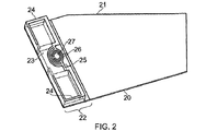
図2は、図1の従来技術のアンテナより優れた改善形態を示す。導電性接地面21を含むPCB基板20が示される。PCB基板20はエッジ部分22を有し、エッジ部分22は、本発明の一実施形態のアンテナ構造22を実装するための接地面21の空き部分である。アンテナ構造22は、反対に位置する第1の表面及び第2の表面を有する誘電体基板23(例えば、FR4又はDuroid(登録商標)等)を含む。導電性トラック24が基板23上に(例えば、印刷によって)形成され、図1に示される全体構成に類似の全体構成、すなわち、垂直方向にコンパクトに配置されたループからなる全体構成を有し、給電点26及び接地点25が基板の第1の表面上で互いに隣接し、導電性トラック24は、給電点26及び接地点25からそれぞれ概ね反対方向に延在し、次いで、誘電体基板23のエッジに向かって進み、次いで、誘電体基板23の第2の表面に進み、次いで、誘電体基板23の第1の表面上で辿った経路に概ね従う経路に沿って、誘電体基板23の第2の表面にわたって進む。次いで、基板23の第2の表面上の導電性トラック24の2つの端部は誘電体基板23の第2の表面上に形成される導電性構成体27のそれぞれの側に接続し、導電性構成体27は、誘電体基板23の第2の表面上に導電性トラック24によって形成されるループの中央部の中に延在し、導電性構成体27は、誘導性素子及び容量性素子の両方を含む。図1の構成と比べると、高周波帯の整合が大きく改善される。
FIG. 2 shows an improvement over the prior art antenna of FIG. A
図3は、図2の構成の変形形態を示しており、類似の部分は図2の場合と同じ番号を付される。この実施形態は、スタブ28及びスロット29、30によって、基板23の第2の表面の中央部において電気的に複合的な(すなわち、誘導性及び容量性の)負荷を与える。この技法も、ループの中央付近においてインダクタンス及びキャパシタンスを追加する。
FIG. 3 shows a variation of the configuration of FIG. 2, and similar parts are given the same numbers as in FIG. This embodiment provides an electrically complex (ie, inductive and capacitive) load at the center of the second surface of the
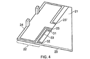
図4は、導電性トラック24によって画定される主ループアンテナが両方の端子25、25’においてグラウンド21に接続される変形形態を示す(明確にするために、今度は、図面から基板23及びアンテナの上半分を省略する)。言い換えると、主ループアンテナは、図2及び図3の場合のように、給電点26によって直接駆動されない。代わりに、主ループアンテナは、接地面21が存在しないPCB基板20の端部22上に形成される、より小型の別の被駆動ループアンテナ33によって励振され、被駆動ループアンテナ33は給電点31及び接地点32の接続を有する。より小型の被駆動ループアンテナ33は、WiFi周波数帯のうちの1つ等の、対象となる、より高い周波数において放射するように構成することができる。
FIG. 4 shows a variant in which the main loop antenna defined by the
この誘導性結合給電構成は、最適なインピーダンス整合を得るために変更することができる数多くのパラメータを有する。整合前後のアンテナの性能の一例が、図5に示される。全体としてアンテナのインピーダンス応答を調整するために、小さな結合ループ23のグラウンド32に、集中又は同調可能L素子及びC素子を追加することができる。
This inductively coupled feed configuration has a number of parameters that can be changed to obtain optimal impedance matching. An example of the antenna performance before and after matching is shown in FIG. Lumped or tunable L and C elements can be added to the
無給電ループアンテナ33の誘導性給電の変形形態では、無給電主ループは、主PCB20の上面にあるアンテナ部分に、主PCB基板20の下側にある短いモノポールを結合することによって、容量性結合を通して給電することができる。この構成は、本出願に対して先行する特許出願、英国特許出願第0914280.3号において開示された。
In a variant of inductive feeding of the
主ループアンテナを直接接地する代わりに、インダクタ、コンデンサ若しくは伝送ラインの長さ、又はこれらの直列及び並列の任意の組み合わせを含む複合負荷を通してアンテナを接地することが好都合である場合もある。さらに、アンテナが種々の周波数帯をカバーできるようにするために、図6に示されるように、幾つかの異なる複合負荷間でアンテナの接地点を切り替えることができる。図6は、主PCB基板20の接地接続25及び接地面21を示す。接地接続25は、スイッチ34によって接地面21に接続し、スイッチ34は、種々の誘導性構成要素及び/又は容量性構成要素35又は36に切り替えることができるか、又は直接接続37を与えることができる。以下に示される例では、スイッチ位置1では、アンテナの低周波帯がLTE帯700MHz〜760MHzをカバーし、スイッチ位置2では、750MHz〜800MHzをカバーし、スイッチ位置3では、GSM帯824MHz〜960MHzをカバーするように、複合接地負荷を選択した。
Instead of directly grounding the main loop antenna, it may be advantageous to ground the antenna through a composite load that includes the length of the inductor, capacitor or transmission line, or any combination of these in series and parallel. Further, to allow the antenna to cover various frequency bands, the antenna ground point can be switched between several different composite loads, as shown in FIG. FIG. 6 shows the
強い電界強度の領域内の基板23材料を除去することによって、損失を低減することができることがわかった。図7に示される例では、電界が最も高い基板材料23の中に中央切欠き38が切り込まれ、結果として、高周波帯において性能が改善された。
It has been found that the loss can be reduced by removing the
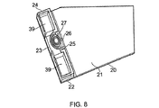
図8は、図2の実施形態の変形形態を示しており、基板23の一部が、中央複合負荷27の両側において第2の表面から切り取られる。この例では、切取り部は、形状が概ね立方体状であるが、他の形状及び容積も役に立つ場合がある。効率に関する利点は主に高い周波数帯において得られる。
FIG. 8 shows a variation of the embodiment of FIG. 2 in which a portion of the
図9及び図10は、主ループアンテナが基板23上のトラック24及び複合負荷27によって画定され、アンテナ基板23の一部を垂直に貫通する切取り部40のために中央領域42を空けておくように構成される変形形態を示す。ここで、その目的は、損失を低減することではなく、むしろ、マイクロUSBコネクタ41等を配置することができる容積を生み出すことである。アンテナをコネクタと同じ場所に、例えば、移動電話ハンドセットの底部に配置することが多くの場合に望ましい。
9 and 10 show that the main loop antenna is defined by a
更なる実施形態では、図11に示されるように、被駆動又は無給電ループアンテナ24に短い容量性スタブ又は誘導性スタブ43を取り付けて、帯域幅、インピーダンス整合及び/又は効率を改善できることがわかった。中央複合負荷27の一部として、幾つかのそのようなスタブ43を用いることが特に好都合であることがわかった。また、スタブ43は、ループ構造24の他の部分に接続されるときに都合良く用いることもできる。効率を改善するために、基板23内に切取り部39を設けることもできる。
In a further embodiment, it can be seen that a short capacitive or
図12は、88MHz〜108MHz帯域に同調し、主PCB20の、ループアンテナ24が実装される面と反対の面に実装される電気的に小型のFMラジオアンテナ44と組み合わせた、図9及び図10の実施形態に概ね対応する本発明の一実施形態を示す。言い換えると、一方のアンテナはPCB20の上面上にあり、他方のアンテナは、一方のアンテナの真下の主PCB20の下面上にある。そのように近接して配置される2つのアンテナを使用することは、それらのアンテナ間の結合に起因して一般には問題であるが、本発明の実施形態のループ設計、及びFMアンテナの性質(それ自体、1つのタイプのループ)によって、それらのアンテナ間を非常に良好に分離できることがわかった。
12 is combined with an electrically small
図13は、2つのアンテナ24と44(下側プロット)との間の結合が、セルラ帯の全体にわたって−30dB未満であることを示す。
FIG. 13 shows that the coupling between the two
本明細書の説明及び特許請求の範囲全体を通じて、語句「含む(comprise)」及び「含有する(contain)」及びそれらの変形は、「含むがこれらに限定されない(including but not limited to)」ことを意味し、それらは、他の部分、添加剤、成分、整数又は工程を除外するように意図されるものでない(またこれらを除外するものでもない)。本明細書中の説明及び特許請求の範囲全体を通じて、文脈上異なる解釈を要する場合を除き、数量が特定されていない場合、単数及び複数を含む(the singular encompasses the plural)。とりわけ、不定冠詞を使用する場合、本明細書は、文脈上異なる解釈を要する場合を除き、単数と同様に複数についても考えるものと解されるべきである。 Throughout the description and claims, the terms “comprise” and “contain” and variations thereof are “including but not limited to”. And they are not intended to exclude (or exclude) other parts, additives, ingredients, integers or steps. Throughout the description and claims throughout this specification, the singular and the plural are included unless a quantity is specified, unless the context requires otherwise. In particular, when using indefinite articles, the specification should be construed to consider the plural as well as the singular unless the context requires a different interpretation.
本発明の特定の態様、実施形態又は例と併せて記載される、特徴、整数、特性、化合物、化学的部分又は群は、矛盾しない限り、本明細書中に記載される他の任意の態様、実施形態又は例にも適用できると解されるべきである。本明細書(任意の添付の特許請求の範囲、要約書及び図面を含む)に開示される特徴の全て、及び/又はそのように開示される任意の方法及びプロセスの工程の全ては、かかる特徴及び/又は工程の少なくとも幾つかが互いに排他的である組合せを除き、任意の組合せで組み合わせることができる。本発明は、上述のいずれかの実施形態の詳細に限定されるものではない。本発明は、本明細書(任意の添付の特許請求の範囲、要約書及び図面を含む)に開示される特徴の、任意の新規な特徴若しくは任意の新規な組合せに、又はそのように開示される任意の方法若しくはプロセスの工程の、任意の新規な工程、若しくは任意の新規な組合せにも及ぶ。 Features, integers, properties, compounds, chemical moieties or groups described in conjunction with a particular aspect, embodiment or example of the invention, are not limited to any other aspect described herein unless otherwise contradictory. It should be understood that the present invention can also be applied to the embodiments or examples. All of the features disclosed in this specification (including any appended claims, abstract and drawings) and / or all of the steps of any methods and processes so disclosed are such features. And / or can be combined in any combination except combinations where at least some of the steps are mutually exclusive. The present invention is not limited to the details of any of the above-described embodiments. The present invention is disclosed in any novel feature or any novel combination of features disclosed herein (including any appended claims, abstract and drawings), or as such. It extends to any new step or any new combination of steps of any method or process.
読み手の注意は、本出願に関連して、本明細書と同時に又は本明細書に先立って提出され、かつ本明細書とともに公衆の閲覧に付される、全ての論文及び書類に向けられるものであり、全てのこのような論文及び書類の中身は、引用することにより本明細書中の一部をなすものとする。 Reader's attention is directed to all papers and documents that are filed with or prior to this specification and subject to public inspection in conjunction with this application. Yes, the contents of all such papers and documents are hereby incorporated by reference.
Claims (23)
前記誘電体基板の前記第1の表面において互いに隣接する給電点及び接地点が設けられ、
前記導電性トラックは、前記給電点及び前記接地点からそれぞれ反対の方向に延在し、前記誘電体基板のエッジに沿って延在し、前記誘電体基板の前記第2の表面に至り、前記誘電体基板の前記第1の表面上で辿った経路に従う経路に沿って前記誘電体基板の前記第2の表面上に延在し、前記誘電体基板の前記第2の表面上に形成される導電性構成体の両側に接続し、
前記導電性構成体は、(i)複数の同心円の一部に沿って互いに平行に延在する複数の導電性経路部分を形成するように、前記誘電体基板の前記第2の表面上における前記導電性トラックによって形成されるループの中央部に延在し、及び、(ii)スタブ及びスロットのうち少なくとも一方により形成される誘導性素子及び容量性素子の両方を含む、ループアンテナ。 A loop antenna having a dielectric substrate having a first surface and an opposite second surface, and a conductive track formed on the dielectric substrate,
A feeding point and a grounding point adjacent to each other are provided on the first surface of the dielectric substrate;
The conductive tracks extend in opposite directions from the feeding point and the grounding point, extend along an edge of the dielectric substrate, reach the second surface of the dielectric substrate, and Extending on the second surface of the dielectric substrate along a path following a path followed on the first surface of the dielectric substrate and formed on the second surface of the dielectric substrate Connected to both sides of the conductive structure,
The conductive structure comprises: (i) the conductive substrate on the second surface of the dielectric substrate so as to form a plurality of conductive path portions extending parallel to each other along a part of the plurality of concentric circles. A loop antenna that extends to the center of the loop formed by the conductive track and includes (ii) both inductive and capacitive elements formed by at least one of stubs and slots.
Applications Claiming Priority (3)
| Application Number | Priority Date | Filing Date | Title |
|---|---|---|---|
| GB1017472.0A GB2484540B (en) | 2010-10-15 | 2010-10-15 | A loop antenna for mobile handset and other applications |
| GB1017472.0 | 2010-10-15 | ||
| PCT/GB2011/051837 WO2012049473A2 (en) | 2010-10-15 | 2011-09-28 | A loop antenna for mobile handset and other applications |
Publications (3)
| Publication Number | Publication Date |
|---|---|
| JP2013545357A JP2013545357A (en) | 2013-12-19 |
| JP2013545357A5 JP2013545357A5 (en) | 2014-11-06 |
| JP6009448B2 true JP6009448B2 (en) | 2016-10-19 |
Family
ID=43333909
Family Applications (1)
| Application Number | Title | Priority Date | Filing Date |
|---|---|---|---|
| JP2013533279A Active JP6009448B2 (en) | 2010-10-15 | 2011-09-28 | Loop antenna |
Country Status (13)
| Country | Link |
|---|---|
| US (3) | US9502771B2 (en) |
| EP (2) | EP2628209B1 (en) |
| JP (1) | JP6009448B2 (en) |
| KR (1) | KR101837225B1 (en) |
| CN (1) | CN103155281B (en) |
| BR (1) | BR112013008761A2 (en) |
| CA (1) | CA2813829C (en) |
| GB (2) | GB2500136B (en) |
| IN (1) | IN2013MN00694A (en) |
| RU (1) | RU2586272C2 (en) |
| SG (1) | SG189210A1 (en) |
| TW (2) | TWI549373B (en) |
| WO (1) | WO2012049473A2 (en) |
Families Citing this family (43)
| Publication number | Priority date | Publication date | Assignee | Title |
|---|---|---|---|---|
| GB2500136B (en) | 2010-10-15 | 2015-02-18 | Microsoft Corp | Parasitic folded loop antenna |
| GB2484542B (en) | 2010-10-15 | 2015-04-29 | Microsoft Technology Licensing Llc | LTE antenna pair for mimo/diversity operation in the LTE/GSM bands |
| US10116062B2 (en) * | 2012-05-07 | 2018-10-30 | Sony Mobile Communications Inc. | Looped multi-branch planar antennas having a floating parasitic element and wireless communications devices incorporating the same |
| EP2733787B1 (en) * | 2012-06-28 | 2017-09-06 | Murata Manufacturing Co., Ltd. | Antenna device and communication terminal device |
| TWI495192B (en) * | 2012-07-27 | 2015-08-01 | Askey Computer Corp | Multiband antenna |
| TWI513105B (en) | 2012-08-30 | 2015-12-11 | Ind Tech Res Inst | Dual frequency coupling feed antenna, cross-polarization antenna and adjustable wave beam module |
| US9425496B2 (en) | 2012-09-27 | 2016-08-23 | Apple Inc. | Distributed loop speaker enclosure antenna |
| US8922443B2 (en) | 2012-09-27 | 2014-12-30 | Apple Inc. | Distributed loop antenna with multiple subloops |
| JP5839236B2 (en) * | 2012-10-16 | 2016-01-06 | カシオ計算機株式会社 | Mobile device |
| DE102012221940B4 (en) * | 2012-11-30 | 2022-05-12 | Robert Bosch Gmbh | Wireless communication module and method of making a wireless communication module |
| TWI619304B (en) * | 2013-05-17 | 2018-03-21 | 群邁通訊股份有限公司 | Broadband antenna and wireless communication device using same |
| WO2014188747A1 (en) * | 2013-05-20 | 2014-11-27 | 株式会社村田製作所 | Antenna and wireless communication device |
| CN104253300A (en) * | 2013-06-26 | 2014-12-31 | 重庆美桀电子科技有限公司 | Dual-band antenna capable of transmitting and receiving WiFi (Wireless Fidelity) and GPS (Global Positioning System) signals |
| US9350077B1 (en) * | 2013-08-08 | 2016-05-24 | Amazon Technologies, Inc. | Low SAR folded loop-shaped antenna |
| JP6131816B2 (en) | 2013-10-07 | 2017-05-24 | 株式会社デンソー | Modified folded dipole antenna |
| CN104577304B (en) * | 2013-10-18 | 2019-07-23 | 深圳富泰宏精密工业有限公司 | Antenna structure and wireless communication device with the antenna structure |
| CN104752819B (en) * | 2013-12-31 | 2019-11-01 | 深圳富泰宏精密工业有限公司 | Antenna structure and wireless communication device with the antenna structure |
| WO2015100654A1 (en) * | 2013-12-31 | 2015-07-09 | 华为终端有限公司 | Loop antenna and mobile terminal |
| US20150303551A1 (en) * | 2014-04-16 | 2015-10-22 | King Slide Technology Co.,Ltd. | Communication device antenna |
| US9184494B1 (en) * | 2014-05-09 | 2015-11-10 | Futurewei Technologies, Inc. | Switchable Pi shape antenna |
| KR20160067541A (en) * | 2014-12-04 | 2016-06-14 | 엘지전자 주식회사 | Antenna module and mobile terminal using the same |
| DE212016000166U1 (en) * | 2015-06-30 | 2018-03-13 | Murata Manufacturing Co., Ltd. | Coupling support device and RFID communication system |
| KR20170055351A (en) | 2015-11-11 | 2017-05-19 | 삼성전자주식회사 | Antenna device and electronic device including the same |
| GB2545918B (en) * | 2015-12-30 | 2020-01-22 | Antenova Ltd | Reconfigurable antenna |
| CN205376750U (en) * | 2016-01-12 | 2016-07-06 | 中磊电子(苏州)有限公司 | Dual -band antenna |
| KR20170103315A (en) * | 2016-03-03 | 2017-09-13 | 엘지전자 주식회사 | Mobile terminal |
| US20170374684A1 (en) * | 2016-06-24 | 2017-12-28 | Chittabrata Ghosh | Identifier assignment for unassociated stations |
| CN107645038B (en) * | 2016-07-20 | 2019-11-29 | 华为技术有限公司 | A kind of antenna and mobile terminal |
| US10103435B2 (en) * | 2016-11-09 | 2018-10-16 | Dell Products L.P. | Systems and methods for transloop impedance matching of an antenna |
| US10320078B2 (en) * | 2016-11-18 | 2019-06-11 | QuantalRF AG | Small form factor CPL antenna with balanced fed dipole electric field radiator |
| CN108288750B (en) * | 2017-01-10 | 2021-10-22 | 摩托罗拉移动有限责任公司 | Antenna system having feed line conductors at least partially spanning gaps between open ends of arms |
| US10165574B2 (en) * | 2017-01-31 | 2018-12-25 | Qualcomm Incorporated | Vehicle-to-everything control channel design |
| WO2019003683A1 (en) * | 2017-06-27 | 2019-01-03 | 株式会社村田製作所 | Dual band compatible antenna device |
| EP3422473B1 (en) | 2017-06-30 | 2021-07-28 | GN Audio A/S | Antenna structure for a headset |
| KR102469571B1 (en) * | 2018-01-25 | 2022-11-22 | 삼성전자주식회사 | Electronic device including loop type antenna |
| ES2737879A1 (en) * | 2018-07-16 | 2020-01-16 | Verisure Sarl | Printed circuit board for the control unit of an alarm system (Machine-translation by Google Translate, not legally binding) |
| KR102241220B1 (en) * | 2019-09-20 | 2021-04-19 | (주)파트론 | Antenna structure |
| KR102251239B1 (en) * | 2019-09-20 | 2021-05-13 | (주)파트론 | Antenna structure |
| TWI700862B (en) * | 2019-10-23 | 2020-08-01 | 華碩電腦股份有限公司 | Loop-like dual-antenna system |
| CN113725611B (en) * | 2019-10-31 | 2023-07-28 | 华为终端有限公司 | Antenna device and electronic equipment |
| CN110970706B (en) * | 2019-11-20 | 2021-04-09 | 珠海格力电器股份有限公司 | Multimode antenna, terminal, communication method and device of multimode antenna and processor |
| CN111276810A (en) * | 2020-02-18 | 2020-06-12 | 环鸿电子(昆山)有限公司 | Chip antenna |
| TWI742987B (en) * | 2021-01-13 | 2021-10-11 | 矽品精密工業股份有限公司 | Electronic device and circuit board thereof |
Family Cites Families (65)
| Publication number | Priority date | Publication date | Assignee | Title |
|---|---|---|---|---|
| GB692692A (en) * | 1947-12-24 | 1953-06-10 | Charles Alexander Vivian Heath | Improvements in and relating to radio aerials |
| US3993998A (en) * | 1975-06-06 | 1976-11-23 | Kimmett James P | Directional loop antenna with plural dielectric coverings |
| JPS5434739A (en) | 1977-08-24 | 1979-03-14 | Denki Kogyo Co Ltd | Method of matching antenna for multiple waves |
| US4940992A (en) * | 1988-04-11 | 1990-07-10 | Nguyen Tuan K | Balanced low profile hybrid antenna |
| JPH0518114U (en) * | 1991-08-09 | 1993-03-05 | 東光株式会社 | Micro strip antenna |
| EP0584882A1 (en) * | 1992-08-28 | 1994-03-02 | Philips Electronics Uk Limited | Loop antenna |
| US5554734A (en) | 1994-06-20 | 1996-09-10 | Ciba-Geigy Corporation | AZO dyes containing a bridge member based on stibene and morpholino-substituted triazine |
| JP3286543B2 (en) * | 1996-11-22 | 2002-05-27 | 松下電器産業株式会社 | Antenna device for wireless equipment |
| JP3246365B2 (en) * | 1996-12-06 | 2002-01-15 | 株式会社村田製作所 | Surface mount antenna, antenna device, and communication device |
| GB9806488D0 (en) * | 1998-03-27 | 1998-05-27 | Philips Electronics Nv | Radio apparatus |
| JPH11308033A (en) * | 1998-04-20 | 1999-11-05 | Matsushita Electric Ind Co Ltd | Loop antenna and antenna holder thereof |
| JP3466941B2 (en) * | 1998-12-24 | 2003-11-17 | 株式会社ユーシン | Antenna device |
| JP3554960B2 (en) | 1999-06-25 | 2004-08-18 | 株式会社村田製作所 | Antenna device and communication device using the same |
| JP4221878B2 (en) | 2000-01-25 | 2009-02-12 | ソニー株式会社 | Antenna device |
| JP4510244B2 (en) * | 2000-07-19 | 2010-07-21 | パナソニック株式会社 | Antenna device |
| JP2002252521A (en) * | 2001-02-23 | 2002-09-06 | Aisin Seiki Co Ltd | Loop antenna device |
| JP2003069330A (en) * | 2001-06-15 | 2003-03-07 | Hitachi Metals Ltd | Surface-mounted antenna and communication apparatus mounting the same |
| US6456243B1 (en) * | 2001-06-26 | 2002-09-24 | Ethertronics, Inc. | Multi frequency magnetic dipole antenna structures and methods of reusing the volume of an antenna |
| US6590542B1 (en) * | 2001-12-17 | 2003-07-08 | James B. Briggs | Double loop antenna |
| TW506163B (en) * | 2001-12-19 | 2002-10-11 | Ind Tech Res Inst | Planar inverted-F antenna |
| US7154449B2 (en) * | 2002-04-25 | 2006-12-26 | Cet Technologies Pte Ltd. | Antenna |
| US7342539B2 (en) * | 2002-10-31 | 2008-03-11 | Sony Ericsson Mobile Communications Ab | Wideband loop antenna |
| EP1416585B1 (en) * | 2002-10-31 | 2009-02-11 | Sony Ericsson Mobile Communications AB | Wideband loop antenna |
| EP1579529A4 (en) * | 2002-12-17 | 2007-09-19 | Ethertronics Inc | Antennas with reduced space and improved performance |
| DE10347719B4 (en) * | 2003-06-25 | 2009-12-10 | Samsung Electro-Mechanics Co., Ltd., Suwon | Inner antenna for a mobile communication device |
| JP2005117099A (en) * | 2003-10-02 | 2005-04-28 | Murata Mfg Co Ltd | Mobile wireless communication apparatus |
| JP4082341B2 (en) * | 2003-12-02 | 2008-04-30 | トヨタ自動車株式会社 | Antenna device |
| GB2409582B (en) * | 2003-12-24 | 2007-04-18 | Nokia Corp | Antenna for mobile communication terminals |
| JP3791923B2 (en) | 2004-01-13 | 2006-06-28 | 株式会社東芝 | Wireless communication terminal |
| US7068230B2 (en) * | 2004-06-02 | 2006-06-27 | Research In Motion Limited | Mobile wireless communications device comprising multi-frequency band antenna and related methods |
| CN101072764B (en) | 2004-08-19 | 2013-07-10 | 香港理工大学 | (-)-epigallocatechin gallate derivatives for inhibiting proteasome |
| CN101048786B (en) * | 2004-08-26 | 2013-12-04 | Nxp股份有限公司 | Rfid tag having a folded dipole |
| JP4372158B2 (en) | 2004-10-28 | 2009-11-25 | パナソニック株式会社 | Mobile phone with broadcast receiver |
| KR100597581B1 (en) * | 2004-11-05 | 2006-07-06 | 한국전자통신연구원 | Multi-band internal antenna of symmetry structure having stub |
| JP4414940B2 (en) * | 2005-06-14 | 2010-02-17 | ソニーケミカル&インフォメーションデバイス株式会社 | ANTENNA DEVICE AND ANTENNA DEVICE ADJUSTING METHOD |
| US7489276B2 (en) * | 2005-06-27 | 2009-02-10 | Research In Motion Limited | Mobile wireless communications device comprising multi-frequency band antenna and related methods |
| JP4508242B2 (en) * | 2005-08-12 | 2010-07-21 | 株式会社村田製作所 | Antenna structure and wireless communication apparatus including the same |
| JP4311576B2 (en) * | 2005-11-18 | 2009-08-12 | ソニー・エリクソン・モバイルコミュニケーションズ株式会社 | Folded dipole antenna device and portable radio terminal |
| JP2007288561A (en) | 2006-04-18 | 2007-11-01 | Matsushita Electric Ind Co Ltd | Antenna for portable radio |
| US7589675B2 (en) * | 2006-05-19 | 2009-09-15 | Industrial Technology Research Institute | Broadband antenna |
| JP2007336331A (en) * | 2006-06-16 | 2007-12-27 | Kuurii Components Kk | Antenna device |
| JP2008042600A (en) | 2006-08-08 | 2008-02-21 | Kuurii Components Kk | Antenna system |
| KR100824382B1 (en) * | 2006-09-12 | 2008-04-22 | 삼성전자주식회사 | Folded dipole loop antenna having a matching circuit on it |
| EP2065975A1 (en) * | 2006-09-20 | 2009-06-03 | Murata Manufacturing Co. Ltd. | Antenna structure and wireless communication device employing the same |
| JP4793210B2 (en) * | 2006-10-02 | 2011-10-12 | 株式会社豊田中央研究所 | Folded dipole antenna |
| US7639194B2 (en) | 2006-11-30 | 2009-12-29 | Auden Techno Corp. | Dual-band loop antenna |
| US7423598B2 (en) * | 2006-12-06 | 2008-09-09 | Motorola, Inc. | Communication device with a wideband antenna |
| JP4378378B2 (en) * | 2006-12-12 | 2009-12-02 | アルプス電気株式会社 | Antenna device |
| US7265720B1 (en) * | 2006-12-29 | 2007-09-04 | Motorola, Inc. | Planar inverted-F antenna with parasitic conductor loop and device using same |
| US7595759B2 (en) * | 2007-01-04 | 2009-09-29 | Apple Inc. | Handheld electronic devices with isolated antennas |
| JP4311450B2 (en) | 2007-01-12 | 2009-08-12 | 三菱電機株式会社 | Antenna device |
| JP5018114B2 (en) | 2007-02-07 | 2012-09-05 | 日本精工株式会社 | Bearing with sensor |
| JP2008205680A (en) * | 2007-02-19 | 2008-09-04 | Matsushita Electric Ind Co Ltd | Antenna device and electronic equipment using the same |
| US8446706B1 (en) * | 2007-10-10 | 2013-05-21 | Kovio, Inc. | High precision capacitors |
| EP2065795A1 (en) | 2007-11-30 | 2009-06-03 | Koninklijke KPN N.V. | Auto zoom display system and method |
| TWI411158B (en) * | 2008-04-09 | 2013-10-01 | Acer Inc | A multiband folded loop antenna |
| TWI360916B (en) * | 2008-06-06 | 2012-03-21 | Univ Nat Sun Yat Sen | A compact multiband loop antenna |
| US7911405B2 (en) * | 2008-08-05 | 2011-03-22 | Motorola, Inc. | Multi-band low profile antenna with low band differential mode |
| GB2472779B (en) * | 2009-08-17 | 2013-08-14 | Microsoft Corp | Antennas with multiple feed circuits |
| GB2500136B (en) | 2010-10-15 | 2015-02-18 | Microsoft Corp | Parasitic folded loop antenna |
| TWI442632B (en) | 2011-04-14 | 2014-06-21 | Acer Inc | Mobile communication device and antenna structure therein |
| CN102856631B (en) | 2011-06-28 | 2015-04-22 | 财团法人工业技术研究院 | Antenna and communication device thereof |
| US8654023B2 (en) | 2011-09-02 | 2014-02-18 | Dockon Ag | Multi-layered multi-band antenna with parasitic radiator |
| US9276317B1 (en) | 2012-03-02 | 2016-03-01 | Amazon Technologies, Inc. | Quad-mode antenna |
| TWI523332B (en) | 2013-05-15 | 2016-02-21 | 宏碁股份有限公司 | Communication device |
-
2010
- 2010-10-15 GB GB1309731.6A patent/GB2500136B/en active Active
- 2010-10-15 GB GB1017472.0A patent/GB2484540B/en active Active
-
2011
- 2011-09-28 KR KR1020137010843A patent/KR101837225B1/en active IP Right Grant
- 2011-09-28 US US13/878,971 patent/US9502771B2/en active Active
- 2011-09-28 WO PCT/GB2011/051837 patent/WO2012049473A2/en active Application Filing
- 2011-09-28 CN CN201180049862.8A patent/CN103155281B/en active Active
- 2011-09-28 IN IN694MUN2013 patent/IN2013MN00694A/en unknown
- 2011-09-28 RU RU2013120482/28A patent/RU2586272C2/en not_active IP Right Cessation
- 2011-09-28 BR BR112013008761A patent/BR112013008761A2/en not_active IP Right Cessation
- 2011-09-28 EP EP11764605.9A patent/EP2628209B1/en active Active
- 2011-09-28 CA CA2813829A patent/CA2813829C/en active Active
- 2011-09-28 JP JP2013533279A patent/JP6009448B2/en active Active
- 2011-09-28 EP EP16189540.4A patent/EP3148000B1/en active Active
- 2011-09-28 SG SG2013024294A patent/SG189210A1/en unknown
- 2011-10-13 TW TW100137082A patent/TWI549373B/en active
- 2011-10-13 TW TW105116685A patent/TWI610491B/en not_active IP Right Cessation
-
2015
- 2015-07-01 US US14/789,817 patent/US9543650B2/en active Active
-
2016
- 2016-09-30 US US15/282,100 patent/US9948003B2/en active Active
Also Published As
Similar Documents
| Publication | Publication Date | Title |
|---|---|---|
| JP6009448B2 (en) | Loop antenna | |
| US9190733B2 (en) | Antenna with multiple coupled regions | |
| JP5301608B2 (en) | Antenna for wireless terminal equipment | |
| CN104170164B (en) | Use the antenna isolation of the ground plane notch being tuned | |
| US10522909B2 (en) | Multi-input multi-output antenna | |
| JP4769793B2 (en) | Multi-band compact PIFA antenna with greatly bent slots | |
| US7663551B2 (en) | Multiband antenna apparatus and methods | |
| CN100459290C (en) | Multi-band antenna | |
| JP6490080B2 (en) | Technology to adjust antenna by weak coupling of variable impedance element | |
| JP4858860B2 (en) | Multiband antenna | |
| CN109565107A (en) | Antenna system for portable device | |
| JP2005510927A (en) | Dual band antenna device | |
| JP5758282B2 (en) | Electronics | |
| US8203490B2 (en) | Multi-band antenna apparatus | |
| JP2016058884A (en) | Communication device | |
| KR20120091264A (en) | Distributed reactance antenna |
Legal Events
| Date | Code | Title | Description |
|---|---|---|---|
| RD03 | Notification of appointment of power of attorney |
Free format text: JAPANESE INTERMEDIATE CODE: A7423 Effective date: 20131004 |
|
| RD04 | Notification of resignation of power of attorney |
Free format text: JAPANESE INTERMEDIATE CODE: A7424 Effective date: 20131007 |
|
| A521 | Request for written amendment filed |
Free format text: JAPANESE INTERMEDIATE CODE: A523 Effective date: 20140918 |
|
| A621 | Written request for application examination |
Free format text: JAPANESE INTERMEDIATE CODE: A621 Effective date: 20140918 |
|
| A977 | Report on retrieval |
Free format text: JAPANESE INTERMEDIATE CODE: A971007 Effective date: 20150423 |
|
| A711 | Notification of change in applicant |
Free format text: JAPANESE INTERMEDIATE CODE: A711 Effective date: 20150523 |
|
| A131 | Notification of reasons for refusal |
Free format text: JAPANESE INTERMEDIATE CODE: A131 Effective date: 20150616 |
|
| A521 | Request for written amendment filed |
Free format text: JAPANESE INTERMEDIATE CODE: A523 Effective date: 20150915 |
|
| A131 | Notification of reasons for refusal |
Free format text: JAPANESE INTERMEDIATE CODE: A131 Effective date: 20160209 |
|
| A521 | Request for written amendment filed |
Free format text: JAPANESE INTERMEDIATE CODE: A523 Effective date: 20160509 |
|
| TRDD | Decision of grant or rejection written | ||
| A01 | Written decision to grant a patent or to grant a registration (utility model) |
Free format text: JAPANESE INTERMEDIATE CODE: A01 Effective date: 20160816 |
|
| A61 | First payment of annual fees (during grant procedure) |
Free format text: JAPANESE INTERMEDIATE CODE: A61 Effective date: 20160914 |
|
| R150 | Certificate of patent or registration of utility model |
Ref document number: 6009448 Country of ref document: JP Free format text: JAPANESE INTERMEDIATE CODE: R150 |
|
| R250 | Receipt of annual fees |
Free format text: JAPANESE INTERMEDIATE CODE: R250 |
|
| R250 | Receipt of annual fees |
Free format text: JAPANESE INTERMEDIATE CODE: R250 |
|
| R250 | Receipt of annual fees |
Free format text: JAPANESE INTERMEDIATE CODE: R250 |
|
| R250 | Receipt of annual fees |
Free format text: JAPANESE INTERMEDIATE CODE: R250 |
|
| R250 | Receipt of annual fees |
Free format text: JAPANESE INTERMEDIATE CODE: R250 |
|
| R250 | Receipt of annual fees |
Free format text: JAPANESE INTERMEDIATE CODE: R250 |