JP5979896B2 - Solid-state imaging device - Google Patents
Solid-state imaging device Download PDFInfo
- Publication number
- JP5979896B2 JP5979896B2 JP2012026421A JP2012026421A JP5979896B2 JP 5979896 B2 JP5979896 B2 JP 5979896B2 JP 2012026421 A JP2012026421 A JP 2012026421A JP 2012026421 A JP2012026421 A JP 2012026421A JP 5979896 B2 JP5979896 B2 JP 5979896B2
- Authority
- JP
- Japan
- Prior art keywords
- conversion
- signal
- capacitor
- current
- solid
- Prior art date
- Legal status (The legal status is an assumption and is not a legal conclusion. Google has not performed a legal analysis and makes no representation as to the accuracy of the status listed.)
- Expired - Fee Related
Links
Images


Classifications
-
- H—ELECTRICITY
- H03—ELECTRONIC CIRCUITRY
- H03M—CODING; DECODING; CODE CONVERSION IN GENERAL
- H03M1/00—Analogue/digital conversion; Digital/analogue conversion
- H03M1/12—Analogue/digital converters
-
- H—ELECTRICITY
- H03—ELECTRONIC CIRCUITRY
- H03M—CODING; DECODING; CODE CONVERSION IN GENERAL
- H03M1/00—Analogue/digital conversion; Digital/analogue conversion
- H03M1/12—Analogue/digital converters
- H03M1/14—Conversion in steps with each step involving the same or a different conversion means and delivering more than one bit
- H03M1/16—Conversion in steps with each step involving the same or a different conversion means and delivering more than one bit with scale factor modification, i.e. by changing the amplification between the steps
- H03M1/164—Conversion in steps with each step involving the same or a different conversion means and delivering more than one bit with scale factor modification, i.e. by changing the amplification between the steps the steps being performed sequentially in series-connected stages
-
- H—ELECTRICITY
- H03—ELECTRONIC CIRCUITRY
- H03M—CODING; DECODING; CODE CONVERSION IN GENERAL
- H03M1/00—Analogue/digital conversion; Digital/analogue conversion
- H03M1/12—Analogue/digital converters
- H03M1/1205—Multiplexed conversion systems
- H03M1/123—Simultaneous, i.e. using one converter per channel but with common control or reference circuits for multiple converters
-
- H—ELECTRICITY
- H03—ELECTRONIC CIRCUITRY
- H03M—CODING; DECODING; CODE CONVERSION IN GENERAL
- H03M1/00—Analogue/digital conversion; Digital/analogue conversion
- H03M1/12—Analogue/digital converters
- H03M1/50—Analogue/digital converters with intermediate conversion to time interval
- H03M1/56—Input signal compared with linear ramp
Description
本発明は、アナログディジタル変換装置を有する固体撮像装置に関する。 The present invention relates to a solid-state imaging device having an analog-digital conversion device.
固体撮像装置には、垂直信号線の出力に備えられた列並列型のアナログディジタル変換装置(以下、ADC)を有するものがある。ADCには、シングルスロープを用いたカウンタランプ型のADCや、逐次比較型のADCが用いられる。 Some solid-state imaging devices have a column parallel type analog-digital conversion device (hereinafter referred to as ADC) provided for output of a vertical signal line. As the ADC, a counter ramp type ADC using a single slope or a successive approximation type ADC is used.
特許文献1は、アナログ信号をnビットのディジタル信号に変換する際に二つのADCを用いる発明を記載する。つまり、第一のADCにより上位mビットのアナログディジタル変換(以下、AD変換)を行い、mビットのディジタル信号をディジタルアナログ変換(以下、DA変換)する。そして、DA変換結果の信号値を減算したアナログ信号を第二のADCに入力して、下位n-mビットのAD変換を行う。
つまり、特許文献1の技術は、nビットのAD変換を行う際に、ビット長mのAD変換を第一のADCによって行い、ビット長n-mのAD変換を第二のADCによって行うことで、AD変換を分離してAD変換に要する時間を短縮する。さらに、特許文献1の技術は、第二のADCのビット長n-mビットに対応する電圧をキャパシタに充電することでサンプリングを行い、そのサンプリングされた電圧にゲイン処理を行う。
That is, in the technique of
特許文献1の第二のADCには、列ごとに定電流源が設けられている。この定電流源の電流がばらつけば、キャパシタの充電量(電荷量)がばらつき、変換誤差が発生する。つまり、特許文献1における定電流源の電流のばらつきは、列ごとに異なる変換誤差を与え、列ごとに異なる縦線状のノイズとして再現される。言い替えれば、定電流源の電流のばらつきは、固体撮像装置が出力する画像の画質悪化を招く。
The second ADC of
本発明は、電流源が供給する電流のばらつきを抑制し、アナログディジタル変換における変換誤差を低減することを目的とする。 An object of the present invention is to suppress variations in current supplied by a current source and reduce conversion errors in analog-digital conversion.
本発明は、前記の目的を達成する一手段として、以下の構成を備える。 The present invention has the following configuration as one means for achieving the above object.
本発明の1つの側面にかかる固体撮像装置は、画素信号を出力する画素と、前記画素信号を第一のビット長のディジタル信号に変換する第一の変換を行う第一の変換部と、前記画素信号から、前記第一のビット長のディジタル信号に相当するアナログ信号を減算した結果のアナログ信号を、第二のビット長のディジタル信号に変換する第二の変換を行う第二の変換部とを有し、前記第二の変換部は、電流源と、第一の容量とを有し、前記第一の変換の後、前記第一の容量に前記減算した結果のアナログ信号が充電され、前記第一の容量に充電された前記アナログ信号と基準電圧の比較に基づき前記第二の変換が行われ、前記第一の変換の後、前記第二の変換を開始するまでの期間に、前記電流源が供給する電流により前記第一の容量を充電する期間は、前記第一の変換部の動作クロックの一周期以上であることを特徴とする。 A solid-state imaging device according to one aspect of the present invention includes a pixel that outputs a pixel signal, a first conversion unit that performs a first conversion that converts the pixel signal into a digital signal having a first bit length, A second conversion unit for performing a second conversion for converting an analog signal obtained by subtracting an analog signal corresponding to the digital signal having the first bit length from the pixel signal into a digital signal having a second bit length; The second conversion unit includes a current source and a first capacitor, and after the first conversion, the analog signal as a result of the subtraction is charged to the first capacitor, wherein based on the comparison of the first of said analog signal and the reference voltage charged in the capacitor second transformation is performed, after the first conversion, the period until the start of the second conversion, The first capacitor is charged by the current supplied by the current source. Period, characterized in that said at first or one cycle of the operation clock of the conversion unit.
本発明によれば、電流源が供給する電流のばらつきを抑制し、アナログディジタル変換における変換誤差を低減することができる。 According to the present invention, it is possible to suppress variations in current supplied from a current source and reduce conversion errors in analog-digital conversion.
本発明にかかる実施例の説明に先立ち、特許文献1に示された構成で生じ得る、列ごとの定電流源の電流がばらつく主な原因を説明する。トランジスタを電流源に用いた場合のドレイン電流Idは一般に下式で表される。
Id = μCox(W/L)(|VGS| - |VT|)2/2 …(1)
ここで、μは電子移動度、
Coxはゲート酸化膜厚、
Wはゲート幅、
Lはゲート長、
VGSはゲートソース間電圧、
VTは閾値電圧。
Prior to the description of the embodiment according to the present invention, the main cause of the variation in the current of the constant current source for each column, which may occur in the configuration shown in
Id = μCox (W / L) (| VGS |- | VT |) 2/2… (1)
Where μ is the electron mobility,
Cox is the gate oxide thickness,
W is the gate width,
L is the gate length,
VGS is the gate-source voltage,
VT is the threshold voltage.
各列のトランジスタの閾値電圧VTはばらつきをもつため、仮に他のパラメータがすべて等しいとしても、トランジスタごとにドレイン電流Idはばらつくことになる。 Since the threshold voltages V T of the transistors in each column vary, the drain current Id varies from transistor to transistor even if all other parameters are equal.
さらに、電流源に使用する場合、ゲートソース間電圧VGSを一定にする必要があるが、実際には、ゲートソース間電圧VGSも一定にはならない。これは各列のトランジスタに同じゲート電圧、ソース電圧を供給しようとしても、実際には、列ごとに異なる電圧が印加されるからである。 Furthermore, when used as a current source, the gate-source voltage V GS needs to be constant, but in practice, the gate-source voltage V GS also does not become constant. This is because, even if an attempt is made to supply the same gate voltage and source voltage to the transistors in each column, a different voltage is actually applied to each column.
例えば200万画素のセンサの場合、列数は約2000列である。仮に、各列に5μAの定電流を流したとすると、全列に流れる電流の和は10mAである。電流源をPMOSトランジスタ構成する場合、ソース電圧は電源電圧になり、理想的には全列同じ電圧がソースに印加される。各列のトランジスタのソースを接続する配線には配線抵抗が存在し、例えば、列の先端と列の中央の間において電源配線の抵抗値が5Ωとする。この場合、列の先端と列の中央では約50mVの電圧降下が発生する。一方、ゲートには電流が流れないためゲート電圧は電圧降下せず、列の中央のゲートソース間電圧VGSは、列の先端のゲートソース間電圧VGSに比べて50mV低下する。つまり、式(1)で示されるドレイン電流Idは、列の先端に比べて列の中央で低下する。 For example, in the case of a sensor with 2 million pixels, the number of columns is about 2000. If a constant current of 5 μA is passed through each column, the sum of the currents flowing through all the columns is 10 mA. When a PMOS transistor is used as the current source, the source voltage is a power supply voltage, and ideally, the same voltage is applied to the source in all columns. Wiring resistance exists in the wiring connecting the sources of the transistors in each column. For example, the resistance value of the power supply wiring is 5Ω between the tip of the column and the center of the column. In this case, a voltage drop of about 50 mV occurs at the top of the row and the center of the row. On the other hand, since no current flows through the gate, the gate voltage does not drop, and the gate-source voltage V GS at the center of the column is reduced by 50 mV compared to the gate-source voltage V GS at the tip of the column. That is, the drain current Id represented by the equation (1) decreases at the center of the column as compared to the tip of the column.
さらに、各列に流れているドレイン電流Idは電源配線の抵抗値による電圧降下によって変動する。つまり、ドレイン電流が変化すれば、その都度、ソース電圧が変化して、ソースゲート間電圧VGSの変動が発生する。 Further, the drain current Id flowing in each column varies due to a voltage drop due to the resistance value of the power supply wiring. That is, every time the drain current changes, the source voltage changes and the source-gate voltage V GS fluctuates.
特許文献1の技術において、定電流源は、静電容量の充電が終了するとオフ状態になる。しかし、電流のオフタイミングは、第一のADCによる上位mビットのAD変換中のどのタイミングになるかは列ごとに異なる。従って、一部の列の定電流源はオフ、他の列の定電流源はオンという状態が発生する。
In the technique of
例えば、全2000列の内、1000列の定電流源がオフし、残り1000列の定電流原がオンのままとすると、全列に流れるドレイン電流Idの総和は10mAから5mAに急変する。この結果、前述した電源配線による降下電圧も急変する。つまり、特許文献1の技術において、静電容量の充電が終了するタイミングt6の前後において、定電流源がオンのままの列のゲートソース間電圧VGSが増加し、タイミングt6以降、当該列の電流は増加する。
For example, if the constant current sources of 1000 columns out of all 2000 columns are turned off and the constant current sources of the remaining 1000 columns are kept on, the sum of the drain currents Id flowing through all the columns suddenly changes from 10 mA to 5 mA. As a result, the voltage drop due to the aforementioned power supply wiring also changes suddenly. That is, in the technique of
先述したように、特許文献1の技術において、定電流源がオフになるタイミングは列ごに異なり、また、撮影する被写体の輝度によって変化する。例えば一部が暗く一部が明るい被写体を撮影する場合、暗い部分に対応する列の定電流源はすぐにオフになり、明るい部分に対応する列の電流変化が発生し、画質を悪化させる。まして、他の列の受光輝度によりAD変換の変換誤差量が変化するため、画質に与える影響が大きく、その補正は難しい。
As described above, in the technique of
このような過度的な電源電圧の変動による電流変化は、各列に定電流源を配置する固体撮像装置のデータ読出回路でとくに発生し易い問題である。また、被写体の輝度による各列の定電流源のオフのタイミングに依存する点は、固体撮像装置のデータ読出回路に特有の問題である。 Such a current change due to an excessive power supply voltage variation is a problem that is particularly likely to occur in a data reading circuit of a solid-state imaging device in which a constant current source is arranged in each column. Moreover, the point depending on the timing of turning off the constant current source in each column depending on the luminance of the subject is a problem specific to the data reading circuit of the solid-state imaging device.
以下、本発明にかかる実施例のアナログディジタル変換装置(ADC)を有する固体撮像装置およびその駆動方法について図面を参照して詳細に説明する。 Hereinafter, a solid-state imaging device having an analog-digital conversion device (ADC) according to an embodiment of the present invention and a driving method thereof will be described in detail with reference to the drawings.
なお、以下の説明においては、画素をNチャネルトランジスタで構成する例を説明する。ただし、画素をPチャネルトランジスタで構成する場合も、Nチャネルトランジスタで構成する場合に対してトランジスタに供給する電圧の極性を反転することにより、本発明を適用することができる。 In the following description, an example in which a pixel is configured with an N-channel transistor will be described. However, the present invention can also be applied to the case where the pixel is configured with a P-channel transistor by inverting the polarity of the voltage supplied to the transistor as compared with the case where the pixel is configured with an N-channel transistor.
[回路構成]
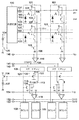
図1のブロック図により実施例1のADCを有する固体撮像装置の回路構成例を説明する。
[Circuit configuration]
A circuit configuration example of the solid-state imaging device having the ADC of the first embodiment will be described with reference to the block diagram of FIG.
画素101は、光電変換により、入射光に基づくアナログ信号を生成する。なお、図1は二行二列の画素101を有するエリアセンサの構成例を示している。
The
画素101において、フォトダイオード(PD)102は、光電変換により入射光量を電荷量に変換する光電変換部である。転送トランジスタ103のソースはPD102に、ゲートは転送制御線132に、ドレインはフローティングディフージョン領域(以下、FD領域)104にそれぞれ電気的に接続される。なお、FD領域104は、PD102から転送トランジスタ103を介して転送された電荷を保持する領域である。
In the
リセットトランジスタ105のソースはFD領域104に、ゲートはリセット制御線131に、ドレインは電源電圧にそれぞれ電気的に接続される。増幅トランジスタ106のゲートはFD領域104に、ドレインは電源電圧に、ソースはセレクトトランジスタ107のドレインにそれぞれ電気的に接続される。セレクトトランジスタ107のゲートはセレクト制御線133に、ソースは垂直信号線108に、ドレインは増幅トランジスタ106のソースにそれぞれ電気的に接続される。
The source of the
増幅トランジスタ106は、そのゲート部であるFD領域104に保持された電荷量に基づくアナログ信号を、セレクトトランジスタ107を介して垂直信号線108に増幅出力する。リセット制御線131、転送制御線132、および、セレクト制御線133はそれぞれ行選択部130に電気的に接続される。
The
負荷トランジスタ109は、そのドレインが垂直信号線108に電気的に接続され、垂直信号線108に定電流を流す定電流源として動作する。負荷トランジスタ109のゲートとトランジスタ135のゲートは電気的に接続され、両トランジスタのソースはともにグランド電圧に接続され、カレントミラー回路を形成する。トランジスタ135のゲートおよびドレインと電源電圧の間には定電流源134が電気的に接続される。
The drain of the
コンパレータ110の非反転入力端子(以下、+端子)は垂直信号線108に、反転入力端子(以下、−端子)は詳細を後述する第一ランプ基準電圧140にそれぞれ電気的に接続される。コンパレータ110は、+端子の電圧V+と−端子の電圧V-を比較して、電圧V+が電圧V-よりも高い(V+>V-)場合、信号線120にハイレベルHの電圧を出力する。また、V+≦V-の場合、信号線120にローレベルLの電圧を出力する。
The non-inverting input terminal (hereinafter referred to as “+” terminal) of the
ステートマシン129は、詳細は後述するが、信号線120に電気的に接続してコンパレータ110の出力を入力し、さらに制御パルス141と142を入力し、信号121、122、123を出力する。なお、信号122と123は反転の関係にある。
As will be described in detail later, the
トランジスタ136のゲートとトランジスタ111のゲートは電気的に接続され、両トランジスタのソースはともに電源電圧に接続され、カレントミラー回路を形成する。トランジスタ136のゲートおよびドレインとグランド電圧の間には定電流源137が電気的に接続される。
The gate of the
スイッチ112はゲートに入力される信号122によってオンオフし、スイッチ113はゲートに入力される信号123によってオンオフし、スイッチ114はゲートに入力される信号121によってオンオフする。静電容量116は、スイッチ112とスイッチ114の接続点とグランド電圧の間に電気的に接続された静電容量である。
The
つまり、スイッチ112と113は、定電流源として動作するトランジスタ111のドレイン電流の供給先を静電容量116にするか、グランド電位にするかの切替部である。また、スイッチ114は、静電容量116に蓄えた電荷を放電するための機構である。つまり、静電容量116は、スイッチ114がオフの場合は電荷を蓄える(充電)か、蓄えた電荷を維持し、スイッチ114がオンの場合は蓄えた電荷をグランド電圧に放出(放電)する。
That is, the
なお、スイッチ113がオンの場合のトランジスタ111のドレイン電流の供給先はグランド電圧に限らず、トランジスタ111のドレイン電流を放出することができればよい。つまり、スイッチ113の出力側の接続先はグランド電圧に限らず、グランド電圧以外の固定電圧などの基準電位でもよいし、抵抗素子を介してグランド電圧や固定電圧に接続されていても構わない。また、定電流源としてのトランジスタ111を一つのトランジスタとして記載するが、例えばゲート接地回路を用いるとトランジスタ111のドレインソース間電圧VDSを一定に保つことができ、より安定した電流を供給することができる。
Note that the supply destination of the drain current of the
コンパレータ118の+端子は詳細を後述する第二ランプ基準電圧154に、−端子はスイッチ112、スイッチ114と静電容量116の接続点にそれぞれ電気的に接続される。+端子の電圧V+が−端子の電圧V-よりも高い(V+>V-)場合、コンパレータ118は後述するカウンタ回路151にハイレベルHの電圧を出力する。また、V+≦V-の場合、コンパレータ118はカウンタ回路151にローレベルLの電圧を出力する。
The + terminal of the
カウンタ150は、上位mビットのAD変換を行う第一の変換部(ADC)用のカウンタであり、パルス信号152をクロックとして入力し、信号121によってカウントの停止が制御される。つまり、第一のADCは、画素信号を第一のビット長のディジタル信号にAD変換する。
The
カウンタ151は、下位n-mビットのAD変換を行う第二の変換部(ADC)用のカウンタであり、パルス信号153をクロックとして入力し、コンパレータ118の出力によってカウントの停止が制御される。つまり、第二のADCは、画素信号から第一のビット長のディジタル信号に相当するアナログ信号を減算した結果のアナログ信号を第二のビット長のディジタル信号にAD変換する。
The
カウンタ150と151は、カウントのリセット制御やアップダウンカウントの切り替えなどの動作を行う等の機能を有するが、本発明とは直接関係がないため、その詳細説明を省略する。また、カウンタ150と151のカウント値を読み出すために、一般に水平走査回路などを用いるが、その詳細説明を省略する。
The
[固体撮像装置の駆動方法]
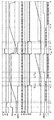
図2のタイミングチャートにより固体撮像装置の駆動方法を説明する。
[Driving method of solid-state imaging device]
A driving method of the solid-state imaging device will be described with reference to the timing chart of FIG.
図2において、信号presはリセット制御線131に印加される信号を、信号ptxは転送制御線132に印加される信号を、信号pselはセレクト制御線133に印加される信号をそれぞれ示す。信号Vlineは垂直信号線108の電圧を、信号COMPO1はコンパレータ110の出力信号の電圧を、信号COMPO2はコンパレータ118の出力信号の電圧をそれぞれ示す。信号VR1は第一基準電圧140を、信号VR2は第二ランプ基準電圧154をそれぞれ示す。信号CLK1はパルス信号152を、信号CLK2はパルス信号153をそれぞれ示す。
In FIG. 2, a signal pres indicates a signal applied to the
また、図1に示す制御パルス141、142は当該符号によって図2に示す。なお、制御パルス141、142、および、パルス信号152、153(CLK1、CLK2)は、図示しないタイミング発生器によって生成される。また、ステートマシン129によって生成される信号121、121、123も当該符号によって図2に示す。
Further, the
図1において、ハイレベル(以下、Hレベル)のパルス信号がゲートに印加されたトランジスタのソースとドレインの間が導通する(スイッチがオンになる)。一方、ローレベル(以下、Lレベル)のパルス信号がゲートに印加されたトランジスタのソースとドレインの間は電気的に遮断される(スイッチがオフになる)。勿論、Lレベルのパルス信号がゲートに印加されるとソースとドレインの間が導通するトランジスタを用いる場合、図2に示すパルス信号のHレベルとLレベルを逆転することで同様の動作が得られる。 In FIG. 1, conduction is established between the source and drain of a transistor to which a high-level (hereinafter, H-level) pulse signal is applied to the gate (the switch is turned on). On the other hand, the source and drain of a transistor to which a low level (hereinafter referred to as L level) pulse signal is applied to the gate is electrically disconnected (the switch is turned off). Of course, when using a transistor in which conduction between the source and drain is applied when an L level pulse signal is applied to the gate, the same operation can be obtained by reversing the H level and L level of the pulse signal shown in FIG. .
次に、図2のタイミングチャートにより時刻t0から順に固体撮像装置の駆動方法を説明する。 Next, a method for driving the solid-state imaging device will be described in order from time t0 with reference to the timing chart of FIG.
時刻t0において、データを読み出す行の信号pselがHレベルになり、図1に示す一行目の画素101が選択された状態になる。時刻t1において、画素101に印加する信号presをHレベルにしてFD領域104をリセットレベル(ほぼ電源電圧)にする。時刻t2において、信号presをLレベルにしてFD領域104のリセットを解除する。
At time t0, the signal psel for the row from which data is read becomes H level, and the
リセットトランジスタ105のソースとドレインの間が電気的に遮断される時に生じるチャージインジェクションによりFD領域104の電圧がリセットレベルより低下する。従って、増幅トランジスタ106が出力する信号の電圧が低下し、垂直信号線108の電圧Vlineも低下する。このとき、コンパレータ110の−端子に入力されるVR1(第一ランプ基準電圧140)は、リセットレベルよりも低い電圧に設定されていて、コンパレータ110はHレベルの信号COMPO1の出力を維持する。
Charge injection that occurs when the source and drain of the
時刻t3において、コンパレータ110の−端子に入力されるVR1の電圧は所定の傾きをもって上昇を開始し、第一のADC用のカウンタ150に対するCLK1(パルス信号152)の供給が開始される。なお、VR1のランプ開始時刻と、クロックCLK1の供給開始時刻をt3で揃える例を説明するが、両者の開始時刻をずらせばカウント値にオフセットを与えることが可能になる。
At time t3, the voltage V R1 input to the negative terminal of the
時刻t4において、コンパレータ110の−端子に入力されるVR1の電圧と、垂直信号線108を介して+端子に入力される電圧Vlineとの関係が逆転する。そのため、コンパレータ110が出力する信号COMPO1はHレベルからLレベルに変化する。なお、以下では、HレベルからLレベルへの変化を「H→L」、LレベルからHレベルへの変化を「L→H」と表記する。
At time t4, the relationship between the voltage V R1 input to the − terminal of the
COMPO1がLレベルになると、ステートマシン129は、信号121を反転(H→L)し、第一のADC用のカウンタ150のカウントが停止する。その結果、時刻t3からt4までのカウント結果が第一のADC用のカウント値として保持される。さらに、信号121の反転(H→L)によってスイッチ114がオフになり、静電容量116の充電が開始される。このとき静電容量116に蓄積する電荷の増加(電圧の上昇)の傾きαは次式で表される。
α = dV/dt = d(Q/C)/dt = I(t)/C1 …(2)
ここで、Iは充電電流、
C1は静電容量116のキャパシタンス。
When COMPO1 becomes L level, the
α = dV / dt = d (Q / C) / dt = I (t) / C1… (2)
Where I is the charging current,
C1 is the capacitance of
式(2)において、充電電流Iは定電流であり、時間に関係なく一定I(t)=Iと見做せる。 In the equation (2), the charging current I is a constant current and can be regarded as constant I (t) = I regardless of time.
時刻t5において、制御パルス141の立ち上がりで信号122が反転(H→L)し、信号123が反転(L→H)して、スイッチ112がオフ、スイッチ113がオンになり、静電容量116の充電が停止される。従って、傾きαで上昇した静電容量116の電圧の上昇は停止し、充電停止時の電圧が保持される(図2に破線で示す)。
At time t5, the
時刻t5は、ステートマシン129が、時刻t4以降に、制御パルス141のHレベルを検知したタイミングである。このタイミングに関しては、ステートマシン129の説明とともに後述する。また、時刻t4からt5までの期間Aを「充電期間」と呼ぶ。
Time t5 is timing when the
また、時刻t5において、信号123によりスイッチ113がオンになり、電流Iはスイッチ113を介してグランド電位へ放出される。言い替えれば、スイッチ112と113の切り替えにより、トランジスタ111から供給される定電流の接続先が静電容量116からグランド電位に変更される。この動作により、時刻t5以降もトランジスタ111から供給される定電流は遮断されることなく、常に流れ続ける。言い替えれば、スイッチ112と113による切り替え機構によって、定電流源の接続先を切り替えるため、静電容量116の充電期間が終了した後も、定電流源が供給する電流が停止されることはない。その結果、各列における充電期間の終了前後の電流変動が生じず、トランジスタ111は安定した電流を供給することができる。
At time t5, the
仮に切り替え機構がなく、時刻t5においてスイッチ112がオフし、定電流源が供給する電流が停止された場合、先に述べた理由より、他の列の電圧増加の傾きαが変化する。傾きαが変化すれば、第二のADCの変換結果が変動することになり、AD変換誤差が発生する。
If there is no switching mechanism and the
このように、本実施例においては、切り替え機構を用いて、静電容量116の充電後、定電流を放出して、定電流を安定に保つことができる。仮に列の中央において電源電圧の低下によりトランジスタ111のゲートソース間電圧VGSが変動し、列の中央において、トランジスタ111が供給する電流Iの値が低下したとする。しかし、トランジスタ111が供給する電流Iの値は、定電容量116の充電期間の終了前後において変動することはない。このため、電流Iの低下量は一定であり、補正が容易になり、AD変換誤差を低減することができる。
Thus, in this embodiment, the constant current can be released and the constant current can be kept stable after charging the
時刻t6において、第一のADCによるAD変換が終了し(第一のAD変換結果)、VR1(第一ランプ基準電圧140)の増加が停止し、カウンタ150に供給されるクロックCLK1も停止する。時刻t7において、第二のADC用のVR2(第二ランプ基準電圧154)が所定の傾きで上昇を開始し、第二のADC用のカウンタ151に対するCLK2(パルス信号153)の供給が開始される。
At time t6, AD conversion by the first ADC is completed (first AD conversion result), the increase in V R 1 (first ramp reference voltage 140) is stopped, and the clock CLK1 supplied to the
カウンタ151は、VR2の上昇開始(時刻t7)から、VR2が静電容量116が保持する電圧よりも高くなる(COMPO2がL→Hになる時刻t8)までの期間Bをカウントする(第二のAD変換結果)。このように、第一のADCによるAD変換の差分値を、第二のADCによるAD変換として行うことで、AD変換の分解能を上げることが可能になる。
充電期間(期間A)は、期間Bに対して短く、AD変換としてカウントを計測することが難しい。これに対して、期間Bは、期間Aよりも長く、AD変換としてカウントを計測すること容易である。また、CLK2(パルス信号153)の周波数を上げて、第二のADCにおけるAD変換の分解能を上げてもよい。 The charging period (period A) is shorter than the period B, and it is difficult to measure the count as AD conversion. On the other hand, the period B is longer than the period A, and it is easy to measure the count as AD conversion. In addition, the resolution of AD conversion in the second ADC may be increased by increasing the frequency of CLK2 (pulse signal 153).
時刻t9において、VR2の上昇が終了し、第二のADCによるAD変換が終了する。このタイミングでCLK2を停止する。同時に、制御パルス142をHレベルにして、ステートマシン129の状態を初期状態にリセットする。
At time t9, the increase in V R 2 ends and AD conversion by the second ADC ends. At this timing, CLK2 is stopped. At the same time, the
時刻t10において、ステートマシン129をリセットする制御パルス142をLレベルにし、信号ptxをL→Hにする。これにより、PD102で生じた電荷がFD領域104に転送される。FD領域104に保持された電荷に基づき、増幅トランジスタ106が出力する信号(以下、光電変換信号)が垂直信号線108に伝送される。FD領域104に保持された電荷に応じて、垂直信号線108の電圧Vlineは低下する。PD102の光電変換は、前回の信号読出期間において信号ptxがH→Lになった時刻t11から、今回の信号読出期間の時刻t10までの間に行われればよい。
At time t10, the
時刻t11において、信号ptxをH→Lにして、PD102とFD領域104を電気的に遮断する。この後、PD102で生じた電荷に基づく信号レベルを読み出し、t3〜t9と同様に、t12〜t18までの動作によりAD変換を行う。t12〜t18の動作は、前述したt3〜t9までの動作と同様であり、その詳細説明を省略する。
At time t11, the signal ptx is changed from H to L, and the
このようにして、リセットレベルのAD変換と、信号レベルのAD変換を行い、両者の差分することで相関二重サンプリング(CDS)動作を実現する。この相関二重サンプリング動作は、例えばノイズレベルの変換(N変換)時にダウンカウント、信号レベルの変換(S変換)時にアップカウントを行ってもよい。また、上記では、列ごとにカウンタ150、151を用いる例を示したが、共通のカウンタを用いて、各列でそのカウント値をリセット保持用のメモリ、信号保持用のメモリに保持し、差分をとる方式を用いてもよい。
In this way, the AD conversion at the reset level and the AD conversion at the signal level are performed, and a correlated double sampling (CDS) operation is realized by the difference between the two. In this correlated double sampling operation, for example, down-counting may be performed during noise level conversion (N conversion), and up-counting may be performed during signal level conversion (S conversion). In the above example, the
また、垂直信号線108を直接コンパレータ110の+端子に接続する構成例を示した。しかし、垂直信号線108とコンパレータ110の間に、列ごとに、ゲインアンプを配置して、ノイズレベルおよび光電変換レベル(信号レベル)を増幅した後、コンパレータ110の+端子に供給してもよい。
In addition, a configuration example in which the
また、コンパレータ118の出力COMPO2をステートマシン129とは別のステートマシンに接続し、第三の変換部(ADC)を用いることで第三のAD変換を行えば、AD変換の分解能さらに向上させることができる。つまり、第三のADCは、第二のADCによるAD変換の後、画素信号から第一および第二のビット長に対応するアナログ信号を減算し、その減算結果のアナログ信号を第三のビット長にAD変換する。
Also, if the output COMPO2 of the
[ステートマシン]
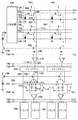
図3のブロック図によりステートマシン129の構成例を説明する。ステートマシン129は、バッファ301、インバータ302、フリップフロップ303を有する。
[State machine]
A configuration example of the
フリップフロップ303のクロック入力端子には制御パルス141が、非同期リセット端子には制御パルス142が、D端子にはコンパレータ110の出力信号120(COMPO1)がそれぞれ入力される。従って、フリップフロップ303は、信号COMPO1がLレベルになると、制御パルス141の立ち上がりに同期してLレベルの信号122を出力する。インバータ302は、信号122を反転した信号123を出力する。また、バッファ301は、信号COMPO1を信号121として出力する。信号121は、制御パルス141には同期されない。つまり、制御パルス141は、第一のADCを構成するステートマシン129の動作クロックとして機能する。
The
このように、過度的な電源電圧の変動による電流変動の影響を受け難く、精度が高いAD変換を実現することができる。 In this way, it is possible to realize AD conversion that is hardly affected by current fluctuation due to excessive fluctuation of the power supply voltage and that is highly accurate.
以下、本発明にかかる実施例2のADCを有する固体撮像装置およびその駆動方法を説明する。なお、実施例2において、実施例1と略同様の構成については、同一符号を付して、その詳細説明を省略する。 Hereinafter, a solid-state imaging device having an ADC according to a second embodiment of the present invention and a driving method thereof will be described. Note that the same reference numerals in the second embodiment denote the same parts as in the first embodiment, and a detailed description thereof will be omitted.
図4のブロック図により実施例2におけるステートマシン129を構成例を説明する。
A configuration example of the
実施例2におけるステートマシン129には、フリップフロップ304が追加されている。フリップフロップ303は、信号COMPO1がLレベルになり、制御パルス141が立ち上がるとLレベルの信号を出力する。フリップフロップ304は、フリップフロップ303の出力がLレベルになり、制御パルス141が立ち上がるとLレベルの信号122を出力する。つまり、信号COMPO1がLレベルになり、制御パルス141の二回分の立ち上がりを経て、制御信号141に同期したLレベルの信号122とHレベルの信号123が出力される。
A flip-
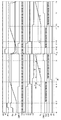
図5のタイミングチャートにより実施例2の固体撮像装置の駆動方法を説明する。 A driving method of the solid-state imaging device according to the second embodiment will be described with reference to the timing chart of FIG.
静電容量116の充電期間(期間A)は、信号121が立ち下り、信号122が立ち下がるまでの期間である。実施例2において期間Aは、制御パルス141の周期に換算すると、最小でも一周期より長く、最大で二周期を僅かに超える期間になる。
The charging period (period A) of the
充電期間は、スイッチ114のオフにより開始されるが、スイッチ114のオフ直後は信号121がH→Lになったことによる電圧変動の影響などを受けて、トランジスタ111が供給する電流がばらつく可能性がある。しかし、制御パルス141の一周期の間に当該電流が安定すれば第二のADCにおけるAD変換誤差にはならない。仮に、制御パルス141の一周期の間に当該電流が安定しない場合、ステートマシン129にフリップフロップをもう一つ追加して、期間Aを制御パルス141の二周期以上にすればよい。
The charging period starts when the
このように、静電容量116の充電期間の最小値を所定期間以上に制御して、充電開始時のトランジスタ111が供給する電流の変動が安定するまで充電期間を伸ばすことで、変動期間分をオフセット分として除去することができる。それにより、AD変換精度が向上する。
In this way, by controlling the minimum value of the charging period of the
また、静電容量116の充電期間の最小を制御パルス141の一周期以上にすることで、約一周期分のオフセット充電量が発生し、これは第二のADCのAD変換結果のオフセットになる。しかし、このオフセット充電量は、リセットレベルのAD変換においても、信号レベルのADの変換においても、同様に、オフセット充電量であり、前述したCDS動作により削除することができる。
Also, by setting the minimum charging period of the
以下、本発明にかかる実施例3のADCを有する固体撮像装置およびその駆動方法を説明する。なお、実施例3において、実施例1、2と略同様の構成については、同一符号を付して、その詳細説明を省略する。 Hereinafter, a solid-state imaging device having an ADC according to a third embodiment of the present invention and a driving method thereof will be described. Note that the same reference numerals in the third embodiment denote the same parts as in the first and second embodiments, and a detailed description thereof will be omitted.
図6のブロック図により実施例3のADCを有する固体撮像装置の回路構成例を説明する。実施例3の構成は、図1の構成に加えて、ゲートに制御パルス124が入力され、ドレインがスイッチ113のソースに、ソースがグランド電位にそれぞれ電気的に接続されたスイッチ115を有する。さらに、スイッチ115とスイッチ113の接続点とグランド電位の間に電気的に接続された静電容量117を有する。なお、制御パルス124は、図示しないタイミングジェネレータによって生成される。
A circuit configuration example of the solid-state imaging device having the ADC of the third embodiment will be described with reference to the block diagram of FIG. The configuration of the third embodiment includes a
つまり、実施例3の切り替え機構は、スイッチのオンオフによって、トランジスタ111が供給する電流の供給先を、静電容量116(第一の静電容量)と静電容量1117(第二の静電容量)の間で切り替える。
That is, according to the switching mechanism of the third embodiment, the supply destination of the current supplied by the
また、コンパレータ118の+端子は、実施例1におけるVR2(第二ランプ基準電圧154)の代わりに、スイッチ115と静電容量117の接続点に電気的に接続される。
Further, the + terminal of the
図7のタイミングチャートにより実施例3の固体撮像装置の駆動方法を説明する。 A method for driving the solid-state imaging device according to the third embodiment will be described with reference to the timing chart of FIG.
時刻t0〜t4の期間は、実施例1と同じ動作であり、その詳細説明を省略する。 The period from time t0 to t4 is the same as that in the first embodiment, and a detailed description thereof is omitted.
時刻t5において、制御パルス141の立ち上がりで信号122が反転(H→L)し、信号123が反転(L→H)して、スイッチ112がオフ、スイッチ113がオンになり、静電容量116の充電が停止される。従って、傾きαで上昇した静電容量116の電圧Vc1の上昇は停止し、充電停止時の電圧Vc1が保持される(図7の破線のVcとして示す)。
At time t5, the
なお、時刻t5は、ステートマシン129が、時刻t4以降に、制御パルス141のHレベルを検知したタイミングであるが、このタイミングの詳細は実施例1で説明したとおりである。また、時刻t4からt5までの期間Aを「第一の充電期間」と呼ぶ。
Note that time t5 is the timing at which the
また、時刻t5において、実施例3においては、信号123によりスイッチ113がオンになる。つまり、実施例3の切り替え機構により、トランジスタ111が供給する電流の供給先が第一の容量側から第二の容量側へ変更される。ただし、この時点では、制御パルス124がHレベルのため、スイッチ115はオンであり、電流Iによって第二の静電容量は充電されることなく、スイッチ115を介してグランド電位に放出される。つまり、電流Iは、二つのスイッチ113と115を介してグランド電位に放出される。この動作により、時刻t5以降もトランジスタ111から供給される定電流は遮断されることなく、常に流れ続ける。言い替えれば、スイッチ112、113、115による切り替え機構によって、定電流源の接続先を切り替えるため、第一の静電容量の充電期間が終了した後も、定電流源が供給する電流が停止されることはない。その結果、各列における充電期間の終了前後の電流変動が生じず、トランジスタ111は安定した電流を供給することができる。
At time t5, in the third embodiment, the
時刻t6において、第一のADCによるAD変換が終了し(第一のAD変換結果)、VR1(第一ランプ基準電圧140)の増加が停止し、カウンタ150に供給されるクロックCLK1も停止する。
At time t6, AD conversion by the first ADC is completed (first AD conversion result), the increase in V R 1 (first ramp reference voltage 140) is stopped, and the clock CLK1 supplied to the
時刻t7において、制御パルス124がL→Hに変化してスイッチ115がオフになり、第二の静電容量の充電が開始される(図7に実線のVcとして示す)。なお、第二の静電容量の充電により、画素の列ごとに独立したランプ基準電圧VR2が生成される。第一の静電容量116の電圧上昇の傾きαと、第二の静電容量117の電圧上昇の傾きβの間には次の関係が成り立つ。
β = I(t)/C2 = C1・α/C2 = α・C1/C2 …(3)
ここで、C1は第一の静電容量116のキャパシタンス、
C2は第二の静電容量117のキャパシタンス。
At time t7, the
β = I (t) / C2 = C1 ・ α / C2 = α ・ C1 / C2… (3)
Where C1 is the capacitance of the
C2 is the capacitance of the
例えば、キャパシタンスの比C1:C2が1:4だとすると、第一の充電期間(期間A)に対する第二の充電期間(t7〜t8の期間B)の関係は次式で表される。
A:B = C1:C2 = 1:4 …(4)
For example, assuming that the capacitance ratio C1: C2 is 1: 4, the relationship between the first charging period (period A) and the second charging period (period B from t7 to t8) is expressed by the following equation.
A: B = C1: C2 = 1: 4 (4)
つまり、この例では、第二の充電期間は、第一の充電期間の四倍になる。従って、第二の充電期間のカウントを第二のADCのAD変換として計測することで第二のAD変換として2ビットのAD変換を行うことができる。一方、第一の充電期間は、第二の充電期間に対して短く、AD変換としてカウントを計測することが難しい。 That is, in this example, the second charging period is four times the first charging period. Therefore, by measuring the count of the second charging period as AD conversion of the second ADC, 2-bit AD conversion can be performed as the second AD conversion. On the other hand, the first charging period is shorter than the second charging period, and it is difficult to measure the count as AD conversion.
勿論、第一の静電容量C1と第二の静電容量C2のキャパシタンス比を1:8や1:16などに変更して、第二の充電期間をさらに長くすることもできる。そうすれば、より精度が高い第二のADCによるAD変換が可能になり、第二のADCのビット数を上げることができる。 Of course, the second charging period can be further extended by changing the capacitance ratio of the first capacitance C1 and the second capacitance C2 to 1: 8, 1:16, or the like. Then, AD conversion by the second ADC with higher accuracy becomes possible, and the number of bits of the second ADC can be increased.
時刻t9以降の動作は、実施例1と同様であり、詳細説明を省略する。 The operation after time t9 is the same as that in the first embodiment, and detailed description thereof is omitted.
実施例3において、第二のADCのAD変換精度は、キャパシタンス比C1:C2によって決定する。これは、前述した式(2)(3)における傾きαとβの関係から明らかであり、トランジスタ111が供給する電流Iに依存しない。従って、AD変換精度は電流変動の影響を受け難く。このため、電流Iのばらつきを同じ電流Iでキャンセルすることができ、より精度の高いAD変換を行うことが可能になる。
In the third embodiment, the AD conversion accuracy of the second ADC is determined by the capacitance ratio C1: C2. This is apparent from the relationship between the slopes α and β in the above-described equations (2) and (3), and does not depend on the current I supplied from the
一般に、半導体の製造においては、トランジスタのIdのばらつきよりも、静電容量の相対精度の方がばらつきを小さくすることができる。この点を考慮しても精度の高いAD変換が可能になる。さらに、静電容量の相対精度は、一般に、トランジスタのIdばらつきよりも電源電圧や温度に関する変動が小さく、動作条件の違いによる変動が小さいAD変換が可能になる。 In general, in the manufacture of semiconductors, the variation in relative accuracy of capacitance can be made smaller than the variation in Id of transistors. Even if this point is taken into consideration, highly accurate AD conversion becomes possible. Furthermore, the relative accuracy of the capacitance generally has a smaller variation with respect to the power supply voltage and temperature than the variation in Id of the transistor, and AD conversion with a small variation due to a difference in operating conditions becomes possible.
[変形例]
図6に示す構成に、図4に示す構成のステートマシン129を適用することが可能である。図8のタイミングチャートにより変形例の固体撮像装置の駆動方法を説明する。
[Modification]
The
このような構成によれば、実施例2と同様に、第一の静電容量の第一の充電期間(期間A)は、信号121が立ち下り、信号122が立ち下がるまでの期間である。従って、第一の充電期間は、制御パルス141の周期に換算すると、最小でも一周期より長く、最大で二周期を僅かに超える期間になる。
According to such a configuration, as in the second embodiment, the first charging period (period A) of the first capacitance is a period until the
つまり、第二の静電容量を用いる方式においても、第一の充電期間の最小値を所定期間以上に制御して、充電開始時のトランジスタ111が供給する電流の変動が安定するまで充電期間を伸ばすことで、変動期間分をオフセット分として除去することができる。それにより、AD変換精度が向上する。
That is, even in the method using the second capacitance, the charging period is set until the fluctuation of the current supplied by the
以下、本発明にかかる実施例4のADCを有する固体撮像装置およびその駆動方法を説明する。なお、実施例4において、実施例1-3と略同様の構成については、同一符号を付して、その詳細説明を省略する。 Hereinafter, a solid-state imaging device having an ADC according to a fourth embodiment of the present invention and a driving method thereof will be described. Note that the same reference numerals in the fourth embodiment denote the same parts as in the first to third embodiments, and a detailed description thereof will be omitted.
図9のブロック図により実施例4のADCを有する固体撮像装置の回路構成例を説明する。実施例4の構成は、図6の構成に加えて、トランジスタ111が供給する電流を切り替える構成(電流の制御部)を有する。
A circuit configuration example of the solid-state imaging device having the ADC of the fourth embodiment will be described with reference to the block diagram of FIG. The configuration of the fourth embodiment has a configuration (current control unit) that switches the current supplied from the
トランジスタ401は、ドレインとゲートが定電流源402に、ソースが電源電圧にそれぞれ電気的に接続されている。制御パルス410がゲートに印加されるスイッチ403は、制御パルス410がLレベルの場合にソースとドレインの間が導通(オン)する。スイッチ403がオン状態において、トランジスタ401とトランジスタ136は一つのトランジスタと見做すことができる。また、スイッチ403がオフ状態において、トランジスタ401は、トランジスタ136とトランジスタ111が構成する回路から切り離される。
The
トランジスタ404は、ドレインとゲートが定電流源405に、ソースが電源電圧にそれぞれ電気的に接続されている。制御パルス411がゲートに印加されるスイッチ406は、制御パルス411がLレベルの場合にソースとドレインの間が導通(オン)する。スイッチ406がオン状態において、トランジスタ404とトランジスタ401は一つのトランジスタと見做すことができる。また、スイッチ403がオフ状態において、トランジスタ404は、トランジスタ401が構成する回路から切り離される。なお、制御パルス410、411は、図示しないタイミング発生器により発生される。
The
例えば、トランジスタ401とトランジスタ136のサイズ比を3:1、定電流源402と定電流源137の電流比を3:1とする。さらに、スイッチ403がオンのときにカレントミラーを形成する回路に流れる電流をI2、スイッチ403がオフのときに流れる電流をI1とする。この場合の電流値の比は下式で表される。
I1:I2 = 1:4 …(5)
For example, the size ratio between the
I1: I2 = 1: 4 (5)
例えば、トランジスタ404とトランジスタ136のサイズ比を4:1、定電流源405と定電流源137の電流比を4:1とする。さらに、スイッチ403とスイッチ406がオンのときにカレントミラーを形成する回路に流れる電流をI3、スイッチ403とスイッチ406がオフのときに流れる電流をI1とする。この場合の電流値の比は下式で表される。
I1:I3 = 1:8 …(6)
For example, the size ratio of the
I1: I3 = 1: 8 (6)
つまり、スイッチ403のオンオフ、さらにスイッチ406のオンオフによりトランジスタ111が供給する電流を制御して所定の電流値の比率を有するI1、I2またはI3に切り替えることができる。
That is, the current supplied from the
図10のタイミングチャートにより実施例4の固体撮像装置の駆動方法を説明する。 A driving method of the solid-state imaging device according to the fourth embodiment will be described with reference to the timing chart of FIG.
時刻t0からt20において、制御パルス411はHレベル(スイッチ406がオフ)、制御パルス410はLレベル(スイッチ403がオン)であり、トランジスタ111が供給する電流はI2である。第一のADCによるAD変換が終了した後の時刻t20において制御パルス410をL→Hにすると、トランジスタ111が供給する電流はI1になり、上記の比率に従えばトランジスタ111が供給する電流は1/4に減少する。第一の充電期間(期間A)における電圧の上昇率αと、第二の充電期間(期間B)における電圧の上昇率βの関係は下式で示される。
α = dVc1/dt = d(Q/C)/dt = I2(t)/C1
β = I1(t)/C2 = I2(t)/4C2 = αC1/4C2
ここで、C1:C2=1:1とすると、
β = α/4 …(7)
ここで、C1は第一の静電容量116のキャパシタンス、
C2は第二の静電容量117のキャパシタンス。
From time t0 to t20, the
α = dVc1 / dt = d (Q / C) / dt = I2 (t) / C1
β = I1 (t) / C2 = I2 (t) / 4C2 = αC1 / 4C2
Here, if C1: C2 = 1: 1,
β = α / 4 (7)
Where C1 is the capacitance of the
C2 is the capacitance of the
さらに、図10に破線で示すように、時刻t0からt20の期間における制御パルス411をLレベルにすると、時刻t0からt20において、トランジスタ111が供給する電流はI3になる。そして、時刻t20において制御パルス411もL→Hにすると、トランジスタ111が供給する電流はI1になり、上記の比率に従えばトランジスタ111が供給する電流は1/8に減少する。この場合のαとβの関係は下式で表される。
β = α/8 …(8)
ただし、C1:C2=1:1。
Further, as indicated by a broken line in FIG. 10, when the
β = α / 8 (8)
However, C1: C2 = 1: 1.
つまり、トランジスタ111が供給する電流を制御することにより、第一の充電期間に比べて第二の充電期間の長さを所定倍(上記では四または八倍)に制御することができる。例えば、撮影モードに応じてトランジスタ111が供給する電流を制御して、AD変換精度を変更することが可能になる。
In other words, by controlling the current supplied by the
実施例1と同様に、第二の充電期間のカウントを第二のADCによるAD変換として計測することにより、第二のADCによるAD変換として2ビットのAD変換を行うことができる。第二の充電期間は第一の充電期間よりも長いため、AD変換としてカウントすることが可能になる。 Similarly to the first embodiment, by measuring the count of the second charging period as AD conversion by the second ADC, 2-bit AD conversion can be performed as AD conversion by the second ADC. Since the second charging period is longer than the first charging period, it can be counted as AD conversion.
また、実施例4によれば、第二のADCのAD変換精度は電流比I1:I2(またはI1:I3)で決定する。そして電流比を生成する回路は列回路ではなく、先述した配線抵抗による電源電圧の低下の影響を受け難い。従って、ゲートソース間電圧VGSを一定に保つことが容易で安定した電流比が得られる。また、過度的な電源電圧の変動による電流ばらつきに関しても、第一の充電期間と第二の充電期間の切り替えタイミングt20のみの発生に限られる。 According to the fourth embodiment, the AD conversion accuracy of the second ADC is determined by the current ratio I1: I2 (or I1: I3). The circuit that generates the current ratio is not a column circuit, and is not easily affected by the power supply voltage drop caused by the wiring resistance described above. Therefore, it is easy to keep the gate-source voltage V GS constant, and a stable current ratio can be obtained. Further, the current variation due to the excessive power supply voltage variation is limited to the occurrence of only the switching timing t20 between the first charging period and the second charging period.
このように、電流ばらつきの影響を受け難い第二のADCによるAD変換を行うことができる上、解像度の必要性に応じて第二のADCによるAD変換の分解能を切り替えることができる。 As described above, AD conversion by the second ADC which is hardly affected by current variation can be performed, and the resolution of AD conversion by the second ADC can be switched according to the necessity of resolution.
なお、実施例3では静電容量の比、実施例4では電流比によって、第一の充電期間と第二の充電期間の比を設定する例を示したが、これらを組み合わせて、充電期間の比を制御しても構わない。 In Example 3, the ratio of the first charging period and the second charging period are set according to the capacitance ratio, and in Example 4, the current ratio. The ratio may be controlled.
なお、トランジスタ136に対して、電流切替用のトランジスタ401と404を配置する例を示したが、電流切替用のトランジスタは列ごとに設けてもよい。これは、時刻t5において電流の供給先を切り替るときは電流変動が抑制されており、時刻t20で電流の供給先を切り替えるときは電源電圧の変動が生じるが、全列同時の動作のため、列ごとのばらつきにはらなないからである。
Although an example in which the
また、図10には、時刻t10において、制御パルス410をH→Lにする例を示したが、このタイミングはこの限りではない。リセットレベルの変換が終了し、光電変換レベルの変換が開始されるまでの期間、つまり時刻t9〜t12の間であれば何時でも構わない。
FIG. 10 shows an example in which the
Claims (8)
前記画素信号を第一のビット長のディジタル信号に変換する第一の変換を行う第一の変換部と、
前記画素信号から、前記第一のビット長のディジタル信号に相当するアナログ信号を減算した結果のアナログ信号を、第二のビット長のディジタル信号に変換する第二の変換を行う第二の変換部とを有し、
前記第二の変換部は、
電流源と、
第一の容量とを有し、
前記第一の変換の後、前記第一の容量に前記減算した結果のアナログ信号が充電され、前記第一の容量に充電された前記アナログ信号と基準電圧の比較に基づき前記第二の変換が行われ、
前記第一の変換の後、前記第二の変換を開始するまでの期間に、前記電流源が供給する電流により前記第一の容量を充電する期間は、前記第一の変換部の動作クロックの一周期以上であることを特徴とする固体撮像装置。 A pixel that outputs a pixel signal;
A first converter for performing a first conversion for converting the pixel signal into a digital signal having a first bit length;
A second conversion unit for performing a second conversion for converting an analog signal obtained by subtracting an analog signal corresponding to the digital signal having the first bit length from the pixel signal into a digital signal having a second bit length. And
The second converter is
A current source;
Having a first capacity,
After the first conversion, the analog signal as a result of the subtraction is charged to the first capacitor, and the second conversion is performed based on a comparison between the analog signal charged to the first capacitor and a reference voltage. Done,
After the first conversion, the period until the start of the second conversion, the period during which the current source to charge said first capacitor by the current supplied, the operation clock of the first conversion unit solid-state image sensor characterized in that at the one period or more.
前記第一の容量の充電後、前記電流源が供給する電流により前記第二の容量を充電することによって前記基準電圧が生成されることを特徴とする請求項1に記載された固体撮像装置。 The second conversion unit further has a second capacity,
2. The solid-state imaging device according to claim 1 , wherein the reference voltage is generated by charging the second capacitor with a current supplied from the current source after charging the first capacitor .
前記複数列の各々に、それぞれが対応して設けられ、前記画素信号を第一のビット長のディジタル信号に変換する複数の第一の変換部と、
前記複数の第一の変換部の各々に、それぞれが対応して設けられ、前記画素信号から、前記第一のビット長のディジタル信号に相当するアナログ信号を減算した結果のアナログ信号を、第二のビット長のディジタル信号に変換する複数の第二の変換部とを有し、
前記複数の第二の変換部の各々は、
電流源と、
第一の容量と、
第二の容量と、
前記第一の容量に接続された第一の入力端子及び前記第二の容量に接続された第二の入力端子を有する比較器とを有し、
前記複数の第一の変換部と前記複数の第二の変換部の各々において、
前記第一の変換部による前記画素信号の変換後、前記電流源が供給する電流により前記第一の容量を充電することによって、前記第二の変換部は、前記減算した結果のアナログ信号を生成し、
前記第一の容量の充電後、前記電流源が供給する電流により前記第二の容量を充電することによる基準電圧を前記第二の変換部が生成することで、前記複数の第二の変換部の各々において前記基準電圧が生成され、
前記複数の第二の変換部の各々が、前記減算した結果のアナログ信号と、前記基準電圧とを前記比較器で比較した結果に基づき当該アナログ信号を変換することを特徴とする固体撮像装置。 A plurality of pixels that output pixel signals, arranged over a plurality of columns;
A plurality of first converters provided corresponding to each of the plurality of columns and converting the pixel signal into a digital signal having a first bit length;
An analog signal obtained by subtracting an analog signal corresponding to the digital signal having the first bit length from the pixel signal is provided corresponding to each of the plurality of first conversion units. A plurality of second conversion units for converting into a digital signal having a bit length of
Each of the plurality of second conversion units is
A current source;
With the first capacity,
With a second capacity,
A comparator having a first input terminal connected to the first capacitor and a second input terminal connected to the second capacitor;
In each of the plurality of first conversion units and the plurality of second conversion units,
After the pixel signal is converted by the first conversion unit, the second conversion unit generates an analog signal as a result of the subtraction by charging the first capacitor with a current supplied by the current source. And
After the charging of the first capacitor, the second converter generates a reference voltage by charging the second capacitor with a current supplied by the current source, whereby the plurality of second converters The reference voltage is generated in each of
Each of said plurality of second conversion unit, the analog signal of the subtraction result, the solid-state image pickup you and converting the analog signal on the basis of the result of the said reference voltage are compared by the comparator apparatus.
前記固体撮像装置は、前記ゲート部をリセットしたリセットレベル、および、前記光電変換部で生じた電荷に基づく信号レベルを読み出し、前記リセットレベルと前記信号レベルを用いて相関二重サンプリング動作を行い、前記相関二重サンプリング動作において、前記第一の容量と前記第二の容量にともに充電された充電量のオフセットを減算することを特徴とする請求項3から請求項6の何れか一項に記載された固体撮像装置。 The pixel includes a photoelectric conversion unit, an amplification transistor that outputs a pixel signal based on charges generated in the photoelectric conversion unit, and a reset transistor that resets a gate unit of the amplification transistor,
The solid-state imaging device reads a reset level when the gate unit is reset, and a signal level based on charges generated in the photoelectric conversion unit, and performs a correlated double sampling operation using the reset level and the signal level, in the correlated double sampling operation, according to any one of claims 6 claim 3, characterized by subtracting said first capacitor and said second charge amount of offset both charged in the capacitor Solid-state imaging device.
Priority Applications (2)
| Application Number | Priority Date | Filing Date | Title |
|---|---|---|---|
| JP2012026421A JP5979896B2 (en) | 2012-02-09 | 2012-02-09 | Solid-state imaging device |
| US13/748,111 US8760337B2 (en) | 2012-02-09 | 2013-01-23 | Solid-state image sensing device |
Applications Claiming Priority (1)
| Application Number | Priority Date | Filing Date | Title |
|---|---|---|---|
| JP2012026421A JP5979896B2 (en) | 2012-02-09 | 2012-02-09 | Solid-state imaging device |
Publications (3)
| Publication Number | Publication Date |
|---|---|
| JP2013165341A JP2013165341A (en) | 2013-08-22 |
| JP2013165341A5 JP2013165341A5 (en) | 2015-03-12 |
| JP5979896B2 true JP5979896B2 (en) | 2016-08-31 |
Family
ID=48945147
Family Applications (1)
| Application Number | Title | Priority Date | Filing Date |
|---|---|---|---|
| JP2012026421A Expired - Fee Related JP5979896B2 (en) | 2012-02-09 | 2012-02-09 | Solid-state imaging device |
Country Status (2)
| Country | Link |
|---|---|
| US (1) | US8760337B2 (en) |
| JP (1) | JP5979896B2 (en) |
Families Citing this family (20)
| Publication number | Priority date | Publication date | Assignee | Title |
|---|---|---|---|---|
| JP6004685B2 (en) | 2012-03-19 | 2016-10-12 | キヤノン株式会社 | Solid-state imaging device and driving method thereof |
| US8581761B1 (en) * | 2012-10-12 | 2013-11-12 | Aptina Imaging Corporation | Methods and apparatus for performing code correction for hybrid analog-to-digital converters in imaging devices |
| JP6246004B2 (en) | 2014-01-30 | 2017-12-13 | キヤノン株式会社 | Solid-state imaging device |
| JP6274898B2 (en) * | 2014-02-17 | 2018-02-07 | キヤノン株式会社 | Solid-state imaging device and camera |
| JP6412328B2 (en) | 2014-04-01 | 2018-10-24 | キヤノン株式会社 | Solid-state imaging device and camera |
| JP6482186B2 (en) | 2014-05-23 | 2019-03-13 | キヤノン株式会社 | Imaging apparatus and driving method thereof |
| JP6351404B2 (en) | 2014-07-02 | 2018-07-04 | キヤノン株式会社 | Imaging apparatus and imaging system |
| WO2016031066A1 (en) | 2014-08-29 | 2016-03-03 | オリンパス株式会社 | Imaging device and imaging system |
| KR102261587B1 (en) | 2014-12-05 | 2021-06-04 | 삼성전자주식회사 | Image sensor for improving nonlinearty of low code region, method thereof, and device including the same |
| JP6480768B2 (en) | 2015-03-17 | 2019-03-13 | キヤノン株式会社 | Solid-state imaging device and driving method thereof |
| JP6877203B2 (en) | 2017-03-24 | 2021-05-26 | キヤノン株式会社 | Imaging device and moving object |
| US10834354B2 (en) | 2018-06-25 | 2020-11-10 | Canon Kabushiki Kaisha | Imaging device, imaging system, movable object, and signal processing device |
| JP7245014B2 (en) | 2018-09-10 | 2023-03-23 | キヤノン株式会社 | Solid-state imaging device, imaging system, and driving method for solid-state imaging device |
| JP7353752B2 (en) | 2018-12-06 | 2023-10-02 | キヤノン株式会社 | Photoelectric conversion device and imaging system |
| WO2020129238A1 (en) * | 2018-12-21 | 2020-06-25 | リコー電子デバイス株式会社 | Laser drive device |
| JP7303682B2 (en) | 2019-07-19 | 2023-07-05 | キヤノン株式会社 | Photoelectric conversion device and imaging system |
| JP7374639B2 (en) | 2019-07-19 | 2023-11-07 | キヤノン株式会社 | Photoelectric conversion device and imaging system |
| CN113141444B (en) * | 2020-01-19 | 2023-08-08 | Oppo广东移动通信有限公司 | Image sensor, imaging device, electronic apparatus, image processing system, and signal processing method |
| CN113497905B (en) | 2020-04-01 | 2024-03-12 | 佳能株式会社 | Photoelectric conversion apparatus, imaging system, and moving object |
| US11777515B2 (en) * | 2021-04-27 | 2023-10-03 | Novatek Microelectronics Corp. | Column analog-to-digital converter and local counting method thereof |
Family Cites Families (14)
| Publication number | Priority date | Publication date | Assignee | Title |
|---|---|---|---|---|
| JP3361005B2 (en) * | 1996-03-04 | 2003-01-07 | 株式会社東芝 | A / D conversion circuit and imaging device |
| US5801657A (en) * | 1997-02-05 | 1998-09-01 | Stanford University | Serial analog-to-digital converter using successive comparisons |
| JP3783892B2 (en) * | 1997-04-09 | 2006-06-07 | ソニー株式会社 | Digital analog converter |
| JP4033948B2 (en) * | 1997-08-07 | 2008-01-16 | 沖電気工業株式会社 | Color palette RAM and D / A converter |
| EP0952671B1 (en) * | 1998-04-24 | 2004-12-08 | Texas Instruments Incorporated | Pipeline analog-to-digital conversion system using a modified coding scheme and method of operation |
| JP4107269B2 (en) * | 2004-02-23 | 2008-06-25 | ソニー株式会社 | Solid-state imaging device |
| US7423790B2 (en) | 2004-03-18 | 2008-09-09 | Canon Kabushiki Kaisha | Photoelectric conversion apparatus and contact-type image sensor |
| JP4802767B2 (en) * | 2006-03-06 | 2011-10-26 | ソニー株式会社 | Analog-digital converter, solid-state imaging device using the same, and driving method thereof |
| JP4744343B2 (en) * | 2006-04-10 | 2011-08-10 | ソニー株式会社 | Solid-state imaging device and driving method of solid-state imaging device |
| JP2009033305A (en) * | 2007-07-25 | 2009-02-12 | Panasonic Corp | Solid-state imaging apparatus |
| JP4500862B2 (en) | 2008-04-11 | 2010-07-14 | キヤノン株式会社 | Driving method of solid-state imaging device |
| JP4891308B2 (en) | 2008-12-17 | 2012-03-07 | キヤノン株式会社 | Solid-state imaging device and imaging system using solid-state imaging device |
| JP5375277B2 (en) * | 2009-04-02 | 2013-12-25 | ソニー株式会社 | Solid-state imaging device, imaging device, electronic device, AD conversion device, AD conversion method |
| JP5562172B2 (en) | 2010-08-10 | 2014-07-30 | キヤノン株式会社 | Constant current circuit and solid-state imaging device using the same |
-
2012
- 2012-02-09 JP JP2012026421A patent/JP5979896B2/en not_active Expired - Fee Related
-
2013
- 2013-01-23 US US13/748,111 patent/US8760337B2/en not_active Expired - Fee Related
Also Published As
| Publication number | Publication date |
|---|---|
| US20130207825A1 (en) | 2013-08-15 |
| JP2013165341A (en) | 2013-08-22 |
| US8760337B2 (en) | 2014-06-24 |
Similar Documents
| Publication | Publication Date | Title |
|---|---|---|
| JP5979896B2 (en) | Solid-state imaging device | |
| JP5858695B2 (en) | Solid-state imaging device and driving method of solid-state imaging device | |
| US8760213B2 (en) | Ramp signal output circuit, analog-to-digital conversion circuit, imaging device, method for driving ramp signal output circuit, method for driving analog-to-digital conversion circuit, and method for driving imaging device | |
| US7315273B2 (en) | Analog-to-digital conversion method, analog-to-digital converter, semiconductor device for detecting distribution of physical quantity, and electronic apparatus | |
| US7567280B2 (en) | Solid-state imaging device, analogue-digital converting method in solid-state imaging device and imaging apparatus | |
| JP5893573B2 (en) | Solid-state imaging device | |
| JP4529834B2 (en) | Solid-state imaging device, driving method of solid-state imaging device, and imaging device | |
| JP4952301B2 (en) | Imaging device and camera | |
| US9060139B2 (en) | Solid-state imaging apparatus and method for driving the same | |
| JP2009033305A (en) | Solid-state imaging apparatus | |
| US9294701B2 (en) | Image pickup apparatus, method for driving image pickup apparatus, image pickup system, and method for driving image pickup system | |
| JP4770577B2 (en) | Solid-state imaging device | |
| JP6112871B2 (en) | Imaging device and imaging apparatus | |
| US11611336B2 (en) | Comparator for low-banding noise and CMOS image sensor including the same | |
| WO2016009866A1 (en) | Solid-state imaging element, da converter, sample-and-hold circuit, and electronic equipment |
Legal Events
| Date | Code | Title | Description |
|---|---|---|---|
| A521 | Request for written amendment filed |
Free format text: JAPANESE INTERMEDIATE CODE: A523 Effective date: 20150121 |
|
| A621 | Written request for application examination |
Free format text: JAPANESE INTERMEDIATE CODE: A621 Effective date: 20150121 |
|
| A977 | Report on retrieval |
Free format text: JAPANESE INTERMEDIATE CODE: A971007 Effective date: 20160125 |
|
| A131 | Notification of reasons for refusal |
Free format text: JAPANESE INTERMEDIATE CODE: A131 Effective date: 20160129 |
|
| A521 | Request for written amendment filed |
Free format text: JAPANESE INTERMEDIATE CODE: A523 Effective date: 20160328 |
|
| TRDD | Decision of grant or rejection written | ||
| A01 | Written decision to grant a patent or to grant a registration (utility model) |
Free format text: JAPANESE INTERMEDIATE CODE: A01 Effective date: 20160627 |
|
| A61 | First payment of annual fees (during grant procedure) |
Free format text: JAPANESE INTERMEDIATE CODE: A61 Effective date: 20160726 |
|
| R151 | Written notification of patent or utility model registration |
Ref document number: 5979896 Country of ref document: JP Free format text: JAPANESE INTERMEDIATE CODE: R151 |
|
| LAPS | Cancellation because of no payment of annual fees |