JP5978068B2 - Display device in electronic apparatus and control method thereof - Google Patents
Display device in electronic apparatus and control method thereof Download PDFInfo
- Publication number
- JP5978068B2 JP5978068B2 JP2012188540A JP2012188540A JP5978068B2 JP 5978068 B2 JP5978068 B2 JP 5978068B2 JP 2012188540 A JP2012188540 A JP 2012188540A JP 2012188540 A JP2012188540 A JP 2012188540A JP 5978068 B2 JP5978068 B2 JP 5978068B2
- Authority
- JP
- Japan
- Prior art keywords
- display
- memory
- storage element
- display device
- electronic device
- Prior art date
- Legal status (The legal status is an assumption and is not a legal conclusion. Google has not performed a legal analysis and makes no representation as to the accuracy of the status listed.)
- Active
Links
Images


Classifications
-
- G—PHYSICS
- G06—COMPUTING; CALCULATING OR COUNTING
- G06F—ELECTRIC DIGITAL DATA PROCESSING
- G06F1/00—Details not covered by groups G06F3/00 - G06F13/00 and G06F21/00
- G06F1/26—Power supply means, e.g. regulation thereof
- G06F1/32—Means for saving power
- G06F1/3203—Power management, i.e. event-based initiation of a power-saving mode
- G06F1/3234—Power saving characterised by the action undertaken
- G06F1/325—Power saving in peripheral device
- G06F1/3265—Power saving in display device
-
- G—PHYSICS
- G09—EDUCATION; CRYPTOGRAPHY; DISPLAY; ADVERTISING; SEALS
- G09G—ARRANGEMENTS OR CIRCUITS FOR CONTROL OF INDICATING DEVICES USING STATIC MEANS TO PRESENT VARIABLE INFORMATION
- G09G3/00—Control arrangements or circuits, of interest only in connection with visual indicators other than cathode-ray tubes
- G09G3/20—Control arrangements or circuits, of interest only in connection with visual indicators other than cathode-ray tubes for presentation of an assembly of a number of characters, e.g. a page, by composing the assembly by combination of individual elements arranged in a matrix no fixed position being assigned to or needed to be assigned to the individual characters or partial characters
-
- G—PHYSICS
- G06—COMPUTING; CALCULATING OR COUNTING
- G06F—ELECTRIC DIGITAL DATA PROCESSING
- G06F1/00—Details not covered by groups G06F3/00 - G06F13/00 and G06F21/00
- G06F1/26—Power supply means, e.g. regulation thereof
-
- G—PHYSICS
- G09—EDUCATION; CRYPTOGRAPHY; DISPLAY; ADVERTISING; SEALS
- G09G—ARRANGEMENTS OR CIRCUITS FOR CONTROL OF INDICATING DEVICES USING STATIC MEANS TO PRESENT VARIABLE INFORMATION
- G09G3/00—Control arrangements or circuits, of interest only in connection with visual indicators other than cathode-ray tubes
- G09G3/04—Control arrangements or circuits, of interest only in connection with visual indicators other than cathode-ray tubes for presentation of a single character by selection from a plurality of characters, or by composing the character by combination of individual elements, e.g. segments using a combination of such display devices for composing words, rows or the like, in a frame with fixed character positions
-
- H—ELECTRICITY
- H04—ELECTRIC COMMUNICATION TECHNIQUE
- H04N—PICTORIAL COMMUNICATION, e.g. TELEVISION
- H04N21/00—Selective content distribution, e.g. interactive television or video on demand [VOD]
- H04N21/40—Client devices specifically adapted for the reception of or interaction with content, e.g. set-top-box [STB]; Operations thereof
- H04N21/41—Structure of client; Structure of client peripherals
- H04N21/422—Input-only peripherals, i.e. input devices connected to specially adapted client devices, e.g. global positioning system [GPS]
- H04N21/42204—User interfaces specially adapted for controlling a client device through a remote control device; Remote control devices therefor
-
- H—ELECTRICITY
- H04—ELECTRIC COMMUNICATION TECHNIQUE
- H04N—PICTORIAL COMMUNICATION, e.g. TELEVISION
- H04N21/00—Selective content distribution, e.g. interactive television or video on demand [VOD]
- H04N21/40—Client devices specifically adapted for the reception of or interaction with content, e.g. set-top-box [STB]; Operations thereof
- H04N21/43—Processing of content or additional data, e.g. demultiplexing additional data from a digital video stream; Elementary client operations, e.g. monitoring of home network or synchronising decoder's clock; Client middleware
- H04N21/443—OS processes, e.g. booting an STB, implementing a Java virtual machine in an STB or power management in an STB
- H04N21/4436—Power management, e.g. shutting down unused components of the receiver
-
- H—ELECTRICITY
- H04—ELECTRIC COMMUNICATION TECHNIQUE
- H04N—PICTORIAL COMMUNICATION, e.g. TELEVISION
- H04N21/00—Selective content distribution, e.g. interactive television or video on demand [VOD]
- H04N21/40—Client devices specifically adapted for the reception of or interaction with content, e.g. set-top-box [STB]; Operations thereof
- H04N21/47—End-user applications
-
- H—ELECTRICITY
- H04—ELECTRIC COMMUNICATION TECHNIQUE
- H04N—PICTORIAL COMMUNICATION, e.g. TELEVISION
- H04N5/00—Details of television systems
- H04N5/63—Generation or supply of power specially adapted for television receivers
-
- G—PHYSICS
- G09—EDUCATION; CRYPTOGRAPHY; DISPLAY; ADVERTISING; SEALS
- G09G—ARRANGEMENTS OR CIRCUITS FOR CONTROL OF INDICATING DEVICES USING STATIC MEANS TO PRESENT VARIABLE INFORMATION
- G09G2330/00—Aspects of power supply; Aspects of display protection and defect management
- G09G2330/02—Details of power systems and of start or stop of display operation
- G09G2330/021—Power management, e.g. power saving
-
- Y—GENERAL TAGGING OF NEW TECHNOLOGICAL DEVELOPMENTS; GENERAL TAGGING OF CROSS-SECTIONAL TECHNOLOGIES SPANNING OVER SEVERAL SECTIONS OF THE IPC; TECHNICAL SUBJECTS COVERED BY FORMER USPC CROSS-REFERENCE ART COLLECTIONS [XRACs] AND DIGESTS
- Y02—TECHNOLOGIES OR APPLICATIONS FOR MITIGATION OR ADAPTATION AGAINST CLIMATE CHANGE
- Y02D—CLIMATE CHANGE MITIGATION TECHNOLOGIES IN INFORMATION AND COMMUNICATION TECHNOLOGIES [ICT], I.E. INFORMATION AND COMMUNICATION TECHNOLOGIES AIMING AT THE REDUCTION OF THEIR OWN ENERGY USE
- Y02D10/00—Energy efficient computing, e.g. low power processors, power management or thermal management
-
- Y—GENERAL TAGGING OF NEW TECHNOLOGICAL DEVELOPMENTS; GENERAL TAGGING OF CROSS-SECTIONAL TECHNOLOGIES SPANNING OVER SEVERAL SECTIONS OF THE IPC; TECHNICAL SUBJECTS COVERED BY FORMER USPC CROSS-REFERENCE ART COLLECTIONS [XRACs] AND DIGESTS
- Y02—TECHNOLOGIES OR APPLICATIONS FOR MITIGATION OR ADAPTATION AGAINST CLIMATE CHANGE
- Y02D—CLIMATE CHANGE MITIGATION TECHNOLOGIES IN INFORMATION AND COMMUNICATION TECHNOLOGIES [ICT], I.E. INFORMATION AND COMMUNICATION TECHNOLOGIES AIMING AT THE REDUCTION OF THEIR OWN ENERGY USE
- Y02D30/00—Reducing energy consumption in communication networks
- Y02D30/50—Reducing energy consumption in communication networks in wire-line communication networks, e.g. low power modes or reduced link rate
Description
本発明は、視聴覚プログラムの受信機−デコーダ装置の分野に関し、より厳密には、スタンバイモードにおける表示管理に関する。 The present invention relates to the field of audiovisual program receiver-decoder devices, and more specifically to display management in standby mode.
視聴覚プログラムの受信機/デコーダは、ますます多くの機能をユーザに提供する。プログラムの受信、記録及び表示を目的とする必須機能に加えて、機器は、例えば、第3の装置との通信、設定、又は電子マネーのための多数のインターフェースを有する。例えば、テレビ受像機、コンピュータ、スケジュール管理用コンピュータソフト、携帯電話機、データ記憶装置、プリンタ等の家庭用デジタル製品の開発の高まりは、異なる家電への相互接続を可能にするようプログラム受信機のインターフェースの数も増大させる。 Audiovisual program receivers / decoders provide more and more functions to users. In addition to the essential functions for the purpose of receiving, recording and displaying the program, the device has a number of interfaces, for example for communication with a third device, settings or electronic money. For example, the development of home digital products such as television receivers, computers, schedule management computer software, mobile phones, data storage devices, printers, etc., program receiver interfaces to enable interconnection to different home appliances Increase the number of.
多数の装置及びインターフェースを有する構成は、ユーザが快適な機能の利益を享受することを可能にする一方で、回路の増大による高いエネルギ消費を引き起こす。故に、家庭用の装置のエネルギ消費並びに設置物全体及びより広くは家全体のエネルギ消費を制御することがますます重要になる。 A configuration having a large number of devices and interfaces allows the user to enjoy the benefits of comfortable functionality while causing high energy consumption due to increased circuitry. Therefore, it becomes increasingly important to control the energy consumption of household equipment and the energy consumption of the entire installation and more widely the whole house.
エネルギ消費に関して、現在、ヨーロッパの公式の指示が存在する。かかる公式の指示は、汎用の装置の設計段階で注意深く考慮されなければならない。 There are now official European directives on energy consumption. Such formal instructions must be carefully considered during the general equipment design phase.
エネルギ消費の高い削減制約は、装置を起動する必要性と結び付けられて、問題を生じる。最低限のエネルギ消費に対応するスタンバイモードを有することが必要であり、且つ、スタンバイモードにある装置を起動し得ることが必要である。これは、装置の起動を可能にするサブアセンブリがスタンバイモードにおいて依然として動作することを必要とする。 The high energy consumption reduction constraints are associated with the need to start the device and cause problems. It is necessary to have a standby mode corresponding to the minimum energy consumption, and it is necessary to be able to wake up a device in standby mode. This requires that the subassembly that allows device startup to still operate in standby mode.
その場合に、そのような制約を満たすという目的で、電源、マザーボード、並びにキーボード及びディスプレイ管理ボード(時々KDB(Key and Display Boardの略称)と呼ばれる。)を有するアーキテクチャを使用することが通例である。 In that case, it is customary to use an architecture having a power supply, a motherboard, and a keyboard and display management board (sometimes called KDB (abbreviation of Key and Display Board)) for the purpose of satisfying such constraints. .
なお、以下の記載において、「マザーボード」、「電源」及び「KDB」との称号は、必ずしも独立した電子ボードに対応するわけではなく、関連する機能に関与する全ての構成要素を示す。 In the following description, the designations “motherboard”, “power supply”, and “KDB” do not necessarily correspond to independent electronic boards, but indicate all components related to related functions.
従って、「マザーボード」は、KDBによってサポートされる機能及び電源によってサポートされるエネルギラインの供給と離れて装置によってサポートされる機能を果たす全ての電子回路を表す。 Thus, “motherboard” refers to all electronic circuits that perform the functions supported by the device apart from the functions supported by the KDB and the supply of energy lines supported by the power supply.
「KDB」は、スタンバイモードにおける制御ユニット機能に加えて、リモートコントロール受信、キーボード管理及び表示機能に対応する全ての回路を表す。しかし、それらの回路は、ここで「マザーボード」と呼ばれる全ての回路と同じ電子ボード上に設置されてよい。 “KDB” represents all circuits corresponding to remote control reception, keyboard management, and display functions in addition to the control unit functions in the standby mode. However, these circuits may be installed on the same electronic board as all the circuits referred to herein as “motherboards”.
同じように、装置が接続されている電気ネットワークからの電圧及び電流において様々な供給ラインが設けられることを可能にする電源回路は、ここで「マザーボード」と呼ばれる回路と同じボード上に設置されてよい。 Similarly, the power supply circuit, which allows various supply lines to be provided in the voltage and current from the electrical network to which the device is connected, is installed on the same board as the circuit referred to herein as the “motherboard”. Good.
ここで使用される称号は、当業者が、本発明が属する適用範囲内にある装置のアーキテクチャ全体をより良く理解することを可能にする。 The designations used herein allow those skilled in the art to better understand the overall architecture of the device within the scope to which the present invention belongs.
KDBは、リモートコントロールによる装置制御のためのデータ受信に必要な要素をサポートする。しかし、リモートコントロールは、例えばブルートゥースのような如何なる他のタイプの通信も使用することができる。 KDB supports elements necessary for data reception for device control by remote control. However, the remote control can use any other type of communication, for example Bluetooth.
マザーボード及びKDBに基づく当該アーキテクチャは、スタンバイモードにおいて、表示及びキーボード管理並びにリモートコントロールフレームの受信のためにKDBの電源供給及び動作を保つことによって、マザーボード又はマザーボード全体に存在する非常に多くの機能の電力供給を中断することが可能であり且つ容易であるので、エネルギの経済的な管理を可能にする。実際には、視聴覚プログラムを受信する装置がスタンバイモードにおいて設定される場合に、装置を起動して作動モードに戻すためにキーボード又はリモートコントロールを使用することが通例である。 The architecture based on the motherboard and KDB, in standby mode, keeps the power supply and operation of the KDB for display and keyboard management and reception of remote control frames, so that a large number of functions existing on the motherboard or the entire motherboard can be obtained. Since it is possible and easy to interrupt the power supply, it allows an economical management of energy. In practice, when a device receiving an audiovisual program is set in standby mode, it is customary to use a keyboard or remote control to wake up the device and return to operating mode.
スタンバイモードでは、例えば、時間のような他の情報とともに動作モード(スタンバイモード)をユーザに示すためにディスプレイを動作したままとすることも通例である。このモードにおいて、KDBは時々完全に自立しており、マザーボードは動作しておらず、表示メモリのコンテンツを更新するであろうソフトウェアアプリケーションを実施しない。 In the standby mode, it is also common to leave the display operating to show the user the operating mode (standby mode) along with other information such as time, for example. In this mode, the KDB is sometimes completely self-supporting, the motherboard is not running and does not implement software applications that will update the contents of the display memory.
このアーキテクチャに基づき設計される装置の設計における重要な制約は、実施上、費用上及びモジュール上の理由のために、KDBを可能な限り簡素化することである。 An important limitation in the design of devices designed based on this architecture is to simplify the KDB as much as possible for practical, cost and modular reasons.
一般的に、KDBは、マイクロコントローラと、時間スタンピングのためのクロック回路と、時々表示コントローラを有する表示モジュールと、マイクロコントローラに接続されたキーの組によって構成されるキーボードと、同じくマイクロコントローラに接続されたリモートコントロールフレーム受信機とを有する。 In general, a KDB is connected to a microcontroller, a clock circuit for time stamping, a display module that sometimes has a display controller, a keyboard composed of a set of keys connected to the microcontroller, and also to the microcontroller. Remote control frame receiver.
KDBマイクロコントローラの入出力ポートは、異なる要素との相互接続のために、特に、しばしば行及び列のキー配列によってキーボードを構成し且つリモートコントロールの受信機から信号を受信するために、使用される。 The KDB microcontroller's input / output ports are used for interconnection with different elements, especially to configure the keyboard and receive signals from remote control receivers, often with row and column key arrangements. .
表示コントローラは、自立的に表示を管理する。表示される情報の変更は、マザーボードから表示コントローラのメモリへの書込によって、装置がスタンバイモードにない場合に行われる。視聴覚プログラムを受信する装置のメイン制御ユニットは、例えばバスI2C等の通信インターフェースを介して表示コントローラのメモリに書き込む。 The display controller manages the display independently. The displayed information is changed when the device is not in the standby mode by writing from the motherboard to the memory of the display controller. The main control unit of the device that receives the audiovisual program writes to the memory of the display controller via a communication interface such as a bus I2C.
例えば視聴覚プログラムの受信機レコーダ等の汎用の装置の設計において、既存の製品の基本アーキテクチャを再利用し、それを仕様において定義される特定のニーズに適応させることは珍しくない。例えば、ディスプレイは、LED(Light Emitting Diode)若しくはVFD(Vacuum Fluo Display)を有するエレクトロルミネセント等の種々のタイプ、又はLCD(Liquid Crystal Display)タイプであってよく、ユーザに表示される情報は装置ごとに異なる。 For example, in the design of a general purpose device such as a receiver recorder for an audiovisual program, it is not uncommon to reuse the basic architecture of an existing product and adapt it to the specific needs defined in the specification. For example, the display may be of various types such as an electroluminescent device having an LED (Light Emitting Diode) or a VFD (Vacuum Fluo Display), or an LCD (Liquid Crystal Display) type. Different for each.
装置によって実行される機能の数及び定義されるニーズに従って、ディスプレイは、表示されるプログラムの数、時間、英数字から成るメッセージ、使用される機能を象徴するアイコン若しくはピクトグラム、メンテナンス若しくはエラー情報等の、より多くの又はより少ない情報をユーザに表示することできなければならない。 Depending on the number of functions performed by the device and the needs defined, the display may show the number of programs to be displayed, the time, messages consisting of alphanumeric characters, icons or pictograms symbolizing the functions used, maintenance or error information, etc. It must be possible to display more or less information to the user.
既に存在するKDBアーキテクチャにおけるディスプレイの適応は、同じ表示コントローラ及びKDBの同じマイクロコントローラを保ちながらディスプレイモデルを統合することが必要であるために、時々細心の注意を要する。 The adaptation of displays in the existing KDB architecture is sometimes tricky because it is necessary to integrate the display model while keeping the same display controller and the same microcontroller in KDB.
本発明は、以上を鑑みて、装置がスタンバイモードにあり、表示コントローラのメモリが書込モードにおいてアクセスされ得ない場合の表示機能の巧妙な実現を可能にする。表示は、イベントの発生に従って変更されるべきである。 In view of the above, the present invention allows a clever implementation of the display function when the device is in standby mode and the memory of the display controller cannot be accessed in write mode. The display should change as events occur.
本発明は、装置がスタンバイモードにあり、表示コントローラのメモリが書込モードにおいてアクセスされ得ない一方で、イベントの検出時に、汎用製品における表示の変更を可能にすることによって、先行技術の欠点のうち少なくとも1つが解消されること可能にする。 The present invention overcomes the disadvantages of the prior art by allowing the display to be changed in a generic product upon detection of an event, while the device is in standby mode and the display controller memory cannot be accessed in write mode. Allow at least one of them to be eliminated.
以下の記載において、語「ピクトグラム」は、表示状態が表示メモリの2進デジタル単位(ビット)の状態に関係がある(依存する)ところの表示エンティティを表す。よって、それは、一意且つ分離できない要素から成ることを特徴とする表示エンティティである。その場合に、これは、一般的に使用される語「ピクトグラム」の意味に対応し、その形状/見た目がアイデア又は概念に対応することを意味し、あるいは、例えば、ダッシュ又はドット、ダブルドット、バー、アイコン、セグメント等の簡単な表示要素に対応してよい。以下の記載における語「ピクトグラム」の意味は、図3乃至7を読むことでも、より良く理解されるであろう。 In the following description, the word “pictogram” represents a display entity whose display state is related to (dependent on) the state of binary digital units (bits) in the display memory. Thus, it is a display entity characterized by consisting of unique and inseparable elements. In this case, this corresponds to the meaning of the commonly used word “pictogram”, meaning that its shape / look corresponds to an idea or concept, or, for example, a dash or dot, double dot, Simple display elements such as bars, icons, and segments may be supported. The meaning of the word “pictogram” in the following description will be better understood by reading FIGS.
本発明は、制御ユニットと、少なくとも1つのピクトグラムを有する少なくとも1つの表示素子、該表示素子に関連し、前記ピクトグラムに関連する少なくとも1つのバイナリ要素から成る記憶素子を有する第1メモリを有する表示コントローラ、及びスイッチング回路を有するディスプレイ装置とを有する電子機器における前記ディスプレイ装置の制御方法であって、少なくとも1つの記憶素子を有する第2のメモリを使用し、前記第1のメモリの記憶素子と前記第2のメモリの記憶素子とにコンテンツを書き込むステップと、前記スイッチング回路に接続されるマイクロコントローラによって、表示によって伝えられるイベントを検出するステップと、前記表示素子の表示を前記マイクロコントローラによって、前記第1のメモリの記憶素子と前記第2のメモリの記憶素子とに交互に関連付けることによって当該表示を変更するよう前記スイッチング回路を制御するステップとを有する方法を記載する。 The present invention relates to a display controller comprising a control unit and at least one display element having at least one pictogram, a first memory having a storage element associated with said display element and comprising at least one binary element associated with said pictogram. , And a display device control method in an electronic apparatus having a switching device, wherein a second memory having at least one storage element is used, and the storage element of the first memory and the first memory device are used. A step of writing content to a storage element of the second memory, a step of detecting an event conveyed by a display by a microcontroller connected to the switching circuit, and a display of the display element by the microcontroller. Memory storage It describes a method and a step of controlling the switching circuit to change the display by associating alternately a memory element of the child second memory.
本発明の実施形態に従って、コンテンツを記憶素子に書き込む前記ステップは、制御ユニットがスタンバイモードへの切替のための信号を検出することによって先導される。 According to an embodiment of the invention, the step of writing content to the storage element is led by the control unit detecting a signal for switching to standby mode.
本発明の他の実施形態に従って、イベントを検出する前記ステップは、前記電子機器のリモートコントロールによって発せられるデータフレームの受信に対応する。 According to another embodiment of the present invention, the step of detecting an event corresponds to reception of a data frame emitted by a remote control of the electronic device.
有利に、イベントを検出する前記ステップは、前記スイッチング回路に接続されるマイクロコントローラが前記電子機器のキーボードのキーの押下の後の信号の変化を検出することに対応する。 Advantageously, the step of detecting an event corresponds to a microcontroller connected to the switching circuit detecting a change in signal after a key press on the keyboard of the electronic device.
本発明の実施形態に従って、イベントを検出する前記ステップは、前記スイッチング回路に接続されるマイクロコントローラによって現在の時間と前記電子機器の機能の作動を生じさせるプログラムされた時間とが一致することが検出されることに対応する。 According to an embodiment of the present invention, the step of detecting an event detects that a current time and a programmed time causing the operation of the function of the electronic device coincide with each other by a microcontroller connected to the switching circuit. Corresponding to being.
また、本発明は、少なくとも1つのピクトグラムを有する少なくとも1つの表示素子と、該少なくとも1つの表示素子に関連する少なくとも1つの記憶素子を有する第1のメモリを有する表示コントローラとを有する電子機器におけるディスプレイ装置であって、前少なくとも1つの記憶素子を有する第2のメモリと、該第2のメモリの記憶素子が前記表示素子と関連付けられることを可能にするスイッチング手段とを更に有するディスプレイ装置に関する。 The present invention also provides a display in an electronic device having at least one display element having at least one pictogram and a display controller having a first memory having at least one storage element associated with the at least one display element. The apparatus relates to a display device further comprising a second memory having at least one storage element before, and switching means allowing the storage element of the second memory to be associated with the display element.
本発明の実施形態に従って、前記電子機器は、スタンバイモードにおける設定手段と、制御ユニットとを有し、前記制御ユニットは、スタンバイモードにおいて前記第1のメモリと前記第2のメモリとへのアクセスを有することができない。 According to an embodiment of the present invention, the electronic device includes a setting unit in a standby mode and a control unit, and the control unit accesses the first memory and the second memory in the standby mode. Cannot have.
本発明の実施形態に従って、前記電子機器は、視聴覚プログラムの受信機である。 According to an embodiment of the present invention, the electronic device is a receiver of an audiovisual program.
本発明の実施形態に従って、前記ピクトグラムは、前記電子機器のリモートコントロールによって発せられるコマンドの受信を示す。 According to an embodiment of the present invention, the pictogram indicates receipt of a command issued by a remote control of the electronic device.
よって、本発明は、電子機器がスタンバイモードにおいて設定されて、表示制御メモリが表示情報の内容を変更するよう書込モードにおいてアクセスされ得ない場合のディスプレイ表示の作動又はフリッカを可能にするように、ディスプレイ装置が電子機器において制御されることを可能にする。 Thus, the present invention enables display display actuation or flicker when an electronic device is set in standby mode and the display control memory cannot be accessed in write mode to change the contents of the display information. , Allowing the display device to be controlled in the electronic device.
本発明の利点は、従って、スタンバイモードにおいて表示のピクトグラムのフリッカを引き起こすことによって、リモートコントロールを介して発せられたコマンドが装置によって実際に考慮されることをユーザに示すことが可能である点である。 An advantage of the present invention is that it is thus possible to indicate to the user that commands issued via the remote control are actually considered by the device by causing a pictogram flicker of the display in standby mode. is there.
添付の図面を参照して以下の説明を読むことで、本発明はより良く理解され、他の具体的な特徴及び利点は明らかになるであろう。 The invention will be better understood and other specific features and advantages will become apparent upon reading the following description with reference to the accompanying drawings.
図1乃至7において、示される方法は、物理的に区別することができるユニットに対応してもしなくてもよい機能ユニットである。例えば、かかるモジュール又はそれらの一部は、単一の構成要素にまとめられてよく、あるいは、同じソフトウェアの機能を構成してよい。それどころか、幾つかのモジュールは、別個の物理エンティティから成ってよい。 1 to 7, the method shown is a functional unit that may or may not correspond to a physically distinguishable unit. For example, such modules or portions thereof may be combined into a single component or may constitute the same software functionality. On the contrary, some modules may consist of separate physical entities.
限定的ではなく一般的に、本発明は、装置がスタンバイモードにあり、表示メモリが書込モードにおいてアクセスされ得ない場合に、リモートコントロールのフレームの受信を示すピクトグラムの作動、非作動又はフリッカ(又は明滅)を可能にする、視聴覚プログラム復号化装置の表示を制御する方法に関する。 Generally, but not exclusively, the present invention relates to pictogram activation, deactivation or flicker (indicating receipt of a remote control frame when the device is in standby mode and the display memory cannot be accessed in write mode). The present invention relates to a method for controlling display of an audiovisual program decoding device that enables (or blinking).
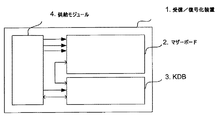
図1は、視聴覚プログラムを受信する装置1の全体的なアーキテクチャを表す。装置1は、マザーボード2及びモジュールKDBのための供給ラインを提供する供給モジュール4を有する。KDB(キー及びディスプレイ・ボード)(Key and Display Board)モジュールは常に供給モジュール4によって給電され、供給モジュール4を制御することによってスタンバイモードを出るよう装置1の起動を管理する。スタンバイモードにおいて、電圧をマザーボード2へ供給する供給ラインの全て又は一部は非作動にされる。これは、スタンバイモードでの大きなエネルギ節約を可能にする。マザーボード2は、装置1のメイン制御ユニットを有し、KDB3は、表示機能に必要な要素、キーボード、及びリモートコントロール用のデータ受信機を有する。マザーボード2がスタンバイモードにある場合に、その制御ユニットはもはや、KDBモジュール3に配置された表示コントローラのメモリに書き込むことができない。その場合に、本発明を構成する方法は、リモートコントロールによって発せられたデータフレームの受信の間、関連するピクトグラムのフリッカ(又は明滅)を引き起こすために使用される。
FIG. 1 represents the overall architecture of a
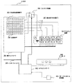
図2は、本発明の実施形態に従う、図1において使用され且つ表されたKDBモジュール3を表す。KDB3は、ディスプレイ装置301と、キーボード302と、赤外線リモートコントロール受信機303と、表示コントローラ304と、マイクロコントローラ305とを有する。マイクロコントローラ305は、表示コントローラ304と共に、受信機デコーダ装置がスタンバイモードにある場合且つマザーボードのモジュールの全て又は一部が給電されない場合に、ディスプレイ、キーボード及びリモートコントロールの管理に必要な動作の主たる部分を確保する。
FIG. 2 represents the
マザーボードの制御ユニットとのやり取りは、インターフェースバス306を用いて行われる。 Communication with the control unit of the motherboard is performed using the interface bus 306.
表示コントローラ304は、ディスプレイ装置301の表示素子と夫々関連する記憶素子308と、付加的な記憶素子309とを有する。スイッチング回路310は、マイクロコントローラ305によって制御され、付加的な記憶素子309が、通常は他の記憶素子と関連付けられている表示素子と関連付けられることを可能にする。 The display controller 304 has a storage element 308 associated with each display element of the display device 301 and an additional storage element 309. The switching circuit 310 is controlled by the microcontroller 305 to allow additional storage elements 309 to be associated with display elements that are normally associated with other storage elements.
ディスプレイ装置301の表示素子における表示は、表示素子の共通ピン307を作動させることができる表示コントローラ304によって順次行われる。 The display on the display element of the display device 301 is sequentially performed by a display controller 304 that can operate the common pin 307 of the display element.
スタンバイモードにおける設定のための要求がマザーボードの制御ユニットによって検出される場合に、制御ユニットは、表示コントローラ304の記憶素子への書込を行う。書込は、インターフェースバス306を用いて行われる。次いで、制御ユニットは、スタンバイモードにおける表示(表示素子と関連する記憶素子)に対応するコンテンツ及び付加的な記憶素子309のコンテンツを書き込む。 When a request for setting in the standby mode is detected by the control unit of the motherboard, the control unit writes to the storage element of the display controller 304. Writing is performed using the interface bus 306. The control unit then writes the content corresponding to the display in the standby mode (the storage element associated with the display element) and the content of the additional storage element 309.
リモートコントロール受信機303による装置リモートコントールによって発せられたデータフレームの受信時に、受信されたデータは、処理のためにマイクロコントローラ305へ送信される。マイクロコントローラ305は、データフレームを検出及び処理し、スイッチング回路310を制御して、リモートコントロールからのデータの受信を表すピクトグラムを有する表示素子が、関連する記憶素子(308)のコンテンツと付加的な記憶素子(309)のコンテンツとに交互に関連付けられるようにする。表示素子レベルで、それはまさに、あたかも、関連する記憶素子のコンテンツが変更されたかのようである。しかし、これは、通常表示素子に関連付けられている記憶素子とは異なるコンテンツを予め有する他の記憶素子を切り替えることによって関連付けることを伴う。 Upon receipt of a data frame issued by device remote control by the remote control receiver 303, the received data is transmitted to the microcontroller 305 for processing. The microcontroller 305 detects and processes the data frame and controls the switching circuit 310 so that the display element having a pictogram representing the receipt of data from the remote control is additionally connected with the contents of the associated storage element (308). The contents are alternately associated with the contents of the storage element (309). At the display element level, it is as if the content of the associated storage element has changed. However, this entails associating by switching other memory elements that already have different content from the memory elements normally associated with the display elements.
表示素子のピクトグラムの制御ライン、従って、表示は、このようにして変更される。 The control line of the pictogram of the display element and thus the display is changed in this way.
実際に、リモートコントロールからのデータフレームの受信を示すピクトグラムを有する表示素子とこのようにして関連付けられ得る2つの記憶素子308及び309が、一方がピクトグラムの作動に、他方がその非作動に対応するコンテンツを予め有している場合に、交互のスイッチングはピクトグラムのフリッカを生じさせる。スタンバイモードにおいて、スタンバイモードの表示のためのピクトグラムの作動に対応する2進要素は、(表示素子及び付加的な記憶素子と関連付けられる)2つの記憶素子において1(作動状態)に設定される。 In fact, two storage elements 308 and 309, which can be associated in this way with a display element having a pictogram indicating the reception of a data frame from a remote control, one corresponds to the operation of the pictogram and the other corresponds to its inactivation. Alternating switching causes pictogram flicker when pre-content. In the standby mode, the binary element corresponding to the operation of the pictogram for displaying the standby mode is set to 1 (active state) in the two storage elements (associated with the display element and the additional storage element).
このように、表示コントローラ304の記憶素子308及び309が装置のスタンバイモードへの切替の前に必要な論理情報を予め有しているという条件で、ピクトグラムの明滅を引き起こすようディスプレイ装置301の表示を変更することが可能である。スタンバイモードは、装置マザーボードの制御ユニットがメモリにアクセスできないようにする。スイッチング回路310は、本発明の実施形態に従って、関連する表示素子の共通ピンが接続又は切断されることを可能にする電子スイッチを有する。スイッチング回路310は、KDBのマイクロコントローラ305の出力ポートへ接続される信号によって制御される。マイクロコントローラ305によって実行されるソフトウェアは、リモートコントロール303の受信機からの信号検出時にスイッチング回路310を制御し、受信機303はマイクロコントローラ305の入力ポートへ接続されている。 As described above, the display device 301 is displayed so as to cause the pictogram to blink, on the condition that the storage elements 308 and 309 of the display controller 304 have logical information necessary before switching the device to the standby mode. It is possible to change. The standby mode prevents the control unit of the device motherboard from accessing the memory. The switching circuit 310 has an electronic switch that allows the common pin of the associated display element to be connected or disconnected in accordance with an embodiment of the present invention. The switching circuit 310 is controlled by a signal connected to the output port of the KDB microcontroller 305. The software executed by the microcontroller 305 controls the switching circuit 310 when a signal from the receiver of the remote control 303 is detected, and the receiver 303 is connected to the input port of the microcontroller 305.
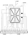
図3は、図2において表されたディスプレイ装置において使用される表示素子30を示す。表示素子30は、独立して作動又は非作動とされ得るピクトグラム31の組を有する。作動中のピクトグラムは装置のユーザに可視的であり、一方、非作動のピクトグラムは可視的でない。実施形態に従って、ピクトグラム31は、関連する記憶素子の対応する2進要素(ビット)が1に設定される場合に、作動し可視的である。逆に、記憶素子が0に設定される場合に、ピクトグラム31は非作動とされ、装置のユーザに不可視である。 FIG. 3 shows a display element 30 used in the display device represented in FIG. The display element 30 has a set of pictograms 31 that can be activated or deactivated independently. The active pictogram is visible to the user of the device, while the inactive pictogram is not visible. According to an embodiment, the pictogram 31 is activated and visible when the corresponding binary element (bit) of the associated storage element is set to 1. Conversely, when the storage element is set to 0, the pictogram 31 is deactivated and is invisible to the user of the device.
ピクトグラム31の作動は表示コントローラによって行われ、供給電圧に接続される共通ピンの原理に従って動作する。次いで、夫々のピクトグラム31は、表示素子30の特定のピンと関連付けられる。作動ピン(及び関連する2進要素)の論理状態は、ピクトグラム31の作動状態及び可視性を定義する。共通ピンによるこのような制御は広く使用されており、電子回路に必要なピン及び制御の数が制限されることを可能にする。 The operation of the pictogram 31 is performed by a display controller and operates according to the principle of a common pin connected to the supply voltage. Each pictogram 31 is then associated with a particular pin of the display element 30. The logic state of the actuation pin (and associated binary element) defines the actuation state and visibility of the pictogram 31. Such control with a common pin is widely used, allowing the number of pins and controls required in an electronic circuit to be limited.
装置301のようにディスプレイ装置が複数の表示素子を使用する場合に、素子の制御は多重化される。素子は多重化周波数により順次制御され、人間の網膜残像によりユーザに対し順次不可視となる。このシステムは、エネルギ、とりわけ、電子回路のための多数のピン及び相互接続が節約されることを可能にする。表示素子の夫々の制御の間、表示コントローラは、対応する記憶素子の内容を作動ピンに設定する。 When the display device uses a plurality of display elements such as the device 301, the control of the elements is multiplexed. The elements are sequentially controlled by the multiplexing frequency, and become invisible to the user by human retinal afterimage. This system allows energy, in particular, a large number of pins and interconnections for electronic circuits to be saved. During each control of the display element, the display controller sets the contents of the corresponding storage element to the operating pin.
図4は、図3において記載されるものと同じ表示素子40を表し、ピクトグラムと作動ピンとの間の相互接続を示し、使用される接続モードをこのようにして表す。表示コントローラの記憶素子のビット位置は、対応するピンの電気的な状態を引き起こし、関連するピクトグラムを可視的とする。共通ピン41及びピクトグラム作動ピン42は区別される。作動ピンの状態は、表示素子に関連する表示素子の記憶素子の2進要素(ビット)の状態に依存する。 FIG. 4 represents the same display element 40 as described in FIG. 3, shows the interconnection between the pictogram and the actuation pin and thus represents the connection mode used. The bit position of the storage element of the display controller causes an electrical state of the corresponding pin, making the associated pictogram visible. The common pin 41 and the pictogram operating pin 42 are distinguished. The state of the actuation pin depends on the state of the binary element (bit) of the storage element of the display element associated with the display element.
実施形態に従って、記憶素子44は、B15からB0を特定する16個の2進要素45を有する。 According to the embodiment, the storage element 44 has 16 binary elements 45 that identify B15 to B0.
表示素子は巧みにスイッチング回路の制御によって他の記憶素子と交互に関連付けられるので、表示コントローラの記憶素子は夫々の表示素子に対応し、リモートコントロールからのデータフレームの受信を示すピクトグラムを除いて2進要素は夫々のピクトグラムに対応する。 Since the display elements are cleverly associated with other storage elements by control of the switching circuit, the storage elements of the display controller correspond to the respective display elements, except for the pictogram indicating the reception of the data frame from the remote control. A hex element corresponds to each pictogram.
図5は、スタンバイモードの起動を表すピクトグラム51と、リモートコントロールのフレームの受信を表すピクトグラム52とを有する表示素子50を表す。この表示素子50は、共通ピンに加えて、2つのピクトグラムの夫々の作動に夫々対応する2つのピンを有する。まさに、英数字が作動中のピクトグラムの組み合わせに従って表示されることを可能にする一般的な表示素子30及び40と同じように、表示素子50のピクトグラム作動ピンの論理状態は、表示コントローラの関連する記憶素子の状態に対応する。 FIG. 5 shows a display element 50 having a pictogram 51 representing activation of the standby mode and a pictogram 52 representing reception of a remote control frame. The display element 50 has two pins corresponding to respective operations of the two pictograms in addition to the common pins. Just as with the typical display elements 30 and 40 that allow alphanumeric characters to be displayed according to the active pictogram combination, the logic state of the pictogram activation pin of the display element 50 is related to the display controller. This corresponds to the state of the storage element.
この表示素子に関連する記憶素子の2進要素は、スタンバイモード表示ピクトグラム51に対応し、記憶素子の他の2進要素は、リモートコントロールによって発せられたデータフレームの受信を表すピクトグラム52に対応する。 The binary element of the storage element associated with this display element corresponds to the standby mode display pictogram 51 and the other binary element of the storage element corresponds to the pictogram 52 representing the reception of the data frame emitted by the remote control. .
図6は、内容“1011001000001001”を表示素子に関連する記憶素子に書き込むことによる表示素子上の数字“3”の表示を表す。 FIG. 6 represents the display of the number “3” on the display element by writing the content “1011001000001001” to the storage element associated with the display element.
図7は、関連する記憶素子及び関連する記憶素子の2進要素とピクトグラムとの間の対応を示すことによって図3の表示素子を表す。 7 represents the display element of FIG. 3 by showing the correspondence between the associated storage element and the binary element of the associated storage element and the pictogram.
この場合において、表示素子は2つのピクトグラムしか有さない。その場合に、記憶素子の2つの2進要素(すなわち、ビット)のみがピクトグラムに関連付けられる。 In this case, the display element has only two pictograms. In that case, only two binary elements (ie, bits) of the storage element are associated with the pictogram.
図8は、方法を表す機能図である。 FIG. 8 is a functional diagram showing the method.
ステップS1は、方法の開始ステップを表す。デコーダは通常の動作状態にあり、特に、使用各プログラムを受信し復号化し、あるいは、このモードにおいて利用可能な何らかの他の機能を確かにすることができる。 Step S1 represents the starting step of the method. The decoder is in a normal operating state, in particular it can receive and decode each program used, or ensure some other function available in this mode.
ステップS2は、スタンバイモードへの切替のための要求の検出に対応する。この検出は、リモートコントロールからの、スタンバイモードへの切替に対応するコードを含むデータフレームの受信(その場合に、ユーザは装置をスタンバイモードに設定する。)に続いて起こることができるが、例えば、所定の期間の間装置機能の作動がない場合にプログラム又は自動化されてよい。実施形態に従って、その時から、スタンバイモードへの切替の前に表示コントローラのメモリへの起こり得る上書きを回避するために、スタンバイモードにおける表示に有用な情報のみがメモリに書き込まれ得る。スタンバイモードへの実際の切替は、表示コントローラのメモリへのアクセスを不可能にする。 Step S2 corresponds to detection of a request for switching to the standby mode. This detection can occur following reception of a data frame from the remote control that includes a code corresponding to switching to standby mode (in which case the user sets the device to standby mode), for example May be programmed or automated when the device function is not activated for a predetermined period of time. In accordance with an embodiment, from then on, only information useful for display in standby mode can be written to the memory to avoid possible overwriting to the memory of the display controller before switching to standby mode. The actual switch to standby mode makes it impossible to access the display controller's memory.
ステップS3は、スタンバイモードの間に表示されるコンテンツ及び付加的な記憶素子のコンテンツの表示コントローラのメモリへの書込に対応する。それらのコンテンツは、既に他の記憶素子と関連付けられた表示素子上で、スイッチング回路を用いることによってスタンバイモードにおいて表示され得る。 Step S3 corresponds to writing the content displayed during the standby mode and the content of the additional storage elements to the memory of the display controller. Those contents can be displayed in standby mode by using switching circuits on display elements already associated with other storage elements.
ステップS4は、デコーダのスタンバイモードへの切替に対応する。マザーボードの全て又は一部は非作動にされ、デコーダの主制御ユニットは非作動にされ、もはや、KDB表示コントローラのメモリへの書込モードにおけるアクセスを有することを可能にしない。 Step S4 corresponds to switching of the decoder to the standby mode. All or part of the motherboard is deactivated and the main control unit of the decoder is deactivated, which no longer makes it possible to have access in write mode to the memory of the KDB display controller.
ステップS5で、マザーボードはスタンバイモードにあるが、KDBは作動中のままであり、イベントの発生を検知する。このように、そのリモートコントロール受信機を用いて、KDBは、特に、リモートコントロールによって発せられたデータフレームの受信を検出することができる。 In step S5, the motherboard is in standby mode, but KDB remains active and detects the occurrence of an event. In this way, using the remote control receiver, the KDB can particularly detect the reception of data frames emitted by the remote control.
ステップS6で、リモートコントロールによって発せられたデータフレームの検出に続いて、リモートコントロール受信機からの信号が接続されるKDBマイクロコントローラは、所定の期間にスイッチング回路を作動させる。次いで、スイッチング回路は、2つの記憶素子のコンテンツを同じ表示素子上で交互に表示するよう表示モジュール制御信号を交互に切り替える。次いで、表示素子は、スタンバイモードへの設定の前に予めロードされたコンテンツを表示する。コンテンツは、リモートコントロールから発せられたデータの受信を象徴するピクトグラムの明滅に対応するように、予め定義されている。スイッチング回路の作動存続期間が経過した場合、処理はステップS4へ戻り、表示素子上の表示により報告されるであろうイベントを待つ。リモートコントロールによって発せられたデータが、デコーダがスタンバイモードを出るべきことをKDBマイクロコントローラに示す場合において、KDBは、通常の動作モードを再開させるよう供給モジュール及びマザーボードを制御する。次いで、処理は最初のステップS1に戻る。 In step S6, following the detection of the data frame emitted by the remote control, the KDB microcontroller to which the signal from the remote control receiver is connected activates the switching circuit for a predetermined period. Next, the switching circuit alternately switches the display module control signals so that the contents of the two storage elements are alternately displayed on the same display element. Next, the display element displays the preloaded content before setting to the standby mode. The content is predefined to correspond to the blinking of the pictogram symbolizing the reception of data originating from the remote control. If the operational lifetime of the switching circuit has elapsed, the process returns to step S4 to wait for an event that will be reported by a display on the display element. In the case where the data emitted by the remote control indicates to the KDB microcontroller that the decoder should exit standby mode, the KDB controls the supply module and the motherboard to resume normal operation mode. Next, the process returns to the first step S1.
実施形態に従って、スイッチング回路は、フリッカ又は明滅効果によらずにピクトグラムをオン又はオフするよう静的に制御されてよい。 According to an embodiment, the switching circuit may be statically controlled to turn the pictogram on or off without flicker or blinking effects.
他の実施形態に従って、検出されるイベントは、リモートコントロールとは無関係であって、現在の時間とプログラムされた時間との間の一致の検出によって起こってよく、KDBはシステムクロック機能を確保する。次いで、デコーダは、例えば、接続される周辺機器で受信されるフローの記録のような機能を有効にし、この記録機能の作動をピクトグラムの出現により示すことができる。なお、このような機能の作動は、たとえスタンバイモードにあってもデコーダ・マザーボードの素子が有効なままである場合にのみ、可能である。実際に、デコーダの通常動作の低下モードに対応し、一部の機能が作動し、一方、他の機能がエネルギ節約のために非作動にされることを可能にする様々なタイプのスタンバイモードが存在する。従って、本発明の他の実施形態に従って、現在の時間が視聴覚プログラムの記録の予約時間に対応することを検出し、デコーダの主制御ユニットが表示コントローラのメモリに書き込むことができない場合に、たとえ通常の動作モードにないとしてもこの記録を実施し、スイッチング回路を作動させることで関連するピクトグラムを表示することによって記録を示すことが可能である。ピクトグラムは、表示コントローラの記憶素子に予めロードされており、作動回路は、表示素子にこの記憶素子のコンテンツを表示するよう制御される。 According to other embodiments, the detected event is independent of the remote control and may occur by detecting a match between the current time and the programmed time, and KDB ensures system clock functionality. The decoder can then enable functions such as recording the flow received at the connected peripheral device, and the operation of this recording function can be indicated by the appearance of a pictogram. Such a function can be activated only when the elements of the decoder / motherboard remain valid even in the standby mode. In fact, there are various types of standby modes that correspond to the reduced mode of normal operation of the decoder and allow some functions to be activated while others can be deactivated to save energy. Exists. Therefore, in accordance with another embodiment of the present invention, even if it is detected that the current time corresponds to the scheduled recording time of the audiovisual program and the main control unit of the decoder cannot write to the memory of the display controller, it is Even if you are not in this mode of operation, you can perform this recording and activate the switching circuit to show the recording by displaying the associated pictogram. The pictogram is pre-loaded into the storage element of the display controller and the actuation circuit is controlled to display the contents of this storage element on the display element.
また、本発明は、スタンバイモードにおいて設定され且つ制御ユニットが表示コントローラのメモリへのアクセスを有することができないように構成され、ユーザに可視的なプログラムがイベントを報告するために変更されることを可能にするようなあらゆる電子機器に関する。関連する電子機器は、一例として、TVセット、プログラム再生機、放送データの受信機、ゲーム機、スクリーンである。
上記の実施形態に加えて、以下の付記を開示する。
(付記1)
少なくとも1つのピクトグラムを有する少なくとも1つの表示素子と、該少なくとも1つの表示素子に関連する少なくとも1つの記憶素子を有する第1のメモリ、及び少なくとも1つの記憶素子を有する第2のメモリを有する1つの表示コントローラと、1つのスイッチング回路とを有する電子機器におけるディスプレイ装置の制御方法であって、
コンテンツを前記第1のメモリの少なくとも1つの記憶素子と前記第2のメモリの少なくとも1つの記憶素子とに書き込むステップと、
前記電子機器のスタンバイモードを設定するステップと、
前記スイッチング回路に接続されるマイクロコントローラによって、表示によって示されるイベントを検出するステップと、
前記スタンバイモードの設定後且つ前記イベントの検出前に、前記第1のメモリ及び前記第2のメモリへのアクセスをブロックするステップと、
前記少なくとも1つの表示素子の表示を前記第1のメモリの少なくとも1つの記憶素子と前記第2のメモリの少なくとも1つの記憶素子とに交互に関連付けることによって前記少なくとも1つの表示素子の表示を変更するよう前記スイッチング回路を制御するステップと
を有することを特徴とする電子機器におけるディスプレイ装置の制御方法。
(付記2)
コンテンツを前記第1のメモリの少なくとも1つの記憶素子と前記第2のメモリの少なくとも1つの記憶素子とに書き込む前記ステップは、制御ユニットがスタンバイモードへの切替のための信号を検出することによってトリガされる、
ことを特徴とする付記1に記載の電子機器におけるディスプレイ装置の制御方法。
(付記3)
前記検出されるイベントは、前記電子機器のリモートコントロールによって発せられるデータフレームの受信に対応する、
ことを特徴とする付記1又は2に記載の電子機器におけるディスプレイ装置の制御方法。
(付記4)
イベントを検出する前記ステップは、前記スイッチング回路に接続されるマイクロコントローラが前記電子機器のキーボードのキーの押下に続く信号の変化を検出することに対応する、
ことを特徴とする付記1又は2に記載の電子機器におけるディスプレイ装置の制御方法。
(付記5)
イベントを検出する前記ステップは、前記スイッチング回路に接続されるマイクロコントローラによって現在の時間と前記電子機器の機能の作動を生じさせるプログラムされた時間とが一致することが検出されることに対応する、
ことを特徴とする付記1又は2に記載の電子機器におけるディスプレイ装置の制御方法。
(付記6)
少なくとも1つのピクトグラムを有する少なくとも1つの表示素子と、該少なくとも1つの表示素子に関連する少なくとも1つの記憶素子を有する第1のメモリを有する表示コントローラと、スイッチング手段とを有する電子機器におけるディスプレイ装置であって、
前記表示コントローラは第2のメモリを更に有し、
当該ディスプレイ装置は、前記電子機器のスタンバイモード設定によってトリガされるよう構成された、前記第1のメモリ及び前記第2のメモリへのアクセスをブロックする手段を有し、
前記スイッチング手段は、前記少なくとも1つの表示素子を前記第2のメモリと前記第1のメモリの少なくとも1つの記憶素子とに交互に関連付けるよう構成され、イベントの検出によってトリガされ得る、
ことを特徴とするディスプレイ装置。
(付記7)
前記電子機器は、視聴覚プログラムの受信機である、
ことを特徴とする付記6に記載のディスプレイ装置。
(付記8)
前記少なくとも1つのピクトグラムは、前記電子機器のリモートコントロールによって発せられるコマンドの受信を示す、
ことを特徴とする付記6又は7に記載のディスプレイ装置。
The present invention also provides that the control unit configured in standby mode and configured so that the control unit cannot have access to the memory of the display controller is modified to report the event to the user. It relates to any electronic device that makes it possible. Related electronic devices are, for example, a TV set, a program player, a broadcast data receiver, a game machine, and a screen.
In addition to the above embodiment, the following supplementary notes are disclosed.
(Appendix 1)
One having at least one display element having at least one pictogram; a first memory having at least one storage element associated with the at least one display element; and a second memory having at least one storage element. A control method for a display device in an electronic apparatus having a display controller and one switching circuit,
Writing content to at least one storage element of the first memory and to at least one storage element of the second memory;
Setting a standby mode of the electronic device;
Detecting an event indicated by a display by a microcontroller connected to the switching circuit;
Blocking access to the first memory and the second memory after setting the standby mode and before detecting the event;
Altering the display of the at least one display element by alternately associating the display of the at least one display element with at least one storage element of the first memory and at least one storage element of the second memory; Controlling the switching circuit and
A method for controlling a display device in an electronic apparatus.
(Appendix 2)
The step of writing content into at least one storage element of the first memory and at least one storage element of the second memory is triggered by a control unit detecting a signal for switching to standby mode. To be
The control method of the display apparatus in the electronic device of
(Appendix 3)
The detected event corresponds to reception of a data frame emitted by a remote control of the electronic device;
The control method of the display apparatus in the electronic device of
(Appendix 4)
The step of detecting an event corresponds to detecting a change in a signal following a press of a key on a keyboard of the electronic device by a microcontroller connected to the switching circuit;
The control method of the display apparatus in the electronic device of
(Appendix 5)
The step of detecting an event corresponds to detecting by a microcontroller connected to the switching circuit that a current time and a programmed time causing the activation of the function of the electronic device coincide;
The control method of the display apparatus in the electronic device of
(Appendix 6)
A display device in an electronic apparatus, comprising: a display controller having at least one display element having at least one pictogram; a first memory having at least one storage element associated with the at least one display element; and switching means. There,
The display controller further comprises a second memory;
The display device includes means for blocking access to the first memory and the second memory configured to be triggered by a standby mode setting of the electronic device;
The switching means is configured to alternately associate the at least one display element with the second memory and at least one storage element of the first memory, and may be triggered by detection of an event;
A display device.
(Appendix 7)
The electronic device is a receiver of an audiovisual program;
The display device according to appendix 6, wherein:
(Appendix 8)
The at least one pictogram indicates receipt of a command issued by a remote control of the electronic device;
The display device according to appendix 6 or 7, characterized by the above.
1 受信/復号化装置
2 マザーボード
3 KDBモジュール
4 供給モジュール
30,40,50 表示素子
31,43,51,52 ピクトグラム
42 ピクトグラム作動ピン
45 2進要素
301 ディスプレイ装置
302 キーボード
303 赤外線リモートコントロール受信機
304 表示コントローラ
305 マイクロコントローラ
306 インターフェースバス
41,307 共通ピン
44,308 記憶素子
309 付加的な記憶素子
310 スイッチング回路
DESCRIPTION OF
Claims (8)
コンテンツを前記第1のメモリの少なくとも1つの記憶素子と前記第2のメモリの少なくとも1つの記憶素子とに書き込み、
前記電子機器をスタンバイモードに設定し、前記第1のメモリ及び前記第2のメモリへの書込アクセスをブロックし、
前記スイッチング回路に接続されるマイクロコントローラによって、表示によって示されるイベントを検出し、
前記少なくとも1つの表示素子を前記第1のメモリの少なくとも1つの記憶素子と前記第2のメモリの少なくとも1つの記憶素子とに交互に関連付けることによって前記少なくとも1つの表示素子の表示を変更するよう前記スイッチング回路を制御する
ことを有する、電子機器におけるディスプレイ装置の制御方法。 One having at least one display element having at least one pictogram; a first memory having at least one storage element associated with the at least one display element; and a second memory having at least one storage element. A control method for a display device in an electronic apparatus having a display controller and one switching circuit,
Write the content into at least one storage element of the second memory and at least one storage element of said first memory,
Setting the electronic device to a standby mode , blocking write access to the first memory and the second memory ;
The microcontroller connected to the switching circuit detects the event indicated by the display ;
To change the display of the at least one display device by associating the alternating at least one display element on the at least one storage element of said first of said second memory and at least one storage element of the memory that controls the switching circuit
A method for controlling a display device in an electronic apparatus.
請求項1に記載の電子機器におけるディスプレイ装置の制御方法。 Writing the content into at least one storage element of at least one of said second memory and storage elements of the first memory is triggered by the control unit detects a signal for switching to standby mode To be
Control method of a display device in an electronic device according to 請 Motomeko 1.
請求項1又は2に記載の電子機器におけるディスプレイ装置の制御方法。 The detected event corresponds to reception of a data frame emitted by a remote control of the electronic device;
Control method of a display device in an electronic device according to 請 Motomeko 1 or 2.
請求項1又は2に記載の電子機器におけるディスプレイ装置の制御方法。 Detecting said event includes that the micro-controller coupled to the switching circuit, detecting a change in the subsequent signal to the depression of a key of the keyboard of the electronic device,
Control method of a display device in an electronic device according to 請 Motomeko 1 or 2.
請求項1又は2に記載の電子機器におけるディスプレイ装置の制御方法。 Detecting said event includes that the micro-controller coupled to the switching circuit, for detecting coincidence between the current time and the programmed time causes activation of functions of the electronic device,
Control method of a display device in an electronic device according to 請 Motomeko 1 or 2.
前記表示コントローラは第2のメモリを更に有し、
当該ディスプレイ装置は、前記電子機器のスタンバイモード設定によってトリガされるよう構成された、前記第1のメモリ及び前記第2のメモリへの書込アクセスをブロックする手段を有し、
前記スイッチング手段は、前記少なくとも1つの表示素子を前記第2のメモリと前記第1のメモリの少なくとも1つの記憶素子とに交互に関連付けるよう構成され、イベントの検出によってトリガされ得る、
ディスプレイ装置。 A display device in an electronic apparatus, comprising: a display controller having at least one display element having at least one pictogram; a first memory having at least one storage element associated with the at least one display element; and switching means. There,
The display controller further comprises a second memory;
The display device includes means for blocking write access to the first memory and the second memory configured to be triggered by a standby mode setting of the electronic device;
The switching means is configured to alternately associate the at least one display element with the second memory and at least one storage element of the first memory, and may be triggered by detection of an event;
De Isupurei apparatus.
請求項6に記載のディスプレイ装置。 The electronic device is a receiver of an audiovisual program;
The display device according to claim 6.
ことを特徴とする請求項6又は7に記載のディスプレイ装置。 One pictogram even without least indicates the reception of a command emitted by the remote control of the electronic device,
The display device according to claim 6, wherein the display device is a display device.
Applications Claiming Priority (2)
| Application Number | Priority Date | Filing Date | Title |
|---|---|---|---|
| FR1157844 | 2011-09-05 | ||
| FR1157844 | 2011-09-05 |
Publications (3)
| Publication Number | Publication Date |
|---|---|
| JP2013054353A JP2013054353A (en) | 2013-03-21 |
| JP2013054353A5 JP2013054353A5 (en) | 2015-10-01 |
| JP5978068B2 true JP5978068B2 (en) | 2016-08-24 |
Family
ID=46724288
Family Applications (1)
| Application Number | Title | Priority Date | Filing Date |
|---|---|---|---|
| JP2012188540A Active JP5978068B2 (en) | 2011-09-05 | 2012-08-29 | Display device in electronic apparatus and control method thereof |
Country Status (5)
| Country | Link |
|---|---|
| US (1) | US9158365B2 (en) |
| EP (1) | EP2565749B1 (en) |
| JP (1) | JP5978068B2 (en) |
| KR (1) | KR101926617B1 (en) |
| CN (1) | CN102984570B (en) |
Families Citing this family (9)
| Publication number | Priority date | Publication date | Assignee | Title |
|---|---|---|---|---|
| US9324220B2 (en) * | 2012-08-21 | 2016-04-26 | Southern Imperial, Inc. | Theft detection device and method for controlling same |
| KR102349861B1 (en) * | 2015-09-16 | 2022-01-12 | 삼성전자주식회사 | Display apparatus and method for controlling a display of display apparatus |
| KR20170073257A (en) * | 2015-12-18 | 2017-06-28 | 삼성전자주식회사 | Display apparatus and method for controlling a display apparatus |
| CN106409220B (en) * | 2016-09-29 | 2019-01-29 | 深圳创维-Rgb电子有限公司 | A kind of OLED drive electric power unit and OLED TV |
| US10885753B2 (en) | 2018-03-21 | 2021-01-05 | Fasteners For Retail, Inc. | Anti-theft device with remote alarm feature |
| CN111385653B (en) * | 2018-12-29 | 2021-11-09 | 深圳Tcl新技术有限公司 | Processing method and device based on standby process, smart television and storage medium |
| JP7206953B2 (en) * | 2019-01-28 | 2023-01-18 | セイコーエプソン株式会社 | Liquid crystal devices, liquid crystal drivers, electronic devices and moving bodies |
| US11087601B1 (en) | 2020-04-02 | 2021-08-10 | Fasteners For Retail, Inc | Anti-theft device with cable attachment |
| USD956607S1 (en) | 2020-04-16 | 2022-07-05 | Fasteners For Retail, Inc. | Security tag holder |
Family Cites Families (16)
| Publication number | Priority date | Publication date | Assignee | Title |
|---|---|---|---|---|
| US5887176A (en) * | 1996-06-28 | 1999-03-23 | Randtec, Inc. | Method and system for remote monitoring and tracking of inventory |
| JP3798476B2 (en) * | 1996-08-30 | 2006-07-19 | 株式会社東芝 | Computer system and cache memory power-down control method in the system |
| JP4095158B2 (en) * | 1998-04-28 | 2008-06-04 | イーストマン コダック カンパニー | Electronic still camera |
| CN1599924A (en) * | 2001-12-05 | 2005-03-23 | 皇家飞利浦电子股份有限公司 | Method for driving a liquid crystal display device in normal and standby mode |
| US7437575B2 (en) * | 2003-05-29 | 2008-10-14 | Dell Products L.P. | Low power mode for device power management |
| WO2005073904A1 (en) * | 2004-01-30 | 2005-08-11 | Semiconductor Energy Laboratory Co., Ltd. | Semiconductor device |
| KR20060033329A (en) | 2004-10-14 | 2006-04-19 | 엘지전자 주식회사 | Led control device for mobile appliance |
| US8593470B2 (en) * | 2005-02-24 | 2013-11-26 | Ati Technologies Ulc | Dynamic memory clock switching circuit and method for adjusting power consumption |
| CN1870845A (en) | 2005-05-24 | 2006-11-29 | 乐金电子(昆山)电脑有限公司 | LED control device on portable equipment |
| JP2008145893A (en) * | 2006-12-12 | 2008-06-26 | Sharp Corp | Display memory, display device and portable electronic information device |
| US8181042B2 (en) * | 2007-02-12 | 2012-05-15 | Atmel Corporation | Low power mode data preservation in secure ICs |
| US20080235527A1 (en) * | 2007-03-19 | 2008-09-25 | Winbond Electronics Corporation | Operation of computer display using auxiliary display controller |
| US8555326B2 (en) * | 2008-05-13 | 2013-10-08 | Sony Corporation | Display device detection of and response to an idle mode of a remote sender device |
| CN101727801B (en) * | 2008-10-31 | 2012-04-11 | 扬智科技股份有限公司 | Integrated circuit for controlling operation of displaying module and first circuit module with shared connecting pin |
| US20110084979A1 (en) * | 2009-10-09 | 2011-04-14 | Firstpaper Llc | Integrated electronic paper display controller |
| US8443221B2 (en) * | 2011-03-04 | 2013-05-14 | Sandisk Technologies Inc. | Methods, systems, and computer readable media for advanced power management for serial advanced technology attachment (SATA)-based storage devices |
-
2012
- 2012-08-27 EP EP12181892.6A patent/EP2565749B1/en active Active
- 2012-08-29 JP JP2012188540A patent/JP5978068B2/en active Active
- 2012-09-04 US US13/602,361 patent/US9158365B2/en active Active
- 2012-09-04 KR KR1020120097727A patent/KR101926617B1/en active IP Right Grant
- 2012-09-05 CN CN201210325402.XA patent/CN102984570B/en active Active
Also Published As
| Publication number | Publication date |
|---|---|
| EP2565749A1 (en) | 2013-03-06 |
| US20130057524A1 (en) | 2013-03-07 |
| JP2013054353A (en) | 2013-03-21 |
| KR20130026397A (en) | 2013-03-13 |
| EP2565749B1 (en) | 2014-04-30 |
| KR101926617B1 (en) | 2019-03-07 |
| CN102984570B (en) | 2017-09-05 |
| US9158365B2 (en) | 2015-10-13 |
| CN102984570A (en) | 2013-03-20 |
Similar Documents
| Publication | Publication Date | Title |
|---|---|---|
| JP5978068B2 (en) | Display device in electronic apparatus and control method thereof | |
| US8909960B1 (en) | Power management architecture, method and configuration system | |
| EP1920308B1 (en) | Method and apparatus for supplying power, and display device | |
| US20120133520A1 (en) | Computer chassis system and hard disk status display method thereof | |
| US8405602B2 (en) | Information processing apparatus and method of controlling the same | |
| US8522054B2 (en) | Stand-by mode management method for use in a stand-by mode of a computer system with stand-by mode management module | |
| CN1987732A (en) | One key on-and-off unit for computer and reset device and method | |
| US7447928B2 (en) | Method for booting computer multimedia systems with a hot key standby state | |
| US5864656A (en) | System for automatic fault detection and recovery in a computer system | |
| KR20010027087A (en) | Apparatus and method for power management of computer system | |
| US8769326B2 (en) | Computer system and operation method for changing operation state by capacitive button group | |
| US20070192579A1 (en) | Computer and control method thereof | |
| US20100110021A1 (en) | Electronic device equipped with interactive display screen and processing method for interactive displaying | |
| KR950005225B1 (en) | Data processor | |
| EP3477425A1 (en) | Computer system, client device and display device | |
| US20090276613A1 (en) | Method of sharing basic input output system, and blade server and computer using the same | |
| KR20010086518A (en) | An automatic security code verifying method of a computer system operated by a remote controller | |
| WO2020248870A1 (en) | Backlight control method, driving circuit, and display device | |
| CN102334084B (en) | Method and system to lower power consumption | |
| US20030233591A1 (en) | Power state sub-system and a method of changing the power state of a selected computer system | |
| KR20180037461A (en) | Electronic device and method for controlling thereof | |
| US20110231679A1 (en) | Energy saving device | |
| CN112948297A (en) | Screen control method and device, double-screen terminal equipment and storage medium | |
| CN106775395B (en) | Voice touch screen equipment with single key and method for realizing state switching and identity verification by using key | |
| CN110554731A (en) | Clock synchronization control method, intelligent terminal and storage medium |
Legal Events
| Date | Code | Title | Description |
|---|---|---|---|
| A521 | Request for written amendment filed |
Free format text: JAPANESE INTERMEDIATE CODE: A523 Effective date: 20150814 |
|
| A621 | Written request for application examination |
Free format text: JAPANESE INTERMEDIATE CODE: A621 Effective date: 20150814 |
|
| A977 | Report on retrieval |
Free format text: JAPANESE INTERMEDIATE CODE: A971007 Effective date: 20160531 |
|
| TRDD | Decision of grant or rejection written | ||
| A01 | Written decision to grant a patent or to grant a registration (utility model) |
Free format text: JAPANESE INTERMEDIATE CODE: A01 Effective date: 20160628 |
|
| A61 | First payment of annual fees (during grant procedure) |
Free format text: JAPANESE INTERMEDIATE CODE: A61 Effective date: 20160725 |
|
| R150 | Certificate of patent or registration of utility model |
Ref document number: 5978068 Country of ref document: JP Free format text: JAPANESE INTERMEDIATE CODE: R150 |
|
| S111 | Request for change of ownership or part of ownership |
Free format text: JAPANESE INTERMEDIATE CODE: R313113 |
|
| S531 | Written request for registration of change of domicile |
Free format text: JAPANESE INTERMEDIATE CODE: R313531 |
|
| R371 | Transfer withdrawn |
Free format text: JAPANESE INTERMEDIATE CODE: R371 |
|
| R371 | Transfer withdrawn |
Free format text: JAPANESE INTERMEDIATE CODE: R371 |
|
| R250 | Receipt of annual fees |
Free format text: JAPANESE INTERMEDIATE CODE: R250 |
|
| S531 | Written request for registration of change of domicile |
Free format text: JAPANESE INTERMEDIATE CODE: R313531 |
|
| R350 | Written notification of registration of transfer |
Free format text: JAPANESE INTERMEDIATE CODE: R350 |
|
| S111 | Request for change of ownership or part of ownership |
Free format text: JAPANESE INTERMEDIATE CODE: R313113 |
|
| R350 | Written notification of registration of transfer |
Free format text: JAPANESE INTERMEDIATE CODE: R350 |
|
| R250 | Receipt of annual fees |
Free format text: JAPANESE INTERMEDIATE CODE: R250 |
|
| R250 | Receipt of annual fees |
Free format text: JAPANESE INTERMEDIATE CODE: R250 |
|
| R250 | Receipt of annual fees |
Free format text: JAPANESE INTERMEDIATE CODE: R250 |
|
| R250 | Receipt of annual fees |
Free format text: JAPANESE INTERMEDIATE CODE: R250 |