JP5966009B2 - Stub minimization using a dual set of signal terminals in the assembly without wire bonding to the package substrate - Google Patents
Stub minimization using a dual set of signal terminals in the assembly without wire bonding to the package substrate Download PDFInfo
- Publication number
- JP5966009B2 JP5966009B2 JP2014534602A JP2014534602A JP5966009B2 JP 5966009 B2 JP5966009 B2 JP 5966009B2 JP 2014534602 A JP2014534602 A JP 2014534602A JP 2014534602 A JP2014534602 A JP 2014534602A JP 5966009 B2 JP5966009 B2 JP 5966009B2
- Authority
- JP
- Japan
- Prior art keywords
- grid
- microelectronic
- terminal
- package
- terminals
- Prior art date
- Legal status (The legal status is an assumption and is not a legal conclusion. Google has not performed a legal analysis and makes no representation as to the accuracy of the status listed.)
- Expired - Fee Related
Links
Images


Classifications
-
- H—ELECTRICITY
- H01—ELECTRIC ELEMENTS
- H01L—SEMICONDUCTOR DEVICES NOT COVERED BY CLASS H10
- H01L25/00—Assemblies consisting of a plurality of individual semiconductor or other solid state devices ; Multistep manufacturing processes thereof
- H01L25/03—Assemblies consisting of a plurality of individual semiconductor or other solid state devices ; Multistep manufacturing processes thereof all the devices being of a type provided for in the same subgroup of groups H01L27/00 - H01L33/00, or in a single subclass of H10K, H10N, e.g. assemblies of rectifier diodes
- H01L25/04—Assemblies consisting of a plurality of individual semiconductor or other solid state devices ; Multistep manufacturing processes thereof all the devices being of a type provided for in the same subgroup of groups H01L27/00 - H01L33/00, or in a single subclass of H10K, H10N, e.g. assemblies of rectifier diodes the devices not having separate containers
- H01L25/065—Assemblies consisting of a plurality of individual semiconductor or other solid state devices ; Multistep manufacturing processes thereof all the devices being of a type provided for in the same subgroup of groups H01L27/00 - H01L33/00, or in a single subclass of H10K, H10N, e.g. assemblies of rectifier diodes the devices not having separate containers the devices being of a type provided for in group H01L27/00
- H01L25/0655—Assemblies consisting of a plurality of individual semiconductor or other solid state devices ; Multistep manufacturing processes thereof all the devices being of a type provided for in the same subgroup of groups H01L27/00 - H01L33/00, or in a single subclass of H10K, H10N, e.g. assemblies of rectifier diodes the devices not having separate containers the devices being of a type provided for in group H01L27/00 the devices being arranged next to each other
-
- G—PHYSICS
- G11—INFORMATION STORAGE
- G11C—STATIC STORES
- G11C5/00—Details of stores covered by group G11C11/00
- G11C5/02—Disposition of storage elements, e.g. in the form of a matrix array
- G11C5/04—Supports for storage elements, e.g. memory modules; Mounting or fixing of storage elements on such supports
-
- G—PHYSICS
- G11—INFORMATION STORAGE
- G11C—STATIC STORES
- G11C5/00—Details of stores covered by group G11C11/00
- G11C5/06—Arrangements for interconnecting storage elements electrically, e.g. by wiring
- G11C5/063—Voltage and signal distribution in integrated semi-conductor memory access lines, e.g. word-line, bit-line, cross-over resistance, propagation delay
-
- H—ELECTRICITY
- H01—ELECTRIC ELEMENTS
- H01L—SEMICONDUCTOR DEVICES NOT COVERED BY CLASS H10
- H01L23/00—Details of semiconductor or other solid state devices
- H01L23/12—Mountings, e.g. non-detachable insulating substrates
- H01L23/13—Mountings, e.g. non-detachable insulating substrates characterised by the shape
-
- H—ELECTRICITY
- H01—ELECTRIC ELEMENTS
- H01L—SEMICONDUCTOR DEVICES NOT COVERED BY CLASS H10
- H01L23/00—Details of semiconductor or other solid state devices
- H01L23/48—Arrangements for conducting electric current to or from the solid state body in operation, e.g. leads, terminal arrangements ; Selection of materials therefor
- H01L23/488—Arrangements for conducting electric current to or from the solid state body in operation, e.g. leads, terminal arrangements ; Selection of materials therefor consisting of soldered or bonded constructions
- H01L23/498—Leads, i.e. metallisations or lead-frames on insulating substrates, e.g. chip carriers
- H01L23/49838—Geometry or layout
-
- H—ELECTRICITY
- H01—ELECTRIC ELEMENTS
- H01L—SEMICONDUCTOR DEVICES NOT COVERED BY CLASS H10
- H01L23/00—Details of semiconductor or other solid state devices
- H01L23/48—Arrangements for conducting electric current to or from the solid state body in operation, e.g. leads, terminal arrangements ; Selection of materials therefor
- H01L23/50—Arrangements for conducting electric current to or from the solid state body in operation, e.g. leads, terminal arrangements ; Selection of materials therefor for integrated circuit devices, e.g. power bus, number of leads
-
- H—ELECTRICITY
- H01—ELECTRIC ELEMENTS
- H01L—SEMICONDUCTOR DEVICES NOT COVERED BY CLASS H10
- H01L24/00—Arrangements for connecting or disconnecting semiconductor or solid-state bodies; Methods or apparatus related thereto
- H01L24/01—Means for bonding being attached to, or being formed on, the surface to be connected, e.g. chip-to-package, die-attach, "first-level" interconnects; Manufacturing methods related thereto
- H01L24/18—High density interconnect [HDI] connectors; Manufacturing methods related thereto
- H01L24/19—Manufacturing methods of high density interconnect preforms
-
- H—ELECTRICITY
- H01—ELECTRIC ELEMENTS
- H01L—SEMICONDUCTOR DEVICES NOT COVERED BY CLASS H10
- H01L24/00—Arrangements for connecting or disconnecting semiconductor or solid-state bodies; Methods or apparatus related thereto
- H01L24/01—Means for bonding being attached to, or being formed on, the surface to be connected, e.g. chip-to-package, die-attach, "first-level" interconnects; Manufacturing methods related thereto
- H01L24/18—High density interconnect [HDI] connectors; Manufacturing methods related thereto
- H01L24/20—Structure, shape, material or disposition of high density interconnect preforms
-
- H—ELECTRICITY
- H01—ELECTRIC ELEMENTS
- H01L—SEMICONDUCTOR DEVICES NOT COVERED BY CLASS H10
- H01L24/00—Arrangements for connecting or disconnecting semiconductor or solid-state bodies; Methods or apparatus related thereto
- H01L24/01—Means for bonding being attached to, or being formed on, the surface to be connected, e.g. chip-to-package, die-attach, "first-level" interconnects; Manufacturing methods related thereto
- H01L24/18—High density interconnect [HDI] connectors; Manufacturing methods related thereto
- H01L24/23—Structure, shape, material or disposition of the high density interconnect connectors after the connecting process
- H01L24/24—Structure, shape, material or disposition of the high density interconnect connectors after the connecting process of an individual high density interconnect connector
-
- H—ELECTRICITY
- H01—ELECTRIC ELEMENTS
- H01L—SEMICONDUCTOR DEVICES NOT COVERED BY CLASS H10
- H01L25/00—Assemblies consisting of a plurality of individual semiconductor or other solid state devices ; Multistep manufacturing processes thereof
- H01L25/03—Assemblies consisting of a plurality of individual semiconductor or other solid state devices ; Multistep manufacturing processes thereof all the devices being of a type provided for in the same subgroup of groups H01L27/00 - H01L33/00, or in a single subclass of H10K, H10N, e.g. assemblies of rectifier diodes
- H01L25/04—Assemblies consisting of a plurality of individual semiconductor or other solid state devices ; Multistep manufacturing processes thereof all the devices being of a type provided for in the same subgroup of groups H01L27/00 - H01L33/00, or in a single subclass of H10K, H10N, e.g. assemblies of rectifier diodes the devices not having separate containers
- H01L25/065—Assemblies consisting of a plurality of individual semiconductor or other solid state devices ; Multistep manufacturing processes thereof all the devices being of a type provided for in the same subgroup of groups H01L27/00 - H01L33/00, or in a single subclass of H10K, H10N, e.g. assemblies of rectifier diodes the devices not having separate containers the devices being of a type provided for in group H01L27/00
- H01L25/0652—Assemblies consisting of a plurality of individual semiconductor or other solid state devices ; Multistep manufacturing processes thereof all the devices being of a type provided for in the same subgroup of groups H01L27/00 - H01L33/00, or in a single subclass of H10K, H10N, e.g. assemblies of rectifier diodes the devices not having separate containers the devices being of a type provided for in group H01L27/00 the devices being arranged next and on each other, i.e. mixed assemblies
-
- H—ELECTRICITY
- H01—ELECTRIC ELEMENTS
- H01L—SEMICONDUCTOR DEVICES NOT COVERED BY CLASS H10
- H01L25/00—Assemblies consisting of a plurality of individual semiconductor or other solid state devices ; Multistep manufacturing processes thereof
- H01L25/03—Assemblies consisting of a plurality of individual semiconductor or other solid state devices ; Multistep manufacturing processes thereof all the devices being of a type provided for in the same subgroup of groups H01L27/00 - H01L33/00, or in a single subclass of H10K, H10N, e.g. assemblies of rectifier diodes
- H01L25/04—Assemblies consisting of a plurality of individual semiconductor or other solid state devices ; Multistep manufacturing processes thereof all the devices being of a type provided for in the same subgroup of groups H01L27/00 - H01L33/00, or in a single subclass of H10K, H10N, e.g. assemblies of rectifier diodes the devices not having separate containers
- H01L25/065—Assemblies consisting of a plurality of individual semiconductor or other solid state devices ; Multistep manufacturing processes thereof all the devices being of a type provided for in the same subgroup of groups H01L27/00 - H01L33/00, or in a single subclass of H10K, H10N, e.g. assemblies of rectifier diodes the devices not having separate containers the devices being of a type provided for in group H01L27/00
- H01L25/0657—Stacked arrangements of devices
-
- H—ELECTRICITY
- H01—ELECTRIC ELEMENTS
- H01L—SEMICONDUCTOR DEVICES NOT COVERED BY CLASS H10
- H01L2224/00—Indexing scheme for arrangements for connecting or disconnecting semiconductor or solid-state bodies and methods related thereto as covered by H01L24/00
- H01L2224/01—Means for bonding being attached to, or being formed on, the surface to be connected, e.g. chip-to-package, die-attach, "first-level" interconnects; Manufacturing methods related thereto
- H01L2224/02—Bonding areas; Manufacturing methods related thereto
- H01L2224/023—Redistribution layers [RDL] for bonding areas
- H01L2224/0237—Disposition of the redistribution layers
- H01L2224/02375—Top view
-
- H—ELECTRICITY
- H01—ELECTRIC ELEMENTS
- H01L—SEMICONDUCTOR DEVICES NOT COVERED BY CLASS H10
- H01L2224/00—Indexing scheme for arrangements for connecting or disconnecting semiconductor or solid-state bodies and methods related thereto as covered by H01L24/00
- H01L2224/01—Means for bonding being attached to, or being formed on, the surface to be connected, e.g. chip-to-package, die-attach, "first-level" interconnects; Manufacturing methods related thereto
- H01L2224/02—Bonding areas; Manufacturing methods related thereto
- H01L2224/023—Redistribution layers [RDL] for bonding areas
- H01L2224/0237—Disposition of the redistribution layers
- H01L2224/02379—Fan-out arrangement
-
- H—ELECTRICITY
- H01—ELECTRIC ELEMENTS
- H01L—SEMICONDUCTOR DEVICES NOT COVERED BY CLASS H10
- H01L2224/00—Indexing scheme for arrangements for connecting or disconnecting semiconductor or solid-state bodies and methods related thereto as covered by H01L24/00
- H01L2224/01—Means for bonding being attached to, or being formed on, the surface to be connected, e.g. chip-to-package, die-attach, "first-level" interconnects; Manufacturing methods related thereto
- H01L2224/02—Bonding areas; Manufacturing methods related thereto
- H01L2224/04—Structure, shape, material or disposition of the bonding areas prior to the connecting process
- H01L2224/0401—Bonding areas specifically adapted for bump connectors, e.g. under bump metallisation [UBM]
-
- H—ELECTRICITY
- H01—ELECTRIC ELEMENTS
- H01L—SEMICONDUCTOR DEVICES NOT COVERED BY CLASS H10
- H01L2224/00—Indexing scheme for arrangements for connecting or disconnecting semiconductor or solid-state bodies and methods related thereto as covered by H01L24/00
- H01L2224/01—Means for bonding being attached to, or being formed on, the surface to be connected, e.g. chip-to-package, die-attach, "first-level" interconnects; Manufacturing methods related thereto
- H01L2224/02—Bonding areas; Manufacturing methods related thereto
- H01L2224/04—Structure, shape, material or disposition of the bonding areas prior to the connecting process
- H01L2224/04042—Bonding areas specifically adapted for wire connectors, e.g. wirebond pads
-
- H—ELECTRICITY
- H01—ELECTRIC ELEMENTS
- H01L—SEMICONDUCTOR DEVICES NOT COVERED BY CLASS H10
- H01L2224/00—Indexing scheme for arrangements for connecting or disconnecting semiconductor or solid-state bodies and methods related thereto as covered by H01L24/00
- H01L2224/01—Means for bonding being attached to, or being formed on, the surface to be connected, e.g. chip-to-package, die-attach, "first-level" interconnects; Manufacturing methods related thereto
- H01L2224/02—Bonding areas; Manufacturing methods related thereto
- H01L2224/04—Structure, shape, material or disposition of the bonding areas prior to the connecting process
- H01L2224/05—Structure, shape, material or disposition of the bonding areas prior to the connecting process of an individual bonding area
- H01L2224/0554—External layer
- H01L2224/0555—Shape
- H01L2224/05552—Shape in top view
- H01L2224/05554—Shape in top view being square
-
- H—ELECTRICITY
- H01—ELECTRIC ELEMENTS
- H01L—SEMICONDUCTOR DEVICES NOT COVERED BY CLASS H10
- H01L2224/00—Indexing scheme for arrangements for connecting or disconnecting semiconductor or solid-state bodies and methods related thereto as covered by H01L24/00
- H01L2224/01—Means for bonding being attached to, or being formed on, the surface to be connected, e.g. chip-to-package, die-attach, "first-level" interconnects; Manufacturing methods related thereto
- H01L2224/02—Bonding areas; Manufacturing methods related thereto
- H01L2224/04—Structure, shape, material or disposition of the bonding areas prior to the connecting process
- H01L2224/05—Structure, shape, material or disposition of the bonding areas prior to the connecting process of an individual bonding area
- H01L2224/0554—External layer
- H01L2224/0556—Disposition
- H01L2224/0557—Disposition the external layer being disposed on a via connection of the semiconductor or solid-state body
-
- H—ELECTRICITY
- H01—ELECTRIC ELEMENTS
- H01L—SEMICONDUCTOR DEVICES NOT COVERED BY CLASS H10
- H01L2224/00—Indexing scheme for arrangements for connecting or disconnecting semiconductor or solid-state bodies and methods related thereto as covered by H01L24/00
- H01L2224/01—Means for bonding being attached to, or being formed on, the surface to be connected, e.g. chip-to-package, die-attach, "first-level" interconnects; Manufacturing methods related thereto
- H01L2224/02—Bonding areas; Manufacturing methods related thereto
- H01L2224/04—Structure, shape, material or disposition of the bonding areas prior to the connecting process
- H01L2224/06—Structure, shape, material or disposition of the bonding areas prior to the connecting process of a plurality of bonding areas
- H01L2224/061—Disposition
- H01L2224/0612—Layout
- H01L2224/0615—Mirror array, i.e. array having only a reflection symmetry, i.e. bilateral symmetry
- H01L2224/06154—Mirror array, i.e. array having only a reflection symmetry, i.e. bilateral symmetry covering only portions of the surface to be connected
- H01L2224/06155—Covering only the peripheral area of the surface to be connected, i.e. peripheral arrangements
-
- H—ELECTRICITY
- H01—ELECTRIC ELEMENTS
- H01L—SEMICONDUCTOR DEVICES NOT COVERED BY CLASS H10
- H01L2224/00—Indexing scheme for arrangements for connecting or disconnecting semiconductor or solid-state bodies and methods related thereto as covered by H01L24/00
- H01L2224/01—Means for bonding being attached to, or being formed on, the surface to be connected, e.g. chip-to-package, die-attach, "first-level" interconnects; Manufacturing methods related thereto
- H01L2224/02—Bonding areas; Manufacturing methods related thereto
- H01L2224/04—Structure, shape, material or disposition of the bonding areas prior to the connecting process
- H01L2224/06—Structure, shape, material or disposition of the bonding areas prior to the connecting process of a plurality of bonding areas
- H01L2224/061—Disposition
- H01L2224/0612—Layout
- H01L2224/0615—Mirror array, i.e. array having only a reflection symmetry, i.e. bilateral symmetry
- H01L2224/06154—Mirror array, i.e. array having only a reflection symmetry, i.e. bilateral symmetry covering only portions of the surface to be connected
- H01L2224/06156—Covering only the central area of the surface to be connected, i.e. central arrangements
-
- H—ELECTRICITY
- H01—ELECTRIC ELEMENTS
- H01L—SEMICONDUCTOR DEVICES NOT COVERED BY CLASS H10
- H01L2224/00—Indexing scheme for arrangements for connecting or disconnecting semiconductor or solid-state bodies and methods related thereto as covered by H01L24/00
- H01L2224/01—Means for bonding being attached to, or being formed on, the surface to be connected, e.g. chip-to-package, die-attach, "first-level" interconnects; Manufacturing methods related thereto
- H01L2224/02—Bonding areas; Manufacturing methods related thereto
- H01L2224/04—Structure, shape, material or disposition of the bonding areas prior to the connecting process
- H01L2224/06—Structure, shape, material or disposition of the bonding areas prior to the connecting process of a plurality of bonding areas
- H01L2224/061—Disposition
- H01L2224/0618—Disposition being disposed on at least two different sides of the body, e.g. dual array
- H01L2224/06181—On opposite sides of the body
-
- H—ELECTRICITY
- H01—ELECTRIC ELEMENTS
- H01L—SEMICONDUCTOR DEVICES NOT COVERED BY CLASS H10
- H01L2224/00—Indexing scheme for arrangements for connecting or disconnecting semiconductor or solid-state bodies and methods related thereto as covered by H01L24/00
- H01L2224/01—Means for bonding being attached to, or being formed on, the surface to be connected, e.g. chip-to-package, die-attach, "first-level" interconnects; Manufacturing methods related thereto
- H01L2224/10—Bump connectors; Manufacturing methods related thereto
- H01L2224/15—Structure, shape, material or disposition of the bump connectors after the connecting process
- H01L2224/16—Structure, shape, material or disposition of the bump connectors after the connecting process of an individual bump connector
- H01L2224/161—Disposition
- H01L2224/16135—Disposition the bump connector connecting between different semiconductor or solid-state bodies, i.e. chip-to-chip
- H01L2224/16145—Disposition the bump connector connecting between different semiconductor or solid-state bodies, i.e. chip-to-chip the bodies being stacked
-
- H—ELECTRICITY
- H01—ELECTRIC ELEMENTS
- H01L—SEMICONDUCTOR DEVICES NOT COVERED BY CLASS H10
- H01L2224/00—Indexing scheme for arrangements for connecting or disconnecting semiconductor or solid-state bodies and methods related thereto as covered by H01L24/00
- H01L2224/01—Means for bonding being attached to, or being formed on, the surface to be connected, e.g. chip-to-package, die-attach, "first-level" interconnects; Manufacturing methods related thereto
- H01L2224/10—Bump connectors; Manufacturing methods related thereto
- H01L2224/15—Structure, shape, material or disposition of the bump connectors after the connecting process
- H01L2224/16—Structure, shape, material or disposition of the bump connectors after the connecting process of an individual bump connector
- H01L2224/161—Disposition
- H01L2224/16151—Disposition the bump connector connecting between a semiconductor or solid-state body and an item not being a semiconductor or solid-state body, e.g. chip-to-substrate, chip-to-passive
- H01L2224/16221—Disposition the bump connector connecting between a semiconductor or solid-state body and an item not being a semiconductor or solid-state body, e.g. chip-to-substrate, chip-to-passive the body and the item being stacked
- H01L2224/16225—Disposition the bump connector connecting between a semiconductor or solid-state body and an item not being a semiconductor or solid-state body, e.g. chip-to-substrate, chip-to-passive the body and the item being stacked the item being non-metallic, e.g. insulating substrate with or without metallisation
- H01L2224/16227—Disposition the bump connector connecting between a semiconductor or solid-state body and an item not being a semiconductor or solid-state body, e.g. chip-to-substrate, chip-to-passive the body and the item being stacked the item being non-metallic, e.g. insulating substrate with or without metallisation the bump connector connecting to a bond pad of the item
-
- H—ELECTRICITY
- H01—ELECTRIC ELEMENTS
- H01L—SEMICONDUCTOR DEVICES NOT COVERED BY CLASS H10
- H01L2224/00—Indexing scheme for arrangements for connecting or disconnecting semiconductor or solid-state bodies and methods related thereto as covered by H01L24/00
- H01L2224/01—Means for bonding being attached to, or being formed on, the surface to be connected, e.g. chip-to-package, die-attach, "first-level" interconnects; Manufacturing methods related thereto
- H01L2224/18—High density interconnect [HDI] connectors; Manufacturing methods related thereto
- H01L2224/23—Structure, shape, material or disposition of the high density interconnect connectors after the connecting process
- H01L2224/24—Structure, shape, material or disposition of the high density interconnect connectors after the connecting process of an individual high density interconnect connector
- H01L2224/241—Disposition
- H01L2224/24135—Connecting between different semiconductor or solid-state bodies, i.e. chip-to-chip
- H01L2224/24145—Connecting between different semiconductor or solid-state bodies, i.e. chip-to-chip the bodies being stacked
-
- H—ELECTRICITY
- H01—ELECTRIC ELEMENTS
- H01L—SEMICONDUCTOR DEVICES NOT COVERED BY CLASS H10
- H01L2224/00—Indexing scheme for arrangements for connecting or disconnecting semiconductor or solid-state bodies and methods related thereto as covered by H01L24/00
- H01L2224/01—Means for bonding being attached to, or being formed on, the surface to be connected, e.g. chip-to-package, die-attach, "first-level" interconnects; Manufacturing methods related thereto
- H01L2224/42—Wire connectors; Manufacturing methods related thereto
- H01L2224/47—Structure, shape, material or disposition of the wire connectors after the connecting process
- H01L2224/48—Structure, shape, material or disposition of the wire connectors after the connecting process of an individual wire connector
- H01L2224/481—Disposition
- H01L2224/48135—Connecting between different semiconductor or solid-state bodies, i.e. chip-to-chip
- H01L2224/48145—Connecting between different semiconductor or solid-state bodies, i.e. chip-to-chip the bodies being stacked
-
- H—ELECTRICITY
- H01—ELECTRIC ELEMENTS
- H01L—SEMICONDUCTOR DEVICES NOT COVERED BY CLASS H10
- H01L2224/00—Indexing scheme for arrangements for connecting or disconnecting semiconductor or solid-state bodies and methods related thereto as covered by H01L24/00
- H01L2224/73—Means for bonding being of different types provided for in two or more of groups H01L2224/10, H01L2224/18, H01L2224/26, H01L2224/34, H01L2224/42, H01L2224/50, H01L2224/63, H01L2224/71
- H01L2224/732—Location after the connecting process
- H01L2224/73201—Location after the connecting process on the same surface
- H01L2224/73203—Bump and layer connectors
- H01L2224/73204—Bump and layer connectors the bump connector being embedded into the layer connector
-
- H—ELECTRICITY
- H01—ELECTRIC ELEMENTS
- H01L—SEMICONDUCTOR DEVICES NOT COVERED BY CLASS H10
- H01L2224/00—Indexing scheme for arrangements for connecting or disconnecting semiconductor or solid-state bodies and methods related thereto as covered by H01L24/00
- H01L2224/73—Means for bonding being of different types provided for in two or more of groups H01L2224/10, H01L2224/18, H01L2224/26, H01L2224/34, H01L2224/42, H01L2224/50, H01L2224/63, H01L2224/71
- H01L2224/732—Location after the connecting process
- H01L2224/73201—Location after the connecting process on the same surface
- H01L2224/73207—Bump and wire connectors
-
- H—ELECTRICITY
- H01—ELECTRIC ELEMENTS
- H01L—SEMICONDUCTOR DEVICES NOT COVERED BY CLASS H10
- H01L2224/00—Indexing scheme for arrangements for connecting or disconnecting semiconductor or solid-state bodies and methods related thereto as covered by H01L24/00
- H01L2224/73—Means for bonding being of different types provided for in two or more of groups H01L2224/10, H01L2224/18, H01L2224/26, H01L2224/34, H01L2224/42, H01L2224/50, H01L2224/63, H01L2224/71
- H01L2224/732—Location after the connecting process
- H01L2224/73201—Location after the connecting process on the same surface
- H01L2224/73209—Bump and HDI connectors
-
- H—ELECTRICITY
- H01—ELECTRIC ELEMENTS
- H01L—SEMICONDUCTOR DEVICES NOT COVERED BY CLASS H10
- H01L2224/00—Indexing scheme for arrangements for connecting or disconnecting semiconductor or solid-state bodies and methods related thereto as covered by H01L24/00
- H01L2224/73—Means for bonding being of different types provided for in two or more of groups H01L2224/10, H01L2224/18, H01L2224/26, H01L2224/34, H01L2224/42, H01L2224/50, H01L2224/63, H01L2224/71
- H01L2224/732—Location after the connecting process
- H01L2224/73251—Location after the connecting process on different surfaces
- H01L2224/73257—Bump and wire connectors
-
- H—ELECTRICITY
- H01—ELECTRIC ELEMENTS
- H01L—SEMICONDUCTOR DEVICES NOT COVERED BY CLASS H10
- H01L2224/00—Indexing scheme for arrangements for connecting or disconnecting semiconductor or solid-state bodies and methods related thereto as covered by H01L24/00
- H01L2224/91—Methods for connecting semiconductor or solid state bodies including different methods provided for in two or more of groups H01L2224/80 - H01L2224/90
- H01L2224/92—Specific sequence of method steps
- H01L2224/9202—Forming additional connectors after the connecting process
-
- H—ELECTRICITY
- H01—ELECTRIC ELEMENTS
- H01L—SEMICONDUCTOR DEVICES NOT COVERED BY CLASS H10
- H01L2225/00—Details relating to assemblies covered by the group H01L25/00 but not provided for in its subgroups
- H01L2225/03—All the devices being of a type provided for in the same subgroup of groups H01L27/00 - H01L33/648 and H10K99/00
- H01L2225/04—All the devices being of a type provided for in the same subgroup of groups H01L27/00 - H01L33/648 and H10K99/00 the devices not having separate containers
- H01L2225/065—All the devices being of a type provided for in the same subgroup of groups H01L27/00 - H01L33/648 and H10K99/00 the devices not having separate containers the devices being of a type provided for in group H01L27/00
- H01L2225/06503—Stacked arrangements of devices
- H01L2225/06506—Wire or wire-like electrical connections between devices
-
- H—ELECTRICITY
- H01—ELECTRIC ELEMENTS
- H01L—SEMICONDUCTOR DEVICES NOT COVERED BY CLASS H10
- H01L2225/00—Details relating to assemblies covered by the group H01L25/00 but not provided for in its subgroups
- H01L2225/03—All the devices being of a type provided for in the same subgroup of groups H01L27/00 - H01L33/648 and H10K99/00
- H01L2225/04—All the devices being of a type provided for in the same subgroup of groups H01L27/00 - H01L33/648 and H10K99/00 the devices not having separate containers
- H01L2225/065—All the devices being of a type provided for in the same subgroup of groups H01L27/00 - H01L33/648 and H10K99/00 the devices not having separate containers the devices being of a type provided for in group H01L27/00
- H01L2225/06503—Stacked arrangements of devices
- H01L2225/06513—Bump or bump-like direct electrical connections between devices, e.g. flip-chip connection, solder bumps
-
- H—ELECTRICITY
- H01—ELECTRIC ELEMENTS
- H01L—SEMICONDUCTOR DEVICES NOT COVERED BY CLASS H10
- H01L2225/00—Details relating to assemblies covered by the group H01L25/00 but not provided for in its subgroups
- H01L2225/03—All the devices being of a type provided for in the same subgroup of groups H01L27/00 - H01L33/648 and H10K99/00
- H01L2225/04—All the devices being of a type provided for in the same subgroup of groups H01L27/00 - H01L33/648 and H10K99/00 the devices not having separate containers
- H01L2225/065—All the devices being of a type provided for in the same subgroup of groups H01L27/00 - H01L33/648 and H10K99/00 the devices not having separate containers the devices being of a type provided for in group H01L27/00
- H01L2225/06503—Stacked arrangements of devices
- H01L2225/06517—Bump or bump-like direct electrical connections from device to substrate
-
- H—ELECTRICITY
- H01—ELECTRIC ELEMENTS
- H01L—SEMICONDUCTOR DEVICES NOT COVERED BY CLASS H10
- H01L2225/00—Details relating to assemblies covered by the group H01L25/00 but not provided for in its subgroups
- H01L2225/03—All the devices being of a type provided for in the same subgroup of groups H01L27/00 - H01L33/648 and H10K99/00
- H01L2225/04—All the devices being of a type provided for in the same subgroup of groups H01L27/00 - H01L33/648 and H10K99/00 the devices not having separate containers
- H01L2225/065—All the devices being of a type provided for in the same subgroup of groups H01L27/00 - H01L33/648 and H10K99/00 the devices not having separate containers the devices being of a type provided for in group H01L27/00
- H01L2225/06503—Stacked arrangements of devices
- H01L2225/06524—Electrical connections formed on device or on substrate, e.g. a deposited or grown layer
-
- H—ELECTRICITY
- H01—ELECTRIC ELEMENTS
- H01L—SEMICONDUCTOR DEVICES NOT COVERED BY CLASS H10
- H01L2225/00—Details relating to assemblies covered by the group H01L25/00 but not provided for in its subgroups
- H01L2225/03—All the devices being of a type provided for in the same subgroup of groups H01L27/00 - H01L33/648 and H10K99/00
- H01L2225/04—All the devices being of a type provided for in the same subgroup of groups H01L27/00 - H01L33/648 and H10K99/00 the devices not having separate containers
- H01L2225/065—All the devices being of a type provided for in the same subgroup of groups H01L27/00 - H01L33/648 and H10K99/00 the devices not having separate containers the devices being of a type provided for in group H01L27/00
- H01L2225/06503—Stacked arrangements of devices
- H01L2225/06541—Conductive via connections through the device, e.g. vertical interconnects, through silicon via [TSV]
-
- H—ELECTRICITY
- H01—ELECTRIC ELEMENTS
- H01L—SEMICONDUCTOR DEVICES NOT COVERED BY CLASS H10
- H01L2225/00—Details relating to assemblies covered by the group H01L25/00 but not provided for in its subgroups
- H01L2225/03—All the devices being of a type provided for in the same subgroup of groups H01L27/00 - H01L33/648 and H10K99/00
- H01L2225/04—All the devices being of a type provided for in the same subgroup of groups H01L27/00 - H01L33/648 and H10K99/00 the devices not having separate containers
- H01L2225/065—All the devices being of a type provided for in the same subgroup of groups H01L27/00 - H01L33/648 and H10K99/00 the devices not having separate containers the devices being of a type provided for in group H01L27/00
- H01L2225/06503—Stacked arrangements of devices
- H01L2225/06551—Conductive connections on the side of the device
-
- H—ELECTRICITY
- H01—ELECTRIC ELEMENTS
- H01L—SEMICONDUCTOR DEVICES NOT COVERED BY CLASS H10
- H01L2225/00—Details relating to assemblies covered by the group H01L25/00 but not provided for in its subgroups
- H01L2225/03—All the devices being of a type provided for in the same subgroup of groups H01L27/00 - H01L33/648 and H10K99/00
- H01L2225/04—All the devices being of a type provided for in the same subgroup of groups H01L27/00 - H01L33/648 and H10K99/00 the devices not having separate containers
- H01L2225/065—All the devices being of a type provided for in the same subgroup of groups H01L27/00 - H01L33/648 and H10K99/00 the devices not having separate containers the devices being of a type provided for in group H01L27/00
- H01L2225/06503—Stacked arrangements of devices
- H01L2225/06555—Geometry of the stack, e.g. form of the devices, geometry to facilitate stacking
- H01L2225/06562—Geometry of the stack, e.g. form of the devices, geometry to facilitate stacking at least one device in the stack being rotated or offset
-
- H—ELECTRICITY
- H01—ELECTRIC ELEMENTS
- H01L—SEMICONDUCTOR DEVICES NOT COVERED BY CLASS H10
- H01L2225/00—Details relating to assemblies covered by the group H01L25/00 but not provided for in its subgroups
- H01L2225/03—All the devices being of a type provided for in the same subgroup of groups H01L27/00 - H01L33/648 and H10K99/00
- H01L2225/04—All the devices being of a type provided for in the same subgroup of groups H01L27/00 - H01L33/648 and H10K99/00 the devices not having separate containers
- H01L2225/065—All the devices being of a type provided for in the same subgroup of groups H01L27/00 - H01L33/648 and H10K99/00 the devices not having separate containers the devices being of a type provided for in group H01L27/00
- H01L2225/06503—Stacked arrangements of devices
- H01L2225/06555—Geometry of the stack, e.g. form of the devices, geometry to facilitate stacking
- H01L2225/06565—Geometry of the stack, e.g. form of the devices, geometry to facilitate stacking the devices having the same size and there being no auxiliary carrier between the devices
-
- H—ELECTRICITY
- H01—ELECTRIC ELEMENTS
- H01L—SEMICONDUCTOR DEVICES NOT COVERED BY CLASS H10
- H01L2225/00—Details relating to assemblies covered by the group H01L25/00 but not provided for in its subgroups
- H01L2225/03—All the devices being of a type provided for in the same subgroup of groups H01L27/00 - H01L33/648 and H10K99/00
- H01L2225/04—All the devices being of a type provided for in the same subgroup of groups H01L27/00 - H01L33/648 and H10K99/00 the devices not having separate containers
- H01L2225/065—All the devices being of a type provided for in the same subgroup of groups H01L27/00 - H01L33/648 and H10K99/00 the devices not having separate containers the devices being of a type provided for in group H01L27/00
- H01L2225/06503—Stacked arrangements of devices
- H01L2225/06589—Thermal management, e.g. cooling
-
- H—ELECTRICITY
- H01—ELECTRIC ELEMENTS
- H01L—SEMICONDUCTOR DEVICES NOT COVERED BY CLASS H10
- H01L23/00—Details of semiconductor or other solid state devices
- H01L23/28—Encapsulations, e.g. encapsulating layers, coatings, e.g. for protection
- H01L23/31—Encapsulations, e.g. encapsulating layers, coatings, e.g. for protection characterised by the arrangement or shape
- H01L23/3107—Encapsulations, e.g. encapsulating layers, coatings, e.g. for protection characterised by the arrangement or shape the device being completely enclosed
- H01L23/3121—Encapsulations, e.g. encapsulating layers, coatings, e.g. for protection characterised by the arrangement or shape the device being completely enclosed a substrate forming part of the encapsulation
- H01L23/3128—Encapsulations, e.g. encapsulating layers, coatings, e.g. for protection characterised by the arrangement or shape the device being completely enclosed a substrate forming part of the encapsulation the substrate having spherical bumps for external connection
-
- H—ELECTRICITY
- H01—ELECTRIC ELEMENTS
- H01L—SEMICONDUCTOR DEVICES NOT COVERED BY CLASS H10
- H01L24/00—Arrangements for connecting or disconnecting semiconductor or solid-state bodies; Methods or apparatus related thereto
- H01L24/73—Means for bonding being of different types provided for in two or more of groups H01L24/10, H01L24/18, H01L24/26, H01L24/34, H01L24/42, H01L24/50, H01L24/63, H01L24/71
-
- H—ELECTRICITY
- H01—ELECTRIC ELEMENTS
- H01L—SEMICONDUCTOR DEVICES NOT COVERED BY CLASS H10
- H01L24/00—Arrangements for connecting or disconnecting semiconductor or solid-state bodies; Methods or apparatus related thereto
- H01L24/91—Methods for connecting semiconductor or solid state bodies including different methods provided for in two or more of groups H01L24/80 - H01L24/90
- H01L24/92—Specific sequence of method steps
-
- H—ELECTRICITY
- H01—ELECTRIC ELEMENTS
- H01L—SEMICONDUCTOR DEVICES NOT COVERED BY CLASS H10
- H01L25/00—Assemblies consisting of a plurality of individual semiconductor or other solid state devices ; Multistep manufacturing processes thereof
- H01L25/18—Assemblies consisting of a plurality of individual semiconductor or other solid state devices ; Multistep manufacturing processes thereof the devices being of types provided for in two or more different subgroups of the same main group of groups H01L27/00 - H01L33/00, or in a single subclass of H10K, H10N
-
- H—ELECTRICITY
- H01—ELECTRIC ELEMENTS
- H01L—SEMICONDUCTOR DEVICES NOT COVERED BY CLASS H10
- H01L2924/00—Indexing scheme for arrangements or methods for connecting or disconnecting semiconductor or solid-state bodies as covered by H01L24/00
- H01L2924/0001—Technical content checked by a classifier
- H01L2924/00014—Technical content checked by a classifier the subject-matter covered by the group, the symbol of which is combined with the symbol of this group, being disclosed without further technical details
-
- H—ELECTRICITY
- H01—ELECTRIC ELEMENTS
- H01L—SEMICONDUCTOR DEVICES NOT COVERED BY CLASS H10
- H01L2924/00—Indexing scheme for arrangements or methods for connecting or disconnecting semiconductor or solid-state bodies as covered by H01L24/00
- H01L2924/013—Alloys
- H01L2924/0132—Binary Alloys
- H01L2924/01322—Eutectic Alloys, i.e. obtained by a liquid transforming into two solid phases
-
- H—ELECTRICITY
- H01—ELECTRIC ELEMENTS
- H01L—SEMICONDUCTOR DEVICES NOT COVERED BY CLASS H10
- H01L2924/00—Indexing scheme for arrangements or methods for connecting or disconnecting semiconductor or solid-state bodies as covered by H01L24/00
- H01L2924/10—Details of semiconductor or other solid state devices to be connected
- H01L2924/11—Device type
- H01L2924/14—Integrated circuits
- H01L2924/143—Digital devices
- H01L2924/1431—Logic devices
-
- H—ELECTRICITY
- H01—ELECTRIC ELEMENTS
- H01L—SEMICONDUCTOR DEVICES NOT COVERED BY CLASS H10
- H01L2924/00—Indexing scheme for arrangements or methods for connecting or disconnecting semiconductor or solid-state bodies as covered by H01L24/00
- H01L2924/10—Details of semiconductor or other solid state devices to be connected
- H01L2924/11—Device type
- H01L2924/14—Integrated circuits
- H01L2924/143—Digital devices
- H01L2924/1432—Central processing unit [CPU]
-
- H—ELECTRICITY
- H01—ELECTRIC ELEMENTS
- H01L—SEMICONDUCTOR DEVICES NOT COVERED BY CLASS H10
- H01L2924/00—Indexing scheme for arrangements or methods for connecting or disconnecting semiconductor or solid-state bodies as covered by H01L24/00
- H01L2924/10—Details of semiconductor or other solid state devices to be connected
- H01L2924/11—Device type
- H01L2924/14—Integrated circuits
- H01L2924/143—Digital devices
- H01L2924/1434—Memory
- H01L2924/1435—Random access memory [RAM]
- H01L2924/1436—Dynamic random-access memory [DRAM]
-
- H—ELECTRICITY
- H01—ELECTRIC ELEMENTS
- H01L—SEMICONDUCTOR DEVICES NOT COVERED BY CLASS H10
- H01L2924/00—Indexing scheme for arrangements or methods for connecting or disconnecting semiconductor or solid-state bodies as covered by H01L24/00
- H01L2924/10—Details of semiconductor or other solid state devices to be connected
- H01L2924/11—Device type
- H01L2924/14—Integrated circuits
- H01L2924/143—Digital devices
- H01L2924/1434—Memory
- H01L2924/1435—Random access memory [RAM]
- H01L2924/1438—Flash memory
-
- H—ELECTRICITY
- H01—ELECTRIC ELEMENTS
- H01L—SEMICONDUCTOR DEVICES NOT COVERED BY CLASS H10
- H01L2924/00—Indexing scheme for arrangements or methods for connecting or disconnecting semiconductor or solid-state bodies as covered by H01L24/00
- H01L2924/15—Details of package parts other than the semiconductor or other solid state devices to be connected
- H01L2924/151—Die mounting substrate
- H01L2924/153—Connection portion
- H01L2924/1531—Connection portion the connection portion being formed only on the surface of the substrate opposite to the die mounting surface
- H01L2924/15311—Connection portion the connection portion being formed only on the surface of the substrate opposite to the die mounting surface being a ball array, e.g. BGA
-
- H—ELECTRICITY
- H01—ELECTRIC ELEMENTS
- H01L—SEMICONDUCTOR DEVICES NOT COVERED BY CLASS H10
- H01L2924/00—Indexing scheme for arrangements or methods for connecting or disconnecting semiconductor or solid-state bodies as covered by H01L24/00
- H01L2924/15—Details of package parts other than the semiconductor or other solid state devices to be connected
- H01L2924/151—Die mounting substrate
- H01L2924/156—Material
- H01L2924/157—Material with a principal constituent of the material being a metal or a metalloid, e.g. boron [B], silicon [Si], germanium [Ge], arsenic [As], antimony [Sb], tellurium [Te] and polonium [Po], and alloys thereof
-
- H—ELECTRICITY
- H01—ELECTRIC ELEMENTS
- H01L—SEMICONDUCTOR DEVICES NOT COVERED BY CLASS H10
- H01L2924/00—Indexing scheme for arrangements or methods for connecting or disconnecting semiconductor or solid-state bodies as covered by H01L24/00
- H01L2924/15—Details of package parts other than the semiconductor or other solid state devices to be connected
- H01L2924/151—Die mounting substrate
- H01L2924/156—Material
- H01L2924/15786—Material with a principal constituent of the material being a non metallic, non metalloid inorganic material
- H01L2924/15787—Ceramics, e.g. crystalline carbides, nitrides or oxides
-
- H—ELECTRICITY
- H01—ELECTRIC ELEMENTS
- H01L—SEMICONDUCTOR DEVICES NOT COVERED BY CLASS H10
- H01L2924/00—Indexing scheme for arrangements or methods for connecting or disconnecting semiconductor or solid-state bodies as covered by H01L24/00
- H01L2924/15—Details of package parts other than the semiconductor or other solid state devices to be connected
- H01L2924/151—Die mounting substrate
- H01L2924/156—Material
- H01L2924/15786—Material with a principal constituent of the material being a non metallic, non metalloid inorganic material
- H01L2924/15788—Glasses, e.g. amorphous oxides, nitrides or fluorides
-
- H—ELECTRICITY
- H01—ELECTRIC ELEMENTS
- H01L—SEMICONDUCTOR DEVICES NOT COVERED BY CLASS H10
- H01L2924/00—Indexing scheme for arrangements or methods for connecting or disconnecting semiconductor or solid-state bodies as covered by H01L24/00
- H01L2924/15—Details of package parts other than the semiconductor or other solid state devices to be connected
- H01L2924/151—Die mounting substrate
- H01L2924/156—Material
- H01L2924/1579—Material with a principal constituent of the material being a polymer, e.g. polyester, phenolic based polymer, epoxy
-
- H—ELECTRICITY
- H01—ELECTRIC ELEMENTS
- H01L—SEMICONDUCTOR DEVICES NOT COVERED BY CLASS H10
- H01L2924/00—Indexing scheme for arrangements or methods for connecting or disconnecting semiconductor or solid-state bodies as covered by H01L24/00
- H01L2924/15—Details of package parts other than the semiconductor or other solid state devices to be connected
- H01L2924/181—Encapsulation
-
- H—ELECTRICITY
- H01—ELECTRIC ELEMENTS
- H01L—SEMICONDUCTOR DEVICES NOT COVERED BY CLASS H10
- H01L2924/00—Indexing scheme for arrangements or methods for connecting or disconnecting semiconductor or solid-state bodies as covered by H01L24/00
- H01L2924/19—Details of hybrid assemblies other than the semiconductor or other solid state devices to be connected
- H01L2924/1901—Structure
- H01L2924/1904—Component type
- H01L2924/19041—Component type being a capacitor
-
- H—ELECTRICITY
- H01—ELECTRIC ELEMENTS
- H01L—SEMICONDUCTOR DEVICES NOT COVERED BY CLASS H10
- H01L2924/00—Indexing scheme for arrangements or methods for connecting or disconnecting semiconductor or solid-state bodies as covered by H01L24/00
- H01L2924/19—Details of hybrid assemblies other than the semiconductor or other solid state devices to be connected
- H01L2924/191—Disposition
- H01L2924/19101—Disposition of discrete passive components
- H01L2924/19105—Disposition of discrete passive components in a side-by-side arrangement on a common die mounting substrate
-
- H—ELECTRICITY
- H01—ELECTRIC ELEMENTS
- H01L—SEMICONDUCTOR DEVICES NOT COVERED BY CLASS H10
- H01L2924/00—Indexing scheme for arrangements or methods for connecting or disconnecting semiconductor or solid-state bodies as covered by H01L24/00
- H01L2924/30—Technical effects
- H01L2924/301—Electrical effects
- H01L2924/3011—Impedance
Description
(関連出願の相互参照)
本出願は、2011年10月3日に出願された米国仮特許出願第61/542,553号及び2012年2月17日に出願された米国仮特許出願第61/600,483号の出願日の利益を主張する2012年4月4日に出願された米国特許出願第13/439,317号の継続出願であり、それらの特許文献の開示は参照することにより本明細書の一部をなすものとする。
(Cross-reference of related applications)
This application is filed with US Provisional Patent Application No. 61 / 542,553, filed October 3, 2011, and US Provisional Patent Application No. 61 / 600,483, filed February 17, 2012. US patent application Ser. No. 13 / 439,317, filed Apr. 4, 2012, all of which is incorporated herein by reference. Shall.
本出願の主題は、超小型電子パッケージ及び超小型電子パッケージを組み込んだアセンブリに関する。 The subject of the present application relates to microelectronic packages and assemblies incorporating microelectronic packages.
半導体チップは、一般に、個々のパッケージされたユニットとして提供される。標準的なチップは、平坦な方形の本体を有し、この本体は、チップの内部回路部に接続されたコンタクトを有する大きな前面を備えている。個々の各チップは、通常、チップのコンタクトに接続された外部端子を有するパッケージ内に含まれている。また、端子、すなわちパッケージの外部接続点は、プリント回路基板等の回路パネルに電気的に接続するように構成されている。多くの従来の設計では、チップパッケージは、チップ自体の面積よりもかなり大きな回路パネルの面積を占有する。「チップの面積」とは、この開示において、前面を有する平坦なチップに関して用いられるとき、前面の面積を指すものとして理解されるべきである。 Semiconductor chips are generally provided as individual packaged units. A standard chip has a flat rectangular body, which has a large front surface with contacts connected to the internal circuitry of the chip. Each individual chip is typically contained in a package having external terminals connected to the chip contacts. The terminals, that is, the external connection points of the package are configured to be electrically connected to a circuit panel such as a printed circuit board. In many conventional designs, the chip package occupies a much larger circuit panel area than the area of the chip itself. “Chip area” should be understood in this disclosure as referring to the area of the front surface when used with respect to a flat chip having a front surface.
「フリップチップ」設計では、チップの前面は、パッケージ誘電体素子、すなわち、パッケージの基板の面に向き合い、チップ上のコンタクトは、はんだバンプ又は他の接続素子によってこの基板の面上のコンタクトに直接ボンディングされる。また、この基板は、当該基板の上に重なる外部端子を通じて回路パネルにボンディングすることができる。「フリップチップ」設計は、比較的コンパクトな構成を提供する。いくつかのフリップチップパッケージは一般に「チップスケールパッケージ」と呼ばれる。「チップスケールパッケージ」では、各パッケージは、例えば、本願と同一の譲受人に譲渡された米国特許第5,148,265号、同第5,148,266号、及び同第5,679,977号の或る特定の実施形態に開示されているように、チップの前面の面積に等しいか又はそれよりも僅かに大きな回路パネルの面積を占有する。これらの米国特許の開示内容は、参照することによって本明細書の一部をなすものとする。或る特定の革新的な実装技法が、従来のフリップチップボンディングのコンパクト性に匹敵するコンパクト性又はそれに等しいコンパクト性を提供する。 In a “flip chip” design, the front side of the chip faces the package dielectric element, ie, the surface of the package substrate, and the contacts on the chip are directly connected to the contacts on the surface of the substrate by solder bumps or other connecting elements. Bonded. In addition, the substrate can be bonded to the circuit panel through external terminals that overlap the substrate. The “flip chip” design provides a relatively compact configuration. Some flip chip packages are commonly referred to as “chip scale packages”. In the “chip scale package”, each package is, for example, US Pat. Nos. 5,148,265, 5,148,266, and 5,679,977, assigned to the same assignee as the present application. Occupies an area of the circuit panel equal to or slightly larger than the area of the front face of the chip, as disclosed in certain embodiments of the No. The disclosures of these US patents are hereby incorporated by reference. Certain innovative mounting techniques provide a compactness comparable to or equal to the compactness of conventional flip chip bonding.
チップのいかなる物理的構成においても、サイズは重要な考慮事項である。チップのより小型の物理的構成に対する要求は、携帯型電子デバイスの急速な発展により、更に強くなってきている。単に例として、一般に「スマートフォン」と呼ばれるデバイスは、携帯電話の機能を、強力なデータプロセッサ、メモリ、並びに全地球測位システム受信機、電子カメラ及びローカルエリアネットワーク接続等の補助デバイスと、高解像度ディスプレイ及び関連する画像処理チップとともに一体化している。こうしたデバイスは、完全なインターネット接続、最大解像度の映像を含むエンターテイメント、ナビゲーション、電子銀行等の機能を、全てポケットサイズのデバイスで提供することができる。複雑な携帯型デバイスでは、多数のチップを小さい空間に詰め込む必要がある。さらに、チップのうちのいくつかは、一般に「I/O」と呼ばれる多くの入出力接続を有している。これらのI/Oを、他のチップのI/Oと相互接続しなければならない。相互接続を形成する構成要素は、アセンブリのサイズを大幅に増大させるべきではない。同様の必要性は、例えば、インターネット検索エンジンで使用されるもの等の、性能の増大及びサイズの低減が必要とされるデータサーバにおける用途等の、他の用途でも発生する。 Size is an important consideration in any physical configuration of the chip. The demand for smaller physical configurations of chips has become even stronger due to the rapid development of portable electronic devices. By way of example only, a device commonly referred to as a “smartphone” is a high-resolution display that provides cell phone functionality, powerful data processors, memory, and auxiliary devices such as global positioning system receivers, electronic cameras and local area network connections. And an associated image processing chip. Such devices can provide full Internet connectivity, full resolution video entertainment, navigation, electronic banking, etc. all in a pocket-sized device. In complex portable devices, it is necessary to pack a large number of chips in a small space. In addition, some of the chips have many input / output connections commonly referred to as “I / O”. These I / Os must be interconnected with other chip I / Os. The components that form the interconnect should not significantly increase the size of the assembly. A similar need arises in other applications, such as those in data servers that require increased performance and reduced size, such as those used in Internet search engines.
メモリ記憶アレイ、特にダイナミックランダムアクセスメモリチップ(DRAM)及びフラッシュメモリチップを含む半導体チップは、一般に、単一チップ又は複数チップのパッケージ及びアセンブリにパッケージされる。各パッケージは、端子と、その中のチップとの間で信号を運び、電源及び接地を接続するために数多くの電気的接続を有する。それらの電気的接続は、チップのコンタクト支持面に対して水平方向に延在する水平導体、例えば、トレース、ビームリード等、及びチップの表面に対して垂直方向に延在するビア等の垂直導体、並びにチップの表面に対して水平及び垂直の両方向に延在するワイヤボンド等の、異なる種類の導体を含むことができる。 Memory storage arrays, particularly semiconductor chips including dynamic random access memory chips (DRAM) and flash memory chips, are generally packaged in single-chip or multi-chip packages and assemblies. Each package carries a number of electrical connections to carry signals between the terminals and the chips therein and to connect power and ground. Their electrical connections are made with horizontal conductors extending horizontally to the contact support surface of the chip, eg vertical conductors such as traces, beam leads and vias extending perpendicular to the surface of the chip And different types of conductors such as wire bonds extending both horizontally and perpendicularly to the surface of the chip.
従来の超小型電子パッケージは、主としてメモリ記憶アレイ機能を提供するように構成される超小型電子素子、すなわち、メモリ記憶アレイ機能を提供する能動デバイスを他のいずれの機能よりも多く具現化する超小型電子素子を組み込むことができる。この超小型電子素子は、DRAMチップ、又はそのような半導体チップを積み重ねて電気的に相互接続したアセンブリとすることもできるし、それらを含むこともできる。通常、そのようなパッケージの端子の全ては、超小型電子素子が実装されるパッケージ基板の1つ又は複数の周縁部に隣接して数組の列に配置される。 Conventional microelectronic packages are primarily microelectronic elements configured to provide a memory storage array function, ie, an ultra-device that embodies more active devices that provide a memory storage array function than any other function. Small electronic elements can be incorporated. The microelectronic element can be or can include a DRAM chip or an assembly of such semiconductor chips stacked and electrically interconnected. Typically, all of the terminals of such a package are arranged in several sets of rows adjacent to one or more peripheral edges of the package substrate on which the microelectronic elements are mounted.
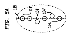
例えば、図1に見られる1つの従来の超小型電子パッケージ12において、パッケージ基板20の第1の周縁部16に隣接して端子の3つの列14を配置することができ、パッケージ基板20の第2の周縁部22に隣接して端子の別の3つの列18を配置することができる。従来のパッケージにおけるパッケージ基板20の中央領域24には、端子の列は全くない。図1は更に、パッケージ内の、面28上に素子コンタクト26を有する半導体チップ11を示す。素子コンタクト26は、パッケージ基板20の中央領域24における開口部、例えばボンドウインドウ、を通って延在するワイヤボンド30を通じて、パッケージ12の端子の列14、18と電気的に相互接続されている。場合によっては、超小型電子素子11の面28と基板20との間に接着層32を配置して、ワイヤボンドが接着層32の開口部を通って延在する状態で、超小型電子素子と基板との機械的接続を補強することができる。
For example, in one conventional
上記に鑑みて、特にそのようなパッケージと、そのようなパッケージを搭載し互いに電気的に相互接続することができる回路パネルとを含むアセンブリにおいて電気的性能を改善するために、超小型電子パッケージ上で端子の配置の改善をいくらか行うことができる。 In view of the above, in order to improve the electrical performance in an assembly comprising in particular such a package and a circuit panel on which such a package is mounted and can be electrically interconnected with each other, on a microelectronic package Can do some improvement in terminal placement.
本発明の態様によれば、超小型電子パッケージが、面及び該面において露出する複数の素子コンタクトを有する超小型電子素子と、互いに反対側の第1の表面及び第2の表面を有する基板と、前記超小型電子パッケージを該パッケージの外部にある少なくとも1つの構成要素に接続するように構成される、前記第2の表面において露出する複数の端子とを備えることができる。前記超小型電子素子はメモリ記憶アレイ機能を有することができる。前記基板は、前記超小型電子素子の素子コンタクトに向きかつ該素子コンタクトに接合される、第1の表面において露出する1組の基板コンタクトを有することができる。 According to an aspect of the present invention, a microelectronic package includes a microelectronic device having a surface and a plurality of device contacts exposed on the surface, and a substrate having a first surface and a second surface opposite to each other. A plurality of terminals exposed at the second surface configured to connect the microelectronic package to at least one component external to the package. The microelectronic element may have a memory storage array function. The substrate may have a set of substrate contacts exposed at a first surface that face the element contact of the microelectronic element and are bonded to the element contact.
前記端子は、前記基板コンタクトに電気的に接続することができ、複数の第1の端子を含むことができる。前記第1の端子は、理論的軸の第1の側に配置された第1の端子の第1の組と、前記第1の側と反対側の前記軸の第2の側に配置された前記第1の端子の第2の組とを含むことができる。前記第1の組及び前記第2の組のそれぞれは、前記超小型電子素子のメモリ記憶アレイの全ての利用可能なアドレス指定可能メモリ位置の中からアドレス指定可能メモリ位置を決定するのに前記超小型電子パッケージ内の回路によって使用可能なアドレス情報を運ぶように構成することができる。第1の組内の第1の端子の信号割当ては、第2の組内の第1の端子の信号割当ての鏡像とすることができる。 The terminal may be electrically connected to the substrate contact and may include a plurality of first terminals. The first terminal is disposed on a first set of first terminals disposed on a first side of a theoretical axis and on a second side of the shaft opposite the first side. And a second set of the first terminals. Each of the first set and the second set may be used to determine an addressable memory location from among all available addressable memory locations of the microelectronic memory storage array. It can be configured to carry address information that can be used by circuitry in a small electronic package. The signal assignment of the first terminal in the first set may be a mirror image of the signal assignment of the first terminal in the second set.
一例において、前記超小型電子素子は、メモリ記憶アレイ機能を提供する能動素子の数をいかなる他の機能よりも多く具体化することができる。例示的な実施形態において、第1の組及び第2の組のそれぞれの前記第1の端子は、前記アドレス指定可能メモリ位置を決定するのに前記超小型電子パッケージ内の前記回路によって使用可能な前記アドレス情報の全てを運ぶように構成することができる。一例において、第1の組及び第2の組のそれぞれの前記第1の端子は、前記超小型電子素子の動作モードを制御する情報を運ぶように構成することができる。特定の実施形態において、第1の組及び第2の組のそれぞれの前記第1の端子は、前記超小型電子パッケージに転送されるコマンド信号の全てを運ぶように構成することができ、前記コマンド信号は、ライトイネーブル(書き込み許可)、行アドレスストローブ、及び列アドレスストローブ信号である。 In one example, the microelectronic element may embody more active elements that provide a memory storage array function than any other function. In an exemplary embodiment, the first terminal of each of a first set and a second set can be used by the circuitry in the microelectronic package to determine the addressable memory location. It can be configured to carry all of the address information. In one example, the first terminal of each of the first set and the second set can be configured to carry information that controls an operating mode of the microelectronic element. In certain embodiments, the first terminals of each of the first set and the second set can be configured to carry all of the command signals transferred to the microelectronic package, and the command The signals are a write enable (write permission), a row address strobe, and a column address strobe signal.
一実施形態において、第1の組及び第2の組のそれぞれの前記第1の端子は、前記超小型電子パッケージに転送されるクロック信号を運ぶように構成することができ、前記クロック信号は、前記アドレス情報を運ぶ信号をサンプリングするのに使用されるクロックである。特定の例において、第1の組及び第2の組のそれぞれの前記第1の端子は、前記超小型電子パッケージに転送されるバンクアドレス信号の全てを運ぶように構成することができる。一例において、前記素子コンタクトは、前記超小型電子素子の前面において露出する再分配コンタクトを含むことができる。各再分配コンタクトは、トレース又はビアの少なくとも一方を通して前記超小型電子素子のコンタクトパッドに電気的に接続することができる。 In one embodiment, the first terminal of each of the first set and the second set can be configured to carry a clock signal that is transferred to the microelectronic package, wherein the clock signal is A clock used to sample the signal carrying the address information. In a particular example, the first terminal of each of a first set and a second set can be configured to carry all of the bank address signals transferred to the microelectronic package. In one example, the device contact can include a redistribution contact exposed at the front surface of the microelectronic device. Each redistribution contact can be electrically connected to a contact pad of the microelectronic element through at least one of a trace or a via.
特定の例において、前記第1の組及び第2の組の前記第1の端子は、それぞれの第1のグリッド及び第2のグリッド内の場所に配置することができる。前記第1のグリッド及び前記第2のグリッド内の端子の列は、前記基板の対向する第1の縁部及び第2の縁部に平行な方向に延在することができる。前記軸は、前記基板の前記第1の縁部及び前記第2の縁部に平行でかつ前記基板の前記第1の縁部及び前記第2の縁部から等距離のラインから、前記第1の端子の任意の2つの隣接する列間の最小ピッチの3.5倍以下の距離とすることができる。一実施形態において、少なくともいくつかの第1の端子を含む特定の列の大部分の端子の中心を通って延在する列軸は、前記特定の列の端子の1つ又は複数の端子の中心を通って延在しないことができる。 In a particular example, the first terminals of the first set and the second set may be located at locations within the respective first grid and second grid. The row of terminals in the first grid and the second grid may extend in a direction parallel to the opposing first and second edges of the substrate. The axis is parallel to the first edge and the second edge of the substrate and from a line equidistant from the first edge and the second edge of the substrate. The distance can be no greater than 3.5 times the minimum pitch between any two adjacent rows of terminals. In one embodiment, the column axis extending through the center of most terminals of a particular row including at least some first terminals is the center of one or more terminals of the particular row of terminals. Can not extend through.
一例において、前記列軸は、前記列の中央に置かれない前記1つ又は複数の端子の少なくとも1つの端子を通って延在しないことができる。特定の実施形態において、前記第1の組及び前記第2の組の前記第1の端子は、それぞれの第1のグリッド及び第2のグリッド内の場所に配置することができ、前記第1のグリッド及び前記第2のグリッドのそれぞれは、前記第1の端子の平行な第1の列及び第2の列を含むことができる。例示的な実施形態において、前記第1のグリッド又は前記第2のグリッドの少なくとも一方のグリッドは、前記少なくとも一方のグリッドの平行な前記第1の列と前記第2の列との間に少なくとも1つの端子を含むことができる。一実施形態において、前記端子は第2の端子を含むことができる。前記第2の端子の少なくともいくつかは、アドレス情報以外の情報を運ぶように構成することができる。特定の例において、前記第1の組及び前記第2の組の前記第1の端子は、それぞれの第1のグリッド及び第2のグリッド内の場所に配置することができ、前記第2の端子は、前記第1のグリッド及び前記第2のグリッド内ではなく、前記第2の表面上の場所に配置することができる。一例において、前記第1の組及び前記第2の組の前記第1の端子は、それぞれの第1のグリッド及び第2のグリッド内の場所に配置することができ、前記第2の端子の少なくともいくつかは、前記第1のグリッド及び前記第2のグリッド内に配置することができる。 In one example, the column axis may not extend through at least one terminal of the one or more terminals that are not centered in the column. In certain embodiments, the first terminals of the first set and the second set can be located at locations within the respective first grid and second grid, and the first set Each of the grid and the second grid may include a parallel first row and second row of the first terminals. In an exemplary embodiment, at least one grid of the first grid or the second grid is at least 1 between the parallel first and second columns of the at least one grid. One terminal can be included. In one embodiment, the terminal may include a second terminal. At least some of the second terminals can be configured to carry information other than address information. In a particular example, the first terminals of the first set and the second set can be located at locations within the respective first grid and second grid, and the second terminals May be located at a location on the second surface rather than within the first grid and the second grid. In one example, the first terminals of the first set and the second set can be disposed at locations within the respective first grid and second grid, and at least of the second terminals. Some can be placed in the first grid and the second grid.
特定の実施形態において、前記第1の組及び前記第2の組の前記第1の端子は、それぞれの第1のグリッド及び第2のグリッド内の場所に配置することができ、前記第2の端子の1つの部分は第3のグリッド内に配置することができ、前記第2の端子の別の部分は第4のグリッド内に配置することができる。前記第3のグリッド及び前記第4のグリッド内の端子の列は、互いに、また、前記第1のグリッド及び前記第2のグリッド内の端子の列に平行にすることができる。前記第3のグリッド内の前記第2の端子の信号割当ては、前記第4のグリッド内の前記第2の端子の信号割当ての鏡像とすることができる。一例において、前記第1のグリッド及び前記第2のグリッドは、前記第3のグリッド及び前記第4のグリッドを互いから分離することができる。 In certain embodiments, the first terminals of the first set and the second set can be disposed at locations within the respective first grid and second grid, and the second set One part of the terminals can be arranged in the third grid and another part of the second terminals can be arranged in the fourth grid. The rows of terminals in the third grid and the fourth grid may be parallel to each other and to the rows of terminals in the first grid and the second grid. The signal assignment of the second terminal in the third grid may be a mirror image of the signal assignment of the second terminal in the fourth grid. In one example, the first grid and the second grid can separate the third grid and the fourth grid from each other.
例示的な実施形態において、前記第2の端子の或る部分は第5のグリッド内に配置することができ、前記第2の端子の別の部分は第6のグリッド内に配置することができる。前記第5のグリッド及び前記第6のグリッド内の端子の列は、互いに平行とすることができ、前記第1の端子及び前記第2の端子の端子列が延在する第1の方向を横切る第2の方向に延在することができる。前記第5のグリッド内の前記第2の端子の信号割当ては、前記第1のグリッドと前記2のグリッドとの間の軸について対称とすることができ、前記第6のグリッド内の前記第2の端子の信号割当ては、前記第1のグリッドと前記2のグリッドとの間の軸について対称とすることができる。前記軸は、前記基板の対向する第1の縁部及び第2の縁部から等距離にあることができる。一例において、前記パッケージの外部にある前記少なくとも1つの構成要素は回路パネルとすることができる。特定の例において、超小型電子パッケージは、前記基板の前記第1の表面に向く表面を有するバッファチップを更に備えることができる。前記バッファチップは、前記第1の組及び前記第2の組の少なくとも一方の組の前記第1の端子に電気的に接続することができる。前記バッファチップは、前記第1の端子で受信された前記アドレス情報の少なくとも一部を再生し、前記再生された信号を前記超小型電子素子に出力するように構成することができる。 In an exemplary embodiment, a portion of the second terminal can be placed in a fifth grid and another portion of the second terminal can be placed in a sixth grid. . The rows of terminals in the fifth grid and the sixth grid may be parallel to each other and cross a first direction in which the terminal rows of the first terminal and the second terminal extend. It can extend in the second direction. The signal assignment of the second terminal in the fifth grid may be symmetric about an axis between the first grid and the second grid, and the second assignment in the sixth grid. The signal assignments of the terminals may be symmetric about an axis between the first grid and the second grid. The axis can be equidistant from the opposing first and second edges of the substrate. In one example, the at least one component external to the package can be a circuit panel. In a particular example, the microelectronic package can further comprise a buffer chip having a surface facing the first surface of the substrate. The buffer chip can be electrically connected to the first terminal of at least one of the first set and the second set. The buffer chip may be configured to reproduce at least part of the address information received at the first terminal and output the reproduced signal to the microelectronic element.
一実施形態において、前記超小型電子素子は第1の超小型電子素子とすることができ、基板コンタクトの前記組は基板コンタクトの第1の組とすることができる。前記超小型電子パッケージは、面及び該面において露出する複数の素子コンタクトを有する第2の超小型電子素子を更に備えることができる。前記第2の超小型電子素子はメモリ記憶アレイ機能を有することができる。前記基板は、前記第2の超小型電子素子の素子コンタクトに向きかつ該第2の超小型電子素子の該素子コンタクトに接合される、前記第1の表面において露出する基板コンタクトの第2の組を有することができる。前記端子は、基板コンタクトの前記第2の組に電気的に接続することができる。前記第1の組及び前記第2の組のそれぞれの前記第1の端子は、前記第1の超小型電子素子及び前記第2の超小型電子素子の少なくとも一方の超小型電子素子のメモリ記憶アレイの全ての利用可能なアドレス指定可能メモリ位置の中からアドレス指定可能メモリ位置を決定するのに前記超小型電子パッケージ内の回路によって使用可能なアドレス情報を運ぶように構成することができる。 In one embodiment, the microelectronic element may be a first microelectronic element and the set of substrate contacts may be a first set of substrate contacts. The microelectronic package may further include a second microelectronic device having a surface and a plurality of device contacts exposed on the surface. The second microelectronic element may have a memory storage array function. A second set of substrate contacts exposed at the first surface facing the element contact of the second microelectronic element and bonded to the element contact of the second microelectronic element; Can have. The terminals can be electrically connected to the second set of substrate contacts. The first terminal of each of the first set and the second set is a memory storage array of at least one microelectronic element of the first microelectronic element and the second microelectronic element. Can be configured to carry address information that can be used by circuitry within the microelectronic package to determine an addressable memory location from among all available addressable memory locations.
特定の例において、前記第1の超小型電子素子及び前記第2の超小型電子素子の前記面は、前記基板の前記第1の表面に平行な単一平面内に配置することができる。一実施形態において、前記第1の組の前記第1の端子は、前記第1の超小型電子素子に電気的に接続することができ、前記第2の組の前記第1の端子は、前記第2の超小型電子素子に電気的に接続することができる。特定の実施形態において、前記第1の組及び前記第2の組の前記第1の端子は、前記第1の超小型電子素子及び前記第2の超小型電子素子のそれぞれに電気的に接続することができる。 In a particular example, the surfaces of the first microelectronic element and the second microelectronic element can be arranged in a single plane parallel to the first surface of the substrate. In one embodiment, the first terminal of the first set can be electrically connected to the first microelectronic element, and the first terminal of the second set is It can be electrically connected to the second microelectronic element. In a specific embodiment, the first terminals of the first set and the second set are electrically connected to the first microelectronic element and the second microelectronic element, respectively. be able to.
一例において、前記第1の組の前記第1の端子は、前記第1の超小型電子素子に電気的に接続することができ、前記第2の超小型電子素子に電気的に接続しないことができる。前記第2の組の前記第1の端子は、前記第2の超小型電子素子に電気的に接続することができ、前記第1の超小型電子素子に電気的に接続しないことができる。例示的な実施形態において、前記基板は、誘電体素子の平面において30パーツパーミリオン/摂氏温度(「ppm/℃」)未満の熱膨張率(「CTE」)を有する、前記誘電体素子を含むことができる。一例において、前記基板は、12ppm/℃未満のCTEを有する素子を含むことができる。 In one example, the first terminal of the first set may be electrically connected to the first microelectronic element and not electrically connected to the second microelectronic element. it can. The first terminals of the second set may be electrically connected to the second microelectronic element and may not be electrically connected to the first microelectronic element. In an exemplary embodiment, the substrate includes the dielectric element having a coefficient of thermal expansion (“CTE”) of less than 30 parts per million / degrees Celsius (“ppm / ° C.”) in the plane of the dielectric element. be able to. In one example, the substrate can include a device having a CTE of less than 12 ppm / ° C.
本発明の別の態様によれば、超小型電子パッケージが、面及び該面上の複数の素子コンタクトを有する超小型電子素子と、互いに反対側の第1の表面及び第2の表面を有する基板と、超小型電子パッケージを該パッケージの外部にある少なくとも1つの構成要素に接続させるために構成される前記第2の表面において露出する複数の端子とを備えることができる。前記超小型電子素子は、メモリ記憶アレイ機能を提供する能動素子の数をいかなる他の機能よりも多く具体化することができる。前記基板は、前記超小型電子素子の素子コンタクトに向きかつ素子コンタクトに接合される、第1の表面上の基板コンタクトの組を有することができる。 According to another aspect of the present invention, a microelectronic package includes a microelectronic device having a surface and a plurality of device contacts on the surface, and a substrate having first and second surfaces opposite to each other. And a plurality of terminals exposed at the second surface configured to connect the microelectronic package to at least one component external to the package. The microelectronic element may embody more active elements that provide a memory storage array function than any other function. The substrate may have a set of substrate contacts on a first surface that face the element contact of the microelectronic element and are bonded to the element contact.
前記端子は、前記基板コンタクトに電気的に接続することができ、平行な第1のグリッド及び第2のグリッド内の場所に配置された第1の端子を含むことができる。第1のグリッド及び第2のグリッドのそれぞれの前記第1の端子は、前記超小型電子素子内のメモリ記憶アレイの全ての利用可能なアドレス指定可能メモリ位置の中からアドレス指定可能メモリ位置を決定するのに超小型電子パッケージ内の回路によって使用可能なアドレス情報の大部分を運ぶように構成することができる。前記第1のグリッド内の前記第1の端子の信号割当ては、前記第2のグリッド内の前記第1の端子の信号割当ての鏡像とすることができる。特定の実施形態では、前記第1のグリッド及び前記第2のグリッドのそれぞれの前記第1の端子は、前記アドレス指定可能メモリ位置を決定するのに超小型電子パッケージ内の回路によって使用可能なアドレス情報の少なくとも3/4を運ぶように構成することができる。 The terminal can be electrically connected to the substrate contact and can include a first terminal disposed at a location in a parallel first grid and a second grid. The first terminal of each of the first grid and the second grid determines an addressable memory location from among all available addressable memory locations of a memory storage array in the microelectronic element. In doing so, it can be configured to carry most of the address information that can be used by the circuitry in the microelectronic package. The signal assignment of the first terminal in the first grid may be a mirror image of the signal assignment of the first terminal in the second grid. In certain embodiments, the first terminal of each of the first grid and the second grid is an address that can be used by circuitry in a microelectronic package to determine the addressable memory location. It can be configured to carry at least 3/4 of the information.
図1に関して説明する例示的な従来の超小型電子パッケージ12に鑑みて、本発明者らは、メモリ記憶アレイチップを組み込む超小型電子パッケージ及びそのような超小型電子パッケージを組み込む超小型電子アセンブリの電気的性能を改善するのに役立てることができる、行うことができる改善を認識した。
In view of the exemplary conventional
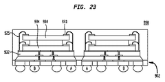
特に、図2〜図4に示すもの等のアセンブリ内に設けられた場合の超小型電子パッケージの使用に関して改善を行うことができる。図2〜図4において、パッケージ12Aが回路パネルの表面に搭載され、別の同様なパッケージ12Bが回路パネルの反対側の表面上に、それに向き合って搭載される。パッケージ12A、12Bは通常、機能的及び機械的に互いに同等である。機能的及び機械的に同等なパッケージの他の対12Cと12D、及び12Eと12Fもまた、通常同じ回路パネル34に搭載される。回路パネルとそれに取り付けられたパッケージとは、一般にデュアルインラインメモリモジュール(「DIMM」)と呼ばれるアセンブリの一部を形成することができる。対向して搭載されたパッケージの対それぞれにおけるパッケージ、例えばパッケージ12A、12Bは、回路パネルの反対に位置する表面上のコンタクトに接続し、それぞれの対におけるパッケージ同士が通常それぞれの面積の90%よりも多く互いに重なるようになっている。回路パネル34内のローカル配線は、端子、例えばそれぞれのパッケージ上の「1」、「5」とラベルがついた端子を回路パネル上のグローバル配線に接続する。グローバル配線は、位置I、II、及びIII等の回路パネル34上の接続位置にいくつかの信号を伝えるのに用いる、バス36の信号導体を含む。例えば、パッケージ12A、12Bは、接続位置Iに結合したローカル配線によってバス36に電気的に接続され、パッケージ12C、12Dは、接続位置IIに結合したローカル配線によってバスに電気的に接続され、パッケージ12E、12Fは、接続位置IIIに結合したローカル配線によってバスに電気的に接続される。
In particular, improvements can be made with respect to the use of microelectronic packages when provided in assemblies such as those shown in FIGS. 2-4, a
回路パネル34は、パッケージ12Aの一方の縁部16近くの「1」とラベルがついた端子が回路パネル34を貫いてパッケージ12Bの同じ縁部16近くのパッケージ12Bの「1」とラベルがついた端子に接続する、十文字すなわち「シューレース(靴ひも)」パターンと同様に見えるローカル相互接続配線を用いて、パッケージ12A、12Bそれぞれの端子を電気的に相互接続する。しかし、回路パネル34に取り付けたパッケージ12Bの縁部16は、パッケージ12Aの縁部16から遠い。図2〜図4は、パッケージ12Aの縁部22近くの「5」とラベルがついた端子が回路パネル34を貫いてパッケージ12Bの同じ縁部22近くのパッケージ12Bの「5」とラベルがついた端子に接続するということを更に示す。アセンブリ38において、パッケージ12Aの縁部22はパッケージ12Bの縁部22から遠い。
The
回路パネルを貫く、各パッケージ、例えばパッケージ12A上の端子と、その反対側に搭載されたパッケージ、すなわちパッケージ12B上の対応する端子との間の接続は、かなり長いものである。図3において更にわかるように、同様の超小型電子パッケージ12A、12Bのそのようなアセンブリにおいて、回路パネル34は、バス36の信号導体を、バスからの同じ信号がそれぞれのパッケージに送信されることになっている場合には、「1」と印がついたパッケージ12Aの端子及び「1」と印がついたパッケージ12Bの対応する端子と電気的に相互接続することができる。同様に回路パネル34は、バス36の別の信号導体を、「2」と印がついたパッケージ12Aの端子及び「2」と印がついたパッケージ12Bの対応する端子と電気的に相互接続することができる。同じ接続の仕組みを、バスの他の信号導体及びそれぞれのパッケージの対応する端子にも当てはめることができる。
The connection between each package, eg the terminal on the
回路パネル34上のバス36と、パッケージのそれぞれの対、例えば、基板の接続位置Iにおけるパッケージ12A、12B(図2)、のそれぞれのパッケージとの間のローカル配線は、非終端スタブの形とすることができる。そのようなローカル配線は、比較的長い場合には、場合によっては後述するようにアセンブリ38の性能に影響を及ぼす場合がある。さらに、回路パネル34はまたローカル配線に、他のパッケージ、すなわちパッケージの対12C及び12D並びにパッケージの対12E及び12Fの或る特定の端子をバス36のグローバル配線に電気的に相互接続するよう求め、そのような配線も、同じようにアセンブリの性能に影響を及ぼす可能性がある。
The local wiring between the bus 36 on the
図4は更に、信号「1」、「2」、「3」、「4」、「5」、「6」、「7」、及び「8」を運ぶよう割り当てられた端子のそれぞれの対の超小型電子パッケージ12Aと12Bとの間の相互接続を示す。図4においてわかるように、端子の、基板の表面の中央領域24内ではなく、列14、18の全ては各パッケージ12A、12Bそれぞれの縁部16、22の近くに露出するので、端子の列14、18が延在する方向42を横切る方向40に回路パネル34を横切るのに必要な配線は、非常に長くなる可能性がある。DRAMチップの長さは、それぞれの辺において10ミリメートルの範囲にすることができるということを認識すれば、或る信号が、2つの対向して搭載されるパッケージ12A、12Bの対応する端子に同じ信号をルーティングするのに必要な、図2〜図4に見られるアセンブリ38における回路パネル34内のローカル配線の長さは、5ミリメートルから10ミリメートルの間に及ぶ可能性があり、通常約7ミリメートルとすることができる。
FIG. 4 further illustrates each pair of terminals assigned to carry signals “1”, “2”, “3”, “4”, “5”, “6”, “7”, and “8”. Fig. 4 illustrates the interconnection between the
場合によっては、パッケージの端子同士を接続する回路パネル上の非終端配線が比較的長くても、アセンブリ38の電気的性能にひどく影響を及ぼすことはない場合がある。しかし、図2に示すように、回路パネルのバス36から回路パネルに接続されたパッケージの多数の対のそれぞれに信号を転送する場合、バス36からそこに接続されたそれぞれのパッケージ上の端子まで延在するスタブ、すなわちローカル配線の電気長がアセンブリ38の性能に潜在的に影響を及ぼすということを本発明者らは認識している。非終端スタブ上の信号反射は、それぞれのパッケージの接続された端子から戻ってバス36上へと逆方向に伝わり、したがってバス36からパッケージに転送される信号を劣化させてしまう可能性がある。この影響は、現在製造される超小型電子素子を含むいくつかのパッケージについては許容できる場合がある。しかし、増大する信号スイッチング周波数もしくは低電圧スイング信号又はその両方で動作する現在又は将来のアセンブリにおいては、この影響は甚だしくなる可能性がある、ということを本発明者は認識している。これらのアセンブリについては、送信信号のセトリングタイム(整定時間)、リンギング、ジッタ、又は符号間干渉が受け入れがたい程度まで増大する場合がある。
In some cases, the relatively long unterminated wiring on the circuit panel that connects the terminals of the package may not significantly affect the electrical performance of the
本発明者らは、非終端スタブの電気長は通常、回路パネルのバス36を、そこに搭載されたパッケージの端子と接続するローカル配線よりも長いということを更に認識している。それぞれのパッケージ内の、パッケージ端子から内部の半導体チップまでの非終端配線によって、スタブ長さが増加する。 The inventors have further recognized that the electrical length of the unterminated stub is typically longer than the local wiring connecting the circuit panel bus 36 with the terminals of the package mounted therein. The stub length is increased by the non-terminal wiring from the package terminal to the internal semiconductor chip in each package.
特定の例において、バス36は、DIMM等の主流のメモリ記憶アレイ機能を有するアセンブリのコマンド−アドレスバスである。コマンド−アドレスバス36は、パッケージ内の回路、例えば、行アドレス及び列アドレスのデコーダ、並びにもしある場合にはバンク選択回路が使用して、パッケージにおける超小型電子素子内のメモリ記憶アレイの全ての利用可能なアドレス指定可能メモリ位置からアドレス指定可能メモリ位置を決定することができる、超小型電子パッケージに転送されるアドレス情報を運ぶように構成することができる。コマンド−アドレスバス36は、接続位置、例えば、図2に示す位置I、II、及びIIIに上述のアドレス情報を運ぶように構成することができる。これらの上述のアドレス情報は次に、ローカル配線によって、そこにパッケージ12A、12B、12C、12D、12E及び12Fが接続される回路パネルの互いに反対側の表面上のパネルコンタクトのそれぞれの組に分配することができる。
In a particular example, bus 36 is a command-address bus for an assembly having mainstream memory storage array functionality, such as a DIMM. The command-address bus 36 is used by circuits in the package, such as row and column address decoders, and, if any, bank selection circuitry to all memory storage arrays in the microelectronic elements in the package. The addressable memory location can be determined from the available addressable memory locations and can be configured to carry address information that is transferred to the microelectronic package. The command-address bus 36 may be configured to carry the address information described above at a connection location, eg, locations I, II, and III shown in FIG. These above address information is then distributed by local wiring to respective sets of panel contacts on opposite surfaces of the circuit panel to which the
特定の例において、超小型電子素子がDRAMチップであるかDRAMチップを含む場合、コマンド−アドレスバス36は、超小型電子パッケージに転送される超小型電子素子のコマンド−アドレスバスの1群の信号、すなわちコマンド信号、アドレス信号、バンクアドレス信号、及びクロック信号の全てを運ぶように構成することができ、このコマンド信号は、ライトイネーブル、行アドレスストローブ、及び列アドレスストローブ信号を含み、このクロック信号は、アドレス信号をサンプリングするのに用いるクロックである。クロック信号はさまざまなタイプとすることができるが、一実施形態において、これらの端子が運ぶクロック信号は、差動、すなわち、真の及び相補クロック信号として受け取られる差動クロック信号の1つ又は複数の対とすることができる。 In a particular example, if the microelectronic element is a DRAM chip or includes a DRAM chip, the command-address bus 36 is a group of signals of the command-address bus of the microelectronic element that is transferred to the microelectronic package. The command signal, address signal, bank address signal, and clock signal, all of which include a write enable, row address strobe, and column address strobe signal. Is a clock used to sample the address signal. Although the clock signals can be of various types, in one embodiment, the clock signals carried by these terminals are one or more of the differential clock signals received as differential, ie, true and complementary clock signals. It can be a pair.
したがって、本明細書において説明する本発明の或る特定の実施形態は、そのような第1のパッケージ及び第2のパッケージが回路パネル、例えば回路基板、モジュール基板若しくはカード、又はフレキシブル回路パネルの互いに反対側の表面上に互いに対向して搭載される場合にスタブの長さを短くできるように構成した、超小型電子パッケージを提供する。回路パネル上に互いに対向して搭載される第1の超小型電子パッケージ及び第2の超小型電子パッケージを組み込むアセンブリは、それぞれのパッケージ間のスタブ長さを著しく低減することができる。こうしたアセンブリ内のスタブ長を低減することは、なかでも、整定時間、リンギング、ジッタ、又は符号間干渉のうちの1つ又は複数を低減すること等によって電気性能を改善することができる。さらに、回路パネルの構造の単純化、又は回路パネルの設計若しくは製造の複雑性及びコストの低減、又は回路パネルの設計及び製造双方の複雑性及びコストの低減等、他の利点もまた得ることを可能にすることができる。 Accordingly, certain embodiments of the invention described herein are such that such a first package and a second package are each of a circuit panel, eg, a circuit board, a module board or card, or a flexible circuit panel. Provided is a microelectronic package configured so that the length of a stub can be shortened when mounted opposite to each other on the opposite surface. An assembly incorporating a first microelectronic package and a second microelectronic package mounted opposite each other on a circuit panel can significantly reduce the stub length between the respective packages. Reducing the stub length in such an assembly can improve electrical performance, such as by reducing one or more of settling time, ringing, jitter, or intersymbol interference, among others. In addition, other advantages such as simplification of the structure of the circuit panel, or reduction of the complexity and cost of design or manufacture of the circuit panel, or reduction of complexity and cost of both design and manufacture of the circuit panel may also be obtained. Can be possible.
本発明の或る特定の実施形態は、超小型電子素子、例えば半導体チップ又は半導体チップの積み重ねた配列が主としてメモリ記憶アレイ機能を提供するように構成された、パッケージ又は超小型電子アセンブリを提供する。そのような超小型電子素子において、メモリ記憶アレイ機能を提供するように構成され、すなわち組み立てられ他のデバイスと相互接続された、内部の能動素子、例えばトランジスタの数は、いかなる他の機能を提供するように構成された能動素子の数よりも多い。したがって、一例において、DRAMチップ等の超小型電子素子は、その主要な又は唯一の機能としてメモリ記憶アレイ機能を有することができる。代替的に、別の例において、そのような超小型電子素子は、混合した使用法を有することができ、メモリ記憶アレイ機能を提供するように構成した能動素子を組み込むことができ、また、なかでもプロセッサ機能又は信号プロセッサもしくはグラフィックスプロセッサの機能等、別の機能を提供するように構成された他の能動素子も組み込むことができる。この場合、超小型電子素子は依然として、メモリ記憶アレイ機能を提供するように構成された能動素子の数を超小型電子素子のいかなる他の機能よりも多く有することができる。 Certain embodiments of the present invention provide a package or microelectronic assembly in which microelectronic elements, such as semiconductor chips or stacked arrays of semiconductor chips, are configured primarily to provide memory storage array functionality. . In such a microelectronic element, the number of internal active elements, eg transistors, configured to provide a memory storage array function, ie assembled and interconnected with other devices, provides any other function More than the number of active elements configured to do so. Thus, in one example, a microelectronic element such as a DRAM chip may have a memory storage array function as its primary or sole function. Alternatively, in another example, such microelectronic elements can have mixed usage, can incorporate active elements configured to provide memory storage array functionality, and However, other active elements configured to provide other functions, such as processor functions or signal processor or graphics processor functions, may also be incorporated. In this case, the microelectronic element can still have more active elements configured to provide a memory storage array function than any other function of the microelectronic element.
超小型電子素子は、面上に素子コンタクトの複数の列を有する面を有する。いくつかの実施形態では、超小型電子素子はそれぞれ、基板にフリップチップ実装され、それにより、第1の超小型電子素子及び第2の超小型電子素子の素子コンタクトは、基板の第1の表面上の基板コンタクトのそれぞれの第1の組及び第2の組に向き、それぞれの第1の組及び第2の組に接合される。他の実施形態では、超小型電子素子は、基板に隣接し、基板に電気的に接続された第1の半導体チップと、第1の半導体チップに載り、第1の半導体チップに電気的に接続された1つ又は複数の第2の半導体チップとを備えることができ、第2の半導体チップはメモリ記憶アレイ機能を主に提供するように構成される。 The microelectronic element has a surface having a plurality of rows of element contacts on the surface. In some embodiments, each microelectronic element is flip-chip mounted to the substrate so that the device contacts of the first microelectronic device and the second microelectronic device are on the first surface of the substrate. Oriented to the respective first and second sets of substrate contacts on the top and joined to the respective first and second sets. In another embodiment, the microelectronic element is adjacent to the substrate and electrically connected to the substrate, and is mounted on the first semiconductor chip and electrically connected to the first semiconductor chip. One or more second semiconductor chips, wherein the second semiconductor chip is configured to primarily provide a memory storage array function.
超小型電子パッケージをパッケージの外部にある少なくとも1つの構成要素に接続するように構成される複数の端子を、基板の第2の表面上に設けることができる。基板コンタクトに電気的に接続される端子は、平行な第1のグリッド及び第2のグリッド内の場所に配置される第1の端子を含む。 A plurality of terminals configured to connect the microelectronic package to at least one component external to the package may be provided on the second surface of the substrate. The terminals that are electrically connected to the substrate contacts include a first terminal disposed at a location in the parallel first grid and the second grid.
本発明の或る特定の実施形態において、第1のグリッド及び第2のグリッドは、超小型電子パッケージに転送される超小型電子素子のコマンド−アドレスバスの1群の信号、すなわちコマンド信号、アドレス信号、バンクアドレス信号、及びクロック信号の全てを運ぶように構成され、このコマンド信号は、ライトイネーブル、行アドレスストローブ、及び列アドレスストローブ信号を含み、このクロック信号は、アドレス信号をサンプリングするのに用いるクロックである。クロック信号はさまざまなタイプとすることができるが、一実施形態において、これらの端子が運ぶクロック信号は、差動、又は、真の及び相補クロック信号として受け取られる差動クロック信号の1つ又は複数の対とすることができる。 In certain embodiments of the invention, the first grid and the second grid are a group of signals on a command-address bus of microelectronic elements that are transferred to the microelectronic package, ie, command signals, addresses. Configured to carry all of the signal, bank address signal, and clock signal, the command signal includes a write enable, row address strobe, and column address strobe signal, which clock signal is used to sample the address signal. This is the clock to use. Although the clock signal can be of various types, in one embodiment, the clock signal carried by these terminals is one or more of the differential clock signals received as differential or as true and complementary clock signals. It can be a pair.
回路パネル、例えばプリント回路基板、モジュールカード等の上で、コマンド−アドレスバスのこれらの上述の信号、すなわちコマンド信号、アドレス信号、バンクアドレス信号、及びクロック信号を、並列でそこに接続された多数の超小型電子パッケージに、バスにより伝達することができる。1つのグリッド内の信号割当てが他のグリッド内の信号割当ての鏡像である平行な第1のグリッド及び第2のグリッド内に第1の端子の2重の組を設けることによって、互いに対向して回路パネルに実装される第1の超小型電子パッケージ及び第2の超小型電子パッケージのアセンブリにおいてスタブの長さを低減することができる。 On a circuit panel, such as a printed circuit board, module card, etc., a number of these above-mentioned signals on the command-address bus, ie command signals, address signals, bank address signals, and clock signals, connected in parallel there It can be transmitted to a microelectronic package of the above by a bus. Opposing each other by providing a dual set of first terminals in the first grid and the second grid in which the signal assignment in one grid is a mirror image of the signal assignment in the other grid. The stub length can be reduced in the assembly of the first microelectronic package and the second microelectronic package mounted on the circuit panel.
第1の超小型電子パッケージ及び第2の超小型電子パッケージが回路パネルの互いに反対側の実装表面に実装され、回路パネルがそれらのパッケージを電気的に相互接続すると、第1のパッケージの第1のグリッドの第1の端子のそれぞれは、第1のグリッドの第1の端子が接続する第2のパッケージの第2の鏡像グリッドの対応する第1の端子の1ボールピッチの距離以内で位置合わせすることができる。すなわち、対応するグリッドは、回路パネルの実装表面の1つの実装表面に平行な直交するx及びy方向に、互いの1ボールピッチの距離以内で位置合わせすることができる。ボールピッチは、両方のパッケージ上の端子の任意の2つの隣接する平行な列間の最小ピッチより大きくない。加えて、第2のパッケージの第1のグリッドの第1の端子のそれぞれは、第1のグリッドの第1の端子が接続する第1のパッケージの第2の鏡像グリッドの対応する第1の端子の1ボールピッチの距離以内で位置合わせすることができる。結果として、第1のパッケージのそれぞれの第1の端子は、第2のパッケージの対応する第1の端子に電気的に接続することができ、反対側の回路パネル表面上の端子の各対の実装位置は、回路パネルの表面の1つの表面に平行な直交するx及びy方向に、互いの1ボールピッチの距離以内で位置合わせされる。 When the first microelectronic package and the second microelectronic package are mounted on opposite mounting surfaces of the circuit panel and the circuit panel electrically interconnects the packages, the first of the first package Each of the first terminals of the grid is aligned within one ball pitch distance of the corresponding first terminal of the second mirror image grid of the second package to which the first terminal of the first grid is connected. can do. That is, the corresponding grid can be aligned within the distance of one ball pitch from each other in the orthogonal x and y directions parallel to one mounting surface of the circuit panel mounting surface. The ball pitch is not greater than the minimum pitch between any two adjacent parallel rows of terminals on both packages. In addition, each of the first terminals of the first grid of the second package corresponds to the first terminal of the second mirror image grid of the first package to which the first terminal of the first grid is connected. Can be aligned within a distance of 1 ball pitch. As a result, each first terminal of the first package can be electrically connected to a corresponding first terminal of the second package, and each pair of terminals on the opposite circuit panel surface The mounting position is aligned within a distance of one ball pitch from each other in the orthogonal x and y directions parallel to one surface of the surface of the circuit panel.
場合によっては、互いに反対側の回路パネル表面上の接続された端子の各対の実装位置は、更に互いに一致する場合がある。したがって、第1のパッケージ及び第2のパッケージの電気的に接続された第1の端子の対間の回路パネルを通る電気接続の長さは、電気的に接続された第1の端子のこれらの対のそれぞれの対内の端子が、互いの上に載るか又は第1の回路パネル表面に沿って直交するx及びy方向に互いの1ボールピッチ以内で少なくとも位置合わせされることができる点で、大幅に低減することができる。 In some cases, the mounting positions of each pair of connected terminals on opposite circuit panel surfaces may further match each other. Thus, the length of the electrical connection through the circuit panel between the pair of electrically connected first terminals of the first package and the second package is the length of these electrically connected first terminals. The terminals in each pair of the pair can be at least aligned within one ball pitch of each other in the x and y directions that rest on each other or perpendicular along the first circuit panel surface, It can be greatly reduced.
回路パネル構成を、この構成を有するアセンブリにおいて同様に簡略化することができる。その理由は、第1の端子の電気的に接続された各対間のルーティングが、主に垂直方向、すなわち回路パネルの厚さを通る方向にあることができるからである。すなわち、回路パネルの互いに反対側の表面に実装されるパッケージの対応する第1の端子の各対を電気的に接続するには、回路パネル上の真っ直ぐな貫通ビア接続があれば十分とすることができる。 The circuit panel configuration can be similarly simplified in an assembly having this configuration. This is because the routing between each electrically connected pair of first terminals can be primarily in the vertical direction, i.e., through the thickness of the circuit panel. That is, a straight through via connection on the circuit panel is sufficient to electrically connect each pair of corresponding first terminals of the package mounted on opposite surfaces of the circuit panel. Can do.
さらに、超小型電子パッケージのそれぞれの対が接続される接続位置間の、第1の端子によって運ばれる上述の信号、例えばコマンド−アドレスバス信号から信号をルーティングするのに必要な回路パネル上の配線のルーティング層の数を減らすことを可能にすることができる。具体的には、そのような信号を回路パネルに沿ってルーティングするのに必要なルーティング層の数は、場合によっては、2つ以下のルーティング層まで減らすことができる。しかし、回路パネル上に、上述のアドレス又はコマンド−アドレスバス信号を運ぶルーティング層の数よりも多い数の、他の信号を運ぶルーティング層が存在することができる。 Furthermore, the wiring on the circuit panel necessary to route signals from the above-mentioned signals carried by the first terminals, for example command-address bus signals, between the connection positions to which the respective pairs of microelectronic packages are connected. It may be possible to reduce the number of routing layers. Specifically, the number of routing layers required to route such signals along a circuit panel can be reduced to no more than two routing layers in some cases. However, there can be more routing layers on the circuit panel carrying other signals than there are routing layers carrying the address or command-address bus signals described above.
超小型電子パッケージはまた、第1の端子以外の第2の端子も有することができ、そのような端子は通常、上述のアドレス又はコマンド−アドレスバス信号以外の信号を運ぶように構成されている。一例において、第2の端子は、データマスク及び並列終端をオン又はオフするのに用いる終端レジスタへのODTすなわち「オンダイターミネーション(オンダイ終端)」信号だけではなく、超小型電子素子への及び/又はそこからの一方向又は双方向のデータ信号、ならびにデータストローブ信号を運ぶのに用いる端子を含むことができる。チップセレクト、リセット、電源電圧、例えばVdd、Vddq、及び接地、例えばVss及びVssq等の信号又は基準電位は、第2の端子によって運ぶことができる。これらの信号又は基準電位のいずれも、第1の端子によって運ぶ必要はない。いくつかの実施形態において、上述のアドレス又はコマンド−アドレスバス信号以外の信号を運ぶように構成したいくつかの又は全ての端子を第2の端子として配置することが可能であり、パッケージ上のどちらの位置であっても配置することができる。 The microelectronic package may also have a second terminal other than the first terminal, such terminal typically configured to carry signals other than the address or command-address bus signals described above. . In one example, the second terminal is not only the ODT or “on-die termination” signal to the termination register used to turn on or off the data mask and parallel termination, but also to the microelectronic element and / or Terminals used to carry one-way or two-way data signals therefrom as well as data strobe signals may be included. Chip select, reset, power supply voltages such as Vdd, Vddq, and ground, such as signals such as Vss and Vssq, or reference potentials can be carried by the second terminal. None of these signals or reference potentials need be carried by the first terminal. In some embodiments, some or all of the terminals configured to carry signals other than the address or command-address bus signals described above can be arranged as the second terminal, and either on the package Even if it is the position of, it can arrange | position.
代替的に、いくつかの実施形態では、上記で述べたアドレス信号又はコマンド−アドレスバス信号以外の信号を運ぶように構成される一部又は全ての端子を、パッケージ上の端子の第1のグリッド及び第2の鏡像グリッド内に配置することが可能である。こうして、上述したように、対応する端子間で回路パネル上に設けられる電気接続のスタブ長を低減することを可能にすることができる。 Alternatively, in some embodiments, some or all terminals configured to carry signals other than the address signals or command-address bus signals described above are connected to a first grid of terminals on the package. And in the second mirror image grid. Thus, as described above, it is possible to reduce the stub length of the electrical connection provided on the circuit panel between the corresponding terminals.
他の実施形態では、上記で述べたアドレス信号又はコマンド−アドレスバス信号以外の信号を運ぶように構成される端子の一部又は全ては、パッケージ表面上の第3のグリッド内の第2の端子の組及び同じパッケージ表面上の第4のグリッド内の第2の端子の別の組として配置することができ、第3のグリッド内の第2の端子の信号割当ては第4のグリッド内の第2の端子の信号割当ての鏡像である。こうして、上述した第1のパッケージ及び第2のパッケージの対応する第1の端子間の接続と同様に、第1のパッケージ及び第2のパッケージの電気的に接続された第2の端子の対間の回路パネルを通る電気接続の長さは、大幅に低減することができる。或る例では、電気的に接続された第2の端子の対は、互いの1ボールピッチ以内で位置合わせされることができる。特定の例では、電気的に接続された第2の端子のこれらの対のそれぞれの対内の端子は、互いの上に載る、すなわち、互いに一致することができる。さらに、スタブ長を低減し、第1のパッケージと第2のパッケージとの間の接続のための回路パネルの構成を簡略化するための上述した利益と同様の利益を、超小型電子パッケージの第2の端子がこうして配置されるときに得ることができる。 In other embodiments, some or all of the terminals configured to carry signals other than the address signals or command-address bus signals described above are second terminals in a third grid on the package surface. And another set of second terminals in a fourth grid on the same package surface, the signal assignment of the second terminals in the third grid being the second in the fourth grid. 2 is a mirror image of the signal assignment of two terminals. Thus, as in the connection between the corresponding first terminals of the first package and the second package described above, between the pair of electrically connected second terminals of the first package and the second package. The length of the electrical connection through the circuit panel can be greatly reduced. In one example, the electrically connected second pair of terminals can be aligned within one ball pitch of each other. In a particular example, the terminals in each of these pairs of electrically connected second terminals can rest on each other, i.e., coincide with each other. In addition, the same benefits as described above for reducing the stub length and simplifying the configuration of the circuit panel for the connection between the first package and the second package, It can be obtained when two terminals are thus arranged.
そのため、本発明の或る実施形態による超小型電子パッケージ100は、図5、図6、及び図7に示される。図に見られるように、一例では、パッケージ100は、それぞれがメモリ記憶アレイ機能を有する第1の超小型電子素子101及び第2の超小型電子素子103を含むことができる。しかし、特定の例では、各超小型電子素子を、メモリ記憶アレイ機能を主に提供するように構成することができる。後者の場合、第1の超小型電子素子及び第2の超小型電子素子のそれぞれは、メモリ記憶アレイ機能を提供する能動素子、例えばトランジスタの数をいかなる他の機能よりも多く有することができる。
Thus, a
第1の超小型電子素子及び第2の超小型電子素子は、そのそれぞれの面105に素子コンタクト111、113を有する。1つのタイプのこうした超小型電子素子101、103では、素子コンタクト111、113のいくつかのコンタクトの各コンタクトは、超小型電子素子に供給される複数のアドレス信号のそれぞれのアドレス信号を受信することに専用にされる。この場合、こうしたコンタクト111、113のそれぞれは、外部から超小型電子素子101、103に供給される複数のアドレス信号のそれぞれの1つのアドレス信号を受信することができる。
The first microelectronic element and the second microelectronic element have
このタイプの超小型電子素子101、103の特定の一例において、それぞれの超小型電子素子が用いるクロックの縁部に対して、すなわち、異なる第1の電圧状態と第2の電圧状態との間でのクロックの遷移で、素子コンタクト111、113において存在する複数のアドレス信号のそれぞれをサンプリングすることができる。すなわち、それぞれのアドレス信号は、クロックのより低電圧の状態とより高電圧の状態との間の立ち上がり遷移において、又は、クロックのより高電圧の状態とより低電圧の状態との間の立ち下がり遷移においてサンプリングすることができる。したがって、複数のアドレス信号はクロックの立ち上がり遷移において全てサンプリングすることもできるし、そのようなアドレス信号はクロックの立ち下がり遷移において全てサンプリングすることもできるし、又は、別の例において、素子コンタクト111、113のうちの1つにおけるアドレス信号は、クロックの立ち上がり遷移においてサンプリングすることができ、別の1つの外部のコンタクトにおけるアドレス信号は、クロックの立ち下がり遷移においてサンプリングすることができる。
In a particular example of this type of
主としてメモリ記憶アレイ機能を提供するように構成した、別のタイプの超小型電子素子101、103において、その上のアドレスコンタクトのうちの1つ又は複数を多重方式で用いることができる。この例において、それぞれの超小型電子素子101、103の特定の素子コンタクト111、113は、外部から超小型電子素子に供給される2つ以上の互いに異なる信号を受け取ることができる。したがって、第1のアドレス信号は異なる第1の電圧状態と第2の電圧状態との間のクロックの第1の遷移(例えば、立ち上がり遷移)において、特定のコンタクト111、113においてサンプリングすることができ、第1のアドレス信号以外の信号は、第1の電圧状態と第2の電圧状態との間のクロックの、第1の遷移と反対の第2の遷移(例えば、立ち下がり遷移)において、特定のコンタクトにおいてサンプリングすることができる。
In another type of
そのような多重方式において、それぞれの超小型電子素子101、103の同じ素子コンタクト111、113上で、クロックの同じサイクル内で2つの異なる信号を受け取ることができる。特定の場合において、この方法での多重化によって、それぞれの超小型電子素子101、103の同じ素子コンタクト111、113上で、同じクロックサイクル内で第1のアドレス信号とそれとは異なる信号とを受け取ることができる。更に別の例において、この方法での多重化によって、第1のアドレス信号と、異なる第2のアドレス信号とを、それぞれの超小型電子素子101、103の同じ素子コンタクト111、113上で同じクロックサイクル内で受け取ることができる。
In such a multiplexing scheme, two different signals can be received within the same cycle of the clock on the
基板102は、誘電体素子122を含むことができ、誘電体素子は、場合によっては、本質的に、ポリマ材料、例えば、なかでも樹脂又はポリイミドからなることができる。代替的に、基板は、例えばBT樹脂又はFR−4構成のガラス繊維強化エポキシ等の複合構成を有する誘電体素子を含むことができる。いくつかの例では、誘電体素子は、誘電体素子の平面内で、すなわち、基板102の第1の表面108に平行な方向に、最大30パーツパーミリオン/摂氏温度(以降で「ppm/℃」)の熱膨張率を有する。別の例では、基板は、端子及び他の導電性構造がその上に配置される、12パーツパーミリオン/摂氏温度未満の熱膨張率(「CTE」)を有する材料の支持要素を含むことができる。例えば、こうした低CTE素子は、本質的に、ガラス材料、セラミック材料、半導体材料、若しくは液晶ポリマ材料、又はこうした材料の組合せからなることができる。
The
図6に見られるように、基板コンタクトの第1の組121及び第2の組123は、基板の第1の表面108において露出する。本明細書で使用されるように、導電性素子が、構造の表面「において露出する」という記述は、導電性素子が、構造の外側から表面に向かって表面に垂直な方向に移動する理論的な点に接触するために利用可能であることを示す。そのため、構造の表面において露出する端子又は他の導電性素子は、こうした表面から突出することができるか、こうした表面と同一平面上にあることができるか、又は、こうした表面に対して凹み、構造内の穴又は窪みを通して露出することができる。
As can be seen in FIG. 6, the
基板コンタクトの第1の組121は、第1の超小型電子素子の素子コンタクト111に向き、ボンドメタル、例えば、なかでもはんだ、錫、インジウム、共晶物、又は金か、他の導電性ボンド材料か、又はおそらくは考えられる構造の中でもとりわけ導電性バンプ又はマイクロピラー等の他の構造等によって、138にて素子コンタクト111に接合される。場合によっては、ダイ取付(ダイアタッチ)接着剤又はアンダーフィルを、超小型電子素子の面105と基板102の表面108との間に配置することができ、ダイ取付接着剤又はアンダーフィルは、超小型電子素子と基板との間の接続を機械的に強化することができ、超小型電子素子と基板との間の接合を機械的に支持することができる。
The
基板コンタクトの第2の組123は、第2の超小型電子素子の素子コンタクト113に向き、素子コンタクト113に接合される。図6に特に示す実施形態では、第1の超小型電子素子101及び第2の超小型電子素子103の面105は、基板102の第1の平面108に平行な単一平面112内に配置することができる。
The
図5に特に示すように、いくつかの実施形態では、超小型電子素子のコンタクトは、コンタクト111について示すように単一列で配置することができるか、又は、コンタクト113について示すように複数の列で配置することができる。各列は、方向134に沿う列の各垂直レイアウト位置にコンタクトを含むことができるか、又は、コンタクトは、コンタクト113の複数の列のうちの1つの列の場合のように、列の1つ又は複数の位置から欠落することができる。特定の実施形態では、コンタクトを、超小型電子素子の面105を覆ってエリアアレイで配置することができる。別の例では、超小型電子素子のコンタクトは、図5で超小型電子素子101、103の境界をマーク付けする破線で示す超小型電子素子の1つ又は複数の周辺縁部に隣接してコンタクトの1つ又は複数の組で配置することができる。特定の例では、超小型電子素子は単一半導体チップとすることができ、超小型電子素子上のコンタクト111又は113は、半導体チップのコンタクトである「チップコンタクト」とすることができる。別の例では、特定の超小型電子素子は、それぞれがチップコンタクトを有する1つ又は複数の半導体チップを含むことができ、コンタクト111又は113は、再分配コンタクトを含むことができ、再分配コンタクトは、超小型電子素子の面105上に形成され、また、例えばトレース及びビア等の導電性素子によってチップコンタクトに電気的に接続される。こうした超小型電子素子の例は、図26Dを参照して以下で述べられる。特に断らない限り、本明細書の例のそれぞれにおける超小型電子素子の「コンタクト」は、述べたこれらの方法の任意の方法で配置することができる。
As shown particularly in FIG. 5, in some embodiments, the contacts of the microelectronic element can be arranged in a single row as shown for
超小型電子素子101、若しくは超小型電子素子103、又はそれらの両方は、素子コンタクトの列内に配置されない場合がある更なるコンタクトも含むことができる。これらの更なるコンタクトを、電源、グラウンドに接続するために、又は、試験をするために使用することができるようなプロービングデバイスとの接触のために利用可能なコンタクトとして使用することができる。
The
図5に見られるように、パッケージ100は、例えば回路パネル等の、パッケージ100の外部の構成要素にパッケージ100を電気的かつ機械的に接続する、表面110において露出する第1の端子104及び第2の端子106を有することができる。端子104、106は、導電性パッド、ポスト、又は他の導電性構造とすることができる。図6に見られる例では、端子は、場合によっては、なかでもはんだ、錫、インジウム、金、若しくは共晶材料等のボンドメタル又は他の導電性ボンド材料を含むことができるような接合要素130を含むことができ、また場合によっては、導電性パッド又はポスト等の基板の導電性構造に取り付けられる導電性バンプ等の更なる構造も含むことができる。第1の端子104及び第2の端子106は、例えばトレース及びビア等の基板上の導電性構造を通して基板コンタクト121、123に電気的に接続することができる。
As seen in FIG. 5, the
第1の端子104の第1の組は、第1の表面108から反対の基板102の第2の表面110において露出する第1のグリッド114内の場所に配置することができる。第1の表面108及び第2の表面110は、反対方向に向き、したがって、互いに対して反対側にあり、「互いに反対側の表面」である。第1の端子104の第2の組は、基板の第2の表面110において露出する第2のグリッド124内の位置に配置することができる。図のいくつかでは、第1のグリッド及び第2のグリッドは、超小型電子素子の前面の外側境界を越えて延在するように示されるが、それは、必ずしも当てはまらない。本発明の或る特定の実施形態では、第1の端子の第1のグリッド及び第2のグリッド114、124のそれぞれは、コマンド−アドレスバスの或る特定の信号、すなわち、超小型電子パッケージ100内で動的メモリ記憶機能を提供するように構成される超小型電子素子101、103のアドレス信号の組の特に全ての信号を運ぶように構成することができる。
The first set of
例えば、超小型電子素子101、103がDRAM半導体チップを含むかDRAM半導体チップである場合、第1のグリッド114及び第2のグリッド124のそれぞれにおける第1の端子は、パッケージ内の回路が、例えば、行アドレス及び列アドレスのデコーダ、並びにもしある場合にはバンク選択回路が使用して、パッケージにおける超小型電子素子内のメモリ記憶アレイの全ての利用可能なアドレス指定可能メモリ位置からアドレス指定可能メモリ位置を決定することができる、超小型電子パッケージ100に転送される十分なアドレス情報を運ぶように構成される。特定の実施形態において、第1のグリッド114及び第2のグリッド124のそれぞれにおける第1の端子は、そのようなメモリ記憶アレイ内のアドレス指定可能メモリ位置を決定するのに超小型電子パッケージ100内のそのような回路が用いるアドレス情報の全てを運ぶように構成することができる。
For example, when the
そのような実施形態の変形形態において、第1のグリッド114及び第2のグリッド124のそれぞれにおける第1の端子は、そのようなメモリ記憶アレイ内のアドレス指定可能メモリ位置を決定するのに超小型電子パッケージ100内のそのような回路が用いるアドレス情報の大部分を運ぶように構成することができ、その場合には、超小型電子パッケージ上の上述の第2の端子106のうちの少なくともいくつか等、他の端子が、アドレス情報の残りの部分を運ぶように構成される。そのような変形形態において、特定の実施形態において、第1のグリッド114及び第2のグリッド124のそれぞれは、そのようなメモリ記憶アレイ内のアドレス指定可能メモリ位置を決定するのに超小型電子パッケージ100内のそのような回路が用いるアドレス情報の3/4以上を運ぶように構成される。
In a variation of such an embodiment, the first terminal in each of the
特定の実施形態において、第1のグリッド114及び第2のグリッド124のそれぞれはチップセレクト情報、例えば、チップ内のメモリ記憶位置にアクセスするために超小型電子パッケージ100内の特定のチップを選択するのに利用できる情報を運ぶように構成されない場合がある。別の実施形態において、第1のグリッド114及び第2のグリッド124のうちの少なくとも1つは、実際にチップセレクト情報を運ぶことができる。
In a particular embodiment, each of the
通常、超小型電子パッケージ100内の超小型電子素子101、103がDRAMチップを含む場合には、一実施形態におけるアドレス信号は、パッケージの外部の構成要素、例えば、後述の回路パネル154等の回路パネルからパッケージに転送される全てのアドレス信号を含むことができ、それを用いて超小型電子パッケージ内のランダムアクセスアドレス指定可能メモリ位置を決定してそこに読み取りアクセス、又は読み取りアクセス又は書き込みアクセスのどちらかを行う。
Usually, when the
第2の端子106のうちの少なくともいくつかは、第1のグリッド114及び第2のグリッド124の第1の端子104によって運ばれるアドレス信号以外の信号を運ぶように構成することができる。チップセレクト、リセット、電源電圧、例えばVdd、Vddq、並びに接地、例えばVss及びVssq等の信号又は基準電位は、第2の端子106によって運ぶことができる。本明細書において参照される実施形態のいずれにおいても、別段の記載がないがない限り、これらの信号又は基準電位のいずれも、第1の端子104によって運ぶ必要はない。
At least some of the
特定の実施形態において、各超小型電子パッケージの第1のグリッド114及び第2のグリッド124のそれぞれは、第1の超小型電子素子101及び第2の超小型電子素子103のうちの少なくとも1つの超小型電子素子の動作モードを制御する情報を運ぶように構成することができる。より具体的には、第1のグリッド114及び第2のグリッド124のそれぞれは、超小型電子パッケージ100に転送されるコマンド信号及び/又はクロック信号の特定の1組の全てを運ぶように構成することができる。そのような実施形態において、第1の端子104は、外部の構成要素から超小型電子パッケージ100に転送されるコマンド信号、アドレス信号、バンクアドレス信号、及びクロック信号の全てを運ぶように構成することができ、このコマンド信号は、行アドレスストローブ、列アドレスストローブ、及びライトイネーブルを含む。こうした実施形態では、例えば、図21に示す超小型電子素子901の1つの超小型電子素子等の複合構造を有する超小型電子素子内の第1のチップは、動作モードを制御する情報を再生するように構成することができる。それに対して代替的に又は付加的に、こうした複合超小型電子素子内の第1のチップは、超小型電子素子の動作モードを制御する情報を部分的に又は完全に復号化するように構成することができる。こうした実施形態では、それぞれの第2のチップは、アドレス情報、コマンド情報、又は、超小型電子素子の動作モードを制御する情報の1つ又は複数を完全に復号化するように構成することもしないこともできる。
In certain embodiments, each of the
超小型電子素子のうちの1つ又は複数がダイナミックランダムアクセスメモリ(「DRAM」)半導体チップ又はDRAMチップのアセンブリによって提供されるもの等のダイナミックメモリ記憶アレイ機能を提供するように構成される一実施形態においては、コマンド信号は、ライトイネーブル、行アドレスストローブ、及び列アドレスストローブ信号である。ODT(オンダイターミネーション)、チップセレクト、クロックイネーブル等の他の信号は、第1のグリッド114及び第2のグリッド124が運ぶ必要のあるコマンド信号の一部ではない。クロック信号は、アドレス信号をサンプリングするのに超小型電子素子のうちの1つ又は複数が用いるクロックとすることができる。例えば、図7において見られるように、 第1の端子104は、アドレス信号A0〜A15(A0及びA15を含む)、及びバンクアドレス信号BA0、BA1及びBA2だけでなく、クロック信号CK及びCKB、行アドレスストローブRAS、列アドレスストローブCAS、及びライトイネーブル信号WEも含むことができる。
One implementation in which one or more of the microelectronic elements are configured to provide dynamic memory storage array functionality, such as that provided by a dynamic random access memory ("DRAM") semiconductor chip or an assembly of DRAM chips In embodiments, the command signals are a write enable, a row address strobe, and a column address strobe signal. Other signals such as ODT (on-die termination), chip select, clock enable, etc. are not part of the command signals that the
この実施形態において、第2の端子106のうちの少なくともいくつかは、第1のグリッド114及び第2のグリッド124の第1の端子104によって運ばれる信号(コマンド信号、アドレス信号、及びクロック信号)以外の信号を運ぶように構成することができる。チップセレクト、リセット、電源電圧、例えばVdd、Vddq、並びに接地、例えばVss及びVssq等の信号又は基準電位は、第2の端子106によって運ぶことができる。本明細書において参照される実施形態のいずれにおいても、別段の記載がないがない限り、これらの信号又は基準電位のいずれも、第1の端子104によって運ぶ必要はない。
In this embodiment, at least some of the
別の実施形態において、超小型電子素子のうちの1つ又は複数が、例えばNANDフラッシュメモリ等、DRAM以外についての技術において実施されるメモリ記憶アレイ機能を提供するように構成される場合には、第1のグリッド114及び第2のグリッド124が運ぶ必要のある特定のコマンド信号は、DRAMの場合に運ぶ必要のある信号(ライトイネーブル、行アドレスストローブ、及び列アドレスストローブ信号)の群以外の、信号の異なる1組とすることができる。
In another embodiment, if one or more of the microelectronic elements are configured to provide memory storage array functionality implemented in technologies other than DRAM, such as NAND flash memory, for example, The specific command signals that the
一実施形態では、アドレス信号以外の信号を運ぶように構成される第2の端子106の少なくともいくつかは、第1のグリッド114及び第2のグリッド124内の位置に配置することができる。一例では、コマンド信号、アドレス信号、及びクロック信号以外の信号を運ぶように構成される第2の端子106の少なくともいくつかは、第1のグリッド114及び第2のグリッド124内の位置に配置することができる。図面において、第2の端子106の特定の構成を示すが、図示の特定の構成は例示の目的のためであり、限定するよう意図するものではない。例えば、第2の端子106は、電源又は接地信号に接続するように構成される端子も含むことができる。
In one embodiment, at least some of the
パッケージの第1のグリッド114及び第2のグリッド124内の第1の端子の配置構成は、図5〜図7に特に示される。一例では、各グリッド114、124は、端子の平行な第1の列及び第2の列136を含むことができる。各グリッド内の端子の平行な列136は互いに隣接することができる。代替的に、図5〜図7に示さないが、少なくとも1つの端子を、端子の第1の列と第2の列との間に配置することができる。図5Aに見られる等の別の例では、グリッドは、列軸119が、列の端子104の大部分を通って延在する、すなわち、列の端子104の大部分に対して中央に置かれる、端子の列を含むことができる。しかし、こうした列では、端子の1つ又は複数は、端子104’の場合と同様に、列軸119に対して中央に置かれない場合がある。この場合、これらの1つ又は複数の端子は、たとえこうした端子(複数可)が軸119に対して中央に置かれなくても、特定の列の一部と考えられる。その理由は、こうした端子が、任意の他の列の軸より、その特定の列の軸119に近いからである。列軸119は、列軸に対して中央に置かれないこれらの1つ又は複数の端子を通して延在することができるか、又は場合によっては、中央に置かれない端子は、列軸119が、列の中央に置かれないこれらの端子を通過しないように、列軸からより遠くにあることができる。1つの列内に、又は更に、グリッド内のそれぞれの列の列軸に対して中央に置かれない2つ以上の列内に、1つの、いくつかの、又は多くの端子が存在する場合がある。
The arrangement of the first terminals in the
さらに、端子のグリッドが、端子のリング、多角形、又は更に散乱分布のように形作られた配置構成等、列以外のグループ化で端子の配置構成を含むことが可能である。図6に示すように、封止剤146が、基板の第1の表面108上に載ることができ、そこで超小型電子素子101、103に接触することができる。場合によっては、封止剤は、基板102から離れる方を向く超小型電子素子の表面145上に載ることができる。
In addition, the terminal grid may include terminal arrangements in groups other than columns, such as arrangements shaped like terminal rings, polygons, or even scatter distributions. As shown in FIG. 6, an
図7に見られるように、第2のグリッド124内の位置にある第1の端子の第2の組内の第1の端子の信号割当ては、第1のグリッド114内のそれぞれの位置にある第1の端子の第1の組の信号割当て124の鏡像である。第1の組内の第1の端子の信号割当ては、第2の組内の対応する第1の端子の信号割当てに対応し、その鏡像である。換言すれば、第1のグリッド及び第2のグリッド内の第1の端子の信号割当ては、第1のグリッド114と第2のグリッド124との間の理論的軸132について対称であり、軸132は、この場合、第1の端子の列136が延在する方向134に延在する。第2のグリッド124内の信号割当てが第1のグリッド114内の信号割当ての鏡像である状態で、信号CK(クロック)を運ぶように割当てられる第1のグリッド114の第1の端子104は、信号CKを運ぶように割当てられる第2のグリッド124の対応する第1の端子104とグリッド内で同じ相対的垂直位置に(方向134に)ある。しかし、第1のグリッド114が2つの列136を含み、信号CKを運ぶように割当てられる第1のグリッド114の端子が、第1のグリッドの2つの列の中の左列内にあるので、鏡像配置構成は、信号CKを運ぶように割当てられる第2のグリッド124の対応する端子が、第2のグリッドの2つの列の中の右列136内にあることを要求する。
As seen in FIG. 7, the signal assignments of the first terminals in the second set of first terminals that are in positions within the
それに従った別の例において、第1の端子の第1のグリッド114及び第2のグリッド124のそれぞれの「A3」として示す、アドレス情報を運ぶように割り当てられた端子は、パッケージ100(図6)内の1つ又は複数の超小型電子素子の対応する「A3」と名前のついた素子コンタクトを指定するということが明白である。したがって、情報が同じ名前、例えば「A3」を有する素子コンタクトに転送される場合に通る第1の端子の第1の組及び第2の組のそれぞれにおけるパッケージの外部のそのような対応する第1の端子は、たとえ第1の組及び第2の組における対応する第1の端子の名前が異なっていようとも、鏡像の信号割り当てを有すると考えられる。したがって、一例において、第1の端子の第1の組及び第2の組のそれぞれにおいて、鏡像の信号割り当て、例えば、「A3」と指定された信号割り当てを有する第1の端子のそれぞれの組に割り当てられた信号が、超小型電子素子上の「A3」という名前を有する素子コンタクトに入力される情報を運ぶ端子を特定することが可能である。ただし、第1の組及び第2の組のそれぞれにおける対応する端子の名前は、例えば第1の組においてA3L(A3左)という名前を与え、第2の組においてA3R(A3右)と言う名前を与えることができる等、互いに異なることができる。
In another example according thereto, the terminals assigned to carry address information, indicated as “A3” in each of the
さらに、図7において「A3」で示す第1の端子の対応する対においてパッケージに提供されるアドレス情報は、場合によっては、超小型電子構造の外部の場所でのドライバ回路の同一の出力から生じることができる。その結果、信号「A3」を運ぶように割り当てられた(すなわち、上述のように、情報を超小型電子素子の「A3」と名前のついた素子コンタクトに転送するための)第1のグリッド114の第1の端子104は、信号「A3」を運ぶように割り当てられた第2のグリッド124の対応する第1の端子104と同じ、グリッド内での相対的垂直位置(方向134)にある。
Further, the address information provided to the package at the corresponding pair of first terminals, designated “A3” in FIG. 7, may in some cases result from the same output of the driver circuit at a location external to the microelectronic structure. be able to. As a result, the
この配列のもうひとつの結果は、信号WE(ライトイネーブル)を運ぶように割り当てられた端子もまた、第1のグリッド114及び第2のグリッド124のそれぞれにおいて同じ、グリッド内での相対的垂直位置にあるということである。しかし、第1のグリッド114において、WEを運ぶように割り当てられた端子は、第1のグリッドの2つの列136のうちの右側の列にあり、配列が鏡像であるためには、信号WEを運ぶように割り当てられた第2のグリッド124の対応する端子は、第2のグリッド124の2つの列のうちの左側の列136になければならない。図7においてわかることができるように、第1のグリッド及び第2のグリッドのそれぞれにおけるそれぞれの第1の端子について、少なくとも、上述のコマンド−アドレスバス信号を運ぶように割り当てられたそれぞれの第1の端子について、同じ関係が当てはまる。
Another result of this arrangement is that the terminals assigned to carry the signal WE (light enable) also have the same relative vertical position within the grid in each of the
第1の端子の信号割当てがその回りで対称である軸132は、基板上の種々の場所に位置することができる。特定の実施形態では、軸は、パッケージの中心軸であることができ、その中心軸は、特に、第1の端子の列136が縁部140、142に平行な方向に延在し、第1のグリッド及び第2のグリッドが、この中心軸について対称である位置に配置されるとき、基板の対向する第1の縁部及び第2の縁部140、142から等距離に位置付けられる。
The
代替的に、この対称軸132は、縁部140と142との間で等距離である中心軸から水平方向135にオフセットすることができる。一例では、軸132は、基板102の第1の縁部140及び第2の縁部142に平行でかつそれらから等距離にある中心軸又はラインからオフセットすることができ、オフセット距離は、第1の端子104の任意の2つの隣接する列間の最小ピッチの3.5倍以下の距離である。特定の実施形態では、第1のグリッド114及び第2のグリッド124のそれぞれグリッドの端子の少なくとも1つの列は、基板102の第1の縁部140及び第2の縁部142に平行でかつそれらから等距離にある中心軸又はラインからオフセット距離内に配置することができ、オフセット距離は、第1の端子104の任意の2つの隣接する列間の最小ピッチの3.5倍の距離である。
Alternatively, the axis of
特定の例において、第1のグリッド114の第1の端子104は、第1の超小型電子素子101と電気的に接続することができ、第2のグリッド124の第1の端子104は、第2の超小型電子素子103と電気的に接続することができる。そのような場合、第1のグリッド114の第1の端子104はまた、第2の超小型電子素子103と電気的に接続しないことができ、パッケージ100の第2のグリッド124の第1の端子104はまた、第1の超小型電子素子101と電気的に接続しないことができる。更に別の例において、第1のグリッド114及び第2のグリッドのそれぞれの第1の端子104は、第1の超小型電子素子101及び第2の超小型電子素子103のそれぞれと電気的に接続することができる。
In a particular example, the
上記で述べたように、第2の端子106は、コマンド−アドレスバスの上記で述べた信号以外の信号を運ぶように構成することができる。一例では、第2の端子106は、超小型電子素子への及び/又は超小型電子素子からの単方向又は双方向データ信号及びデータストローブ信号、並びに、データマスク信号及び終端抵抗に対して並列終端をオン又はオフにするために使用されるODT信号すなわち「オンダイ終端(on die termination)」信号を運ぶために使用される端子を含むことができる。チップセレクト、リセット、クロックイネーブル等の信号、並びに、電源電圧等の基準電位、例えばVdd、Vddq、又はグラウンド、例えばVss及びVssqは、第2の端子106によって運ぶことができ、信号又は基準電位はいずれも、第1の端子104によって運ばれる必要はない。いくつかの実施形態では、コマンド−アドレスバス信号以外の信号を運ぶように構成される一部又は全ての端子が、適切に設置することができる場所であればどこへでも、パッケージ上に第2の端子106として配置されることが可能である。例えば、第2の端子106の一部又は全ては、第1の端子104が配置される基板102上の同じグリッド114、124内に配置することができる。第2の端子106の一部又は全ては、第1の端子104の一部又は全てと同じ列内に又は異なる列内に配置することができる。場合によっては、1つ又は複数の端子は、その同じグリッド又は列内の第1の端子と散在することができる。
As described above, the
特定の例では、第2の端子106の一部又は全ては、基板の第2の表面110上の第3のグリッド116内に配置することができ、第2の端子の別の組は、パッケージ表面110上の第4のグリッド126内に配置することができる。特定の場合、第3のグリッド116内の第2の端子の信号割当ては、第1のグリッド及び第2のグリッドについて上述した方法と同様な方法で、第4のグリッド126内の第2の端子の信号割当ての鏡像とすることができる。第3のグリッド116及び第4のグリッド126は、場合によっては、第1のグリッド及び第2のグリッドが延在する方向134に延在することができ、また、互いに平行にすることができる。第3のグリッド及び第4のグリッドも、第1のグリッド114及び第2のグリッド124に平行とすることができる。代替的に、第3のグリッド116及び第4のグリッド126のそれぞれは、方向134を横切るか又は更にそれに直交する別の方向135に延在することができる。
In certain examples, some or all of the
一例では、基板102の第2の表面110は、第1の縁部140及び第2の縁部142に隣接する第1の周辺領域及び第2の周辺領域をそれぞれ有することができ、中央領域が第1の周辺領域及び第2の周辺領域を分離する。こうした例では、第1のグリッド114及び第2のグリッド124は、第2の表面110の中央領域内に配置され、第3のグリッド116及び第4のグリッド126は、それぞれの第1の周辺領域及び第2の周辺領域内に配置することができる。
In one example, the
図8Aは、第1の超小型電子パッケージ100A及び第2の超小型電子パッケージ100Bのアセンブリ200を示し、超小型電子パッケージはそれぞれ、回路パネル154の互いに反対側の第1の表面150及び第2の表面152に実装された、上記図5〜図7を参照して述べたような超小型電子パッケージ100である。回路パネルは、なかでも、デュアルインラインメモリモジュール(「DIMM」)で使用されるプリント回路基板、システム内の他の構成要素と接続される回路基板若しくはパネル、又はマザーボード等の種々のタイプとすることができる。第1の超小型電子パッケージ100A及び第2の超小型電子パッケージ100Bは、回路パネル154の第1の表面150及び第2の表面152において露出される対応するコンタクト160、162に実装することができる。
FIG. 8A shows an
図8Aに特に示すように、各パッケージの第2のグリッド124内の第1の端子の信号割当てが、各パッケージの第1のグリッド114内の第1の端子の信号割当ての鏡像であるため、パッケージ100A、100Bが互いに対向する回路パネルに実装されると、第1のパッケージ100Aの第1のグリッド114A内のそれぞれの第1の端子は、第2のパッケージ100Bの第2のグリッド124B内の同じ信号割当てを有する対応する第1の端子と位置合わせされ、その対応する第1の端子に電気的に接続される。さらに、第1のパッケージ100Aの第2のグリッド124A内のそれぞれの第1の端子は、第1のグリッド114B内の同じ信号割当てを有する対応する第1の端子に位置合わせされ、その対応する第1の端子に電気的に接続される。
As specifically shown in FIG. 8A, since the signal assignment of the first terminal in the
確かに、接続された端子の各対の位置合わせは、或る許容誤差以内にあり、それにより、接続された端子の各対は、回路パネル154の第1の表面150に沿って直交するx及びy方向に互いの1ボールピッチ以内で位置合わせすることができる。代替的に、回路パネルの対向する表面上の接続された端子は互いに一致することができる。特定の例では、それぞれの第1のパッケージ100A及び第2のパッケージ100Bの位置合わせしたグリッド(例えば、第1のパッケージの第1のグリッド114A及び第2のパッケージの第2のグリッド124B)の位置の大部分は、回路パネル154の第1の表面150に沿って直交するx及びy方向に互いに位置合わせすることができる。
Indeed, the alignment of each pair of connected terminals is within some tolerance, so that each pair of connected terminals is orthogonal along the
そのため、図8Aに更に示すように、第1のパッケージ100Aのグリッド114A内で「A」と記号が付いた信号を運ぶ特定の第1の端子は、同じ信号「A」を運ぶ第2のパッケージ100Bのグリッド124Bの対応する第1の端子に位置合わせされる。同じことが、第1のパッケージ100Aのグリッド124A内で「A」と記号が付いた信号を運ぶ特定の第1の端子に関して同様に当てはまり、この第1の端子は、同じ信号「A」を運ぶ第2のパッケージ100Bのグリッド114Bの対応する第1の端子に位置合わせされる。
Thus, as further shown in FIG. 8A, a particular first terminal carrying a signal labeled “A” in the
こうして、図8Aに更に見られるように、第1のパッケージ100A及び第2のパッケージ100Bの電気的に接続された第1の端子の各対間の回路パネルを通る電気接続の長さは、電気的に接続された第2の端子のこれらの対のそれぞれの対内の端子が、互いの上に載るか又は互いの1ボールピッチ以内で少なくとも位置合わせされることができる点で、大幅に低減することができる。これらの電気接続の長さの低減により、回路パネル及びアセンブリのスタブ長を低減することができ、スタブ長を低減することは、第1の端子によって運ばれ、第1のパッケージ及び第2のパッケージの両方のパッケージ内の超小型電子素子に転送される上記で述べた信号について、なかでも、整定時間、リンギング、ジッタ、又は符号間干渉を低減すること等、電気性能を改善するのに役立つことができる。さらに、回路パネルの構造を簡略化すること、又は、回路パネルを設計若しくは製造する複雑さ及びコストを低減すること等の他の利益も得ることを可能にすることができる。
Thus, as further seen in FIG. 8A, the length of the electrical connection through the circuit panel between each pair of electrically connected first terminals of the
図8Bに更に示すように、各パッケージ100A、100Bの第2の端子が、図5〜図7に関して上述した特定の鏡像配置構成を有する第3のグリッド及び第4のグリッド内に配置されるとき、各パッケージの第3のグリッドのそれぞれの第2の端子は、他のパッケージの第4のグリッドの同じ信号割当てを有する対応する第2の端子に位置合わせすることができ、その対応する第2の端子に電気的に接続される。そのため、図8Bに見られるように、第1のパッケージ100Aの第3のグリッド116A内のそれぞれの第2の端子は、第2のパッケージ100Bの第4のグリッド126B内の同じ信号割当てを有する対応する第1の端子に位置合わせされ、その対応する第1の端子に電気的に接続される。さらに、第1のパッケージ100Aの第4のグリッド126A内のそれぞれの第1の端子は、第3のグリッド116B内の同じ信号割当てを有する対応する第1の端子に位置合わせされ、その対応する第1の端子に電気的に接続される。ここでもまた、接続された端子の各対の位置合わせは、或る許容誤差以内にあり、それにより、接続された端子の各対は、回路パネル154の第1の表面150に沿って直交するx及びy方向に互いの1ボールピッチ以内で位置合わせすることができる。
As further shown in FIG. 8B, when the second terminals of each
そのため、図8Bに更に示すように、第1のパッケージ100Aのグリッド116A内で「B」と記号が付いた信号を運ぶ特定の第1の端子は、第2のパッケージ100Bのグリッド126Bの同じ信号「B」を運ぶ対応する第1の端子に位置合わせされ、その対応する第1の端子に電気的に接続される。同じことが、第1のパッケージ100Aのグリッド126A内で「B」と記号が付いた信号を運ぶ特定の第1の端子に関して同様に当てはまり、その特定の第1の端子は、第2のパッケージ100Bのグリッド116Bの同じ信号「B」を運ぶ対応する第1の端子に位置合わせされ、その対応する第1の端子に電気的に接続される。
Thus, as further shown in FIG. 8B, the particular first terminal carrying the signal labeled “B” within the
上述した第1のパッケージ及び第2のパッケージの対応する第1の端子104間の接続と同様に、この実施形態では、第1のパッケージ及び第2のパッケージの電気的に接続された第2の端子106の対間の回路パネルを通る電気接続の長さは、電気的に接続された第2の端子のこれらの対のそれぞれの対内の端子が、互いに一致するか、又は回路パネル表面に平行な、直交するx及びy方向に互いの1ボールピッチ以内で少なくとも位置合わせされることができる点で、大幅に低減することができる。本明細書で使用されるとき、回路パネルの対向する表面におけるパッケージの端子のグリッドが、互いに「一致する(coincident)」とき、位置合わせは、通例の製作許容誤差以内とすることができるか、又は第1の回路パネル表面及び第2の回路パネル表面に平行な直交するx及びy方向に互いの1ボールピッチの1/2未満の許容誤差以内とすることができる。ボールピッチは上述したとおりである。
Similar to the connection between the corresponding
さらに、スタブ長を低減し、第1のパッケージと第2のパッケージとの間の接続のために回路パネルの構成を簡略化することに関して上述した利益と同様の利益を、超小型電子パッケージの第2の端子、すなわち、コマンド−アドレスバスの上記で述べた信号以外の信号を運ぶように割り当てることができる端子がこうして配置されるときに得ることができる。 Furthermore, the benefits similar to those described above with respect to reducing the stub length and simplifying the configuration of the circuit panel for the connection between the first package and the second package, Two terminals can be obtained when arranged in this way, ie terminals that can be assigned to carry signals other than those mentioned above on the command-address bus.
図8Cは、それぞれが上記で又は以降で述べる構成を有する超小型電子パッケージの2つ以上の対が、パッケージ100A、100Bと同様な配向で、回路パネル154、例えばデュアルインラインメモリモジュール(「DIMM」)のボード上のそれぞれのパネルコンタクトと電気的に相互接続することができることを更に示している。そのため、図8Cは、上述したように、互いに向き合う対向する配向で回路パネル154と電気的に相互接続されたパッケージ100A、100Bの更なる対を示す。パッケージ100A、100B、100C、及び100Dに加えて、パッケージの1つ又は複数の他の対も、上述したように、回路パネルと電気的に相互接続することができる。
FIG. 8C illustrates that two or more pairs of microelectronic packages, each having the configuration described above or hereinafter, are oriented in the same orientation as the
図8Dは、回路パネル、及び、回路パネルの互いに反対側の第1の表面及び第2の表面に対して互いに対向して実装された複数の超小型電子パッケージを組込む、例えば、なかでもDIMM等の超小型電子アセンブリを示す。図8Dに見られるように、上記で述べたアドレス信号又はコマンド−アドレスバス信号は、超小型電子パッケージ100A、100Bのそれぞれの対がそこで回路パネルの反対側に接続される接続部位I、II、又はIII間で、少なくとも一方向143に、回路パネル又は回路ボード354上のバス36、例えばアドレスバス又はコマンド−アドレスバス上でルーティングすることができる。こうしたバス36の信号は、わずかに異なる時刻にそれぞれの接続部位I、II、又はIIIでパッケージの各対に達する。少なくとも1つの方向143は、各パッケージ100A又は100B内の少なくとも1つの超小型電子素子上の複数のコンタクトの少なくとも1つの列138が延在する方向142を横切るか又は方向142に直交することができる。こうして、回路パネル354上の(すなわち、その上の又はその内の)バス36の信号導体は、場合によっては、回路パネルに接続されたパッケージ100A又は100B内の超小型電子素子上のコンタクトの少なくとも1つの列138に平行である方向142に互いから離間することができる。
FIG. 8D incorporates a circuit panel and a plurality of microelectronic packages mounted opposite to each other on opposite first and second surfaces of the circuit panel, such as a DIMM, among others. Figure 2 shows a microelectronic assembly of. As seen in FIG. 8D, the address signals or command-address bus signals described above are connected to connection sites I, II, where each pair of
そのような構成は、特に各超小型電子パッケージの第1の端子104A、104Bがそのような方向142に延在する1つ又は複数の列に配列される場合には、バス36の信号をルーティングするのに用いる回路パネル上の1つ又は複数のグローバルルーティング層の信号導体のルーティングを簡単にするのに役立つことができる。例えば、比較的少数の第1の端子がそれぞれのパッケージ上の同じ垂直レイアウト場所に配置される場合には、回路パネル上のコマンド−アドレスバス信号のルーティングを簡単にすることを可能にすることができる。したがって、図7に示す例において、アドレス信号A3及びA1を受け取るように構成された各グリッド114、124内の第1の端子等、それぞれのパッケージ上の同じ垂直レイアウト場所には、第1の端子が4つのみ配置される。
Such a configuration routes signals on the bus 36, particularly when the
一実施形態では、超小型電子アセンブリ354は、アセンブリ354の超小型電子パッケージ100A、100Bに転送される少なくとも一部の信号のバッファリングを実施するように構成される半導体チップを含むことができる超小型電子素子358を有することができる。バッファリング機能を有するこうした超小型電子素子358は、超小型電子アセンブリ354の外部の構成要素に関して超小型電子パッケージ100A及び100B内の超小型電子素子のそれぞれについてインピーダンス分離(インピーダンスアイソレーション)を提供するのに役立つように構成することができる。
In one embodiment, the
例示的な実施形態では、超小型電子アセンブリ354は、固体ドライブコントローラ等の論理機能を実施するように主に構成される半導体チップを含むことができる超小型電子素子358を有することができ、超小型電子パッケージ100A及び100B内の超小型電子素子の1つ又は複数はそれぞれ、不揮発性フラッシュメモリ等のメモリ記憶要素を含むことができる。超小型電子素子358は、システム1200(図28)等のシステムの中央処理ユニットを超小型電子素子に含まれるメモリ記憶素子への及びそこからのデータ転送の監視から解放するように構成された、専用プロセッサを含むことができる。ソリッドステートドライブコントローラを含むそのような超小型電子素子358は、システム1200等のシステムのマザーボード(例えば、図28に示す回路パネル1202)上のデータバスへの及びそこからの直接メモリアクセスを提供することができる。
In an exemplary embodiment, the
コントローラ機能及び/又はバッファリング機能を含む超小型電子素子358を有する超小型電子アセンブリ354のそのような実施形態において、コマンド−アドレスバス信号はそれぞれの接続位置I、II、又はIIIにおいて超小型電子素子358とパッケージ100A、100Bのそれぞれの対との間でルーティングすることができる。図8Dに示す特定の例において、接続位置I、II、又はIIIを通り越して延在するコマンド−アドレスバス36の一部は、方向143又は方向143を横切る別の方向に延在して超小型電子素子358のコンタクトに達することができる。一実施形態において、コマンド−アドレスバス36は、方向143に延在して超小型電子素子358のコンタクトに達することができる。
In such an embodiment of a
図9は、パッケージ250のそれぞれの第1のグリッド214、224及び第2のグリッド216、226内の端子の特定の配置構成を示し、各グリッド内の隣接する列236、238内の同じ相対的垂直位置の端子を、実際には、パッケージの垂直レイアウト方向134に多少オフセットされた位置に配置することができることを示す。
FIG. 9 shows a particular arrangement of terminals within each
図10は、それぞれが端子の3つの隣接する列を含むことができる第1の並列グリッド244及び第2の並列グリッド254内の第1の端子の特定の配置構成を示す。図10に示すように、列は、素子コンタクト111、113が配置される超小型電子素子の面の部分に載ることができる。上記で述べたように、いくつかの実施形態では、上記で述べたコマンド−アドレスバス信号以外の信号が、特定のコマンド−アドレスバス信号を運ぶ同じグリッド内の端子にも割り当てられることが可能とすることができる。図10はその1つの可能な構成を示す。
FIG. 10 shows a particular arrangement of the first terminals in the first
図5〜図7に関して上記で示し述べた実施形態の変形形態である更なる実施形態(図示せず)では、上記で述べたコマンド−アドレスバス信号を運ぶように配置される第1の端子が、端子の第1及び第2の個々の列内に設けられることが可能であり、それぞれの個々の列は、上記で述べたコマンド−アドレスバス信号の全てを運ぶように構成される第1の端子の組を含む。第1の端子は、第1の列及び第2の列と同じ方向でかつ個々の列間に延在する軸について信号割当てが対称であるという点で、第1の列内の信号割当てが第2の列内の信号割当ての鏡像であるように更に配置することができる。こうして、第1の列内の第1の端子の信号割当ては、パッケージ上での第2の列内の同じ相対的垂直位置における第1の端子の信号割当てと同じである。 In a further embodiment (not shown), which is a variation of the embodiment shown and described above with respect to FIGS. 5-7, the first terminal arranged to carry the command-address bus signal described above comprises: , First and second individual columns of terminals, each individual column being configured to carry all of the command-address bus signals described above. Includes a set of terminals. The first terminal has a signal assignment in the first column that is symmetric with respect to an axis extending in the same direction as the first and second columns and extending between the individual columns. It can be further arranged to be a mirror image of the signal assignments in the two columns. Thus, the signal assignment of the first terminal in the first column is the same as the signal assignment of the first terminal at the same relative vertical position in the second column on the package.
図11は、上記の実施形態の変形形態を示し、パッケージ300は、超小型電子素子101、103の面105上に形成される誘電体層302を有するウェハレベルパッケージとしてパッケージ300を実装することができることを除いて、図5〜図7に関して上述したパッケージと全ての点で同様とすることができる。金属化ビア308は、例えば、各超小型電子素子の素子コンタクト111、113と接触状態で、導電性ペースト、導電性マトリクス材料等の金属材料又は導電性材料をめっきすること又は堆積させることによって形成される。ビア308は、誘電体層302の表面310に平行な方向に延在する導電性トレース309と一体的に形成することができる。ビア及びパッケージの導電性トレースの一部又は全ては、モノリシック金属層の一体部分とすることができる。特定の例では、1つの金属層又は2つ以上のこうした金属層は、超小型電子素子上に誘電体層302を形成した後に、めっき、印刷、分注(dispensing)、スクリーン印刷、刷込み、又は他の適切な技法のビルドアッププロセスによって形成することができる。ウェハレベルパッケージ300の構造及びそれを作るための技法は、本出願で示すか又は述べる他の実施形態の任意の実施形態に適用することができる。
FIG. 11 shows a variation of the above embodiment where the
図12は、第1のパッケージ400A及び第2のパッケージ400Bのアセンブリを示し、各パッケージ内の第1のグリッド414及び第2のグリッド424は、ここでは、各超小型電子素子の素子コンタクト111、113に近い位置に配置される。上述した第3のグリッド及び第4のグリッド内に配置される場合があるか又はされない場合がある第2の端子の位置は、以下で述べる他の実施形態を示す図の場合にそうであるように、明確にするために図12から省略される。この場合、素子コンタクトに関するグリッド414、424内の第1の端子の近接性は、各パッケージ400A、400B内のスタブの長さを低減するのに同様に役立つことができる。パッケージ内の超小型電子素子の素子コンタクトに近接して中央領域内にパッケージ端子が配置されるパッケージ内でスタブ長を低減する種々の方法は、その開示が参照することにより本明細書の一部をなす、2011年10月3日に出願された「Stub Minimization for Assemblies without Wire bonds to Package Substrate」と題するRichard D.Crisp、Belgacem Haba、及びWael Zohniの本出願人の同時係属中の米国仮特許出願第61/542,488号(代理人整理番号TIPI3.8−688)に記載されている。
FIG. 12 shows the assembly of the
図13〜図14は、図5〜図7の上述した実施形態の変形形態による超小型電子パッケージ500を示し、第1の超小型電子素子501、第2の超小型電子素子503、第3の超小型電子素子505、及び第4の超小型電子素子507が超小型電子パッケージ500内に組み込まれる。パッケージは、コマンド−アドレスバス信号の上記で述べた信号を運ぶように割り当てられる第1の端子の4つのグリッド514、524、534、544を更に示す。グリッド516、526、536、及び546として図14に示される第2の端子は、明確にするために、図13から省略される。上述した例の場合と同様に、第1の端子の各グリッドは、超小型電子素子のうちの1つのみに電気的に接続することができる、又は超小型電子素子の2つ以上に接続することができる。図14は、第1の端子のグリッド514、524、534、544を示すパッケージ500の1つの考えられる配置構成並びに第2の端子のグリッド516、526、536、及び546の1つの考えられる配置構成を示す。
FIGS. 13 to 14 show a
図14に示すように、超小型電子素子のそれぞれは、通常、超小型電子素子上のコンタクトの1つ又は複数の列が延在する同じ方向又は異なる方向に延在することができる2つの第1の平行縁部510を有する。一例では、これらの第1の縁部はそれぞれ、各超小型電子素子の2つの第2の平行縁部512より長くすることができる。別の例では、これらの第1の縁部510は単にコンタクトの1つ又は複数の列と同じ方向に延在することができるが、実際には同じ超小型電子素子の第2の縁部512より短い。以下で述べるパッケージのそれぞれのパッケージ内の超小型電子素子の第1の縁部及び第2の縁部に対する参照はこれらの定義を組込む。
As shown in FIG. 14, each of the microelectronic elements typically has two firsts that can extend in the same or different directions in which one or more rows of contacts on the microelectronic element extend. 1
図13及び図14に更に見られるように、この特定の変形形態では、第1の端子のグリッド524、534の2つは、超小型電子素子503、505を分離するパッケージの中心ライン530の近くに配置することができ、一方、第1の端子の他のグリッド514、544は、パッケージの周辺縁部550、552の近くに配置することができる。図13及び図14に示す実施形態では、第1の端子のグリッド524及び534を互いに分離させる端子が全く存在しない。
As further seen in FIGS. 13 and 14, in this particular variation, two of the first
認識されるように、上述した超小型電子素子501、503、505、及び507のうちの3つだけを含み、パッケージを回路パネル等のパッケージの外部の構成要素に接続する適切な数の第1の端子のグリッド及び第2の端子のグリッドを含むパッケージ(図示せず)を提供することが可能である。
As will be appreciated, an appropriate number of firsts that includes only three of the
図15は、図14に示すパッケージの変形形態によるパッケージ560を示す平面図であり、パッケージ上の第1の端子のグリッドの位置が変動する。この場合、パッケージ560と図14のパッケージ500との差を観察すると、パッケージ560内のグリッド534の場所が、第2の端子のグリッド536の場所と交換され、それにより、グリッド536はこのとき、第1の端子のグリッド524と534との間に配置される。加えて、パッケージ560内のグリッド544の場所が、第2の端子のグリッド546の場所と交換され、それにより、グリッド546はこのとき、第1の端子のグリッド534と544との間に配置される。
FIG. 15 is a plan view showing a
図16は、図14に示すパッケージの別の変形形態によるパッケージ570を示す平面図であり、第1の端子のグリッドの場所が変動する。この場合、パッケージ570と図14のパッケージ500との差を観察すると、パッケージ570内の第1の端子のグリッド524の場所が、第2の端子のグリッド526の場所と交換され、それにより、グリッド524はこのとき、グリッド514と526との間でかつそれらに隣接して配置される。加えて、パッケージ570内のグリッド534の場所が、第2の端子のグリッド536の場所と交換され、それにより、グリッド534はこのとき、グリッド536と544との間でかつそれらに隣接して配置される。
FIG. 16 is a plan view showing a
図17は、図5〜図7の上述した実施形態の更なる変形形態によるパッケージ600を示す平面図であり、第1の超小型電子素子601、第2の超小型電子素子603、第3の超小型電子素子605、及び第4の超小型電子素子607は基板上にマトリクスで配置され、各超小型電子素子は、通常、平行でありかつ基板に沿う第1の方向に延在する第1の縁部610と、通常、平行でありかつ基板に沿う第2の方向に延在する第2の縁部612とを有する。図17に見られるように、超小型電子素子は、超小型電子素子601、603の第1の縁部610が互いに隣接しかつ平行であり、超小型電子素子605、607の第1の縁部が同様に互いに隣接しかつ平行である状態で配置することができる。超小型電子素子を、超小型電子素子601の1つの第2の縁部612が他の超小型電子素子607の第2の縁部612に隣接しかつ平行であり、超小型電子素子603の1つの第2の縁部612が他の超小型電子素子605の1つの第2の縁部612に隣接しかつ平行であるように配置することができる。超小型電子素子601の第1の縁部610のそれぞれは、場合によっては、超小型電子素子607の第1の縁部610と同一直線上にあることができる。同様に、超小型電子素子603の第1の縁部610のそれぞれは、場合によっては、超小型電子素子605の第1の縁部610と同一直線上にあることができる。
FIG. 17 is a plan view showing a
それぞれの超小型電子素子601、603、605、607の所定部分の上に載ることができ、それらに電気的に接続される第2の端子のグリッド651、653、655、657は、任意の適した配置構成で配置された端子を有することができ、これらの第2の端子をグリッド内に設置する必要が全く存在せず、グリッド651、653、655、又は657のうちの任意のグリッド内の信号割当ては、他のグリッド651、653、655、又は657のうちの任意のグリッド内の端子の信号割当ての鏡像である。
A grid of
特定の例では、グリッド651、653、655、又は657のうちの任意のグリッド内の第2の端子の信号割当ては、グリッドのうちの任意の1つのグリッドの信号割当てが別のグリッドの信号割当てに対して垂直軸680について対称とすることができる、及び/又は、グリッドのうちの任意の1つのグリッドの信号割当てが別のグリッドの信号割当てに対して水平軸682について対称とすることができるという点で、グリッド651、653、655、又は657のうちの1つ又は2つの他のグリッド内の第2の端子の信号割当ての鏡像とすることができる。
In a particular example, the signal assignment of the second terminal in any grid of
例えば、図17に示すように、第3のグリッド651の信号割当ては、第4のグリッド653の信号割当てに対して垂直軸680について対称であり、垂直軸680は、示す例ではグリッド651と653との間にあって方向620に延在する。同様に、第3のグリッド651の信号割当ては、第6のグリッド657の信号割当てに対して水平軸682について対称であり、水平軸682は、示す例ではグリッド651と657との間にあって方向622に延在する。代替の配置構成では、グリッド651及び657のそれぞれは、水平軸682の両側で基板表面の部分まで延在することができ、上述した関係が別の形で存在することができる。
For example, as shown in FIG. 17, the signal assignment of the
図17に示す特定の例では、第1のグリッド651及び第4のグリッド657の信号割当ては、それぞれの第2のグリッド653及び第3のグリッド655の信号割当てに対して垂直軸680について対称である。同様に、第1のグリッド651及び第2のグリッド653の信号割当ては、それぞれの第4のグリッド657及び第3のグリッド655の信号割当てに対して水平軸682について対称である。
In the particular example shown in FIG. 17, the signal assignments of the
図18は、上述した実施形態(図13〜図14)の別の変形形態による超小型電子パッケージ700を示す平面図であり、第1の超小型電子素子701及び第2の超小型電子素子703の第1の縁部710は、端子担持基板表面704の縁部702に平行な第1の方向720に延在し、超小型電子素子701、703の第2の縁部712は、基板の端子担持基板表面704に平行な第2の方向722に延在する。パッケージ700は、第3の超小型電子素子705及び第4の超小型電子素子707を更に備える。一方、第3の超小型電子素子705及び第4の超小型電子素子707の第1の縁部730は第2の方向722に延在し、第3の超小型電子素子705及び第4の超小型電子素子707の第2の縁部732は第1の方向720に延在する。
FIG. 18 is a plan view showing a
図18に更に見られるように、一例では、上記で述べたコマンド−アドレスバス信号を運ぶように配置される第1の端子の第1のグリッド714及び第2のグリッド724は、基板の周辺縁部740から離れた基板表面上の位置に設けることができる。第2のグリッド724内の第1の端子の信号割当ては、上述したように、第1のグリッド内の第1の端子の信号割当ての鏡像とすることができる。図18に示す一例では、第1の端子の第1のグリッド714及び第2のグリッド724は、第1の超小型電子素子701及び第2の超小型電子素子703の隣接する第1の縁部710間に配置することができ、第3の超小型電子素子705及び第4の超小型電子素子707の一部分の上に載ることができる。第2の端子のグリッド751、753、755、757は、第2の端子が電気的に接続されるそれぞれの超小型電子素子701、703、705、707の上に少なくとも部分的に載ることができる。
As further seen in FIG. 18, in one example, the
図18に見られるように、第4のグリッド753内の第2の端子の信号割当ては第3のグリッド751内の第2の端子の信号割当ての鏡像とすることができ、第3のグリッド751及び第4のグリッド753の信号割当ては、方向720に延在する垂直軸780について対称である。
As seen in FIG. 18, the signal assignment of the second terminal in the
超小型電子素子705、707の一部分の上に載り、それらに電気的に接続されることができる第2の端子の第5のグリッド755及び第6のグリッド757は、任意の適した配置構成で配置された端子を有することができ、これらの第2の端子をグリッド内に設置する必要が全く存在せず、グリッド755の1つグリッド内の信号割当ては、他のグリッド757内の端子の信号割当ての鏡像である。図18に示す特定の例では、第5のグリッド755内の信号割当ては第6のグリッド757の信号割当てに対して水平軸782について対称であり、水平軸782は、グリッド755と757との間で方向722に延在する。
The
また、図18に示すように、第5のグリッド755における第2の端子の信号クラス割り当ては、垂直軸780について対称とすることができ、第6のグリッド757における第2の端子の信号クラス割り当ては、垂直軸780について対称とすることができる。本明細書において用いられるとき、2つの信号クラス割り当ては、それらの信号割り当てが同じ割り当てのクラスにある場合には、たとえそのクラス内での数値インデックスが異なっていようと、互いに関して対称とすることができる。例示的信号クラス割り当ては、データ信号、データストローブ信号、データストローブ相補信号、及びデータマスク信号を含むことができる。特定の例において、第5のグリッド755において信号割り当てDQSH#及びDQSL#を有する第2の端子は、たとえそれらの第2の端子が異なる信号割り当てを有していようと、データストローブ相補である自らの信号クラス割り当てについて垂直軸780について対称である。
Also, as shown in FIG. 18, the signal class assignment of the second terminal in the
図18に更に示すように、例えばデータ信号DQ0、DQ1、...等についてのデータ信号の超小型電子パッケージ上の第2の端子の空間的位置への割り当ては、垂直軸780についてモジュロX対称性を有することができる。このモジュロX対称性は、1つ又は複数の対の第1のパッケージ及び第2のパッケージが互いに対向して回路パネルに搭載され、回路パネルは、対向して搭載されるパッケージの対の各々における第1のパッケージ及び第2のパッケージの対応する第2の端子の対を電気的に接続する、図8Aにおいて見られるようなアセンブリ300における信号インテグリティ(signal integrity)を保つのに役立つことができる。端子の信号割り当てが或る軸について「モジュロX対称性」を有する場合には、同じ指数(インデックス値)の「モジュロX」を有する信号を運ぶ端子が、その軸について対称である位置に配置される。したがって、図8A等におけるそのようなアセンブリ300において、モジュロX対称性によって回路パネルを介した電気的接続を行うことができ、第1のパッケージの端子DQ0が回路パネルを介して同じ指数のモジュロX(この場合、Xは8)を有する第2のパッケージの端子DQ8に電気的に接続し、回路パネルの厚さを本質的に真っ直ぐ貫く、すなわちそれに垂直な方向に接続を行うことができるようになっている。
As further shown in FIG. 18, for example, the assignment of data signals for data signals DQ0, DQ1,... To the second terminal spatial location on the microelectronic package is modulo X symmetrical about
一例において、「X」は2n(2のn乗)という数字とすることができる。ただしnは2以上である。又は、Xは8×Nとすることができる。ただしNは2以上である。したがって一例において、Xは1/2バイトにおけるビット数(4ビット)、1バイトにおけるビット数(8ビット)、複数バイトにおけるビット数(8×N、ただしNは2以上)、ワードにおけるビット数(32ビット)、又は複数ワードにおけるビット数と等しくすることができる。そのようにして、一例において、図18に示すようにモジュロ8対称性がある場合には、データ信号DQ0を運ぶように構成されたグリッド755におけるパッケージ端子DQ0の信号割り当ては、データ信号DQ8を運ぶように構成された別のパッケージ端子の信号割り当てと垂直軸780について対称である。さらに、グリッド757におけるパッケージ端子DQ0及びDQ8の信号割り当てについても同じことが当てはまる。図18において更にわかるように、グリッド755におけるパッケージ端子DQ2及びDQ10の信号割り当ては、垂直軸についてモジュロ8対称性を有し、グリッド757についても同じことが当てはまる。本明細書において説明するもの等のモジュロ8対称性は、パッケージ端子DQ0〜DQ15の信号割り当てのそれぞれに関してグリッド755、757において見ることができる。
In one example, “X” may be a number 2 n (2 to the power of n). However, n is 2 or more. Or, X can be 8 × N. However, N is 2 or more. Thus, in one example, X is the number of bits in 1/2 byte (4 bits), the number of bits in 1 byte (8 bits), the number of bits in multiple bytes (8 × N, where N is 2 or more), 32 bits), or the number of bits in multiple words. Thus, in one example, if there is modulo-8 symmetry as shown in FIG. 18, the signal assignment of package terminal DQ0 in
図示してはいないが、モジュロ数「X」は2n(2のn乗)以外の数字とすることができ、2よりも大きい任意の数とすることができることに注意することが重要である。したがって、対称性が基づくモジュロ数Xは、パッケージが組み立てられる又は構成される対象のデータサイズにおいて存在するビット数によって決まることができる。例えば、データサイズが8ビットの代わりに10ビットである場合には、信号割り当てはモジュロ10対称性を有することができる。データサイズが奇数ビットを有する場合には、モジュロ数Xはそのような数を有することができる場合さえあってよい。 Although not shown, it is important to note that the modulo number “X” can be any number other than 2 n (2 to the power of n) and can be any number greater than 2. . Thus, the modulo number X on which symmetry is based can depend on the number of bits present in the data size for which the package is assembled or configured. For example, if the data size is 10 bits instead of 8 bits, the signal assignment can have modulo 10 symmetry. If the data size has odd bits, the modulo number X may even be able to have such a number.
グリッド714、724及びグリッド751、753及びグリッド755、757における端子の鏡像信号割当ては、図5〜図7に対して上述した回路パネル内のスタブ長の上述した低減が、同様の構成の2つのパッケージ700が回路パネルの対向する表面上に互いに対向して実装されるときに達成されることを可能にすることができる。
The mirror image signal assignments of the terminals in the
図18は、第1の超小型電子素子701、第2の超小型電子素子703、第3の超小型電子素子705、及び第4の超小型電子素子707の隣接する縁部730と710との間のパッケージ700の領域内に配置される超小型電子素子として、1つ又は複数のバッファ要素750を設けることができることを示す。それぞれのこうしたバッファ要素は、特にパッケージの第1の端子で受信される上記で述べたコマンド−アドレスバス信号用のパッケージの端子と、パッケージ内の超小型電子素子の1つ又は複数との間に信号分離(信号アイソレーション)を提供するのに使用することができる。通常、1つ又は複数のバッファ要素は、第1の端子で受信されるか又は第2の端子で受信される信号を再生し、再生された信号をパッケージ内の超小型電子素子に転送する。
FIG. 18 shows the adjacent
それに対して代替的に又は付加的に、超小型電子素子の隣接する縁部710と730との間の基板702のエリアは、1つ又は複数のデカップリング(減結合)キャパシタが、パッケージ上で又はパッケージ内でこうしたエリア内に設けられることを可能にすることができ、1つ又は複数の減結合キャパシタは、パッケージの内部電源又はグラウンドバスに接続される。
Alternatively or additionally, the area of the
図19は、図18に見られる実施形態の変形形態を示し、第1のグリッド714及び第2のグリッド724の位置は、第1の超小型電子素子701及び第2の超小型電子素子703の少なくとも所定部分の上に載るように変動することができる。こうした場合、第3の超小型電子素子705及び第4の超小型電子素子707の位置も、第3の超小型電子素子705及び第4の超小型電子素子707の第1の縁部730の部分がパッケージの中心から離れて移動することができるように変化することができる。この場合、第3の超小型電子素子及び第4の超小型電子素子の第1の縁部730は、第1の超小型電子素子及び第2の超小型電子素子の第2の縁部712の部分に平行に延びかつその部分から離間し、それにより、1つ又は複数のバッファ要素か、減結合キャパシタか、又は他のデバイスの接続に利用可能なパッケージの中心のエリア760の量を図18に示す量より大きくすることができる。
FIG. 19 shows a variation of the embodiment seen in FIG. 18, where the positions of the
図20は、上述した実施形態(図19)の変形形態による超小型電子パッケージ800を示す。この変形形態では、超小型電子素子801、803、805、及び807は、風車のような構成で配置され、超小型電子素子801、803の第1の縁部810は、超小型電子素子805、807の第2の縁部と同じ方向820に延在する。加えて、超小型電子素子805、807の第1の縁部830は、超小型電子素子801、803の第2の縁部812と同じ方向822に延在する。超小型電子素子801の第1の縁部810のうちの1つの第1の縁部の一部分は、超小型電子素子807の第2の縁部832のうちの1つの第2の縁部の一部分から離間しかつその部分に平行である。同様に、超小型電子素子805の第1の縁部のうちの1つの第1の縁部の一部分は、超小型電子素子801の第2の縁部のうちの1つの第2の縁部の一部分から離間しかつその部分に平行である。これらの関係は、超小型電子素子803の第1の縁部810のうちの1つの第1の縁部の一部分及び超小型電子素子805の第2の縁部832のうちの1つの第2の縁部の一部分並びに超小型電子素子807の第1の縁部のうちの1つの第1の縁部の一部分及び超小型電子素子803の第2の縁部のうちの1つの第2の縁部の一部分について、パッケージ内で繰り返すことができる。
FIG. 20 shows a
加えて、超小型電子素子801の第1の縁部810のうちの1つの第1の縁部を含み、別の超小型電子素子805の第1の縁部830に交差する、基板に垂直な平面840が存在することが更に見られる。同様に、超小型電子素子805の第1の縁部830のうちの1つの第1の縁部を含み、別の超小型電子素子803の第1の縁部810に交差する、基板に垂直な平面842が存在する。図20を点検することによって、超小型電子素子807の第1の縁部のうちの1つの第1の縁部を含む同様な平面が超小型電子素子801の第1の縁部に交差し、超小型電子素子803の第1の縁部のうちの1つの第1の縁部を含む同様な平面が超小型電子素子807の第1の縁部に交差することを見ることができる。
In addition, it includes a first edge of one of the
図20は、鏡像信号割当てを有する第1の端子のグリッド814、824がそれぞれ、パッケージ800内の超小型電子素子の1つ又は複数の上に部分的に又は完全に載ることができることを更に示す。加えて、超小型電子素子の隣接する縁部間に配置され、かつ、超小型電子素子の面が上に全く配置されない基板の中央領域850は、図18〜図19に関して述べた1つ又は複数のバッファ要素か、減結合キャパシタか、又は両方を収容することができる。
FIG. 20 further illustrates that first
図21は、上述したパッケージの任意のパッケージと同様の超小型電子パッケージ900を示し、パッケージ900内の超小型電子素子901は、複合構造であり、複合構造のそれぞれは、上下にスタックされかつ互いに電気的に相互接続される2つ以上の半導体チップを含むことができ、それぞれ基板コンタクト908によって接続されることができる。そのため、図21に見られる実施形態では、各超小型電子素子901は、基板の対応する基板コンタクト908に向きかつそれに接合したコンタクト906を有する第1の半導体チップ932と、シリコン貫通ビア(「TSV」)950によって、第1の半導体チップ932及び基板902に電気的に接続されたコンタクト910を有する第2の半導体チップ934とを備えることができる。TSV950は、第1の半導体チップ932の厚さ952の方向に、すなわち、チップ932の互いに反対側の第1の面938と第2の面942との間の方向に延在する。
FIG. 21 shows a
特定の実施形態では、TSV950は、第1の半導体チップ932の面942に沿って延在するトレース等によって、第1の半導体チップ932の素子コンタクト908に電気的に接続することができる。第1の半導体チップと第2の半導体チップとの間の任意の電気接続をこうして作製することができるが、こうした接続は、電力及びグラウンドを第1の半導体チップ及び第2の半導体チップに分配するのに好適である。別の例では、TSV950は、第1の半導体チップの厚さを部分的にのみ通って延在し、第1の半導体チップ932の面942上のトレースに接続されるか又は第1の半導体チップのコンタクトに直接接続されるのではなく、第1の半導体チップ932内の内部回路に接続されることができる。
In certain embodiments, the
図21において見られる超小型電子パッケージ900において、第1の半導体チップ932及び第2の半導体チップ934のそれぞれは、そのような半導体チップがそれぞれ、メモリ記憶アレイ機能を提供する能動素子の数をいかなる他の機能よりも多く具体化するように構成することができる。例えば、第1の半導体チップ及び第2の半導体チップのそれぞれは、メモリ記憶アレイと、メモリ記憶アレイにデータを入力しメモリ記憶アレイからデータを出力するのに必要な全ての回路とを含むことができる。例えば、それぞれの半導体チップにおけるメモリ記憶アレイが書き込み可能な場合、それぞれの半導体チップは、パッケージの端子から外部データ入力を受け取るように構成された回路、及びそのような半導体チップからパッケージの端子にデータ出力を転送するように構成された回路を含むことができる。
In the
したがって、それぞれの第1の半導体チップ932及びそれぞれの第2の半導体チップ934は、そのような半導体チップ内のメモリ記憶アレイからデータを入出力しそのようなデータを受け取って超小型電子パッケージの外部の構成要素に送信することができる、ダイナミックランダムアクセスメモリ(「DRAM」)チップ又は他のメモリチップとすることができる。言い換えれば、そのような場合、それぞれのDRAMチップ又は他のメモリチップ内のメモリ記憶アレイへの及びそこからの信号は、超小型電子パッケージ内の更なる半導体チップによるバッファリングを必要としない。
Accordingly, each
代替的に、別の例において、1つ又は複数の第2の半導体チップ934は、メモリ記憶アレイ機能を提供する能動素子の数をいかなる他の機能よりも多く具体化することができるが、第1の半導体チップ932は異なるタイプのチップとすることができる。こうした場合、第1の半導体チップ932は、信号をバッファする、すなわち1つ又は複数の第2の半導体チップ934に転送するように端子で受け取った信号を再生するか、又は端子に転送するように第2の半導体チップ934のうちの1つ若しくは複数から受け取った信号を再生するか、又は端子から1つ若しくは複数の第2の半導体チップ934へ、及び1つ若しくは複数の半導体チップから超小型電子パッケージの端子への両方の方向に転送される信号を再生するように構成、例えば設計、組み立て、又は準備することができる。バッファ要素として動作する第1の半導体チップ932によって再生され、その後、1つ又は複数の第1の半導体チップに転送される信号は、例えば内部回路に接続されたTSVを通してルーティングすることができる。
Alternatively, in another example, the one or more
代替的に、又は上述のように信号を再生することに加えて、特定の例において、第1の半導体チップ932は、第1の端子等の端子で受け取られるアドレス情報又はコマンド情報のうちの少なくとも一方を部分的に又は完全に復号化するように構成することができる。次に、第1のチップはそのような部分的な又は完全な復号化の結果を出力して、1つ又は複数の第2の半導体チップ934に転送することができる。
Alternatively, or in addition to regenerating the signal as described above, in certain examples, the
特定の例において、第1の半導体チップ932は、アドレス情報、又は一例において、1つ又は複数の第2の半導体チップ934に転送されるコマンド信号、アドレス信号、及びクロック信号をバッファするように構成することができる。例えば第1の半導体チップ932は、信号の他のデバイスへの、例えば1つ又は複数の第2の半導体チップ934への転送においてバッファリング機能を提供する能動素子の数をいかなる他の機能よりも多く具体化するバッファチップとすることができる。このとき、その1つ又は複数の第2の半導体チップ934は、メモリ記憶アレイは有するがなかでもバッファ回路、デコーダ、プレデコーダ、又はワード線ドライバ等のDRAMチップに共通の回路は省くことができる、機能を減らしたチップとすることができる。
In particular examples, the
こうした例において、第1のチップ932はスタックにおいて「マスター」チップとして第2の半導体チップ934のそれぞれにおける動作を制御するよう機能することができる。特定の例において、第2の半導体チップ934は、バッファリング機能を果たすことができないように構成することができる。その場合、第1の半導体チップ及び第2の半導体チップのスタックした配列は、超小型電子パッケージにおいて必要なバッファリング機能を第1の半導体チップ932によって果たすことができるよう、かつスタックした配列における第2の半導体チップ934のいずれによっても果たすことができないように構成することができる。
In such an example, the
本明細書において説明した実施形態のいずれかにおいて、1つ又は複数の第2の半導体チップは、なかでも、以下の技術:DRAM、NANDフラッシュメモリ、RRAM(登録商標)(「抵抗性RAM」、又は「抵抗性ランダムアクセスメモリ」)、相変化メモリ(「PCM」)、例えば、トンネル接合デバイスを具現できるような磁気抵抗性ランダムアクセスメモリ、静的ランダムアクセスメモリ(SRAM)、スピントルクRAM、又は連想メモリのうちの1つ又は複数において実現することができる。 In any of the embodiments described herein, the one or more second semiconductor chips include, among other things, the following technologies: DRAM, NAND flash memory, RRAM® (“resistive RAM”, Or “resistive random access memory”), phase change memory (“PCM”), eg magnetoresistive random access memory capable of implementing a tunnel junction device, static random access memory (SRAM), spin torque RAM, or It can be implemented in one or more of the associative memories.
図22Aに示す実施形態に更に見られるように、超小型電子パッケージは、第2の半導体チップ934の1つ又は複数を部分的に又は完全に通って延在し且つ第1の半導体チップ932をも通って延在することができるシリコン貫通ビア960を含むことができる。特定の例では、第2の半導体チップ934のそれぞれは、第2の半導体チップの任意の他の第2の半導体チップと機能的かつ機械的に同等とすることができる。特定の例では、第1の半導体チップ932は、受信される情報又は信号を再生するか又は少なくとも部分的に復号化し、その後、再生された情報又は信号を、例えば、第1のチップ932と第2のチップ934との間のTSV960並びに第2のチップ934のスタック内のTSV960を通して、第2の半導体チップ934の1つ又は複数に転送する。
As further seen in the embodiment shown in FIG. 22A, the microelectronic package extends partially or completely through one or more of the
図22Bは、図22Aに示す超小型電子パッケージの変形形態を示す。図22Aに示すパッケージとは異なり、アドレス情報又は他の情報を再生又は少なくとも部分的に復号化する、例えば、パッケージ内の他の半導体チップに転送する信号を再生するように構成することができる半導体チップ964は、基板902の第1の表面108に隣接して配置されない。むしろこの場合、半導体チップ964は1つ又は複数の他の半導体チップ上に重なるパッケージ内の場所に配置することができる。例えば図22Bに示すように、チップ964は、基板902の第1の表面108に隣接して配置された半導体チップ962上に少なくとも部分的に重なるとともに、半導体チップ962の上に配置された半導体チップ963A及び963B上に少なくとも部分的に重なる。
FIG. 22B shows a variation of the microelectronic package shown in FIG. 22A. Unlike the package shown in FIG. 22A, a semiconductor that can be configured to reproduce or at least partially decode address information or other information, for example, to reproduce signals that are transferred to other semiconductor chips in the
一例において、半導体チップ962、963A、及び963Bはメモリ記憶アレイを含むことができる。上述の例においてのように、そのようなチップ962、963A、及び963Bはそれぞれ、そのようなチップに書き込むデータ若しくはそのようなチップから読み出すデータ又はその両方をバッファする、例えば一時的に記憶するように構成された回路を組み込むことができる。代替的に、チップ962、963A、及び963Bは機能的により限定されている場合があり、そのようなチップに書き込むデータ若しくはそのようなチップから読み出すデータ又はその両方を一時的に記憶するように構成された少なくとも1つの他のチップと一緒に用いることが必要である場合がある。
In one example, the
半導体チップ964は、導電性構造、例えば、基板902の第1の表面108において露出したコンタクトに接続するTSV972a及び972b(総称してTSV972)を介して、超小型電子パッケージの端子、例えば、第1の端子904及び第2の端子906が配置されるグリッドに電気的に接続することができる。導電性構造、例えばTSV972は、チップ964上のコンタクト938を介して、及びチップ964の面943に沿って若しくはチップ963Aの対向する面931に沿って又はチップ963A、964の両方の面931、943に沿って延在する導体(図示せず)を介して半導体チップ964に電気的に接続することができる。上述のように、半導体チップ964は導電性構造、例えばTSV972を介して受け取る信号又は情報を再生するか又は少なくとも部分的に復号化するように構成することができ、チップ962、963A、及び963B等、パッケージ内の他のチップにその再生した又は少なくとも部分的に復号化した信号又は情報を転送するように構成することができる。
The
図22Bにおいて更にわかるように、半導体チップ962、963A、及び963Bは、そのようなチップのうちの1つ、2つ、又は3つ以上を貫いて延在することができる複数のシリコン貫通ビア(「TSV」)972、974、及び976によって、半導体チップ964と及び互いと電気的に接続することができる。そのようなTSVはそれぞれ、パッケージ内の配線、例えば、半導体チップ962、963A、963B、及び964のうちの2つ以上の導電性パッド又はトレースと電気的に接続することができる。特定の例において、信号又は情報は、TSV972aの第1のサブセットに沿って基板902からチップ964に転送することができ、信号又は情報は、TSV972bの第2のサブセットに沿ってチップ964から基板に転送することができる。一実施形態において、TSV972の少なくとも一部は、信号又は情報をチップ964と基板902との間で、その特定の信号又は情報によって決まるどちらか一方の方向に転送させるように構成することができる。一例(図示せず)において、シリコン貫通ビアは、全ての半導体チップ962、963A、963Bの厚さを貫いて延在することができるが、ただしそれぞれのシリコン貫通ビアは、該ビアが貫いて延在するそれぞれのそのような半導体チップと電気的に接続しない場合がある。
As can be further seen in FIG. 22B, the
図22Bにおいて更にわかるように、複数のフィン971を含むことができるヒートシンク又はヒートスプレッダ968が、なかでも熱接着剤、熱伝導性グリース、又ははんだ等の熱伝導性材料969等を介して、半導体チップ964の面、例えばその裏面933に熱的に結合することができる。
As can be further seen in FIG. 22B, a heat sink or
図22Bに示す超小型電子アセンブリ995は、サイクル当たり指定数のデータビットを、基板上にそのために設けられた第1の端子及び第2の端子を介して超小型電子パッケージ上へ又はそこから転送することができるメモリモジュールとして動作するように構成することができる。例えば超小型電子アセンブリは、可能な構成の中でもとりわけ32データビット、64データビット、又は96データビット等の複数データビットを、端子904、906と電気的に接続することができる回路パネル等の外部構成要素に又はそこから転送するように構成することができる。別の例において、パッケージに及びそこから転送されたビットがエラー訂正コードビットを含む場合には、サイクル当たりパッケージへ又はそこから転送されるビット数は、例えば36ビット、72ビット、又は108ビットとすることができる。ここで具体的に説明するもの以外のデータ幅も可能である。
The microelectronic assembly 995 shown in FIG. 22B transfers a specified number of data bits per cycle onto or from the microelectronic package via a first terminal and a second terminal provided therefor on the substrate. It can be configured to operate as a memory module that can. For example, microelectronic assemblies are external to circuit panels or the like that can electrically connect multiple data bits, such as 32 data bits, 64 data bits, or 96 data bits, with
図23は更に、図22Aにおいて見られる実施形態の変形形態による超小型電子パッケージ990を示す。この場合、第1の半導体チップ932は、図21に対して上述したのと同じ方法で基板902と相互接続される。一方、1つ又は複数の第2の半導体チップ934は、ワイヤボンド925を介して第1の半導体チップ932と電気的に相互接続することができる。ワイヤボンドは、図23に示すように、それぞれの第2のチップ934を第1の半導体チップ932に直接接続することができる。代替的に、場合によっては、ワイヤボンドは、一部のワイヤボンドが、隣接する第2のチップ934をともに接続し、他のワイヤボンドが、第1のチップに隣接する第2のチップ934に第1のチップを接続するが、第1のチップ932を第2のチップ934のそれぞれに必ずしも直接接続しない状態で縦続接続することができる。
FIG. 23 further illustrates a
図23に示す例において、第2の半導体チップ934は、その前面とその上のコンタクト931とが上向き、すなわち、第1の半導体チップ932から遠い向きの状態で配置される。しかし、図24において見られる別の変形形態において、第1の半導体チップ932及び第2の半導体チップ934を一緒に超小型電子パッケージ内に搭載することができる別の方法は、第1の半導体チップ932及び第2の半導体チップ934それぞれが、それらの前面とコンタクト931とが下向き、すなわち、基板902に向く状態で配置される、というものである。そのようにして、コンタクト931はワイヤボンド936を介して第1の半導体チップ932の前面942上の対応するコンタクト941と電気的に接続することができる。この場合、素子コンタクト939と基板コンタクト908の間の接続が図21に対して上述したような状態で、コンタクト941は、第1の半導体チップ932の前面942に沿って延在するトレース938等によって、第1の半導体チップ932上の素子コンタクト939に電気的に接続することができる。図24に示すパッケージ内のそれぞれの第2のチップ934は、上述したように、第1のチップ932と第2のチップとの間に延在するワイヤボンドによって直接、又は、一連の縦続接続式ワイヤボンドを通して間接的に接続することができる。
In the example shown in FIG. 23, the
図25は、1つ又は複数の第2の半導体チップ934のコンタクトと第1の半導体チップ932との間の接続が、超小型電子素子930の1つ又は複数の縁部に沿って、すなわち半導体チップ932、934の縁部に沿って、超小型電子素子内で延在するトレース940を含むことができる、図22Aに対して上述した実施形態の更なる変形形態による超小型電子パッケージを示す。半導体チップ932と934との間の電気的接続は、それぞれ第1の半導体チップ932及び第2の半導体チップ934の前面に沿って延在するトレース944、946を更に含むことができる。図25において更に示すように、第2の半導体チップの前面942は、基板902から遠い上向きとすることもできるし、基板902に向いて下向きとすることもできる。
FIG. 25 illustrates that the connection between the contact of the one or more
本発明の実施形態による超小型電子パッケージ1000が図26A〜図26Cに示される。図で見られるように、パッケージ1000は、上記で示したように、超小型電子素子が、メモリ記憶アレイ機能を提供するように構成された能動素子、例えばトランジスタの数をいかなる他の機能よりも多く有する点で、メモリ記憶アレイ機能を主に提供するように構成される超小型電子素子1001を含むことができる。図26A〜図26Cに示す超小型電子パッケージ1000は、メモリ記憶アレイ機能を主に提供するように構成される単一の超小型電子素子1001のみを超小型電子パッケージ1000が含むことを除いて、図5〜図7に示す超小型電子パッケージ100と同様である。
A
図26Aに見られるように、第2のグリッド1024内の第1の端子の信号割当ては、第1のグリッド1014内の第1の端子の信号割当ての鏡像である。換言すれば、第1のグリッド及び第2のグリッド内の第1の端子の信号割当ては、第1のグリッド1014と第2のグリッド1024との間の軸1032について対称であり、軸1032は、この場合、第1の端子の列1036が延在する方向1042に延在する。
As seen in FIG. 26A, the signal assignment of the first terminal in the
図26Aに示すように、第2の端子106の一部又は全ては、基板1002の第2の表面1010上の第3のグリッド1016、第4のグリッド1017、第5のグリッド1018、及び第6のグリッド1019内に配置することができる。特定の場合、第3のグリッド1016内の第2の端子の信号割当ては、第1のグリッド及び第2のグリッドについて上述した方法と同様の方法で、第4のグリッド1017内の第2の端子の信号割当ての鏡像とすることができる。一例では、第5のグリッド1018及び第6のグリッド1019のそれぞれは、第1のグリッド、第2のグリッド、第3のグリッド、及び第4のグリッドが延在する方向1042を横切るか又は更にそれに直交する別の方向1035に延在することができる。図26A〜図26Cに示す実施形態では、第3のグリッド1016、第4のグリッド1017、第5のグリッド1018、及び第6のグリッド1019はそれぞれ、基板1002の第2の表面1010の周辺1025に隣接して配置される。
As shown in FIG. 26A, some or all of the
超小型電子パッケージが、基板1002に隣接して配置され、基板1002に電気的に接続される単一の超小型電子素子1001を含むことができる図26A〜図26Cに示す配置構成は、超小型電子素子1001を、2つ以上のスタック式半導体チップを含むことができる複合構造にすることによって修正されて、図21〜図25に関して上記で示され述べられたような超小型電子パッケージを生成することができる。単一の複合超小型電子素子を含むこうした実施形態は、図21〜図25に示す2つの複合超小型電子素子構造ではなく、1つの複合超小型電子素子構造のみが存在することができることを除いて、図21〜図25に示す実施形態と同じとすることができる。
The arrangement shown in FIGS. 26A-26C, in which the microelectronic package can include a single
例えば、図26A〜図26Cの超小型電子素子1001は、図21に示す超小型電子素子901の1つであることができ、超小型電子素子は、基板の対応する基板コンタクト908に向きかつそれに接合したコンタクト906を有する第1の半導体チップ932と、第1の半導体チップ932の厚さ952の方向に延在するシリコン貫通ビア(「TSV」)950によって、第1の半導体チップ932及び基板902に電気的に接続されたコンタクト910を有する第2の半導体チップ934とを備えることができる複合超小型電子素子である。
For example, the
別の例では、図26A〜図26Cの超小型電子素子1001は、図22Aに示す複合超小型電子素子の1つであることができ、超小型電子パッケージは、第2の半導体チップ934の1つ又は複数を部分的に又は完全に通って延在し、第1の半導体チップ932も通って延在するシリコン貫通ビア960を含むことができる。
In another example, the
特定の実施形態では、図26A〜図26Cの超小型電子素子1001は、図23に示す複合超小型電子素子の1つであることができ、第1の半導体チップ932は、図21に関して上述したのと同じ方法で基板902に相互接続される。しかし、1つ又は複数の第2の半導体チップ934を、ワイヤボンド925を通して第1の半導体チップ932に電気的に相互接続することができる。ワイヤボンドは、図23に示すように、それぞれの第2のチップ934を第1の半導体チップ932に直接接続することができる。
In certain embodiments, the
一例では、図26A〜図26Cの超小型電子素子1001は、図24に示す複合超小型電子素子の1つであることができ、第1の半導体チップ932及び第2の半導体チップ934を半導体パッケージ内にともに実装することができる別の方法は、第1の半導体チップ932及び第2の半導体チップ934のそれぞれが、それらの前面及びコンタクト931が下方に、すなわち、基板902の方に向いた状態で設置されることである。こうして、コンタクト931は、ワイヤボンド936を通して第1の半導体チップ932の前面942上の対応するコンタクト941に電気的に接続することができる。
In one example, the
例示的な実施形態では、図26A〜図26Cの超小型電子素子1001は、図25に示す複合超小型電子素子の1つであることができ、1つ又は複数の第2の半導体チップ934のコンタクトと第1の半導体チップ932のコンタクトとの間の接続は、超小型電子素子930の1つ又は複数の縁部に沿って、すなわち、超小型電子素子内の半導体チップ932、934の縁部に沿って延在するトレース940を含むことができる。
In the exemplary embodiment, the
図26Dは、超小型電子素子1090のコンタクトパッド1085を超小型電子素子の中央近くの、例えば超小型電子素子の中心軸1080に隣接する、1つ又は2つの列1092、1094内に配置することができる、図26A〜図26Cに示す超小型電子素子1001の変形形態を示す。この例において、基板の対応するコンタクト1021(図26C)に接合される素子コンタクトは、超小型電子素子上の再分配コンタクト1088、1089とすることができる。コンタクトパッド1085に電気的に接続された再分配コンタクト1088、1089のうちの一部又は全ては、超小型電子素子の面に沿った1つ又は複数の方向1095、1096にコンタクトパッド1085からずらすことができる。
FIG. 26D shows that the
一例において、再分配コンタクト1088、1089は、コンタクトパッド1085の列1092、1094よりも超小型電子素子の縁部1070、1072に近い複数の列1098、1099に配置することができる。特定の例において、再分配コンタクト1088、1089は超小型電子素子1090の表面1091において露出したエリアアレイに分配することができる。他の特定の例において、再分配コンタクト1088、1089は、第1の方向1095に延在する超小型電子素子の1つ又は複数の周縁部1070、1072に沿って分配することもできるし、方向1095を横切る第2の方向1096に延在する超小型電子素子の1つ又は複数の周縁部1071、1073に沿って分配することもできる。
In one example, the
更に別の例において、再分配コンタクト1088、1089は超小型電子素子の周縁部170、171、172、173のうちの2つ以上に沿って分配することができる。このような例のいずれにおいても、再分配コンタクト1088、1089はコンタクトパッド1085と同じ超小型電子素子1090の面1091に配置することもできるし、コンタクトパッドと反対側の超小型電子素子の面に配置することもできる。一例において、それぞれのコンタクトパッド1085は再分配コンタクト1088、1089に接続することができる。別の例において、1つ又は複数のコンタクトパッドに接続する再分配コンタクトはない場合がある。そのような、再分配コンタクトに接続しない1つ又は複数のコンタクトパッド1085は、超小型電子素子1090が配置されるパッケージの1つ又は複数の対応する端子と電気的に接続することもしないこともできる。
In yet another example, the
図27は、第1の超小型電子パッケージ1000A及び第2の超小型電子パッケージ1000Bのアセンブリ1100を示し、超小型電子パッケージ1000A、1000Bはそれぞれ、回路パネル1054の対向する第1の表面1050及び第2の表面1052に実装された、上記図26A〜図26Cに関して述べた超小型電子パッケージ1000である。回路パネルは、なかでも、デュアルインラインメモリモジュール(「DIMM」)で使用されるプリント回路基板、システム内の他の構成要素と接続される回路基板若しくはパネル、又はマザーボード等の種々のタイプとすることができる。第1の超小型電子パッケージ1000A及び第2の超小型電子パッケージ1000Bは、回路パネル1054の第1の表面1050及び第2の表面1052において露出される対応するコンタクト1060、1062にそれぞれ実装することができる。図27に示す超小型電子アセンブリ1100は、超小型電子パッケージ1000A、1000Bのそれぞれが、メモリ記憶アレイ機能を主に提供するように構成される単一の超小型電子素子のみを含むことを除いて、図8Aに示す超小型電子パッケージ200と同様である。
FIG. 27 shows an
図5〜図27を参照して上述した超小型電子パッケージ及び超小型電子アセンブリは、図28に示すシステム1200等、さまざまな電子システムの構造において利用することができる。例えば、本発明の更なる実施形態によるシステム1200は、他の電子構成要素1208及び1210とともに上述した超小型電子パッケージ及び/又は超小型電子アセンブリ等、1つ又は複数のモジュール又は構成要素1206を含むことができる。
The microelectronic package and microelectronic assembly described above with reference to FIGS. 5-27 can be utilized in various electronic system structures, such as the
図示の例示的システム1200において、システムは、フレキシブルプリント回路基板等の、回路パネル、マザーボード、又はライザーパネル1202を含むことができ、回路パネルは、モジュール又は構成要素1206、1208及び/又は1210を互いに相互接続する多数の導体1204を含むことができる。多数の導体1204のうち、1つのみを図28に示す。そのような回路パネル1202は、システム1200に含まれる超小型電子パッケージ及び/又は超小型電子アセンブリのそれぞれに又はそこから信号を伝達することができる。しかしこれは単に例示的なものであり、モジュール又は構成要素1206同士の間の電気的接続を行う任意の適切な構造も用いることができる。
In the illustrated
特定の実施形態では、システム1200は、半導体チップ1208等のプロセッサも備えることができ、各モジュール又は構成要素1206は、クロックサイクルにおいてN個のデータビットを並列に転送するように構成することができ、プロセッサは、クロックサイクルにおいてM個のデータビットを並列に転送するように構成することができるようになっている。MはN以上である。
In certain embodiments, the
図28に示す例では、構成要素1208は半導体チップであり、構成要素1210はディスプレイスクリーンであるが、他の任意の構成要素をシステム1200において用いることができる。もちろん、説明を明瞭にするために、図28には2つの追加の構成要素1208及び1210しか示されていないが、システム1200は、任意の数のそのような構成要素を備えることができる。
In the example shown in FIG. 28, component 1208 is a semiconductor chip and
モジュール又は構成要素1206並びに構成要素1208及び1210は、破線で概略的に示す共通のハウジング1201内に実装することができ、必要に応じて互いに電気的に相互接続して所望の回路を形成することができる。ハウジング1201は、例えば、携帯電話又は携帯情報端末において使用可能なタイプのポータブルハウジングとして示され、スクリーン1210は、このハウジングの表面において露出することができる。構造1206が撮像チップ等の光感知素子を備える実施形態では、光をこの構造体に送るレンズ1211又は他の光学デバイスも設けることができる。ここでも、図28に示す単純化したシステムは単なる例示にすぎず、デスクトップコンピュータ、ルータ等の固定構造と一般に考えられるシステムを含む他のシステムを、上記で議論した構造体を用いて作製することができる。
Modules or
図5〜図27を参照して上述した超小型電子パッケージ及び超小型電子アセンブリはまた、図29に示すシステム1300等の電子システムの構造においても利用することができる。例えば、本発明の更なる実施形態によるシステム1300は、構成要素1206を複数の構成要素1306と取り替えたということを除き、図28に示すシステム1200と同じである。
The microelectronic package and microelectronic assembly described above with reference to FIGS. 5-27 can also be utilized in the construction of electronic systems, such as the
構成要素1306のそれぞれは、図5〜図27を参照して上述した超小型電子パッケージ又は超小型電子アセンブリのうちの1つ又は複数とすることができ、又はそれを含むことができる。特定の例において、構成要素1306のうちの1つ又は複数は、図8Aに示す超小型電子アセンブリ200の変形形態とすることができ、回路パネル154は露出した縁部のコンタクトを含み、それぞれの超小型電子アセンブリ200の回路パネル154は、ソケット1305に挿入するのに適切とすることができる。
Each of the
それぞれのソケット1305は、ソケットの片側又は両側に複数のコンタクト1307を含むことができ、それにより、それぞれのソケット1305が、超小型電子アセンブリ200の上述の変形形態等、対応する構成要素1306の対応する露出した縁部のコンタクトとかみ合うのに適切となることができる。図示の例示的システム1300において、システムは、フレキシブルプリント回路基板等の第2の回路パネル1302又はマザーボードを含むことができ、第2の回路パネルは、構成要素1306を互いに相互接続する多数の導体1304を含むことができる。多数の導体1304のうち、1つのみを図29に示す。
Each
特定の例において、システム1300等のモジュールは複数の構成要素1306を含むことができ、それぞれの構成要素1306は超小型電子アセンブリ200の上述の変形形態である。それぞれの構成要素1306は、それぞれの構成要素1306に又はそこから信号を伝達するように、第2の回路パネル1302に搭載され電気的に接続することができる。システム1300の具体的な例は単に例示的なものであり、構成要素1306間の電気的接続を行う任意の適切な構造も用いることができる。
In a particular example, a module such as
上記で説明した超小型電子パッケージのいずれか又は全てにおいて、超小型電子素子のうちの1つ又は複数の背面は、製造の完了後に超小型電子パッケージの外表面において少なくとも部分的に露出させることができる。したがって、図5〜図7に関して上述した超小型電子パッケージ100において、超小型電子素子のうちの1つ又は複数の背面は、完成した超小型電子パッケージ100内の封入材146の外表面において部分的又は全面的に露出させることができる。
In any or all of the microelectronic packages described above, the back surface of one or more of the microelectronic elements can be at least partially exposed on the outer surface of the microelectronic package after fabrication is complete. it can. Accordingly, in the
上述した実施形態のいずれかにおいて、超小型電子パッケージ及び超小型電子アセンブリは、任意の適した熱伝導性材料から部分的又は全体的に作製されるヒートスプレッダを備えることができる。適した熱伝導性材料の例には、金属、グラファイト、熱伝導性接着剤、例えば、熱伝導性エポキシ樹脂、はんだ等、又はそのような材料の組み合わせが含まれるが、これらに限定されるものではない。一例では、ヒートスプレッダは、実質的に連続した金属シートとすることができる。 In any of the embodiments described above, the microelectronic package and microelectronic assembly can include a heat spreader that is partially or wholly made from any suitable thermally conductive material. Examples of suitable thermally conductive materials include, but are not limited to, metals, graphite, thermally conductive adhesives such as thermally conductive epoxy resins, solders, etc., or combinations of such materials. is not. In one example, the heat spreader can be a substantially continuous metal sheet.
一実施形態では、ヒートスプレッダは、超小型電子素子のうちの1つ又は複数に隣接して配置された金属層を備えることができる。この金属層は、超小型電子パッケージの背面において露出することができる。代替的に、ヒートスプレッダは、超小型電子素子のうちの1つ又は複数の、少なくとも背面をカバーするオーバモールド又は封入材を含むことができる。一例では、ヒートスプレッダは、図6に示す超小型電子素子101及び103等の超小型電子素子のうちの1つ又は複数の、前面及び背面のうちの少なくとも一方と熱連通することができる。いくつかの実施形態では、ヒートスプレッダは、超小型電子素子のうちの隣接するものの隣接する縁部間に延在することができる。ヒートスプレッダは、周囲環境への放熱を改善することができる。
In one embodiment, the heat spreader can comprise a metal layer disposed adjacent to one or more of the microelectronic elements. This metal layer can be exposed on the back side of the microelectronic package. Alternatively, the heat spreader can include an overmold or encapsulant that covers at least the back of one or more of the microelectronic elements. In one example, the heat spreader can be in thermal communication with at least one of the front and back surfaces of one or more of the microelectronic elements such as
特定の実施形態では、金属製又は他の熱伝導性材料製の事前に形成されたヒートスプレッダを、熱伝導性接着剤又は熱伝導性グリース等の熱伝導性材料を用いて、超小型電子素子のうちの1つ又は複数の背面に取り付けるか又は配置することができる。接着剤が存在する場合、この接着剤は、例えば、コンプライアントに取り付けられた素子間の熱膨張差を吸収するように、ヒートスプレッダと、このヒートスプレッダが取り付けられた超小型電子素子との間の相対的な移動を可能にするコンプライアント材料(柔軟材)とすることができる。ヒートスプレッダは、モノリシック構造とすることができる。代替的に、ヒートスプレッダは、互いに離間した複数のスプレッダ部を備えることができる。特定の実施形態では、ヒートスプレッダは、図6に示す超小型電子素子101及び103等の超小型電子素子のうちの1つ又は複数の背面の少なくとも一部分に直接接合されたはんだの層とすることができるか、又はこのはんだの層を含むことができる。
In certain embodiments, a pre-formed heat spreader made of metal or other thermally conductive material can be used with a thermally conductive material, such as a thermally conductive adhesive or thermally conductive grease, for microelectronic elements. It can be attached or placed on one or more of the backs. In the presence of an adhesive, the adhesive is, for example, a relative between the heat spreader and the microelectronic element to which the heat spreader is attached so as to absorb differences in thermal expansion between the elements attached to the compliant. Compliant material (soft material) that can be moved smoothly. The heat spreader can have a monolithic structure. Alternatively, the heat spreader can include a plurality of spreader portions spaced from each other. In certain embodiments, the heat spreader may be a layer of solder that is directly bonded to at least a portion of one or more back surfaces of microelectronic elements such as
上記の実施形態は、上記で明示的に述べるか又は示した以外の方法で組み合わせることができる。例えば、各パッケージは、ベア半導体チップか、垂直にスタックされ電気的に相互接続された半導体チップか、又は、再分配層をその上に有する1つ若しくは複数の半導体チップである、図5〜図7、図9、図10、図26A〜図26C、又は、図21、図22、図23、図24、若しくは図25の任意のものに関して上記で示し述べたタイプの超小型電子素子の任意のものを組み込むことができる。 The above embodiments can be combined in ways other than those explicitly described or shown above. For example, each package is a bare semiconductor chip, a vertically stacked and electrically interconnected semiconductor chip, or one or more semiconductor chips having a redistribution layer thereon, FIGS. 7, 9, 10, 26A-26C, or any of the microelectronic elements of the type shown and described above with respect to any of FIG. 21, FIG. 22, FIG. 23, FIG. 24, or FIG. Things can be incorporated.
上記で論じた特徴のこれらの及び他の変形形態及び組合せが、本発明から逸脱することなく利用することができるので、好ましい実施形態の上記の説明は、特許請求の範囲によって規定される本発明の制限としてではなく例証として考えられるべきである。 Since these and other variations and combinations of the features discussed above can be utilized without departing from the present invention, the above description of preferred embodiments is provided by the present invention as defined by the claims. It should be considered as an illustration rather than as a limitation.
様々な従属請求項及びそこに記載した特徴を、初期の請求項に提示したものとは異なる方法で組み合わせることができることが認識されるであろう。個々の実施形態に関して説明した特徴は、説明した実施形態の他のものと共有することができることも認識されるであろう。 It will be appreciated that the various dependent claims and the features described therein can be combined in different ways than presented in the initial claims. It will also be appreciated that the features described with respect to the individual embodiments can be shared with others of the described embodiments.
本発明は、超小型電子パッケージ及び超小型電子パッケージを製造する方法を含むが、これらに限定されるものではない幅広い産業上の利用可能性を享有する。
なお、出願当初の特許請求の範囲は以下の通りである。
(請求項1)
超小型電子パッケージであって、
面及び該面において露出する複数の素子コンタクトを有する超小型電子素子であって、メモリ記憶アレイ機能を有する、超小型電子素子と、
互いに反対側の第1の表面及び第2の表面を有する基板であって、前記超小型電子素子の前記素子コンタクトに向きかつ該素子コンタクトに接合される、前記第1の表面において露出する基板コンタクトの組を有する、基板と、
該超小型電子パッケージを該パッケージの外部にある少なくとも1つの構成要素に接続させるように構成される、前記第2の表面において露出する複数の端子であって、該端子は、前記基板コンタクトに電気的に接続され、複数の第1の端子を含み、前記第1の端子は、理論的軸の第1の側に配置された前記第1の端子の第1の組と、前記第1の側と反対側の前記軸の第2の側に配置された前記第1の端子の第2の組とを含み、前記第1の組及び前記第2の組のそれぞれは、前記超小型電子素子のメモリ記憶アレイの全ての利用可能なアドレス指定可能メモリ位置の中からアドレス指定可能メモリ位置を決定するのに該超小型電子パッケージ内の回路によって使用可能なアドレス情報を運ぶように構成される、複数の端子と、
を備え、
前記第1の組内の前記第1の端子の信号割当ては、前記第2の組内の前記第1の端子の信号割当ての鏡像である、超小型電子パッケージ。
(請求項2)
前記超小型電子素子は、メモリ記憶アレイ機能を提供する能動素子の数をいかなる他の機能よりも多く具体化する、請求項1に記載の超小型電子パッケージ。
(請求項3)
請求項1に記載の超小型電子パッケージであって、前記第1の組及び前記第2の組のそれぞれの前記第1の端子は、前記アドレス指定可能メモリ位置を決定するのに該超小型電子パッケージ内の前記回路によって使用可能な前記アドレス情報の全てを運ぶように構成される、請求項1に記載の超小型電子パッケージ。
(請求項4)
前記第1の組及び前記第2の組のそれぞれの前記第1の端子は、前記超小型電子素子の動作モードを制御する情報を運ぶように構成される、請求項1に記載の超小型電子パッケージ。
(請求項5)
請求項3に記載の超小型電子パッケージであって、前記第1の組及び前記第2の組のそれぞれの前記第1の端子は、該超小型電子パッケージに転送されるコマンド信号の全てを運ぶように構成され、前記コマンド信号は、ライトイネーブル、行アドレスストローブ、及び列アドレスストローブ信号である、請求項3に記載の超小型電子パッケージ。
(請求項6)
請求項1に記載の超小型電子パッケージであって、前記第1の組及び前記第2の組のそれぞれの前記第1の端子は、該超小型電子パッケージに転送されるクロック信号を運ぶように構成され、前記クロック信号は、前記アドレス情報を運ぶ信号をサンプリングするのに用いられるクロックである、請求項1に記載の超小型電子パッケージ。
(請求項7)
請求項1に記載の超小型電子パッケージであって、前記第1の組及び前記第2の組のそれぞれの前記第1の端子は、該超小型電子パッケージに転送されるバンクアドレス信号の全てを運ぶように構成される、請求項1に記載の超小型電子パッケージ。
(請求項8)
前記素子コンタクトは、前記超小型電子素子の前面において露出する再分配コンタクトを含み、各再分配コンタクトは、トレース又はビアの少なくとも一方を通して前記超小型電子素子のコンタクトパッドに電気的に接続される、請求項1に記載の超小型電子パッケージ。
(請求項9)
前記第1の組及び前記第2の組の前記第1の端子は、それぞれの第1のグリッド及び第2のグリッド内の場所に配置され、前記第1のグリッド及び前記第2のグリッド内の端子の列は、前記基板の対向する第1の縁部及び第2の縁部に平行な方向に延在し、前記軸は、前記基板の前記第1の縁部及び前記第2の縁部に平行でかつ前記基板の前記第1の縁部及び前記第2の縁部から等距離のラインから、前記第1の端子の任意の2つの隣接する列間の最小ピッチの3.5倍以下の距離である、請求項1に記載の超小型電子パッケージ。
(請求項10)
少なくともいくつかの第1の端子を含む特定の列の大部分の端子の中心を通って延在する列軸は、前記特定の列の端子の1つ又は複数の端子の中心を通って延在しない、請求項1に記載の超小型電子パッケージ。
(請求項11)
前記列軸は、前記列の中央に置かれない前記1つ又は複数の端子の少なくとも1つの端子を通って延在しない、請求項10に記載の超小型電子パッケージ。
(請求項12)
前記第1の組及び前記第2の組の前記第1の端子は、それぞれの第1のグリッド及び第2のグリッド内の場所に配置され、前記第1のグリッド及び前記第2のグリッドのそれぞれは、前記第1の端子の平行な第1の列及び第2の列を含む、請求項1に記載の超小型電子パッケージ。
(請求項13)
前記第1のグリッド又は前記第2のグリッドの少なくとも一方のグリッドは、前記少なくとも一方のグリッドの平行な前記第1の列と前記第2の列との間に少なくとも1つの端子を含む、請求項12に記載の超小型電子パッケージ。
(請求項14)
前記端子は第2の端子を含み、前記第2の端子の少なくともいくつかは、アドレス情報以外の情報を運ぶように構成される、請求項1に記載の超小型電子パッケージ。
(請求項15)
前記第1の組及び前記第2の組の前記第1の端子は、それぞれの第1のグリッド及び第2のグリッド内の場所に配置され、前記第2の端子は、前記第1のグリッド及び前記第2のグリッド内ではなく、前記第2の表面上の場所に配置される、請求項14に記載の超小型電子パッケージ。
(請求項16)
前記第1の組及び前記第2の組の前記第1の端子は、それぞれの第1のグリッド及び第2のグリッド内の場所に配置され、前記第2の端子の少なくともいくつかは、前記第1のグリッド及び前記第2のグリッド内に配置される、請求項14に記載の超小型電子パッケージ。
(請求項17)
前記第1の組及び前記第2の組の前記第1の端子は、それぞれの第1のグリッド及び第2のグリッド内の場所に配置され、前記第2の端子の1つの部分は第3のグリッド内に配置され、前記第2の端子の別の部分は第4のグリッド内に配置され、前記第3のグリッド及び前記第4のグリッド内の端子の列は、互いに平行であり、また、前記第1のグリッド及び前記第2のグリッド内の端子の列に平行であり、
前記第3のグリッド内の前記第2の端子の信号割当ては、前記第4のグリッド内の前記第2の端子の信号割当ての鏡像である、請求項14に記載の超小型電子パッケージ。
(請求項18)
前記第1のグリッド及び前記第2のグリッドは、前記第3のグリッド及び前記第4のグリッドを互いから分離する、請求項17に記載の超小型電子パッケージ。
(請求項19)
前記第2の端子の或る部分は第5のグリッド内に配置され、前記第2の端子の別の部分は第6のグリッド内に配置され、前記第5のグリッド及び前記第6のグリッド内の端子の列は、互いに平行であり、前記第1の端子及び第2の端子の端子列が延在する第1の方向を横切る第2の方向に延在し、
前記第5のグリッド内の前記第2の端子の信号割当ては、前記第1のグリッドと前記2のグリッドとの間の軸について対称であり、前記第6のグリッド内の前記第2の端子の信号割当ては、前記第1のグリッドと前記2のグリッドとの間の軸について対称であり、前記軸は、前記基板の対向する第1の縁部及び第2の縁部から等距離にある、請求項17に記載の超小型電子パッケージ。
(請求項20)
請求項1に記載の超小型電子パッケージであって、該パッケージの外部にある前記少なくとも1つの構成要素は回路パネルである、請求項1に記載の超小型電子パッケージ。
(請求項21)
前記基板の前記第1の表面に向く表面を有するバッファチップを更に備え、前記バッファチップは、前記第1の組及び前記第2の組の少なくとも一方の組の前記第1の端子に電気的に接続され、前記バッファチップは、前記第1の端子で受信された前記アドレス情報の少なくとも一部を再生し、前記再生されたアドレス情報を前記超小型電子素子に出力するように構成される、請求項1に記載の超小型電子パッケージ。
(請求項22)
請求項1に記載の超小型電子パッケージであって、前記超小型電子素子は第1の超小型電子素子であり、前記基板コンタクトの組は基板コンタクトの第1の組であり、
該超小型電子パッケージは、面及び該面において露出する複数の素子コンタクトを有する第2の超小型電子素子を更に備え、前記第2の超小型電子素子はメモリ記憶アレイ機能を有し、
前記基板は、前記第2の超小型電子素子の素子コンタクトに向きかつ該第2の超小型電子素子の該素子コンタクトに接合される、前記第1の表面において露出する基板コンタクトの第2の組を有し、前記端子は、基板コンタクトの前記第2の組に電気的に接続され、
前記第1の組及び前記第2の組のそれぞれの前記第1の端子は、前記第1の超小型電子素子及び前記第2の超小型電子素子の少なくとも一方の超小型電子素子のメモリ記憶アレイの全ての利用可能なアドレス指定可能メモリ位置の中からアドレス指定可能メモリ位置を決定するのに該超小型電子パッケージ内の回路によって使用可能なアドレス情報を運ぶように構成される、請求項1に記載の超小型電子パッケージ。
(請求項23)
前記第1の超小型電子素子及び第2の超小型電子素子の前記面は、前記基板の前記第1の表面に平行な単一平面内に配置される、請求項22に記載の超小型電子パッケージ。
(請求項24)
前記第1の組の前記第1の端子は、前記第1の超小型電子素子に電気的に接続され、前記第2の組の前記第1の端子は、前記第2の超小型電子素子に電気的に接続される、請求項22に記載の超小型電子パッケージ。
(請求項25)
前記第1の組及び前記第2の組の前記第1の端子は、前記第1の超小型電子素子及び第2の超小型電子素子のそれぞれに電気的に接続される、請求項24に記載の超小型電子パッケージ。
(請求項26)
前記第1の組の前記第1の端子は、前記第1の超小型電子素子に電気的に接続され、前記第2の超小型電子素子に電気的に接続されず、前記第2の組の前記第1の端子は、前記第2の超小型電子素子に電気的に接続され、前記第1の超小型電子素子に電気的に接続されない、請求項22に記載の超小型電子パッケージ。
(請求項27)
前記基板は、誘電体素子の平面において30パーツパーミリオン/摂氏温度(「ppm/℃」)未満の熱膨張率(「CTE」)を有する、前記誘電体素子を含む、請求項1に記載の超小型電子パッケージ。
(請求項28)
前記基板は、12ppm/℃未満のCTEを有する素子を含む、請求項1に記載の超小型電子パッケージ。
(請求項29)
超小型電子パッケージであって、
面及び該面上の複数の素子コンタクトを有する超小型電子素子であって、メモリ記憶アレイ機能を提供する能動素子の数をいかなる他の機能よりも多く具体化する、超小型電子素子と、
互いに反対側の第1の表面及び第2の表面を有する基板であって、前記超小型電子素子の前記素子コンタクトに向きかつ該素子コンタクトに接合される、前記第1の表面上の1組の基板コンタクトを有する、基板と、
該超小型電子パッケージを該パッケージの外部にある少なくとも1つの構成要素に接続させるために構成される前記第2の表面上の複数の端子であって、前記端子は、前記基板コンタクトに電気的に接続され、平行な第1のグリッド及び第2のグリッド内の場所に配置された第1の端子を含み、前記第1のグリッド及び前記第2のグリッドのそれぞれの前記第1の端子は、前記超小型電子素子内のメモリ記憶アレイの全ての利用可能なアドレス指定可能メモリ位置の中からアドレス指定可能メモリ位置を決定するのに該超小型電子パッケージ内の回路によって使用可能なアドレス情報の大部分を運ぶように構成される、複数の端子と、
を備え、
前記第1のグリッド内の前記第1の端子の信号割当ては、前記第2のグリッド内の前記第1の端子の信号割当ての鏡像である、超小型電子パッケージ。
(請求項30)
請求項29に記載の超小型電子パッケージであって、前記第1のグリッド及び前記第2のグリッドのそれぞれの前記第1の端子は、前記アドレス指定可能メモリ位置を決定するのに該超小型電子パッケージ内の回路によって使用可能なアドレス情報の少なくとも3/4を運ぶように構成される、請求項29に記載の超小型電子パッケージ。
The present invention enjoys a wide range of industrial applicability including, but not limited to, microelectronic packages and methods of manufacturing microelectronic packages.
The scope of claims at the beginning of the application is as follows.
(Claim 1)
A microelectronic package,
A microelectronic element having a surface and a plurality of element contacts exposed on the surface, the microelectronic element having a memory storage array function;
A substrate having a first surface and a second surface opposite to each other, the substrate contact being exposed to the first surface, facing the element contact of the microelectronic element and bonded to the element contact A substrate having a set of:
A plurality of terminals exposed at the second surface configured to connect the microelectronic package to at least one component external to the package, the terminals being electrically connected to the substrate contact; And a plurality of first terminals, wherein the first terminals are arranged on a first side of a theoretical axis and the first set of the first terminals and the first side And a second set of the first terminals disposed on a second side of the shaft opposite to the shaft, each of the first set and the second set of the microelectronic element A plurality configured to carry address information usable by circuitry within the microelectronic package to determine an addressable memory location from among all available addressable memory locations of a memory storage array The terminal of
With
The microelectronic package, wherein the signal assignment of the first terminal in the first set is a mirror image of the signal assignment of the first terminal in the second set.
(Claim 2)
The microelectronic package of
(Claim 3)
2. The microelectronic package of
(Claim 4)
The microelectronic of
(Claim 5)
4. The microelectronic package of claim 3, wherein the first terminals of each of the first set and the second set carry all of the command signals transferred to the microelectronic package. 4. The microelectronic package of claim 3, wherein the command signal is a write enable, row address strobe, and column address strobe signal.
(Claim 6)
2. The microelectronic package of
(Claim 7)
2. The microelectronic package according to
(Claim 8)
The device contacts include redistribution contacts exposed at the front surface of the microelectronic element, and each redistribution contact is electrically connected to a contact pad of the microelectronic device through at least one of a trace or a via. The microelectronic package according to
(Claim 9)
The first terminals of the first set and the second set are disposed at locations within the first grid and the second grid, respectively, in the first grid and the second grid. The row of terminals extends in a direction parallel to the opposing first and second edges of the substrate, and the axis extends from the first and second edges of the substrate. Less than 3.5 times the minimum pitch between any two adjacent rows of the first terminals from lines equidistant from the first edge and the second edge of the substrate. The microelectronic package of
(Claim 10)
A column axis extending through the center of most terminals of a particular row including at least some first terminals extends through the center of one or more terminals of the particular row of terminals. The microelectronic package of
(Claim 11)
11. The microelectronic package of
(Claim 12)
The first terminals of the first set and the second set are arranged at locations within the respective first grid and second grid, and each of the first grid and the second grid The microelectronic package of
(Claim 13)
The at least one grid of the first grid or the second grid includes at least one terminal between the parallel first and second columns of the at least one grid. 12. The microelectronic package according to 12.
(Claim 14)
The microelectronic package of
(Claim 15)
The first terminals of the first set and the second set are disposed at locations within respective first grids and second grids, and the second terminals include the first grids and the first grids. 15. The microelectronic package of
(Claim 16)
The first terminals of the first set and the second set are disposed at locations within respective first grids and second grids, and at least some of the second terminals are connected to the first terminals. 15. The microelectronic package of
(Claim 17)
The first terminals of the first set and the second set are arranged at locations within the respective first grid and second grid, and one portion of the second set is a third Disposed in a grid, another portion of the second terminal is disposed in a fourth grid, the third grid and the row of terminals in the fourth grid are parallel to each other, and Parallel to a row of terminals in the first grid and the second grid;
15. The microelectronic package of
(Claim 18)
The microelectronic package of claim 17, wherein the first grid and the second grid separate the third grid and the fourth grid from each other.
(Claim 19)
A portion of the second terminal is disposed within a fifth grid, and another portion of the second terminal is disposed within a sixth grid, within the fifth grid and the sixth grid. The terminal rows are parallel to each other and extend in a second direction across a first direction in which the terminal rows of the first and second terminals extend,
The signal assignment of the second terminal in the fifth grid is symmetric about an axis between the first grid and the second grid, and the signal assignment of the second terminal in the sixth grid. The signal assignment is symmetric about an axis between the first grid and the second grid, and the axis is equidistant from the opposing first and second edges of the substrate. The microelectronic package according to claim 17.
(Claim 20)
2. The microelectronic package according to
(Claim 21)
A buffer chip having a surface facing the first surface of the substrate, wherein the buffer chip is electrically connected to the first terminal of at least one of the first set and the second set; The connected and the buffer chip is configured to reproduce at least part of the address information received at the first terminal and to output the reproduced address information to the microelectronic element.
(Claim 22)
2. The microelectronic package of
The microelectronic package further comprises a second microelectronic element having a surface and a plurality of element contacts exposed at the surface, the second microelectronic element having a memory storage array function,
A second set of substrate contacts exposed at the first surface facing the element contact of the second microelectronic element and bonded to the element contact of the second microelectronic element; The terminals are electrically connected to the second set of substrate contacts;
The first terminal of each of the first set and the second set is a memory storage array of at least one microelectronic element of the first microelectronic element and the second microelectronic element. 2. The apparatus of
(Claim 23)
23. The microelectronic of
(Claim 24)
The first terminal of the first set is electrically connected to the first microelectronic element, and the first terminal of the second set is connected to the second microelectronic element. 23. The microelectronic package of
(Claim 25)
25. The first terminal of the first set and the second set are electrically connected to each of the first microelectronic element and the second microelectronic element. Ultra-small electronic package.
(Claim 26)
The first terminal of the first set is electrically connected to the first microelectronic element and is not electrically connected to the second microelectronic element. 23. The microelectronic package of
(Claim 27)
The substrate of
(Claim 28)
The microelectronic package of
(Claim 29)
A microelectronic package,
A microelectronic element having a surface and a plurality of device contacts on the surface, the microelectronic element embodying more active elements than any other function to provide a memory storage array function;
A substrate having a first surface and a second surface opposite to each other, the set of surfaces on the first surface facing and bonded to the element contact of the microelectronic element A substrate having a substrate contact;
A plurality of terminals on the second surface configured to connect the microelectronic package to at least one component external to the package, the terminals electrically connected to the substrate contact; A first terminal connected and arranged at a location in a parallel first grid and a second grid, the first terminal of each of the first grid and the second grid being Most of the address information that can be used by circuitry in the microelectronic package to determine the addressable memory location from among all available addressable memory locations of the memory storage array in the microelectronic device. A plurality of terminals, configured to carry
With
The microelectronic package, wherein the signal assignment of the first terminal in the first grid is a mirror image of the signal assignment of the first terminal in the second grid.
(Claim 30)
30. The microelectronic package of claim 29, wherein the first terminal of each of the first grid and the second grid is the microelectronic for determining the addressable memory location. 30. The microelectronic package of claim 29, configured to carry at least ¾ of address information usable by circuitry in the package.
Claims (10)
面と該面上の複数の素子コンタクトとを有する超小型電子素子であって、メモリ記憶アレイ機能を有する超小型電子素子と、
互いに反対側の第1の表面及び第2の表面を有する基板であって、前記超小型電子素子の前記素子コンタクトに向きかつ該素子コンタクトに接合される、前記第1の表面上の基板コンタクトの組を有する、基板と、
前記超小型電子パッケージを該超小型電子パッケージの外部にある少なくとも1つの構成要素に接続させるように構成される、前記基板の前記第2の表面上の複数の端子であって、該端子は、前記基板コンタクトに電気的に接続され、平行な第1のグリッド及び第2のグリッド内の場所に配置された第1の端子を含み、それぞれのグリッドは、軸のそれぞれの側に配置され、前記第1のグリッド及び前記第2のグリッドのそれぞれの前記第1の端子は、前記超小型電子素子内のメモリ記憶アレイの全ての利用可能なアドレス指定可能メモリ位置の中からアドレス指定可能メモリ位置を決定するのに前記超小型電子パッケージ内の回路によって使用可能なアドレス情報を運ぶように構成され、前記端子は、平行な第3のグリッド及び第4のグリッド内の場所に配置されかつ第2の情報を運ぶように構成された第2の端子を含み、該第2の情報は、前記第1の端子によって運ばれる情報以外の情報であり、該第2の情報は、データ信号を含み、前記第1のグリッド及び前記第2のグリッドは、前記第3のグリッド及び前記第4のグリッドを互いから分離する、複数の端子と、
を備え、
前記第1の端子は、信号割当てを有し、前記第1のグリッド内の前記第1の端子の信号割当ては、アドレス情報を運ぶように構成された該第1のグリッドの該第1の端子の信号割り当てのような、前記第2のグリッド内の前記第1の端子の信号割当てと、前記軸に関して対称であり、当該第1の端子のそれぞれは、当該第1の端子に関し、前記軸に関して対称な位置における前記第2のグリッドの前記第1の端子のうちの対応する端子と同じアドレス情報を運ぶように構成される、超小型電子パッケージ。 A microelectronic package,
A microelectronic device having a plurality of elements contacts on the surface and said surface, and a microelectronic device having a memory storage array function,
A substrate having a first surface and a second surface opposite to each other, the substrate contact on the first surface facing and bonded to the device contact of the microelectronic device A substrate having a set;
A plurality of terminals on the second surface of the substrate configured to connect the microelectronic package to at least one component external to the microelectronic package, the terminals comprising: A first terminal electrically connected to the substrate contact and disposed at a location in a parallel first grid and a second grid, each grid being disposed on each side of an axis; The first terminal of each of the first grid and the second grid has an addressable memory location out of all available addressable memory locations of the memory storage array in the microelectronic element. The terminal is configured to carry address information that can be used by circuitry in the microelectronic package to determine, and the terminals include a third parallel grid and a fourth grid. A second terminal disposed at a location within the terminal and configured to carry second information, wherein the second information is information other than information carried by the first terminal; 2 information includes a data signal, the first grid and the second grid, a plurality of terminals separating the third grid and the fourth grid from each other;
With
The first terminal has a signal assignment, and the signal assignment of the first terminal in the first grid is the first terminal of the first grid configured to carry address information. The signal assignments of the first terminals in the second grid, such as the signal assignments, are symmetric about the axis, each of the first terminals being related to the first terminal and being related to the axis A microelectronic package configured to carry the same address information as a corresponding one of the first terminals of the second grid in a symmetric position.
前記第5のグリッド内の前記第2の端子の信号割当ては、前記第1のグリッドと前記2のグリッドとの間の軸について対称であり、前記第6のグリッド内の前記第2の端子の信号割当ては、前記第1のグリッドと前記2のグリッドとの間の前記軸に関して対称であり、前記軸は、前記基板の対向する第1の縁部及び第2の縁部から等距離にある、請求項1に記載の超小型電子パッケージ。 A portion of the second terminal is disposed within a fifth grid, and another portion of the second terminal is disposed within a sixth grid, within the fifth grid and the sixth grid. The terminal rows are parallel to each other and extend in a second direction across a first direction in which the terminal rows in the first terminal and the second terminal extend;
The signal assignment of the second terminal in the fifth grid is symmetric about an axis between the first grid and the second grid, and the signal assignment of the second terminal in the sixth grid. The signal assignment is symmetric about the axis between the first grid and the second grid, and the axis is equidistant from the opposing first and second edges of the substrate. The microelectronic package according to claim 1.
前記超小型電子パッケージは、面と該面上の複数の素子コンタクトとを有する第2の超小型電子素子を更に備え、該第2の超小型電子素子は、メモリ記憶アレイ機能を有し、
前記基板は、前記第2の超小型電子素子の素子コンタクトに向きかつ該素子コンタクトに接合される、前記第1の表面上の基板コンタクトの第2の組を有し、前記端子は、基板コンタクトの前記第2の組に電気的に接続され、
前記第1のグリッド及び前記第2のグリッドのそれぞれの前記第1の端子は、前記第1の超小型電子素子及び前記第2の超小型電子素子内のメモリ記憶アレイの全ての利用可能なアドレス指定可能メモリ位置の中からアドレス指定可能メモリ位置を決定するのに前記超小型電子パッケージ内の回路によって使用可能なアドレス情報を運ぶように構成される、請求項1に記載の超小型電子パッケージ。 The microelectronic element is a first microelectronic element, and the set of substrate contacts is a first set of substrate contacts;
The microelectronic package further comprises a second microelectronic element having a plurality of elements contacts on the surface and said surface, microelectronic element of the second has a memory storage array function,
The substrate has a second set of substrate contacts on the first surface facing and bonded to the element contact of the second microelectronic element, and the terminal is a substrate contact Electrically connected to the second set of
The first terminals of each of the first grid and the second grid are all available addresses of memory storage arrays in the first microelectronic element and the second microelectronic element. The microelectronic package of claim 1, wherein the microelectronic package is configured to carry address information usable by circuitry in the microelectronic package to determine an addressable memory location from among the addressable memory locations.
Applications Claiming Priority (7)
| Application Number | Priority Date | Filing Date | Title |
|---|---|---|---|
| US201161542553P | 2011-10-03 | 2011-10-03 | |
| US61/542,553 | 2011-10-03 | ||
| US201261600483P | 2012-02-17 | 2012-02-17 | |
| US61/600,483 | 2012-02-17 | ||
| US13/439,317 US8659140B2 (en) | 2011-10-03 | 2012-04-04 | Stub minimization using duplicate sets of signal terminals in assemblies without wirebonds to package substrate |
| US13/439,317 | 2012-04-04 | ||
| PCT/US2012/057204 WO2013052324A2 (en) | 2011-10-03 | 2012-09-26 | Stub minimization using duplicate sets of signal terminals in assemblies without wirebonds to package substrate |
Related Child Applications (1)
| Application Number | Title | Priority Date | Filing Date |
|---|---|---|---|
| JP2016132320A Division JP2016195269A (en) | 2011-10-03 | 2016-07-04 | Stub minimization using double set of signal terminal in assembly with no wire bond for package board |
Publications (3)
| Publication Number | Publication Date |
|---|---|
| JP2014530507A JP2014530507A (en) | 2014-11-17 |
| JP2014530507A5 JP2014530507A5 (en) | 2015-11-19 |
| JP5966009B2 true JP5966009B2 (en) | 2016-08-10 |
Family
ID=48044079
Family Applications (3)
| Application Number | Title | Priority Date | Filing Date |
|---|---|---|---|
| JP2014534599A Expired - Fee Related JP5964438B2 (en) | 2011-10-03 | 2012-09-26 | Stub minimization using a dual set of signal terminals in the assembly without wire bonding to the package substrate |
| JP2014534602A Expired - Fee Related JP5966009B2 (en) | 2011-10-03 | 2012-09-26 | Stub minimization using a dual set of signal terminals in the assembly without wire bonding to the package substrate |
| JP2016132320A Ceased JP2016195269A (en) | 2011-10-03 | 2016-07-04 | Stub minimization using double set of signal terminal in assembly with no wire bond for package board |
Family Applications Before (1)
| Application Number | Title | Priority Date | Filing Date |
|---|---|---|---|
| JP2014534599A Expired - Fee Related JP5964438B2 (en) | 2011-10-03 | 2012-09-26 | Stub minimization using a dual set of signal terminals in the assembly without wire bonding to the package substrate |
Family Applications After (1)
| Application Number | Title | Priority Date | Filing Date |
|---|---|---|---|
| JP2016132320A Ceased JP2016195269A (en) | 2011-10-03 | 2016-07-04 | Stub minimization using double set of signal terminal in assembly with no wire bond for package board |
Country Status (5)
| Country | Link |
|---|---|
| EP (2) | EP2764513B1 (en) |
| JP (3) | JP5964438B2 (en) |
| KR (2) | KR20140073559A (en) |
| TW (4) | TW201639110A (en) |
| WO (3) | WO2013052321A2 (en) |
Families Citing this family (17)
| Publication number | Priority date | Publication date | Assignee | Title |
|---|---|---|---|---|
| US9425237B2 (en) | 2014-03-11 | 2016-08-23 | Crossbar, Inc. | Selector device for two-terminal memory |
| US9768234B2 (en) * | 2014-05-20 | 2017-09-19 | Crossbar, Inc. | Resistive memory architecture and devices |
| US9633724B2 (en) | 2014-07-07 | 2017-04-25 | Crossbar, Inc. | Sensing a non-volatile memory device utilizing selector device holding characteristics |
| US10211397B1 (en) | 2014-07-07 | 2019-02-19 | Crossbar, Inc. | Threshold voltage tuning for a volatile selection device |
| US10115819B2 (en) | 2015-05-29 | 2018-10-30 | Crossbar, Inc. | Recessed high voltage metal oxide semiconductor transistor for RRAM cell |
| US9685483B2 (en) | 2014-07-09 | 2017-06-20 | Crossbar, Inc. | Selector-based non-volatile cell fabrication utilizing IC-foundry compatible process |
| US9698201B2 (en) | 2014-07-09 | 2017-07-04 | Crossbar, Inc. | High density selector-based non volatile memory cell and fabrication |
| US9460788B2 (en) | 2014-07-09 | 2016-10-04 | Crossbar, Inc. | Non-volatile memory cell utilizing volatile switching two terminal device and a MOS transistor |
| US10079192B2 (en) | 2015-05-05 | 2018-09-18 | Mediatek Inc. | Semiconductor chip package assembly with improved heat dissipation performance |
| US11901274B2 (en) | 2015-09-25 | 2024-02-13 | Intel Corporation | Packaged integrated circuit device with recess structure |
| TWI615717B (en) * | 2016-01-25 | 2018-02-21 | 凌陽科技股份有限公司 | Data transmission method between high-order integrated circuit and low-order integrated circuit and integrated circuit using the same |
| US20180005944A1 (en) * | 2016-07-02 | 2018-01-04 | Intel Corporation | Substrate with sub-interconnect layer |
| US10607977B2 (en) * | 2017-01-20 | 2020-03-31 | Google Llc | Integrated DRAM with low-voltage swing I/O |
| US10096362B1 (en) | 2017-03-24 | 2018-10-09 | Crossbar, Inc. | Switching block configuration bit comprising a non-volatile memory cell |
| JP7059970B2 (en) * | 2019-03-11 | 2022-04-26 | 株式会社デンソー | Semiconductor device |
| KR102026163B1 (en) * | 2019-07-02 | 2019-09-27 | 김복문 | Method of calibartion for the pattern of ic package |
| TWI768294B (en) * | 2019-12-31 | 2022-06-21 | 力成科技股份有限公司 | Package structure and manufacturing method thereof |
Family Cites Families (17)
| Publication number | Priority date | Publication date | Assignee | Title |
|---|---|---|---|---|
| US5148265A (en) | 1990-09-24 | 1992-09-15 | Ist Associates, Inc. | Semiconductor chip assemblies with fan-in leads |
| US5148266A (en) | 1990-09-24 | 1992-09-15 | Ist Associates, Inc. | Semiconductor chip assemblies having interposer and flexible lead |
| US5679977A (en) | 1990-09-24 | 1997-10-21 | Tessera, Inc. | Semiconductor chip assemblies, methods of making same and components for same |
| JPH08186227A (en) * | 1995-01-05 | 1996-07-16 | Hitachi Ltd | Semiconductor device, and electronic device |
| JPH1187640A (en) * | 1997-09-09 | 1999-03-30 | Hitachi Ltd | Semiconductor device and electronic device |
| JP2000315776A (en) * | 1999-05-06 | 2000-11-14 | Hitachi Ltd | Semiconductor device |
| JP3874062B2 (en) * | 2000-09-05 | 2007-01-31 | セイコーエプソン株式会社 | Semiconductor device |
| US6528408B2 (en) * | 2001-05-21 | 2003-03-04 | Micron Technology, Inc. | Method for bumped die and wire bonded board-on-chip package |
| JP5004385B2 (en) * | 2001-08-03 | 2012-08-22 | ルネサスエレクトロニクス株式会社 | Semiconductor memory chip and semiconductor memory device using the same |
| DE10139085A1 (en) * | 2001-08-16 | 2003-05-22 | Infineon Technologies Ag | Printed circuit board system, method for operating a printed circuit board system, printed circuit board device and its use, and semiconductor device and its use |
| KR100454123B1 (en) * | 2001-12-06 | 2004-10-26 | 삼성전자주식회사 | Semiconductor integrated circuit devices and modules with the same |
| JP4906047B2 (en) * | 2005-11-28 | 2012-03-28 | ルネサスエレクトロニクス株式会社 | Semiconductor device |
| US20070241441A1 (en) * | 2006-04-17 | 2007-10-18 | Stats Chippac Ltd. | Multichip package system |
| JP2007013146A (en) * | 2006-06-26 | 2007-01-18 | Renesas Technology Corp | Semiconductor integrated circuit device |
| JP4362784B2 (en) * | 2006-07-06 | 2009-11-11 | エルピーダメモリ株式会社 | Semiconductor device |
| US7696629B2 (en) * | 2007-04-30 | 2010-04-13 | Chipmos Technology Inc. | Chip-stacked package structure |
| KR20100046760A (en) * | 2008-10-28 | 2010-05-07 | 삼성전자주식회사 | Semiconductor package |
-
2012
- 2012-09-26 WO PCT/US2012/057173 patent/WO2013052321A2/en active Application Filing
- 2012-09-26 KR KR1020147012058A patent/KR20140073559A/en not_active Application Discontinuation
- 2012-09-26 EP EP12791306.9A patent/EP2764513B1/en not_active Not-in-force
- 2012-09-26 EP EP12773455.6A patent/EP2764512A2/en not_active Withdrawn
- 2012-09-26 JP JP2014534599A patent/JP5964438B2/en not_active Expired - Fee Related
- 2012-09-26 KR KR1020147012125A patent/KR20140081856A/en not_active Application Discontinuation
- 2012-09-26 JP JP2014534602A patent/JP5966009B2/en not_active Expired - Fee Related
- 2012-09-26 WO PCT/US2012/057204 patent/WO2013052324A2/en active Application Filing
- 2012-09-26 WO PCT/US2012/057170 patent/WO2013052320A1/en active Application Filing
- 2012-10-03 TW TW105118512A patent/TW201639110A/en unknown
- 2012-10-03 TW TW101136590A patent/TWI520284B/en not_active IP Right Cessation
- 2012-10-03 TW TW101136585A patent/TWI546930B/en not_active IP Right Cessation
- 2012-10-03 TW TW101136575A patent/TWI527188B/en not_active IP Right Cessation
-
2016
- 2016-07-04 JP JP2016132320A patent/JP2016195269A/en not_active Ceased
Also Published As
| Publication number | Publication date |
|---|---|
| JP5964438B2 (en) | 2016-08-03 |
| TWI527188B (en) | 2016-03-21 |
| TW201322412A (en) | 2013-06-01 |
| TW201639110A (en) | 2016-11-01 |
| JP2015503214A (en) | 2015-01-29 |
| WO2013052321A3 (en) | 2013-10-17 |
| WO2013052324A3 (en) | 2013-10-31 |
| EP2764513B1 (en) | 2017-04-19 |
| JP2014530507A (en) | 2014-11-17 |
| KR20140073559A (en) | 2014-06-16 |
| WO2013052321A2 (en) | 2013-04-11 |
| TWI520284B (en) | 2016-02-01 |
| WO2013052324A2 (en) | 2013-04-11 |
| TW201324708A (en) | 2013-06-16 |
| WO2013052320A4 (en) | 2013-07-11 |
| TW201320297A (en) | 2013-05-16 |
| WO2013052320A1 (en) | 2013-04-11 |
| JP2016195269A (en) | 2016-11-17 |
| EP2764512A2 (en) | 2014-08-13 |
| TWI546930B (en) | 2016-08-21 |
| EP2764513A2 (en) | 2014-08-13 |
| KR20140081856A (en) | 2014-07-01 |
Similar Documents
| Publication | Publication Date | Title |
|---|---|---|
| JP5966009B2 (en) | Stub minimization using a dual set of signal terminals in the assembly without wire bonding to the package substrate | |
| US9515053B2 (en) | Microelectronic packaging without wirebonds to package substrate having terminals with signal assignments that mirror each other with respect to a central axis | |
| US9679838B2 (en) | Stub minimization for assemblies without wirebonds to package substrate | |
| JP5947904B2 (en) | Stub minimization for multi-die wirebond assemblies with orthogonal windows | |
| JP5887414B2 (en) | Stub minimization of multi-die wirebond assemblies with parallel windows | |
| JP5964440B2 (en) | Stub minimization using dual sets of terminals for wirebond assemblies without windows | |
| JP5895059B2 (en) | Minimizing stubs in assemblies without wire bonds to the package substrate | |
| JP5857129B2 (en) | Stub minimization for windowless wirebond assemblies |
Legal Events
| Date | Code | Title | Description |
|---|---|---|---|
| A521 | Request for written amendment filed |
Free format text: JAPANESE INTERMEDIATE CODE: A523 Effective date: 20150928 |
|
| A621 | Written request for application examination |
Free format text: JAPANESE INTERMEDIATE CODE: A621 Effective date: 20150928 |
|
| A871 | Explanation of circumstances concerning accelerated examination |
Free format text: JAPANESE INTERMEDIATE CODE: A871 Effective date: 20151021 |
|
| A975 | Report on accelerated examination |
Free format text: JAPANESE INTERMEDIATE CODE: A971005 Effective date: 20160127 |
|
| A131 | Notification of reasons for refusal |
Free format text: JAPANESE INTERMEDIATE CODE: A131 Effective date: 20160202 |
|
| A521 | Request for written amendment filed |
Free format text: JAPANESE INTERMEDIATE CODE: A523 Effective date: 20160422 |
|
| TRDD | Decision of grant or rejection written | ||
| A01 | Written decision to grant a patent or to grant a registration (utility model) |
Free format text: JAPANESE INTERMEDIATE CODE: A01 Effective date: 20160603 |
|
| A61 | First payment of annual fees (during grant procedure) |
Free format text: JAPANESE INTERMEDIATE CODE: A61 Effective date: 20160704 |
|
| R150 | Certificate of patent or registration of utility model |
Ref document number: 5966009 Country of ref document: JP Free format text: JAPANESE INTERMEDIATE CODE: R150 |
|
| LAPS | Cancellation because of no payment of annual fees |