JP5955095B2 - Elastic wave device - Google Patents

Elastic wave device Download PDF

Info

Publication number
JP5955095B2
JP5955095B2 JP2012116192A JP2012116192A JP5955095B2 JP 5955095 B2 JP5955095 B2 JP 5955095B2 JP 2012116192 A JP2012116192 A JP 2012116192A JP 2012116192 A JP2012116192 A JP 2012116192A JP 5955095 B2 JP5955095 B2 JP 5955095B2
Authority
JP
Japan
Prior art keywords
wave device
acoustic wave
reference electrode
inductor
elastic wave
Prior art date
Legal status (The legal status is an assumption and is not a legal conclusion. Google has not performed a legal analysis and makes no representation as to the accuracy of the status listed.)
Active
Application number
JP2012116192A
Other languages
Japanese (ja)
Other versions
JP2013243570A (en
JP2013243570A5 (en
Inventor
池内 哲
哲 池内
和紀 西村
和紀 西村
Original Assignee
スカイワークス・パナソニック フィルターソリューションズ ジャパン株式会社
Priority date (The priority date is an assumption and is not a legal conclusion. Google has not performed a legal analysis and makes no representation as to the accuracy of the date listed.)
Filing date
Publication date
Application filed by スカイワークス・パナソニック フィルターソリューションズ ジャパン株式会社, スカイワークス・パナソニック フィルターソリューションズ ジャパン株式会社 filed Critical スカイワークス・パナソニック フィルターソリューションズ ジャパン株式会社
Priority to JP2012116192A priority Critical patent/JP5955095B2/en
Publication of JP2013243570A publication Critical patent/JP2013243570A/en
Publication of JP2013243570A5 publication Critical patent/JP2013243570A5/ja
Application granted granted Critical
Publication of JP5955095B2 publication Critical patent/JP5955095B2/en
Active legal-status Critical Current
Anticipated expiration legal-status Critical

Links

Images

Landscapes

  • Surface Acoustic Wave Elements And Circuit Networks Thereof (AREA)

Description

本発明は、主として移動体通信機器等においてフィルタまたはアンテナ共用器として使用される弾性波装置に関するものである。   The present invention relates to an acoustic wave device mainly used as a filter or an antenna duplexer in a mobile communication device or the like.

携帯電話の無線回路に用いられる弾性波装置は小型、低背かつ軽量であることに加え、所望の通過帯域の挿入損失が小さくかつ通過帯域外の減衰量が大きいことが求められる。挿入損失が小さい弾性波装置としては共振器を梯子型に接続した所謂ラダー型フィルタが知られている。   An elastic wave device used for a radio circuit of a cellular phone is required to have a small insertion loss in a desired pass band and a large attenuation outside the pass band, in addition to being small, low profile, and lightweight. As an acoustic wave device having a small insertion loss, a so-called ladder filter having a resonator connected in a ladder shape is known.

従来のラダー型フィルタを図13(a)、(b)に示す。図13(a)は従来の弾性波装置100の回路図、図13(b)は従来の弾性波装置100の断面模式図である。図13(a)、(b)において、従来の弾性波装置100は、弾性波素子を形成した圧電基板190を、内部に回路を有するセラミック基板105の上に実装し、封止体106で封止したものであり、セラミック基板105の表面には信号端子111、112と基準電位端子183、184を有する。圧電基板190の表面には、2つの信号端子111、112の間に接続される配線161を有し、配線161には、複数の直列腕共振器121、122、123、124、125が直列に接続される。配線161と基準電位端子183の間を接続する配線164を有し、配線164には、並列腕共振器131とインダクタ173が直列に接続される。配線161と基準電位端子184の間を複数の配線165が接続し、個々の配線165には、並列腕共振器132、133、134がそれぞれ直列に接続され、共通接続された後にインダクタ174を介して基準電位端子184に接続される。インダクタ173およびインダクタ174は、セラミック基板105の内部にらせん状の導体を形成して構成している。   A conventional ladder type filter is shown in FIGS. FIG. 13A is a circuit diagram of a conventional acoustic wave device 100, and FIG. 13B is a schematic cross-sectional view of the conventional acoustic wave device 100. FIG. 13 (a) and 13 (b), the conventional acoustic wave device 100 has a piezoelectric substrate 190 on which an acoustic wave element is formed mounted on a ceramic substrate 105 having a circuit therein and sealed with a sealing body 106. The ceramic substrate 105 has signal terminals 111 and 112 and reference potential terminals 183 and 184 on the surface thereof. The surface of the piezoelectric substrate 190 has a wiring 161 connected between the two signal terminals 111 and 112, and a plurality of series arm resonators 121, 122, 123, 124, and 125 are connected in series to the wiring 161. Connected. A wiring 164 connecting the wiring 161 and the reference potential terminal 183 is provided, and the parallel arm resonator 131 and the inductor 173 are connected in series to the wiring 164. A plurality of wirings 165 are connected between the wiring 161 and the reference potential terminal 184, and parallel arm resonators 132, 133, and 134 are connected in series to the individual wirings 165, respectively, and are connected in common and then passed through the inductor 174. To the reference potential terminal 184. The inductor 173 and the inductor 174 are configured by forming a spiral conductor inside the ceramic substrate 105.

このように、従来の弾性波装置100は、並列腕共振器131にインダクタ173を直列に接続することにより、並列腕共振器131とインダクタ173との共振により、通過帯域外に減衰極を形成し、減衰量を確保していた。そして、基準電位端子183、184を複数個設け、並列腕共振器とインダクタと基準電位端子の直列接続を別個に複数個設けることにより、複数個の減衰極を形成し、帯域外の減衰を確保していた。   As described above, the conventional acoustic wave device 100 connects the parallel arm resonator 131 to the inductor 173 in series, thereby forming an attenuation pole outside the passband due to resonance between the parallel arm resonator 131 and the inductor 173. The amount of attenuation was secured. A plurality of reference potential terminals 183 and 184 are provided, and a plurality of series connection of a parallel arm resonator, an inductor, and a reference potential terminal are provided separately, thereby forming a plurality of attenuation poles and ensuring out-of-band attenuation. Was.

なお、この出願の発明に関する先行技術文献情報としては、例えば、特許文献1、特許文献2が知られている。   For example, Patent Document 1 and Patent Document 2 are known as prior art document information relating to the invention of this application.

国際公開第2001/005031号International Publication No. 2001/005031 特開2004−7250号公報JP 2004-7250 A

しかしながら、前記従来の弾性波装置100では、6GHz以上の高い周波数に亘って広帯域に減衰量を確保するには、インダクタの数を増やすとともにインダクタンスを極めて大きくする必要があるため、弾性波装置100の内部にこのような大きなインダクタを数多く形成することは困難であり、広帯域にわたる減衰量の確保が困難であった。   However, in the conventional acoustic wave device 100, in order to secure attenuation in a wide band over a high frequency of 6 GHz or more, it is necessary to increase the number of inductors and the inductance to be extremely large. It was difficult to form a large number of such large inductors inside, and it was difficult to secure attenuation over a wide band.

本発明は、通過帯域外おいて、広帯域にわたって良好な減衰量を確保することのできる弾性波装置を提供するものである。   The present invention provides an elastic wave device capable of securing a good attenuation over a wide band outside the pass band.

上記課題を解決するために、本願発明は、2つの信号端子の間に接続され、圧電基板の表面に形成された第1の配線と、前記第1の配線に直列に接続され、一端子対弾性波素子からなる直列腕共振器と、基準電位端子の1つに接続され、前記圧電基板の表面に形成された第1の基準電極と、前記第1の配線上に設けられた接続点と前記第1の基準電極との間に接続された第2の配線と、前記第2の配線に直列に接続され、一端子対弾性波素子からなる並列腕共振器とを備え、基準電位端子の1つに接続され、前記圧電基板の表面において前記第1の基準電極と電気的に直接接続されていない第2の基準電極を設け、前記第2の基準電極と前記接続点とを接続する第3の配線を設け、前記第3の配線に直列に第1の容量素子を接続した構成としたものである。   In order to solve the above-mentioned problems, the present invention provides a first wire connected between two signal terminals, formed on the surface of the piezoelectric substrate, and connected in series to the first wire. A series arm resonator composed of an acoustic wave element; a first reference electrode connected to one of the reference potential terminals; formed on the surface of the piezoelectric substrate; and a connection point provided on the first wiring; A second wiring connected between the first reference electrode and a parallel arm resonator connected in series to the second wiring and made up of a one-terminal pair acoustic wave element; A second reference electrode that is connected to one and is not electrically connected directly to the first reference electrode on the surface of the piezoelectric substrate, and that connects the second reference electrode and the connection point; 3 wirings, and the first capacitive element is connected in series to the third wiring. It is intended.

このような構成としたことで、通過帯域外おいて、広帯域にわたって良好な減衰量を確保することのできる弾性波装置を得ることができるという優れた効果を有する。   With such a configuration, there is an excellent effect that it is possible to obtain an elastic wave device that can secure a good attenuation over a wide band outside the pass band.

(a)本発明の実施の形態1の弾性波装置の回路図、(b)同弾性波装置の断面模式図(A) Circuit diagram of elastic wave device according to embodiment 1 of the present invention, (b) Schematic cross-sectional view of the elastic wave device 同弾性波装置のパターン図Pattern of the elastic wave device 同弾性波装置の特性図Characteristics diagram of the elastic wave device 同弾性波装置の特性図Characteristics diagram of the elastic wave device 本発明の実施の形態1の他の弾性波装置の回路図Circuit diagram of another elastic wave device according to the first embodiment of the present invention 同弾性波装置の特性図Characteristics diagram of the elastic wave device 本発明の実施の形態2の弾性波装置の回路図Circuit diagram of elastic wave device of embodiment 2 of the present invention 同弾性波装置のパターン図Pattern of the elastic wave device 同弾性波装置の特性図Characteristics diagram of the elastic wave device 同弾性波装置の特性図Characteristics diagram of the elastic wave device 本発明の実施の形態3の弾性波装置の回路図Circuit diagram of elastic wave device of embodiment 3 of the present invention 同弾性波装置の特性図Characteristics diagram of the elastic wave device (a)従来の弾性波装置の回路図、(b)同弾性波装置の断面模式図(A) Circuit diagram of a conventional acoustic wave device, (b) Schematic cross-sectional view of the acoustic wave device

以下、本発明の実施の形態における弾性波装置について図面を参照して説明する。   Hereinafter, an elastic wave device according to an embodiment of the present invention will be described with reference to the drawings.

(実施の形態1)
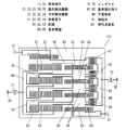
図1(a)は本発明の実施の形態1における弾性波装置101の回路図、図1(b)は弾性波装置101の断面模式図、図2は弾性波装置101のパターン図である。図1(a)、(b)、図2において、弾性波装置101は、圧電基板90の表面に、励振空間13を介して弾性波素子を封止する封止体14を有し、この封止体14の表面に信号端子11、12と基準電位端子81、82を有する。信号端子11と信号端子12は、それぞれ、弾性波装置101の入力端子と出力端子、または、出力端子と入力端子として用いられる。基準電位端子81、82はグランド端子として用いられ、2つの基準電位端子81、82は電気的に直接には接続されていない。圧電基板90上には、第1の配線61と第2の配線62と第3の配線63と第1の基準電極64と第2の基準電極65とを有する。第1の配線61は、信号端子11と信号端子12との間を接続する配線である。第1の配線61上には、一端子対弾性波素子からなる直列腕共振器21、22、23、24、25を直列に接続する。第2の配線62は、第1の配線61の上の接続点91、92、93、94と第1の基準電極64とを接続する複数の配線である。各第2の配線62上には、それぞれ、一端子対弾性波素子からなる並列腕共振器31、32、33、34が直列に接続される。直列腕共振器21、22、23、24、25および並列腕共振器31、32、33、34は、それぞれ、圧電基板90上に形成された一端子対弾性波素子であり、一対の反射器の間に挟まれた1個のIDT(Inter Digital Transduser)からなる。第3の配線63は、第1の配線61の上の接続点91、92、93、94と第2の基準電極65とを接続する複数の配線である。第3の配線63上には、それぞれ、櫛型電極からなる容量素子41、42、43、44を直列に接続する。ここで、容量素子41、42、43、44は、各々の容量の合計が2.05pFになるように設計している。第1の基準電極64は、封止体14を貫通する導体からなるインダクタ71を経由して基準電位端子81に接続される。第2の基準電極65は、封止体14を貫通する導体からなるインダクタ72を経由して基準電位端子82に接続される。第1の基準電極64と第2の基準電極65は、それぞれ、圧電基板90の互いに対向する端辺に配置し、互いに電気的に直接には接続しない。インダクタ71およびインダクタ72のインダクタンスは、0.10nH程度である。
(Embodiment 1)
1A is a circuit diagram of an acoustic wave device 101 according to Embodiment 1 of the present invention, FIG. 1B is a schematic cross-sectional view of the acoustic wave device 101, and FIG. 2 is a pattern diagram of the acoustic wave device 101. 1A, 1 </ b> B, and 2, an acoustic wave device 101 includes a sealing body 14 that seals an acoustic wave element through an excitation space 13 on the surface of a piezoelectric substrate 90. Signal terminals 11 and 12 and reference potential terminals 81 and 82 are provided on the surface of the stopper 14. The signal terminal 11 and the signal terminal 12 are used as an input terminal and an output terminal of the acoustic wave device 101 or as an output terminal and an input terminal, respectively. The reference potential terminals 81 and 82 are used as ground terminals, and the two reference potential terminals 81 and 82 are not electrically connected directly. On the piezoelectric substrate 90, a first wiring 61, a second wiring 62, a third wiring 63, a first reference electrode 64, and a second reference electrode 65 are provided. The first wiring 61 is a wiring that connects between the signal terminal 11 and the signal terminal 12. On the first wiring 61, series arm resonators 21, 22, 23, 24, and 25 composed of one-terminal-pair acoustic wave elements are connected in series. The second wiring 62 is a plurality of wirings that connect the connection points 91, 92, 93, 94 on the first wiring 61 and the first reference electrode 64. On each second wiring 62, parallel arm resonators 31, 32, 33, and 34 each consisting of a one-terminal pair acoustic wave element are connected in series. The series arm resonators 21, 22, 23, 24, 25 and the parallel arm resonators 31, 32, 33, 34 are respectively one-terminal-pair elastic wave elements formed on the piezoelectric substrate 90, and a pair of reflectors It consists of one IDT (Inter Digital Transducer) sandwiched between the two. The third wiring 63 is a plurality of wirings that connect the connection points 91, 92, 93, 94 on the first wiring 61 and the second reference electrode 65. On the third wiring 63, capacitive elements 41, 42, 43, and 44 each including a comb-shaped electrode are connected in series. Here, the capacitive elements 41, 42, 43, and 44 are designed so that the total of the respective capacitances is 2.05 pF. The first reference electrode 64 is connected to the reference potential terminal 81 via an inductor 71 made of a conductor that penetrates the sealing body 14. The second reference electrode 65 is connected to the reference potential terminal 82 via an inductor 72 made of a conductor that penetrates the sealing body 14. The first reference electrode 64 and the second reference electrode 65 are disposed on opposite sides of the piezoelectric substrate 90, respectively, and are not electrically connected directly to each other. The inductances of the inductor 71 and the inductor 72 are about 0.10 nH.

以上のように構成された弾性波装置101は、直列腕共振器21、22、23、24、25と並列腕共振器31、32、33、34によりラダー型フィルタを構成し、704MHz〜716MHzの送信帯域と734MHz〜746MHzの受信帯域を有するBand17の無線通信装置における共用器の送信フィルタとして設計したものであり、内蔵する圧電基板90と同等レベルの占有面積を有する極めて小型で低背のウエハレベル構造を実現したものである。   The elastic wave device 101 configured as described above includes a ladder-type filter including the series arm resonators 21, 22, 23, 24, and 25 and the parallel arm resonators 31, 32, 33, and 34, and operates at 704 MHz to 716 MHz. Designed as a transmission filter for a duplexer in a Band 17 wireless communication apparatus having a transmission band and a reception band of 734 MHz to 746 MHz, and an extremely small and low-profile wafer level having an occupation area equivalent to that of the built-in piezoelectric substrate 90 The structure is realized.

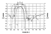
本発明の実施の形態1における弾性波装置101の電気特性を図3、図4に示す。図3、図4において、横軸は周波数、縦軸は減衰量であり、本発明の実施の形態1における弾性波装置101の電気特性Aを実線で示し、比較例の電気特性Eを破線で示す。図4において、通過帯域Sは送信帯域である704MHz〜716MHzであり、734MHz〜746MHzの受信帯域Tは、通過帯域Sの高域側の帯域外にある。   The electrical characteristics of the acoustic wave device 101 according to the first embodiment of the present invention are shown in FIGS. 3 and 4, the horizontal axis represents frequency, and the vertical axis represents attenuation. The electrical characteristic A of the acoustic wave device 101 according to the first embodiment of the present invention is indicated by a solid line, and the electrical characteristic E of the comparative example is indicated by a broken line. Show. In FIG. 4, the pass band S is 704 MHz to 716 MHz, which is a transmission band, and the reception band T of 734 MHz to 746 MHz is outside the band on the high frequency side of the pass band S.

図3、図4における比較例は、図13(a)、(b)に示した従来の弾性波装置100において、直列腕共振器121、122、123、124、125と並列腕共振器131、132、133、134のそれぞれを本発明の実施の形態1における弾性波装置101の直列腕共振器21、22、23、24、25と並列腕共振器31、32、33、34のそれぞれと同じ設計にして構成した704MHz〜716MHzの送信帯域を有するBand17の送信フィルタである。   3 and FIG. 4 show a series of arm resonators 121, 122, 123, 124, 125 and a parallel arm resonator 131 in the conventional acoustic wave device 100 shown in FIGS. 132, 133, and 134 are the same as the series arm resonators 21, 22, 23, 24, and 25 and the parallel arm resonators 31, 32, 33, and 34 of the acoustic wave device 101 according to the first embodiment of the present invention. This is a Band 17 transmission filter having a transmission band of 704 MHz to 716 MHz designed and configured.

図3より、本発明の実施の形態1における弾性波装置101の電気特性Aは、比較例の電気特性Eと比較して、1.3GHzより高い周波数領域において本発明の減衰特性が格段に優れていることがわかる。   As shown in FIG. 3, the electrical characteristic A of the acoustic wave device 101 according to the first embodiment of the present invention is significantly superior in the attenuation characteristic of the present invention in a frequency region higher than 1.3 GHz as compared with the electrical characteristic E of the comparative example. You can see that

比較例の減衰特性は、1.2GHz付近の減衰極E1と3GHz付近の減衰極E2が形成されているが、減衰極E1、E2間の幅が比較的狭く、3GHz付近からより高い周波数に行くに従って急激に減衰量が悪化している。   In the attenuation characteristic of the comparative example, an attenuation pole E1 near 1.2 GHz and an attenuation pole E2 near 3 GHz are formed, but the width between the attenuation poles E1 and E2 is relatively narrow, and the frequency goes from around 3 GHz to a higher frequency. As shown, the amount of attenuation suddenly deteriorates.

本発明の実施の形態1の弾性波装置101は、並列腕共振器31、32、33、34のそれぞれの静電容量の総和とインダクタ71による直列共振による2.3GHz近辺の減衰極A1が比較的広帯域かつ高減衰である。また図3より確認できるように高周波数領域(2.3GHz〜8.5GHz)において、良好な減衰特性が得られていることが判る。   The elastic wave device 101 according to the first embodiment of the present invention compares the total capacitance of the parallel arm resonators 31, 32, 33, and 34 with the attenuation pole A 1 near 2.3 GHz due to series resonance by the inductor 71. Wide bandwidth and high attenuation. Further, as can be seen from FIG. 3, it can be seen that good attenuation characteristics are obtained in the high frequency region (2.3 GHz to 8.5 GHz).

図4からは、本発明の実施の形態1の弾性波装置101の電気特性Aは、比較例の電気特性Eと比べて、通過帯域Sの高域側近傍の減衰量を良好に確保することができ、特に734MHz〜746MHzの受信帯域Tの減衰特性が優れていることがわかる。   From FIG. 4, the electrical characteristic A of the elastic wave device 101 according to the first embodiment of the present invention ensures a good attenuation in the vicinity of the high band side of the pass band S compared to the electrical characteristic E of the comparative example. In particular, it can be seen that the attenuation characteristic of the reception band T of 734 MHz to 746 MHz is excellent.

以上のように、本発明の実施の形態1の弾性波装置101は、容量素子41、42、43、44とインダクタ72を直列接続することでLCの直列共振によるなだらかな減衰極をGHz以上の高周波領域に形成することができるため、広帯域にわたって良好な減衰特性を得ることができた。   As described above, the elastic wave device 101 according to the first embodiment of the present invention connects the capacitive elements 41, 42, 43, 44 and the inductor 72 in series so that the gentle attenuation pole due to the LC series resonance is equal to or higher than GHz. Since it can be formed in a high frequency region, a good attenuation characteristic can be obtained over a wide band.

すなわち、容量素子41、42、43、44の各々の容量の合計を2.05pFとし、インダクタ72のインダクタンスを0.10nHとしたことにより、減衰極A1を11GHz近辺に形成することができ、非常に高い周波数領域まで良好な減衰特性を得ることができた。そして、容量素子41、42、43、44の容量値の合計とインダクタ72のインダクタンスを適切に設定することにより、減衰極の位置を調整することができる。   That is, by setting the total capacitance of the capacitive elements 41, 42, 43, and 44 to 2.05 pF and the inductance of the inductor 72 to 0.10 nH, the attenuation pole A1 can be formed in the vicinity of 11 GHz. Good attenuation characteristics were obtained up to a high frequency range. The position of the attenuation pole can be adjusted by appropriately setting the sum of the capacitance values of the capacitive elements 41, 42, 43, and 44 and the inductance of the inductor 72.

そして、本発明の実施の形態1の弾性波装置101は、容量素子41、42、43、44を圧電基板90上に形成し、圧電基板90上から基準電位端子81、82までを接続する導体レベルの非常に小さなインダクタンスでもって広帯域にわたる良好な減衰特性を得ることができるため、別途、インダクタを形成するための多層セラミック基板のような大掛かりな構造を必要とせずに、減衰特性の良好な弾性波装置を実現できるものであり、弾性波装置の小型化を実現できるものである。特に、ウエハレベルのように、セラミック基板等を有さない極めて小型の弾性波装置において良好な減衰特性を可能にする。   In the elastic wave device 101 according to the first embodiment of the present invention, the capacitive elements 41, 42, 43, and 44 are formed on the piezoelectric substrate 90, and the conductors connecting the piezoelectric substrate 90 to the reference potential terminals 81 and 82 are connected. Good damping characteristics over a wide band can be obtained with a very small inductance level, so there is no need for a large structure such as a multilayer ceramic substrate for forming an inductor separately. The wave device can be realized, and the elastic wave device can be miniaturized. In particular, it is possible to achieve good damping characteristics in an extremely small elastic wave device that does not have a ceramic substrate or the like as at the wafer level.

さらに、本発明の実施の形態1の弾性波装置101は、複数の並列腕共振器31、32、33、34を電気的に共通接続してインダクタ71を介して基準電位端子81に接続したことで、通過帯域の高域側近傍の減衰量を良好に確保することができ、特に734MHz〜746MHzの受信帯域の減衰量を良好にすることができた。   Furthermore, in the elastic wave device 101 according to the first embodiment of the present invention, the plurality of parallel arm resonators 31, 32, 33, and 34 are electrically connected in common and connected to the reference potential terminal 81 via the inductor 71. Thus, it was possible to secure a good attenuation in the vicinity of the high band side of the pass band, and in particular, it was possible to improve the attenuation in the reception band of 734 MHz to 746 MHz.

さらに、本発明の実施の形態1の弾性波装置101は、基準電位端子81と基準電位端子82を電気的に直接に接続しない構成にしたことで、容量素子41、42、43、44をローパスフィルタとして機能させることができるとともに、第1の基準電極64から第2の基準電極65への信号の回り込みを防止することができるため、減衰量を効果的に確保することができた。   Furthermore, the acoustic wave device 101 according to the first embodiment of the present invention has a configuration in which the reference potential terminal 81 and the reference potential terminal 82 are not directly electrically connected, so that the capacitive elements 41, 42, 43, and 44 are low-pass. In addition to being able to function as a filter, it is possible to prevent the signal from wrapping around from the first reference electrode 64 to the second reference electrode 65, so that the attenuation amount can be effectively ensured.

また、本発明の実施の形態1の弾性波装置101の構成は、回路的に見ると容量素子41は並列腕共振器31と実質的に並列接続されており、並列腕共振器31の反共振周波数を低周波側にシフトさせる作用を有するため、並列腕共振器31の共振周波数と反共振周波数の周波数差が実質的に小さくなる。同様に容量素子42は並列腕共振器32と並列接続されており、容量素子43は並列腕共振器33と並列接続されており、容量素子44は並列腕共振器34と並列接続されており、各々の共振器の共振周波数と反共振周波数の周波数差が実質的に小さくなる。したがって、より狭帯域のフィルタを作成することが可能であり、通過帯域が704MHz〜716MHzであるBand17の送信フィルタのように通過帯域幅/中心周波数で定義される比帯域が1.69%と比較的狭い帯域幅のフィルタを作成した場合、通過帯域近傍の減衰特性の良好なフィルタ特性が得られる。   Further, in the configuration of the acoustic wave device 101 according to the first embodiment of the present invention, the capacitance element 41 is substantially connected in parallel with the parallel arm resonator 31 in terms of a circuit, and the antiresonance of the parallel arm resonator 31 is achieved. Since it has the effect of shifting the frequency to the low frequency side, the frequency difference between the resonance frequency and antiresonance frequency of the parallel arm resonator 31 is substantially reduced. Similarly, the capacitive element 42 is connected in parallel with the parallel arm resonator 32, the capacitive element 43 is connected in parallel with the parallel arm resonator 33, and the capacitive element 44 is connected in parallel with the parallel arm resonator 34, The frequency difference between the resonance frequency and antiresonance frequency of each resonator is substantially reduced. Therefore, it is possible to create a narrower band filter, and the ratio band defined by the pass band width / center frequency is 1.69% compared to the Band 17 transmission filter whose pass band is 704 MHz to 716 MHz. When a filter with a narrow bandwidth is created, a filter characteristic having a good attenuation characteristic in the vicinity of the pass band can be obtained.

また、本発明の実施の形態1の弾性波装置101は、第1の基準電極64と第2の基準電極65を、それぞれ、圧電基板90の互いに対向する端辺に配置し、互いに電気的に直接には接続しないように構成することで、電磁界結合や、グランド配線を介した信号の伝達を抑制でき、良好な減衰特性が得られる。圧電基板90の表面上以外の部分であれば基準電位端子81と基準電位端子82が電気的に接続されていても本発明の効果を有するが、基準電位端子81と基準電位端子82が電気的に接続しない構成がより効果が大きい。   In the elastic wave device 101 according to the first embodiment of the present invention, the first reference electrode 64 and the second reference electrode 65 are arranged on opposite sides of the piezoelectric substrate 90, respectively, and electrically connected to each other. By configuring so as not to be directly connected, it is possible to suppress electromagnetic field coupling and signal transmission through the ground wiring, and to obtain good attenuation characteristics. Even if the reference potential terminal 81 and the reference potential terminal 82 are electrically connected to any part other than the surface of the piezoelectric substrate 90, the effect of the present invention is obtained. However, the reference potential terminal 81 and the reference potential terminal 82 are electrically connected. A configuration that does not connect to the device is more effective.

なお、本発明の実施の形態1における弾性波装置101は、704MHz〜716MHzの送信帯域を有するBand17の無線通信装置における送信フィルタであるが、本願発明は、他の通過帯域を有する高周波フィルタに適用してもよく、高周波フィルタを備えたデュプレクサのような装置に適用しても同様に効果を有し、1つの圧電基板の上に受信フィルタとともに設置する送信フィルタに適用しても良く、受信フィルタに適用しても良い。   The elastic wave device 101 according to the first embodiment of the present invention is a transmission filter in a Band 17 wireless communication device having a transmission band of 704 MHz to 716 MHz, but the present invention is applied to a high frequency filter having another pass band. Even if applied to a device such as a duplexer equipped with a high frequency filter, the same effect is obtained, and it may be applied to a transmission filter installed together with a reception filter on one piezoelectric substrate. You may apply to.

しかし、本願発明は、使用しようとする周波数帯域から大きく離れた周波数帯域における不要信号を広帯域に渡って抑制することができるため、特に、送信フィルタとして使用することにより、他の周波数帯域を使用する無線通信機器に対する妨害信号を抑制することができるという効果を有する。   However, according to the present invention, unnecessary signals in a frequency band far away from the frequency band to be used can be suppressed over a wide band. In particular, by using as a transmission filter, another frequency band is used. It has the effect that the interference signal with respect to a radio | wireless communication apparatus can be suppressed.

また、本発明の弾性波装置101では、全ての並列腕共振器に対して並列接続された容量素子を設けたが、少なくとも1つの並列腕共振器に対して並列接続された容量素子を有せば本願発明の効果を有する。しかし、十分な減衰量を確保するためには、できるだけ多くの並列腕共振器に容量素子を並列接続することが好ましく、全ての並列腕共振器に並列接続された容量素子を設けることがより好ましい。   In the acoustic wave device 101 of the present invention, the capacitive element connected in parallel to all the parallel arm resonators is provided, but the capacitive element connected in parallel to at least one parallel arm resonator should be provided. If it has the effect of this invention. However, in order to ensure a sufficient amount of attenuation, it is preferable to connect capacitive elements to as many parallel arm resonators as possible, and it is more preferable to provide capacitive elements connected in parallel to all the parallel arm resonators. .

また、本発明の実施の形態1の弾性波装置101では、インダクタ71およびインダクタ72は、封止体14を貫通する導体により構成したが、封止体14の中にスパイラル状やミアンダ状の配線を設けて使用しても良いものであり、屈曲部を有する導体により構成しても良い。   Further, in the elastic wave device 101 according to the first embodiment of the present invention, the inductor 71 and the inductor 72 are configured by conductors that penetrate the sealing body 14, but a spiral or meander-like wiring is formed in the sealing body 14. May be used, and may be formed of a conductor having a bent portion.

また、本発明の実施の形態1の弾性波装置101では、全ての並列腕共振器31、32、33、34を1つの基準電極64に接続して第1の基準電位端子81に接続したが、並列腕共振器に接続する基準電極を複数に分けても良い。   In the elastic wave device 101 according to the first embodiment of the present invention, all the parallel arm resonators 31, 32, 33, and 34 are connected to one reference electrode 64 and connected to the first reference potential terminal 81. The reference electrode connected to the parallel arm resonator may be divided into a plurality of parts.

図5は、本発明の実施の形態1の他の弾性波装置102の回路図であり、図1、図2で示した本発明の実施の形態1における弾性波装置101と同じ構成要素については同一番号を付しており、その説明は省略する。図5に示す実施の形態1の他の弾性波装置102が、本発明の実施の形態1の弾性波装置101と異なる点は、並列腕共振器31、32、33、34に接続される基準電極とインダクタと基準電位端子を2つに分けたことである。すなわち、並列腕共振器31は、基準電極66とインダクタ73を介して基準電位端子83に接続し、並列腕共振器32、33、34は、基準電極67とインダクタ74を介して基準電位端子84に接続したものである。   FIG. 5 is a circuit diagram of another elastic wave device 102 according to the first embodiment of the present invention. The same components as those of the elastic wave device 101 according to the first embodiment of the present invention shown in FIGS. The same number is given and the explanation is omitted. The other elastic wave device 102 of the first embodiment shown in FIG. 5 is different from the elastic wave device 101 of the first embodiment of the present invention in that the reference connected to the parallel arm resonators 31, 32, 33, and 34 is used. That is, the electrode, the inductor, and the reference potential terminal are divided into two. That is, the parallel arm resonator 31 is connected to the reference potential terminal 83 via the reference electrode 66 and the inductor 73, and the parallel arm resonators 32, 33, and 34 are connected to the reference potential terminal 84 via the reference electrode 67 and the inductor 74. Is connected to.

図5に示す実施の形態1の他の弾性波装置102の電気特性を図6に示す。   FIG. 6 shows the electrical characteristics of another elastic wave device 102 of the first embodiment shown in FIG.

図6において、横軸は周波数、縦軸は減衰量であり、本発明の実施の形態1における他の弾性波装置102の電気特性Bを一点破線で示し、比較例の電気特性Eを破線で示し、本発明の実施の形態1における弾性波装置101の電気特性Aを実線で示す。   In FIG. 6, the horizontal axis represents frequency, and the vertical axis represents attenuation. The electric characteristic B of another elastic wave device 102 according to Embodiment 1 of the present invention is indicated by a one-dot broken line, and the electric characteristic E of the comparative example is indicated by a broken line. The electrical characteristic A of the acoustic wave device 101 according to the first embodiment of the present invention is indicated by a solid line.

図6において、通過帯域Sである送信帯域は704MHz〜716MHzであり、通過帯域外である受信帯域Tは734MHz〜746MHzである。   In FIG. 6, the transmission band that is the pass band S is 704 MHz to 716 MHz, and the reception band T that is outside the pass band is 734 MHz to 746 MHz.

このような構成とすることで、実施の形態1の他の弾性波装置102は通過帯域低域側の減衰特性を改善することができた。   By adopting such a configuration, the other acoustic wave device 102 of the first embodiment was able to improve the attenuation characteristics on the low pass band side.

(実施の形態2)
図7は本発明の実施の形態2における弾性波装置103を示す回路図、図8は同弾性波装置103のパターン図であり、図1、図2で示した本発明の実施の形態1における弾性波装置101と同じ構成要素については同一番号を付しており、その説明は省略する。
(Embodiment 2)
FIG. 7 is a circuit diagram showing the acoustic wave device 103 according to the second embodiment of the present invention, and FIG. 8 is a pattern diagram of the acoustic wave device 103 according to the first embodiment of the present invention shown in FIGS. The same components as those of the elastic wave device 101 are denoted by the same reference numerals, and the description thereof is omitted.

本発明の実施の形態2おける弾性波装置103が、本発明の実施の形態1における弾性波装置101と異なる点は、並列腕共振器31、32、33、34に並列に容量素子45、46、47、48を接続するとともに、第3の配線63に接続した容量素子41、42、43、44の替わりに、第3の配線63に静電容量の異なる容量素子51、52、53、54を接続したことである。   The elastic wave device 103 according to the second embodiment of the present invention is different from the elastic wave device 101 according to the first embodiment of the present invention in that the capacitive elements 45 and 46 are parallel to the parallel arm resonators 31, 32, 33 and 34. , 47, and 48, and instead of the capacitive elements 41, 42, 43, and 44 connected to the third wiring 63, capacitive elements 51, 52, 53, and 54 having different capacitances are connected to the third wiring 63. Is connected.

なお、本発明の実施の形態2の弾性波装置103における、直列腕共振器21、22、23、24、25と、並列腕共振器31、32、33、34の各設計数値は、本発明の実施の形態1の弾性波装置101のものと同じ構成のものである。   In the elastic wave device 103 according to the second embodiment of the present invention, the design numerical values of the series arm resonators 21, 22, 23, 24, and 25 and the parallel arm resonators 31, 32, 33, and 34 are as follows. The configuration is the same as that of the elastic wave device 101 of the first embodiment.

そして、実施の形態2の弾性波装置103における容量素子51の容量と容量素子45の容量の合計を実施の形態1の弾性波装置101における容量素子41の容量と等しく設計し、実施の形態2の弾性波装置103における容量素子52の容量と容量素子46の容量の合計を実施の形態1の弾性波装置101における容量素子42の容量と等しく設計し、実施の形態2の弾性波装置103における容量素子53の容量と容量素子47の容量の合計を実施の形態1の弾性波装置101における容量素子43の容量と等しく設計し、実施の形態2の弾性波装置103における容量素子54の容量と容量素子48の容量の合計を実施の形態1の弾性波装置101における容量素子44の容量と等しく設計した。   Then, the total of the capacitance of the capacitive element 51 and the capacitance of the capacitive element 45 in the acoustic wave device 103 according to the second embodiment is designed to be equal to the capacitance of the capacitive element 41 in the acoustic wave device 101 according to the first embodiment. The total of the capacitance of the capacitive element 52 and the capacitance of the capacitive element 46 in the elastic wave device 103 is designed to be equal to the capacitance of the capacitive element 42 in the elastic wave device 101 of the first embodiment, and in the elastic wave device 103 of the second embodiment. The sum of the capacitance of the capacitive element 53 and the capacitance of the capacitive element 47 is designed to be equal to the capacitance of the capacitive element 43 in the acoustic wave device 101 of the first embodiment, and the capacitance of the capacitive element 54 in the acoustic wave device 103 of the second embodiment is The total capacity of the capacitive element 48 is designed to be equal to the capacity of the capacitive element 44 in the acoustic wave device 101 of the first embodiment.

本発明の実施の形態2においては、例えば並列腕共振器31を例に説明すると、回路的に見て容量素子51と容量素子45は、ともに並列腕共振器31に並列接続されており、容量素子51と容量素子45の容量の合計を一定にした条件下で、容量素子51の容量と容量素子45の容量の比率を適宜設定することにより、通過帯域幅などの特性に影響を与えることなく、高周波領域の減衰特性が改善できる。他の並列腕共振器32、33、34についても同様に機能するため、実施の形態1と同じ通過帯域特性を保った状態で、減衰特性を改善でき、減衰特性の設計自由度が向上する。   In Embodiment 2 of the present invention, for example, the parallel arm resonator 31 will be described as an example. The capacitive element 51 and the capacitive element 45 are both connected in parallel to the parallel arm resonator 31 in terms of a circuit, and the capacitance By appropriately setting the ratio of the capacitance of the capacitive element 51 and the capacitance of the capacitive element 45 under the condition that the total capacitance of the element 51 and the capacitive element 45 is constant, the characteristics such as the pass bandwidth are not affected. The attenuation characteristic in the high frequency region can be improved. Since the other parallel arm resonators 32, 33, and 34 function in the same manner, the attenuation characteristic can be improved while maintaining the same passband characteristic as in the first embodiment, and the degree of freedom in designing the attenuation characteristic is improved.

次に、本発明の実施の形態2における弾性波装置103の電気特性を図9、図10に示す。   Next, the electrical characteristics of the acoustic wave device 103 according to Embodiment 2 of the present invention are shown in FIGS.

図9、図10において、横軸は周波数、縦軸は減衰量であり、本発明の実施の形態2における弾性波装置103の電気特性Cを実線で示し、本発明の実施の形態1における弾性波装置101の電気特性Aを二点破線で示し、実施の形態1で説明した比較例の電気特性Eを破線で示す。図9、図10において、通過帯域Sは送信帯域である704MHz〜716MHzであり、734MHz〜746MHzの受信帯域Tは、通過帯域Sの高域側の帯域外にある。   9 and 10, the horizontal axis represents frequency and the vertical axis represents attenuation, and the electric characteristic C of the acoustic wave device 103 according to the second embodiment of the present invention is indicated by a solid line, and the elasticity according to the first embodiment of the present invention is illustrated. The electric characteristic A of the wave device 101 is indicated by a two-dot broken line, and the electric characteristic E of the comparative example described in the first embodiment is indicated by a broken line. 9 and 10, the pass band S is 704 MHz to 716 MHz, which is a transmission band, and the reception band T of 734 MHz to 746 MHz is outside the high band side of the pass band S.

図9および図10に示すように、本発明の実施の形態2の弾性波装置103の電気特性Cは、1.4GHz〜3.7GHzの領域で2つの減衰極C1、C2を有し、実施の形態1の弾性波装置101の電気特性Aと異なる位置に2つの減衰極を設けることができた。このように本発明の実施の形態2の弾性波装置103は、通過帯域特性に影響を与えることなく減衰極を追加するとともに所望の周波数に設定することが可能になり、良好な減衰特性を実現できる。   As shown in FIGS. 9 and 10, the electrical characteristic C of the elastic wave device 103 according to the second embodiment of the present invention has two attenuation poles C1 and C2 in the region of 1.4 GHz to 3.7 GHz. It was possible to provide two attenuation poles at positions different from the electrical characteristics A of the elastic wave device 101 of the first embodiment. As described above, the elastic wave device 103 according to the second embodiment of the present invention can add an attenuation pole without affecting the passband characteristics and can set a desired frequency, thereby realizing a good attenuation characteristic. it can.

なお、本発明の実施の形態2における弾性波装置103では、全ての並列腕共振器に回路的に見て2つの容量素子が接続された例を示したが、全ての並列腕共振器に2つの容量素子が接続する必要はなく、並列腕共振器と容量素子が回路的に並列接続となっていない並列腕共振器や並列腕共振器に1つの容量素子が接続される並列腕共振器を有してもよい。   In the elastic wave device 103 according to the second embodiment of the present invention, an example is shown in which two capacitive elements are connected to all parallel arm resonators in terms of a circuit. There is no need to connect two capacitive elements, a parallel arm resonator in which the parallel arm resonator and the capacitive element are not connected in parallel in a circuit, or a parallel arm resonator in which one capacitive element is connected to the parallel arm resonator. You may have.

(実施の形態3)
図11は本発明の実施の形態3における弾性波装置104を示す回路図であり、図7、図8で示した本発明の実施の形態2における弾性波装置103と同じ構成要素については同一番号を付しており、その説明は省略する。
(Embodiment 3)
FIG. 11 is a circuit diagram showing acoustic wave device 104 according to Embodiment 3 of the present invention. The same components as those of acoustic wave device 103 according to Embodiment 2 of the present invention shown in FIGS. The description is omitted.

本発明の実施の形態3における弾性波装置104が、本発明の実施の形態2における弾性波装置103と異なる点は、直列腕共振器21、22、23、24、25の中で、信号端子11に最も近い直列腕共振器21に並列に容量素子49を設けるとともに、信号端子12に最も近い直列腕共振器25に並列に容量素子50を設けたことである。   The elastic wave device 104 according to the third embodiment of the present invention is different from the elastic wave device 103 according to the second embodiment of the present invention in the series arm resonators 21, 22, 23, 24, and 25, with signal terminals. The capacitive element 49 is provided in parallel to the series arm resonator 21 closest to 11, and the capacitive element 50 is provided in parallel to the series arm resonator 25 closest to the signal terminal 12.

なお、本発明の実施の形態3の弾性波装置104における、直列腕共振器21、22、23、24、25と、並列腕共振器31、32、33、34と、容量素子51、52、53、54、45、46、47、48の各設計数値は、本発明の実施の形態2の弾性波装置103におけるものと同じである。   In the elastic wave device 104 according to the third embodiment of the present invention, the series arm resonators 21, 22, 23, 24, 25, the parallel arm resonators 31, 32, 33, 34, and the capacitive elements 51, 52, The design values of 53, 54, 45, 46, 47, and 48 are the same as those in the acoustic wave device 103 according to the second embodiment of the present invention.

本発明の実施の形態3における弾性波装置104の電気特性を図12に示す。図12において、横軸は周波数、縦軸は減衰量であり、本発明の実施の形態における弾性波装置10の電気特性Dを実線で示し、本発明の実施の形態1における弾性波装置101の電気特性Aを一点破線で示し、本発明の実施の形態1で説明した比較例の電気特性Eを破線で示す。図12において、通過帯域Sは送信帯域である704MHz〜716MHzであり、734MHz〜746MHzの受信帯域Tは、通過帯域Sの高域側の帯域外にある。
FIG. 12 shows the electrical characteristics of the acoustic wave device 104 according to Embodiment 3 of the present invention. 12, the horizontal axis represents frequency and the vertical axis is attenuation, showing the electrical characteristics D of the acoustic wave device 104 according to the third embodiment of the present invention in solid lines, acoustic wave device according to the first embodiment of the present invention An electric characteristic A of 101 is indicated by a one-dot broken line, and an electric characteristic E of the comparative example described in the first embodiment of the present invention is indicated by a broken line. In FIG. 12, the pass band S is 704 MHz to 716 MHz, which is a transmission band, and the reception band T of 734 MHz to 746 MHz is outside the high band side band of the pass band S.

図12に示すように、本発明の実施の形態における弾性波装置10の電気特性Dは、本発明の実施の形態1における弾性波装置101の電気特性Aに近い特性を有する領域もあるが、通過帯域Sの高域部において挿入損失をより低減することができた。
As shown in FIG. 12, the electrical characteristics D of the acoustic wave device 104 according to the third embodiment of the present invention, there is also a region having characteristics similar to the electrical characteristics A of the acoustic wave device 101 according to the first embodiment of the present invention However, the insertion loss can be further reduced in the high band part of the pass band S.

以上のように、本発明の実施の形態3における弾性波装置104は、信号端子11、12に最も近い直列腕共振器21、25に並列接続された容量素子49、50を設けることで、狭帯域なフィルタを形成した際のインピーダンスマッチングがよくなり、インピーダンスミスマッチによる損失が小さくなり、低損失な弾性波装置が得られる。   As described above, the elastic wave device 104 according to the third embodiment of the present invention is narrow by providing the capacitive elements 49 and 50 connected in parallel to the series arm resonators 21 and 25 closest to the signal terminals 11 and 12. Impedance matching is improved when a band-pass filter is formed, loss due to impedance mismatch is reduced, and a low-loss acoustic wave device can be obtained.

なお、実施の形態1、実施の形態2および実施の形態3の弾性波装置に用いられる容量素子は必ずしも櫛電極により構成形成される必要はなく、2枚の平行平板で誘電体を挟むように形成されてもよい。   Note that the capacitive element used in the elastic wave devices of the first, second, and third embodiments is not necessarily formed by the comb electrode, and the dielectric is sandwiched between two parallel plates. It may be formed.

また、実施の形態1、実施の形態2および実施の形態3の弾性波装置に用いられる弾性波素子は弾性表面波、境界波、バルク波の内、いずれかを用いたものでもよい。   The elastic wave element used in the elastic wave devices of the first embodiment, the second embodiment, and the third embodiment may use any one of a surface acoustic wave, a boundary wave, and a bulk wave.

本発明に係る弾性波装置は、低挿入損失かつ高周波数領域においても良好な通過帯域外減衰量を有するという優れた効果を奏するものであり、主として移動体通信機器にフィルタやアンテナ共用器として用いられる弾性波装置において有用となるものである。   The elastic wave device according to the present invention has an excellent effect of having a low insertion loss and a good out-of-pass attenuation even in a high frequency region, and is mainly used as a filter or an antenna duplexer in a mobile communication device. This is useful in an elastic wave device.

11、12 信号端子
21、22、23、24、25 直列腕共振器
31、32、33、34 並列腕共振器
41、42、43、44、45、46、47、48、49、50、51、52、53、54 容量素子
61 第1の配線
62 第2の配線
63 第3の配線
64 第1の基準電極
65 第2の基準電極
71、72、73、74 インダクタ
81、82、83、84 基準電位端子
90 圧電基板
91、92、93、94 接続点
101、102、103、104 弾性波装置
11, 12 Signal terminal 21, 22, 23, 24, 25 Series arm resonator 31, 32, 33, 34 Parallel arm resonator 41, 42, 43, 44, 45, 46, 47, 48, 49, 50, 51 , 52, 53, 54 Capacitor element 61 First wiring 62 Second wiring 63 Third wiring 64 First reference electrode 65 Second reference electrode 71, 72, 73, 74 Inductors 81, 82, 83, 84 Reference potential terminal 90 Piezoelectric substrate 91, 92, 93, 94 Connection point 101, 102, 103, 104 Elastic wave device

Claims (20)

2つの信号端子の間に接続され、圧電基板の表面に形成された第1の配線と、
前記第1の配線に直列に接続され、一端子対弾性波素子を含む直列腕共振器と、
第1の基準電位端子に第1のインダクタを介して接続され、前記圧電基板の表面に形成された第1の基準電極と、
前記第1の配線上に設けられた接続点と前記第1の基準電極との間に接続された第2の配線と、
前記第2の配線に直列に接続され、一端子対弾性波素子を含む並列腕共振器と
を備え、
第2の基準電位端子に第2のインダクタを介して接続され、前記圧電基板の表面において前記第1の基準電極から電気的に分離された第2の基準電極を設け、
前記第2の基準電極と前記接続点とを接続する第3の配線を設け、
前記第3の配線に第1の容量素子が直列接続され、
前記第1の容量素子は前記第2の基準電極を介して前記第1のインダクタに直列接続される弾性波装置。
A first wiring connected between the two signal terminals and formed on the surface of the piezoelectric substrate;
A series arm resonator connected in series to the first wiring and including a one-terminal acoustic wave element;
A first reference electrode connected to a first reference potential terminal via a first inductor and formed on the surface of the piezoelectric substrate;
A second wiring connected between a connection point provided on the first wiring and the first reference electrode;
A parallel arm resonator connected in series to the second wiring and including a one-terminal acoustic wave element;
A second reference electrode connected to a second reference potential terminal via a second inductor and electrically separated from the first reference electrode on the surface of the piezoelectric substrate;
Providing a third wiring connecting the second reference electrode and the connection point;
A first capacitive element is connected in series to the third wiring ,
The first capacitive element is an acoustic wave device connected in series to the first inductor via the second reference electrode .
前記第1の基準電極を前記圧電基板の表面の第1の端辺の側に形成し、
前記第2の基準電極を前記圧電基板の表面の第1の端辺と対向する第2の端辺の側に形成した請求項1記載の弾性波装置。
Forming the first reference electrode on the first end side of the surface of the piezoelectric substrate;
The acoustic wave device according to claim 1, wherein the second reference electrode is formed on a second end side facing the first end side of the surface of the piezoelectric substrate.
前記第1の基準電位端子と前記第2の基準電位端子とを、同一の電位を有する基準電位端子として形成する請求項1又は2に記載の弾性波装置。 3. The acoustic wave device according to claim 1, wherein the first reference potential terminal and the second reference potential terminal are formed as reference potential terminals having the same potential. 前記同一の電位はグランド電位である請求項3記載の弾性波装置。 4. The acoustic wave device according to claim 3, wherein the same potential is a ground potential. 前記並列腕共振器に並列に第2の容量素子を接続した請求項1乃至4のいずれか一項記載の弾性波装置。 The elastic wave device according to claim 1, wherein a second capacitive element is connected in parallel to the parallel arm resonator. 前記直列腕共振器を複数備え、前記直列腕共振器のうち、他の直列腕共振器を介さずに前記信号端子の一方に接続された直列腕共振器に、第3の容量素子が並列接続されている請求項1乃至5のいずれか一項記載の弾性波装置。 A plurality of the series arm resonators are provided, and a third capacitor element is connected in parallel to the series arm resonator connected to one of the signal terminals without passing through another series arm resonator among the series arm resonators. acoustic wave apparatus according to any one claim of Motomeko 1 to 5 that have been. 前記弾性波装置の占有面積は前記圧電基板の占有面積とほぼ等しい請求項1記載の弾性波装置。 The elastic wave device according to claim 1, wherein an occupied area of the elastic wave device is substantially equal to an occupied area of the piezoelectric substrate. 前記第1の容量素子は2枚の平行平板で誘電体を挟むように構成される請求項1記載の弾性波装置。 The elastic wave device according to claim 1, wherein the first capacitive element is configured to sandwich a dielectric between two parallel flat plates. 前記第1の容量素子は櫛型電極を含む請求項1記載の弾性波装置。 The elastic wave device according to claim 1, wherein the first capacitive element includes a comb-shaped electrode. 前記第1の容量素子は複数の容量素子を含む請求項1記載の弾性波装置。The acoustic wave device according to claim 1, wherein the first capacitive element includes a plurality of capacitive elements. 前記複数の容量素子それぞれが、前記第2の基準電極を介して前記第1のインダクタに直列接続される請求項10記載の弾性波装置。The acoustic wave device according to claim 10, wherein each of the plurality of capacitive elements is connected in series to the first inductor via the second reference electrode. 前記第1のインダクタは1つのインダクタとして構成される請求項1乃至11のいずれか一項記載の弾性波装置。The acoustic wave device according to any one of claims 1 to 11, wherein the first inductor is configured as one inductor. 前記第2のインダクタは1つのインダクタとして構成される請求項1乃至12のいずれか一項記載の弾性波装置。The acoustic wave device according to claim 1, wherein the second inductor is configured as a single inductor. 前記直列腕共振器と前記並列腕共振器とはラダー型フィルタを形成する請求項1記載の弾性波装置。 The acoustic wave device according to claim 1, wherein the series arm resonator and the parallel arm resonator form a ladder type filter. 前記圧電基板の表面に、励振空間を介して前記直列腕共振器及び前記並列腕共振器を封止する封止体をさらに含む請求項1記載の弾性波装置。 The acoustic wave device according to claim 1, further comprising a sealing body that seals the series arm resonator and the parallel arm resonator through an excitation space on a surface of the piezoelectric substrate. 前記第1のインダクタ及び前記第2のインダクタの少なくとも一方は、前記封止体を貫通する導体を含む請求項15記載の弾性波装置。 Wherein at least one of the first inductor and the second inductor, the elastic wave device including請 Motomeko 15 wherein the conductor extending through the sealing body. 前記第の基準電極が複数の基準電極部分に分割される請求項1記載の弾性波装置。 The acoustic wave device according to claim 1 , wherein the first reference electrode is divided into a plurality of reference electrode portions. 前記並列腕共振器を複数備え、前記並列腕共振器の1つが前記基準電極部分の1つに接続される請求項17記載の弾性波装置。 The elastic wave device according to claim 17 , comprising a plurality of the parallel arm resonators, wherein one of the parallel arm resonators is connected to one of the reference electrode portions. 前記1つ以外の前記並列腕共振器が前記1つ以外の前記基準電極部分に接続される請求項18記載の弾性波装置。 The elastic wave device according to claim 18 , wherein the parallel arm resonators other than the one are connected to the reference electrode portions other than the one. 弾性表面波、弾性境界波、及びバルク波のいずれか1つが用いられる請求項1乃至19のいずれか一項記載の弾性波装置。 The elastic wave device according to any one of claims 1 to 19 , wherein any one of a surface acoustic wave, a boundary acoustic wave, and a bulk wave is used.
JP2012116192A 2012-05-22 2012-05-22 Elastic wave device Active JP5955095B2 (en)

Priority Applications (1)

Application Number Priority Date Filing Date Title
JP2012116192A JP5955095B2 (en) 2012-05-22 2012-05-22 Elastic wave device

Applications Claiming Priority (1)

Application Number Priority Date Filing Date Title
JP2012116192A JP5955095B2 (en) 2012-05-22 2012-05-22 Elastic wave device

Publications (3)

Publication Number Publication Date
JP2013243570A JP2013243570A (en) 2013-12-05
JP2013243570A5 JP2013243570A5 (en) 2015-04-30
JP5955095B2 true JP5955095B2 (en) 2016-07-20

Family

ID=49844038

Family Applications (1)

Application Number Title Priority Date Filing Date
JP2012116192A Active JP5955095B2 (en) 2012-05-22 2012-05-22 Elastic wave device

Country Status (1)

Country Link
JP (1) JP5955095B2 (en)

Families Citing this family (3)

* Cited by examiner, † Cited by third party
Publication number Priority date Publication date Assignee Title
WO2015119178A1 (en) 2014-02-10 2015-08-13 株式会社村田製作所 Variable filter circuit and wireless communication device
US9608595B1 (en) * 2015-11-13 2017-03-28 Resonant Inc. Acoustic wave filter with enhanced rejection
US10305447B2 (en) 2015-11-13 2019-05-28 Resonant Inc. Acoustic wave filter with enhanced rejection

Family Cites Families (11)

* Cited by examiner, † Cited by third party
Publication number Priority date Publication date Assignee Title
JP3201017B2 (en) * 1992-11-13 2001-08-20 株式会社村田製作所 Ladder type surface acoustic wave filter
JPH09167937A (en) * 1995-12-18 1997-06-24 Oki Electric Ind Co Ltd Surface acoustic wave filter
JP3380417B2 (en) * 1997-02-12 2003-02-24 沖電気工業株式会社 Polarized surface acoustic wave filter
DE19932649A1 (en) * 1999-07-13 2001-02-08 Epcos Ag Reactance filter type SAW filter with improved stop band suppression and method for optimizing the stop band suppression
JP4382945B2 (en) * 2000-01-31 2009-12-16 京セラ株式会社 Surface acoustic wave device
JP3827232B2 (en) * 2003-05-13 2006-09-27 Tdk株式会社 Filter device and duplexer using the same
JP2005033246A (en) * 2003-07-07 2005-02-03 Matsushita Electric Ind Co Ltd Saw filter and electronic device using the same
JP2005093465A (en) * 2003-09-12 2005-04-07 Murata Mfg Co Ltd Thin film capacitor, piezoelectric filter and its manufacturing process, demultiplexer, and communication device
WO2008018452A1 (en) * 2006-08-07 2008-02-14 Kyocera Corporation Method for manufacturing surface acoustic wave device
JP4894927B2 (en) * 2008-06-16 2012-03-14 株式会社村田製作所 Boundary acoustic wave device
JP2010011300A (en) * 2008-06-30 2010-01-14 Murata Mfg Co Ltd Resonator device, filter including the same, and duplexer

Also Published As

Publication number Publication date
JP2013243570A (en) 2013-12-05

Similar Documents

Publication Publication Date Title
US9998098B2 (en) Band pass filter and duplexer
US9503051B2 (en) High-frequency module having a matching element coupled to a connection unit
JP5081742B2 (en) Antenna duplexer
KR100280611B1 (en) Surface acoustic wave device
US20150054597A1 (en) Elastic wave filter device and duplexer
EP1783901B1 (en) Surface acoustic wave device
JPWO2011061904A1 (en) Elastic wave filter device and antenna duplexer using the same
US10715108B2 (en) Filter device and multiplexer
KR102312071B1 (en) Multiplexer
US20140176257A1 (en) Elastic-wave filter device
US11115001B2 (en) Receiving filter, multiplexer, and communication apparatus
JP5185057B2 (en) Duplexer
US10666229B2 (en) Duplexer
WO2007066608A1 (en) Composite filter
JP5782015B2 (en) Electronic components
JP5955095B2 (en) Elastic wave device
JP2021016116A (en) Multiplexer
JPWO2006040923A1 (en) Duplexer
JP2014033377A (en) Antenna duplexer
US11323098B2 (en) Duplexer
US11444597B2 (en) Acoustic wave filter device
US11362642B2 (en) Acoustic wave filter device, composite filter device, and multiplexer
JP5673897B2 (en) Elastic wave device and demultiplexing device
CN109314504B (en) Elastic wave filter device
US11405018B2 (en) Filter and multiplexer

Legal Events

Date Code Title Description
A711 Notification of change in applicant

Free format text: JAPANESE INTERMEDIATE CODE: A712

Effective date: 20141128

A521 Request for written amendment filed

Free format text: JAPANESE INTERMEDIATE CODE: A523

Effective date: 20150317

A621 Written request for application examination

Free format text: JAPANESE INTERMEDIATE CODE: A621

Effective date: 20150317

A977 Report on retrieval

Free format text: JAPANESE INTERMEDIATE CODE: A971007

Effective date: 20160215

A131 Notification of reasons for refusal

Free format text: JAPANESE INTERMEDIATE CODE: A131

Effective date: 20160223

A521 Request for written amendment filed

Free format text: JAPANESE INTERMEDIATE CODE: A523

Effective date: 20160331

TRDD Decision of grant or rejection written
A01 Written decision to grant a patent or to grant a registration (utility model)

Free format text: JAPANESE INTERMEDIATE CODE: A01

Effective date: 20160517

A61 First payment of annual fees (during grant procedure)

Free format text: JAPANESE INTERMEDIATE CODE: A61

Effective date: 20160614

R150 Certificate of patent or registration of utility model

Ref document number: 5955095

Country of ref document: JP

Free format text: JAPANESE INTERMEDIATE CODE: R150

S533 Written request for registration of change of name

Free format text: JAPANESE INTERMEDIATE CODE: R313533

R350 Written notification of registration of transfer

Free format text: JAPANESE INTERMEDIATE CODE: R350

R250 Receipt of annual fees

Free format text: JAPANESE INTERMEDIATE CODE: R250

R250 Receipt of annual fees

Free format text: JAPANESE INTERMEDIATE CODE: R250

R250 Receipt of annual fees

Free format text: JAPANESE INTERMEDIATE CODE: R250

R250 Receipt of annual fees

Free format text: JAPANESE INTERMEDIATE CODE: R250

R250 Receipt of annual fees

Free format text: JAPANESE INTERMEDIATE CODE: R250