JP5950552B2 - IMAGING DEVICE AND IMAGING DEVICE CONTROL METHOD - Google Patents
IMAGING DEVICE AND IMAGING DEVICE CONTROL METHOD Download PDFInfo
- Publication number
- JP5950552B2 JP5950552B2 JP2011261751A JP2011261751A JP5950552B2 JP 5950552 B2 JP5950552 B2 JP 5950552B2 JP 2011261751 A JP2011261751 A JP 2011261751A JP 2011261751 A JP2011261751 A JP 2011261751A JP 5950552 B2 JP5950552 B2 JP 5950552B2
- Authority
- JP
- Japan
- Prior art keywords
- image
- light
- dark current
- correction
- shading correction
- Prior art date
- Legal status (The legal status is an assumption and is not a legal conclusion. Google has not performed a legal analysis and makes no representation as to the accuracy of the status listed.)
- Expired - Fee Related
Links
Images


Landscapes
- Transforming Light Signals Into Electric Signals (AREA)
Description
本発明は撮像装置、及び撮像装置の制御方法に関し、特に、輝度シェーディング補正による画像周辺部の画像品質の低下度合い及び低下頻度を軽減する技術に関する。 The present invention relates to an imaging apparatus and a method for controlling the imaging apparatus , and more particularly to a technique for reducing the degree and frequency of image quality degradation at the periphery of an image due to luminance shading correction.
デジタルスチルカメラやデジタルビデオカメラ等の撮像装置においては、撮像素子として主にCCDやCMOSが使用されている。これら撮像素子では、温度と蓄積時間に依存する暗電流が、温度が8℃から10℃で約2倍に増加し、蓄積時間に比例して増加することが知られている。そのため、撮像素子が受光していない場合でも、暗電流によるムラや固定パターン(以下「暗電流ムラ」という)が発生することがある。また、撮像素子周辺の回路が発熱、発光する場合があり、このような発熱、発光によって撮像素子の有効画素部(記録画素領域)の周辺に局所的な暗電流ムラが発生する場合がある。 In an imaging apparatus such as a digital still camera or a digital video camera, a CCD or a CMOS is mainly used as an imaging element. In these imaging devices, it is known that the dark current depending on the temperature and the accumulation time increases approximately twice as the temperature increases from 8 ° C. to 10 ° C., and increases in proportion to the accumulation time. Therefore, even when the image sensor is not receiving light, unevenness due to dark current or a fixed pattern (hereinafter referred to as “dark current unevenness”) may occur. In addition, a circuit around the image sensor may generate heat and emit light, and such heat generation and light emission may cause local dark current unevenness around the effective pixel portion (recording pixel region) of the image sensor.
図12は、暗電流ムラの一例を模式的示す図である。撮像素子の有効画素部において、領域Aは周辺回路部が発光することにより発生した暗電流ムラを示しており、領域Bは垂直転送路暗電流が高温時に有効画素部右側で顕著に発生したことに起因する暗電流ムラを示している。 FIG. 12 is a diagram schematically illustrating an example of dark current unevenness. In the effective pixel portion of the image sensor, the region A shows dark current unevenness generated by the peripheral circuit portion emitting light, and the region B is that the vertical transfer path dark current is remarkably generated on the right side of the effective pixel portion at a high temperature. It shows dark current unevenness caused by.
ところで、撮像装置では、撮影された画像周辺部の光量が低下する現象、いわゆる輝度シェーディングが発生することも知られている。撮像装置の外部から光を入力する撮像レンズ等の特性が原因となって、撮影された画像に輝度のムラが生じる場合がある。例えば、白一色の均一な被写体を所定の光学機器で撮影して得られた画像について考える。この場合、理想的な撮像装置であれば、画像の全域が均一な白色となるはずである。しかし、実際には、画像の一部が他の部分よりも明るかったり暗かったりする場合がある。このような輝度のムラを、以降、「輝度シェーディング」と記す。 By the way, it is also known that a phenomenon in which the amount of light at the periphery of a captured image is reduced, that is, so-called luminance shading occurs in the imaging apparatus. Due to the characteristics of an imaging lens that inputs light from the outside of the imaging device, uneven brightness may occur in the captured image. For example, consider an image obtained by photographing a uniform subject of white color with a predetermined optical device. In this case, if it is an ideal imaging device, the whole area of the image should be uniform white. However, in practice, a part of the image may be brighter or darker than the other part. Such luminance unevenness is hereinafter referred to as “luminance shading”.
撮像レンズから撮像素子に入射する光束は、その撮像面に対して鉛直に入射する成分の他に、斜め方向から結像する光の成分が多くある。撮像面に画素に対応して配置されたマイクロレンズによって集光される光の錯乱円は、撮像素子の各画素の中心部分に均一に形成されるとは限らず、各画素の位置に応じて画素中心からずれる。そのため、撮像素子の撮像面の周辺部に配置された受光部では、均一照度の平面を撮影した場合でも、撮像レンズの光軸付近の撮像面中心部分における受光部よりも受光量が低下する。この結果、撮像素子から出力される撮像信号には、撮像面の位置によって明るさが均一とはならずに明暗のひずみを生ずる輝度シェーディングが発生し、画像品質が低下する。 The luminous flux incident on the imaging element from the imaging lens has many components of light that forms an image from an oblique direction in addition to the component that is perpendicularly incident on the imaging surface. The circle of confusion of the light collected by the microlens arranged corresponding to the pixel on the imaging surface is not necessarily formed uniformly at the center of each pixel of the imaging element, depending on the position of each pixel. Deviation from the pixel center. For this reason, in the light receiving unit arranged in the peripheral part of the imaging surface of the image sensor, the amount of received light is lower than the light receiving unit in the central part of the imaging surface near the optical axis of the imaging lens, even when a plane with uniform illuminance is photographed. As a result, in the imaging signal output from the imaging element, brightness shading that causes distortion of light and darkness is not generated depending on the position of the imaging surface, but the image quality is deteriorated.
近年、輝度シェーディングの発生量の多い撮像装置では、暗くなってしまった画像周辺部の信号を増幅して画像周辺部を明るくする輝度シェーディング補正を行うことが一般的になっている。 In recent years, it has become common to perform luminance shading correction that amplifies a signal at a peripheral portion of an image that has become darker and brightens the peripheral portion of the image in an imaging apparatus that generates a large amount of luminance shading.
しかし、輝度シェーディング補正を行う場合に、画像周辺部に局所的な暗電流ムラが発生すると、輝度シェーディング補正により画像周辺部の暗電流ムラが増幅されてしまうため、暗電流ムラが強調されてしまい、画像品質を低下させてしまうという問題がある。そこで、画像周辺部の周波数成分と平均輝度レベルとにより、輝度シェーディング補正の実行/非実行を自動判定する方法が提案されている(特許文献1参照)。 However, when luminance shading correction is performed, if local dark current unevenness occurs in the periphery of the image, dark current unevenness in the periphery of the image is amplified by the brightness shading correction, so that dark current unevenness is emphasized. There is a problem that the image quality is deteriorated. In view of this, a method has been proposed in which execution / non-execution of luminance shading correction is automatically determined based on the frequency components and the average luminance level in the periphery of the image (see Patent Document 1).
しかしながら、上記の特許文献1に記載された技術では以下のような問題がある。すなわち、被写体を撮影した撮影画像の画像周辺部の周波数成分と平均輝度レベルの情報からでは、撮像素子の暗電流ムラの発生量を検出することは困難である。そのため、撮像素子の暗電流ムラの発生量にかかわらずに輝度シェーディング補正が行われることになり、暗電流ムラが画像周辺部で多く発生している場合には、画像品質が低下してしまう。
However, the technique described in
本発明は、画像周辺部の画像品質の低下度合い、低下頻度を軽減した撮像装置を提供することを目的とする。 It is an object of the present invention to provide an imaging apparatus that reduces the degree and frequency of image quality degradation at the periphery of an image.
本発明に係る撮像装置は、被写体からの光を結像するレンズと、前記レンズにより結像された光学像を電気信号に変換する撮像素子と、前記撮像素子に結像される光の透光/遮光を制御する遮光手段と、前記撮像素子から出力される電気信号を画像データに変換する信号処理手段と、前記信号処理手段により変換された画像データに対して輝度シェーディング補正を行う補正手段と、前記遮光手段により前記撮像素子が遮光された状態で遮光画像を撮影し、前記遮光画像に対応する画像データを複数の領域に分割し、各領域の画像データから暗電流量を求め、前記複数の領域のなかで前記暗電流量が相対的に大きい領域が前記撮像素子の記録画素領域の周辺部に位置する場合に、前記暗電流量が相対的に大きい領域が前記撮像素子の記録画素領域の中央部に位置する場合よりも前記補正手段が前記輝度シェーディング補正を行う際の補正量が小さくなるように制御する制御手段と、を備えることを特徴とする。 Engaging Ru imaging device of the present invention includes a lens for focusing light from an object, and an image pickup element for converting an optical image formed on an electrical signal by the lens, the light is imaged on the imaging element Light shielding means for controlling light transmission / light shielding, signal processing means for converting an electrical signal output from the image sensor into image data, and correction for performing luminance shading correction on the image data converted by the signal processing means Photographing a light-shielded image in a state where the image sensor is shielded from light by the light-shielding means , dividing image data corresponding to the light-shielded image into a plurality of regions, and obtaining a dark current amount from the image data of each region , When the region having the relatively large dark current amount is located in the peripheral portion of the recording pixel region of the image sensor among the plurality of regions, the region having the relatively large dark current amount is recorded on the image sensor. Pixel Characterized in that it comprises a control means for controlling so that the correction amount decreases when performing the correction means the luminance shading correction than when located in the center of the band.
本発明に係る撮像装置の制御方法は、光学像を撮像素子により電気信号に変換し、前記撮像素子から出力される電気信号を画像データに変換する撮像装置の制御方法であって、
前記撮像素子に結像する光の透光/遮光を制御する遮光手段により、前記撮像素子が遮光された状態で遮光画像を撮影する撮影ステップと、前記撮影ステップで得られた遮光画像の画像データを複数の領域に分割し、各領域の画像データから暗電流量を求める演算ステップと、前記複数の領域のなかで前記演算ステップで求めた前記暗電流量が相対的に大きい領域が前記撮像素子の記録画素領域の周辺部に位置する場合に、前記暗電流量が相対的に大きい領域が前記撮像素子の記録画素領域の中央部に位置する場合よりも輝度シェーディング補正を行う際の補正量が小さくなるように前記補正量を決定する決定ステップと、前記決定ステップで決定された前記補正量に基づいて前記画像データに対して輝度シェーディング補正を行う補正ステップと、を有することを特徴とする。
The method of engagement Ru imaging device of the present invention is a control method of an imaging device converting an optical image into an electrical signal by the image pickup device, converts an electrical signal output from the imaging device to image data,
A photographing step for photographing a light-shielded image in a state where the image sensor is shielded by light shielding means for controlling light transmission / shielding of light imaged on the image sensor, and image data of the light-shielded image obtained in the photographing step Are divided into a plurality of regions, and a calculation step for obtaining a dark current amount from image data of each region, and a region in which the dark current amount obtained in the calculation step is relatively large among the plurality of regions is the imaging element. The amount of correction when performing luminance shading correction is larger than when the region where the amount of dark current is relatively large is located in the center of the recording pixel region of the image sensor. A determination step for determining the correction amount so as to decrease; and a correction step for performing luminance shading correction on the image data based on the correction amount determined in the determination step. And having a flop, a.
本発明によれば、撮像素子で発生する画像周辺部の暗電流ムラの程度に応じて輝度シェーディング補正量を変化させる。これにより、画像周辺部の画像品質低下度合い、低下頻度を軽減することができるため、高品質な画像を得ることができる。 According to the present invention, the luminance shading correction amount is changed according to the degree of dark current unevenness in the peripheral portion of the image generated by the image sensor. As a result, the degree and frequency of image quality degradation at the periphery of the image can be reduced, so that a high-quality image can be obtained.
以下、本発明の実施の形態について添付図面を参照して詳細に説明する。本実施形態では、撮像装置としてデジタルスチルカメラを取り上げることとするが、本発明はこれに限定されるものではなく、CCDやCMOS等の光電変換を行う固体撮像素子を用いた撮像装置全般に適用することができる。 Hereinafter, embodiments of the present invention will be described in detail with reference to the accompanying drawings. In this embodiment, a digital still camera is taken up as an imaging device. However, the present invention is not limited to this, and is applicable to all imaging devices using a solid-state imaging device that performs photoelectric conversion, such as a CCD or a CMOS. can do.
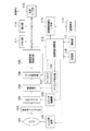
<デジタルスチルカメラのブロック図>
図1は、本発明の実施形態に係るデジタルスチルカメラの概略構成を示すブロック図である。このデジタルスチルカメラでは、レンズ101が被写体からの入射光を撮像素子106の撮像面に結像させ、その際に、レンズ駆動部102がレンズ101のズームやフォーカス、絞り等を駆動する。赤外カットフィルタ103は入射光の赤外領域の波長をカットする。
<Block diagram of digital still camera>
FIG. 1 is a block diagram showing a schematic configuration of a digital still camera according to an embodiment of the present invention. In this digital still camera, the
メカニカルシャッタ104は、撮像素子106に照射される光を遮断し、メカニカルシャッタ駆動部105は、被写体撮影時にメカニカルシャッタ104を駆動し、一定期間、被写体からの光を撮像素子106に露光させる。すなわち、メカニカルシャッタ104及びメカニカルシャッタ駆動部105は、レンズ101を通して撮像素子106に結像される光の透光/遮光を制御する遮光手段として機能する。
The
撮像素子106は、撮像素子106に結像した光学像を電気信号であるアナログ電圧に変換し、A/D変換器108へ出力する。なお、本実施形態では、撮像素子106はCCDであるものとする。サーミスタ107は、撮像素子106の周辺温度を検知し、A/D変換器108は、アナログ電圧を所定のビット数を持つデジタル信号に変換する。撮像信号処理回路109は、A/D変換器108で変換されたデジタル値に対して、ホワイトバランス制御等の補正や圧縮等の信号処理を行って、画像データを作成する。タイミング発生部110は、撮像素子106を駆動させるためのタイミング生成を行う。
The
メモリ部111は、画像データや撮影条件等を記憶し、全体制御演算部(CPU)112は、デジタルスチルカメラの全体的制御と各種演算を行う。記憶媒体制御インタフェース部113は、記憶媒体に対する画像データの書き込み/読み出しを行う。表示部114は、画像データの表示やユーザインタフェースの表示等を行う。
The
記憶媒体115は、例えば、デジタルスチルカメラの本体部に対して着脱自在な半導体メモリ等であり、画像データを最終フォーマットで記憶する。外部インタフェース部116は、外部装置であるPC等と通信を行うためのインタフェースである。測光部117は、被写体の明るさ情報を検出し、測距部118は、被写体までの距離情報を検出する。
The
図2は、メモリ部111の機能を模式的に示す図である。カメラ基本動作実行プログラム121は、デジタルスチルカメラの基本動作を行うプログラムであり、全体制御演算部112により実行される。輝度シェーディング補正プログラム122は、輝度シェーディング補正を実行するプログラムであり、全体制御演算部112により実行される。画像用一時記憶メモリ123は、撮像信号処理回路109での信号処理に際して一時的に使用されるメモリである。輝度シェーディング基本補正データ124は、輝度シェーディング補正プログラム122の実行時に必要となるデータである。撮影条件記憶メモリ125は、撮影条件を一時的に記憶するメモリである。
FIG. 2 is a diagram schematically illustrating the function of the
<輝度シェーディング補正の第1実施形態>
図3は、輝度シェーディング補正方法の第1実施形態に係るフローチャートであり、図4は、図3に示すステップS302(暗電流ムラの検出)の詳細な内容を示すフローチャートである。
<First Embodiment of Luminance Shading Correction>
FIG. 3 is a flowchart according to the first embodiment of the luminance shading correction method, and FIG. 4 is a flowchart showing detailed contents of step S302 (detection of dark current unevenness) shown in FIG.
撮影が開始されると、全体制御演算部112は、先ず、メカニカルシャッタ駆動部105を介してメカニカルシャッタ104を駆動して、一定期間、被写体の光を撮像素子106に露光して撮影を行う。そして、全体制御演算部112は、今回の被写体撮影時の撮影条件を撮影条件記憶メモリ125に記憶し(ステップS301)、続いて、撮像素子106の画面内の暗電流ムラの検出を行う(ステップS302)。
When shooting is started, the overall
ここで、ステップS302の処理の詳細について、図4のフローチャートを参照して説明する。全体制御演算部112は、撮影条件記憶メモリ125に記憶されている撮影条件と同じ撮影条件で、メカニカルシャッタ104で光を遮光した状態、すなわち撮像素子106の暗電流成分のみの遮光画像(以後「黒画像」という)を撮影する(ステップS401)。
Here, details of the processing in step S302 will be described with reference to the flowchart of FIG. The overall
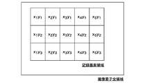
続いて、全体制御演算部112は、ステップS401で撮影した黒画像を複数の領域に分割する(ステップS402)。本実施形態では、升目状に、m×n(m,nは自然数)の領域に分割するものとし、CCD画面である撮像素子106の記録画素領域(有効画素部)を、X軸方向で5分割(m=5)し、Y軸方向で3分割(n=3)して、黒画像を15領域に分割する。図6は、撮像素子106の記録画素領域をX軸方向で5分割し、Y軸方向で3分割した状態を模式的示す図であり、xmyn(m=1〜5、n=1〜3)で示される15領域に分割されていることがわかる。
Subsequently, the overall
なお、m×nの領域分割数を多くすることによって、輝度シェーディング補正の精度を高めることができるが、演算速度は遅くなる(演算時間が長くなる)ため、精度と演算速度とのバランスを取った領域数を設定することが好ましい。また、領域分割に代えて、任意の領域を設定するようにしてもよい。 Increasing the number of m × n area divisions can improve the accuracy of luminance shading correction, but the calculation speed is slow (the calculation time is long), so the balance between accuracy and calculation speed is balanced. It is preferable to set the number of areas. Further, an arbitrary area may be set instead of the area division.
次に、全体制御演算部112は、黒画像に対して設定した15領域のそれぞれについて、暗電流ムラ量を示す演算値としての輝度値を算出する(ステップS403)。本実施形態では、暗電流ムラ量Yを“Y=Gr+Gb+R+B”で求めるものとする。但し、これに限定されず、暗電流量を表現できる演算値、演算式であれば他の演算値、演算式を用いても構わない。
Next, the overall
全体制御演算部112は、15領域のうち暗電流ムラ量Yの最も大きな値〔Ymax〕と、暗電流ムラ量〔Ymax〕が存在する領域である暗電流最大値領域〔xm(max)yn(max)〕とを輝度シェーディング基本補正データ124に記憶する(ステップS404)。
Total
ステップS404の処理の終了後、全体制御演算部112は、処理を図3のフローチャートのステップS303に進め、輝度シェーディング補正テーブルを参照する。そして、全体制御演算部112は、輝度シェーディング補正を実行するか否かを決定し、実行する場合には補正に用いる補正カーブを決定する(ステップS304)。
After completion of the process in step S404, the overall
輝度シェーディング補正テーブルは、暗電流ムラ量〔Ymax〕と暗電流最大値領域〔xm(max)yn(max)〕とによって輝度シェーディング補正カーブを決定するためのテーブルである。輝度シェーディング補正テーブル及び輝度シェーディング補正の実行/非実行についての詳細は後述する。 The luminance shading correction table is a table for determining a luminance shading correction curve based on the dark current unevenness amount [Y max ] and the dark current maximum value region [x m (max) y n (max) ]. Details of the luminance shading correction table and the execution / non-execution of the luminance shading correction will be described later.
輝度シェーディング補正を実行しない場合(S304でNO)、全体制御演算部112は、処理をステップS306に進めて画像作成を行う。一方、輝度シェーディング補正を実行する場合(S304でYES)、全体制御演算部112は、ステップS304で決定した条件で輝度シェーディング補正を行い(ステップS305)、その後、画像作成を行う(ステップS306)。
When the luminance shading correction is not executed (NO in S304), the overall
ステップS306の画像作成では、全体制御演算部112は、より具体的には、ステップS301で撮影した画像信号に対して信号処理を行い、記憶媒体に最終フォーマットで記憶する。ステップS306が終了すると、処理は終了となる。
More specifically, in the image creation in step S306, the overall
[ステップS303,304の詳細]
ステップS303で用いる輝度シェーディング補正テーブル及びステップS304での輝度シェーディング補正の実行/非実行の詳細について説明する。
[Details of Steps S303 and 304]
Details of the luminance shading correction table used in step S303 and the execution / non-execution of the luminance shading correction in step S304 will be described.
輝度シェーディング補正テーブルは、製品設計段階で暗電流ムラ量〔Ymax〕と輝度シェーディング補正量の検討を行うことにより作成される。輝度シェーディング補正テーブルは、以下に説明する(1)〜(4)の4点を考慮して作成される。
(1)暗電流ムラ量〔Ymax〕が大きいときに輝度シェーディング補正を行う場合には、暗電流ムラが画像品質を低下させる可能性が大きいため、画像品質を低下させないように輝度シェーディング補正量を小さく設定する。
(2)暗電流ムラ量〔Ymax〕が小さいときに輝度シェーディング補正を行う場合には、暗電流ムラが画像品質を低下させる可能性が小さいため、輝度シェーディング補正量を本来の希望の補正量に近づける。なお、「本来の希望の補正量」とは、輝度シェーディング補正時に、画面周辺部の画質低下に影響を与える暗電流ムラ等の画質低下要因が無い場合に設定可能な理想的な輝度シェーディング補正量である。
(3)暗電流ムラ量〔Ymax〕の存在する領域が撮像素子106の記録画素領域の周辺部に対応する場合、輝度シェーディング補正量を小さく設定する。
(4)暗電流ムラ量〔Ymax〕の存在する領域が撮像素子106の記録画素領域の中央部に対応する場合、輝度シェーディング補正量を本来希望の補正量に近づける。
The luminance shading correction table is created by examining the dark current unevenness amount [Y max ] and the luminance shading correction amount at the product design stage. The luminance shading correction table is created in consideration of the following four points (1) to (4) described below.
(1) When performing the luminance shading correction when the dark current unevenness amount [Y max ] is large, the dark current unevenness is likely to deteriorate the image quality. Therefore, the luminance shading correction amount is set so as not to deteriorate the image quality. Set to a smaller value.
(2) When performing the luminance shading correction when the dark current unevenness amount [Y max ] is small, the dark current unevenness is unlikely to deteriorate the image quality, so the luminance shading correction amount is set to the original desired correction amount. Move closer to. The “original desired correction amount” is an ideal luminance shading correction amount that can be set when there is no image quality degradation factor such as dark current unevenness that affects image quality degradation at the periphery of the screen during luminance shading correction. It is.
(3) When the region where the dark current unevenness amount [Y max ] exists corresponds to the peripheral portion of the recording pixel region of the
(4) When the region where the dark current unevenness amount [Y max ] is present corresponds to the central portion of the recording pixel region of the
図7は、撮像素子106の記録画素領域を上述の通りに15分割した場合における、輝度シェーディング補正量の領域分けの例を示す例である。図7では、上述の(3),(4)を考慮して、画面中心から対角までの像高に応じて領域A,領域B及び領域Cの3段階に領域設定を行っている。
FIG. 7 shows an example of luminance shading correction amount region division when the recording pixel region of the
図8及び図9を参照して後述する通り、本実施形態では、暗電流ムラ量〔Ymax〕の存在する領域に対応する撮像素子106の記録画素領域における位置に基づいて、輝度シェーディング補正量を決定する。例えば、撮像素子106の周辺部(像高が高い部分)である領域Cでは、輝度シェーディング補正量は小さく設定され、中央部(像高が低い部分)である領域Aでは、輝度シェーディング補正量は本来希望の補正量に設定される。
As will be described later with reference to FIGS. 8 and 9, in the present embodiment, the luminance shading correction amount is based on the position in the recording pixel region of the
図8は、製品設計段階で作成され、上述したステップS303で用いられる輝度シェーディング補正テーブルの一例を示す図である。輝度シェーディング補正テーブルを用いて、暗電流ムラ量〔Ymax〕及びその暗電流最大値領域〔xm(max)yn(max)〕が図7の領域A〜Cのどの領域に属しているかに基づいて、後述する図9に示すどの輝度シェーディング補正カーブを用いるかが決定される。 FIG. 8 is a diagram illustrating an example of the luminance shading correction table created in the product design stage and used in step S303 described above. Using the luminance shading correction table, which dark current unevenness amount [Y max ] and the dark current maximum value region [x m (max) y n (max) ] belong to the regions A to C in FIG. Based on the above, it is determined which luminance shading correction curve shown in FIG.
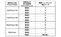
図9は、図8の輝度シェーディング補正テーブルに示される輝度シェーディング補正カーブを説明する図である。X軸は対角方向の像高であり、Y軸は輝度シェーディング補正量であり、撮像素子106の記録画素領域における周辺部の画素に対する増幅量を表している。本実施形態では、像高5割までは輝度シェーディング補正量を“1”としており、これは補正を行っていないことと等価である。像高5割から10割までは、補正無しから補正I〜Vまでの6種類の補正カーブが設けられており、補正Vが本来希望する輝度シェーディング補正量であり、補正Vから補正Iへ向かうにしたがって補正量は小さくなっている。
FIG. 9 is a diagram for explaining the luminance shading correction curve shown in the luminance shading correction table of FIG. The X-axis is the diagonal image height, the Y-axis is the luminance shading correction amount, and represents the amount of amplification with respect to the peripheral pixels in the recording pixel region of the
次に、図8の輝度シェーディング補正テーブルと暗電流ムラ量〔Ymax〕と暗電流最大値領域〔xm(max)yn(max)〕とにより、輝度シェーディング補正カーブが決定される過程を説明する。例えば、暗電流ムラ量〔Ymax〕が30LSB、暗電流最大値領域〔xm(max)yn(max)〕が領域Cであった場合、暗電流ムラ量〔Ymax〕が多く、領域も撮像素子106の記録画素領域の周辺部である。そのため、輝度シェーディング補正が画像品質を低下させる可能性が高いと判断し、輝度シェーディング補正を行わない補正無しのカーブとする。一方、暗電流ムラ量〔Ymax〕が5LSB、暗電流最大値領域〔xm(max)yn(max)〕が領域Aであった場合、暗電流ムラ量が小さく、領域も撮像素子106の記録画素領域の中央部付近である。そのため、輝度シェーディング補正が画像品質を低下させる可能性が低いと判断し、輝度シェーディング補正量を本来希望の補正カーブVとする。
Next, a process of determining a luminance shading correction curve based on the luminance shading correction table of FIG. 8, the dark current unevenness amount [Y max ], and the dark current maximum value region [x m (max) y n (max) ]. explain. For example, when the dark current unevenness amount [Y max ] is 30 LSB and the dark current maximum value region [x m (max) y n (max) ] is the region C, the dark current uneven amount [Y max ] is large and the region Is also the periphery of the recording pixel region of the
このように、図3のステップS304では輝度シェーディング補正の必要性が判断され、輝度シェーディング補正を行うと判断された場合には、補正に用いる補正カーブを決定し、ステップS305で輝度シェーディング補正が行われる。輝度シェーディング補正は、図8で決定した補正カーブで、図9に示した通りに像高に応じて撮像素子106の記録画素領域の画素毎に補正量を乗算することで補正を行う。
In this manner, the necessity of luminance shading correction is determined in step S304 in FIG. 3, and when it is determined that luminance shading correction is to be performed, a correction curve used for correction is determined, and luminance shading correction is performed in step S305. Is called. The luminance shading correction is performed by multiplying the correction amount for each pixel in the recording pixel area of the
<輝度シェーディング補正の第2実施形態>
図5は、輝度シェーディング補正方法の第2実施形態に係るフローチャートである。第1実施形態と同様に、全体制御演算部112は、メカニカルシャッタ104を駆動して、一定期間、被写体の光を撮像素子106に露光して撮影を行い、今回の被写体撮影時の撮影条件を撮影条件記憶メモリ125に記憶する(ステップS501)。そして、全体制御演算部112は、輝度シェーディング補正テーブルを参照する(ステップS502)。
<Second Embodiment of Luminance Shading Correction>
FIG. 5 is a flowchart according to the second embodiment of the luminance shading correction method. As in the first embodiment, the overall
第2実施形態で用いる輝度シェーディング補正テーブルは、被写体撮影時の撮影条件、特に暗電流ムラに影響を与える3つのパラメータ、すなわち、ISO感度、撮像素子106の周辺温度及びシャッタスピードにより算出される補正テーブルである。この輝度シェーディング補正テーブルは、製品設計段階でこれら3つのパラメータと暗電流ムラ量との関係について、以下の6点を考慮、検討して作成される。
(1)ISO感度設定が高い場合には、暗電流ムラが画像品質を低下させる可能性があるため、画像品質を低下させないように輝度シェーディング補正量を低く設定する。
(2)ISO感度設定が低い場合には、暗電流ムラが画像品質を低下させる可能性が小さいため、輝度シェーディング補正量を本来希望の補正量に近づける。
(3)被写体撮影時の撮像素子106の周辺温度が高い場合には、暗電流ムラが画像品質を低下させる可能性があるため、画像品質を低下させないように輝度シェーディング補正量を低く設定する。
(4)被写体撮影時の撮像素子106の周辺温度が低い場合には、暗電流ムラが画像品質を低下させる可能性が小さいため、輝度シェーディング補正量を本来希望の補正量に近づける。
(5)シャッタスピードが遅い場合には、暗電流ムラが画像品質を低下させる可能性があるため、画像品質を低下させないように輝度シェーディング補正量を低く設定する。
(6)シャッタスピードが速い場合には、暗電流ムラが画像品質を低下させる可能性が小さいため、輝度シェーディング補正量を本来希望の補正量に近づける。
The luminance shading correction table used in the second embodiment is a correction calculated based on three parameters that affect shooting conditions at the time of shooting a subject, particularly dark current unevenness, that is, ISO sensitivity, ambient temperature of the
(1) When the ISO sensitivity setting is high, dark current unevenness may reduce the image quality. Therefore, the luminance shading correction amount is set low so as not to reduce the image quality.
(2) When the ISO sensitivity setting is low, dark current unevenness is unlikely to deteriorate the image quality, so the luminance shading correction amount is brought close to the originally desired correction amount.
(3) When the ambient temperature of the
(4) When the ambient temperature of the
(5) When the shutter speed is slow, dark current unevenness may reduce the image quality, so the luminance shading correction amount is set low so as not to reduce the image quality.
(6) When the shutter speed is fast, dark current unevenness is unlikely to degrade the image quality, so the luminance shading correction amount is brought close to the originally desired correction amount.
図10は、ISO感度と被写体撮影時の撮像素子106の周辺温度Tとに基づいて輝度シェーディング補正量を決定する輝度シェーディング補正テーブルの例を示す図である。また、図11は、ISO感度とシャッタスピードTvとに基づいて輝度シェーディング補正量を決定する輝度シェーディング補正テーブルの例を示す図である。全体制御演算部112は、図10及び図11に示す輝度シェーディング補正テーブルを用いて、ISO感度、撮像素子106の周辺温度及びシャッタスピードにより、輝度シェーディング補正に用いる補正カーブを決定する(ステップS503)。
FIG. 10 is a diagram illustrating an example of a luminance shading correction table that determines the luminance shading correction amount based on the ISO sensitivity and the ambient temperature T of the
例えば、ISO感度設定が1600、撮像素子106の周辺温度が55℃であった場合、暗電流ムラ量が多いことが推定され、画像品質を低下させる可能性が高いと判断される。そのため、図10の輝度シェーディング補正テーブルから、補正を行わない補正無しの補正カーブが選択される。一方、ISO感度設定が200、撮像素子106の周辺温度が25℃であった場合、暗電流ムラ量が少ないことが推定され、画像品質を低下させる可能性が低いと判断される。そのため、図10の輝度シェーディング補正テーブルから、輝度シェーディング補正量を本来希望の補正量とする補正カーブVが選択される。
For example, when the ISO sensitivity setting is 1600 and the ambient temperature of the
同様に、ISO感度設定が1600、シャッタスピードが2sであった場合、暗電流ムラ量が多いことが推定され、画像品質を低下させる可能性が高いと判断される。そのため、図11の輝度シェーディング補正テーブルから、補正を行わない補正無しの補正カーブが選択される。一方、ISO感度設定が200、シャッタスピードが1/125sであった場合、暗電流ムラ量が少ないことが推定され、画像品質を低下させる可能性が低いと判断される。そのため、図11の輝度シェーディング補正テーブルから、輝度シェーディング補正量を本来希望の補正量とする補正カーブVが選択される。 Similarly, when the ISO sensitivity setting is 1600 and the shutter speed is 2 s, it is estimated that there is a large amount of dark current unevenness, and it is determined that there is a high possibility that the image quality will deteriorate. Therefore, a correction curve without correction without correction is selected from the luminance shading correction table of FIG. On the other hand, when the ISO sensitivity setting is 200 and the shutter speed is 1/125 s, it is estimated that the amount of dark current unevenness is small, and it is determined that there is a low possibility of reducing the image quality. Therefore, a correction curve V having the luminance shading correction amount as a desired correction amount is selected from the luminance shading correction table in FIG.
こうして、全体制御演算部112は、ステップS503において輝度シェーディング補正の必要性を判断し、輝度シェーディング補正を実行しない場合(S503でNO)、処理をステップS505に進めて画像作成を行う。一方、輝度シェーディング補正を実行する場合(S503でYES)、全体制御演算部112は、ステップS503で決定した条件で輝度シェーディング補正を行い(ステップS504)、その後、画像作成を行う(ステップS505)。ステップS505の処理は、第1実施形態で説明したステップS306の画像作成に準じて行われ、その後、処理は終了となる。
Thus, the overall
以上に説明した輝度シェーディング補正の第1及び第2の本実施形態によれば、撮像素子106で発生する画像周辺部の暗電流ムラの程度に応じて輝度シェーディング補正量を変化させる。そのため、画像周辺部の画像品質低下度合い、低下頻度を軽減することができ、高品質な画像を得ることが可能になる。
According to the first and second embodiments of the luminance shading correction described above, the luminance shading correction amount is changed according to the degree of dark current unevenness in the peripheral portion of the image generated by the
<他の実施形態>
以上、本発明をその好適な実施形態に基づいて詳述してきたが、本発明はこれら特定の実施形態に限られるものではなく、この発明の要旨を逸脱しない範囲の様々な形態も本発明に含まれる。さらに、上述した各実施形態は本発明の一実施形態を示すものにすぎず、各実施形態を適宜組み合わせることも可能である。
<Other embodiments>
Although the present invention has been described in detail based on preferred embodiments thereof, the present invention is not limited to these specific embodiments, and various forms within the scope of the present invention are also included in the present invention. included. Furthermore, each embodiment mentioned above shows only one embodiment of this invention, and it is also possible to combine each embodiment suitably.
例えば、輝度シェーディング補正の第1,第2実施形態のそれぞれにおいて、対角方向の像高に応じて輝度シェーディング補正を行うとしたが、水平方向と垂直方向のそれぞれの方向に応じて輝度シェーディング補正を行う構成としても構わない。また、輝度シェーディング補正の第2実施形態では、図10及び図11に示す2種類の輝度シェーディング補正テーブルを用いるとした。しかし、これに限定されず、ISO感度、撮像素子106の周辺温度及びシャッタスピードの組み合わせで1種類の輝度シェーディング補正テーブルを作成してもよいし、3種類以上の輝度シェーディング補正テーブルを作成しても構わない。
For example, in each of the first and second embodiments of the luminance shading correction, the luminance shading correction is performed according to the image height in the diagonal direction, but the luminance shading correction is performed according to the horizontal direction and the vertical direction. It does not matter even if it is the composition which performs. In the second embodiment of luminance shading correction, the two types of luminance shading correction tables shown in FIGS. 10 and 11 are used. However, the present invention is not limited to this, and one type of luminance shading correction table may be created by combining the ISO sensitivity, the ambient temperature of the
本発明は以下の処理を実行することによっても実現される。即ち、上述した実施形態の機能を実現するソフトウェア(プログラム)をネットワーク又は各種記憶媒体を介してシステム或いは装置に供給し、そのシステム或いは装置のコンピュータ(又はCPUやMPU等)がプログラムコードを読み出して実行する処理である。この場合、そのプログラム、及び該プログラムを記憶した記憶媒体は本発明を構成することになる。 The present invention can also be realized by executing the following processing. That is, software (program) that realizes the functions of the above-described embodiments is supplied to a system or apparatus via a network or various storage media, and a computer (or CPU, MPU, etc.) of the system or apparatus reads the program code. It is a process to be executed. In this case, the program and the storage medium storing the program constitute the present invention.
101 レンズ
104 メカニカルシャッタ
105 メカニカルシャッタ駆動部
106 撮像素子
109 撮像信号処理回路
111 メモリ部
112 全体制御演算部
DESCRIPTION OF
Claims (6)
前記レンズにより結像された光学像を電気信号に変換する撮像素子と、
前記撮像素子に結像される光の透光/遮光を制御する遮光手段と、
前記撮像素子から出力される電気信号を画像データに変換する信号処理手段と、
前記信号処理手段により変換された画像データに対して輝度シェーディング補正を行う補正手段と、
前記遮光手段により前記撮像素子が遮光された状態で遮光画像を撮影し、前記遮光画像に対応する画像データを複数の領域に分割し、各領域の画像データから暗電流量を求め、前記複数の領域のなかで前記暗電流量が相対的に大きい領域が前記撮像素子の記録画素領域の周辺部に位置する場合に、前記暗電流量が相対的に大きい領域が前記撮像素子の記録画素領域の中央部に位置する場合よりも前記補正手段が前記輝度シェーディング補正を行う際の補正量が小さくなるように制御する制御手段と、
を備えることを特徴とする撮像装置。 A lens for imaging light from the subject;
An image sensor that converts an optical image formed by the lens into an electrical signal;
A light shielding means for controlling light transmission / light shielding of light imaged on the image sensor;
Signal processing means for converting an electrical signal output from the image sensor into image data;
Correction means for performing luminance shading correction on the image data converted by the signal processing means;
Taking a light-shielded image in a state where the image sensor is shielded from light by the light-shielding means , dividing image data corresponding to the light-shielded image into a plurality of regions, obtaining a dark current amount from the image data of each region , When a region where the dark current amount is relatively large is located in a peripheral portion of the recording pixel region of the image sensor, the region where the dark current amount is relatively large is a region of the recording pixel region of the image sensor. Control means for controlling so that the correction amount when the correction means performs the luminance shading correction is smaller than the case where the correction means is located in a central portion ;
An imaging apparatus comprising:
前記撮像素子に結像する光の透光/遮光を制御する遮光手段により、前記撮像素子が遮光された状態で遮光画像を撮影する撮影ステップと、
前記撮影ステップで得られた遮光画像の画像データを複数の領域に分割し、各領域の画像データから暗電流量を求める演算ステップと、
前記複数の領域のなかで前記演算ステップで求めた前記暗電流量が相対的に大きい領域が前記撮像素子の記録画素領域の周辺部に位置する場合に、前記暗電流量が相対的に大きい領域が前記撮像素子の記録画素領域の中央部に位置する場合よりも輝度シェーディング補正を行う際の補正量が小さくなるように前記補正量を決定する決定ステップと、
前記決定ステップで決定された前記補正量に基づいて前記画像データに対して輝度シェーディング補正を行う補正ステップと、を有することを特徴とする撮像装置の制御方法。 An imaging device control method for converting an optical image into an electrical signal by an imaging device and converting an electrical signal output from the imaging device into image data,
A photographing step of photographing a light-shielded image in a state where the image sensor is shielded by a light shielding unit that controls transmission / shielding of light imaged on the image sensor ;
A calculation step of dividing the image data of the light-shielded image obtained in the photographing step into a plurality of regions and obtaining a dark current amount from the image data of each region ;
A region in which the dark current amount is relatively large when a region in which the dark current amount obtained in the calculation step is relatively large is located in a peripheral portion of the recording pixel region of the imaging element among the plurality of regions. Determining the correction amount so that the correction amount when performing the luminance shading correction is smaller than when located in the center of the recording pixel region of the image sensor ;
Control method for an imaging apparatus characterized by having a correction step of performing brightness shading correction on the image data based on the correction amount determined by the determining step.
Priority Applications (1)
| Application Number | Priority Date | Filing Date | Title |
|---|---|---|---|
| JP2011261751A JP5950552B2 (en) | 2011-11-30 | 2011-11-30 | IMAGING DEVICE AND IMAGING DEVICE CONTROL METHOD |
Applications Claiming Priority (1)
| Application Number | Priority Date | Filing Date | Title |
|---|---|---|---|
| JP2011261751A JP5950552B2 (en) | 2011-11-30 | 2011-11-30 | IMAGING DEVICE AND IMAGING DEVICE CONTROL METHOD |
Publications (3)
| Publication Number | Publication Date |
|---|---|
| JP2013115702A JP2013115702A (en) | 2013-06-10 |
| JP2013115702A5 JP2013115702A5 (en) | 2015-01-22 |
| JP5950552B2 true JP5950552B2 (en) | 2016-07-13 |
Family
ID=48710845
Family Applications (1)
| Application Number | Title | Priority Date | Filing Date |
|---|---|---|---|
| JP2011261751A Expired - Fee Related JP5950552B2 (en) | 2011-11-30 | 2011-11-30 | IMAGING DEVICE AND IMAGING DEVICE CONTROL METHOD |
Country Status (1)
| Country | Link |
|---|---|
| JP (1) | JP5950552B2 (en) |
Families Citing this family (2)
| Publication number | Priority date | Publication date | Assignee | Title |
|---|---|---|---|---|
| JP2015109582A (en) * | 2013-12-05 | 2015-06-11 | 三星電子株式会社Samsung Electronics Co.,Ltd. | Image processing device and image processing method |
| CN113709393B (en) * | 2021-08-20 | 2023-06-27 | 国光电器股份有限公司 | Calibration curve acquisition method and calibration method for optical dark area of image sensor |
Family Cites Families (4)
| Publication number | Priority date | Publication date | Assignee | Title |
|---|---|---|---|---|
| JP2006148791A (en) * | 2004-11-24 | 2006-06-08 | Canon Inc | Imaging device |
| JP2007027943A (en) * | 2005-07-13 | 2007-02-01 | Konica Minolta Photo Imaging Inc | Imaging apparatus, program and method for processing shading |
| JP2008124793A (en) * | 2006-11-13 | 2008-05-29 | Fujifilm Corp | Imaging apparatus and imaging method |
| JP5374217B2 (en) * | 2009-04-22 | 2013-12-25 | キヤノン株式会社 | Image processing apparatus and method |
-
2011
- 2011-11-30 JP JP2011261751A patent/JP5950552B2/en not_active Expired - Fee Related
Also Published As
| Publication number | Publication date |
|---|---|
| JP2013115702A (en) | 2013-06-10 |
Similar Documents
| Publication | Publication Date | Title |
|---|---|---|
| JP5616442B2 (en) | Imaging apparatus and image processing method | |
| JP5526014B2 (en) | Imaging device | |
| JP5162730B2 (en) | Imaging device and dark current correction method thereof | |
| CN102883108B (en) | Picture pick-up device and control method, image processing equipment and method | |
| JP6351271B2 (en) | Image composition apparatus, image composition method, and program | |
| US20190166320A1 (en) | Image processing apparatus, image processing method, and non-transitory computer readable recording medium | |
| JP5225137B2 (en) | Imaging apparatus, image processing method, and program | |
| JP5173664B2 (en) | Image processing apparatus and image processing method | |
| JP2011071709A (en) | Electronic camera | |
| US10630924B2 (en) | Image processing apparatus, image processing method, and non-transitory computer readable recording medium | |
| JP5950552B2 (en) | IMAGING DEVICE AND IMAGING DEVICE CONTROL METHOD | |
| JP4581633B2 (en) | Color signal correction method, apparatus and program | |
| JP5299159B2 (en) | Imaging apparatus and program | |
| JP2006180270A (en) | Image processing apparatus, imaging apparatus, image processing method, program, and recording medium | |
| JP6652666B2 (en) | Image sensor | |
| JP2012029194A (en) | Electronic camera and exposure control program | |
| JP2011135379A (en) | Imaging apparatus, imaging method and program | |
| JP2013115702A5 (en) | IMAGING DEVICE AND IMAGING DEVICE CONTROL METHOD | |
| JP5267290B2 (en) | Image processing apparatus, image processing method, and image processing program | |
| JP2012173943A (en) | Device and program for image processing | |
| JP6904560B2 (en) | Signal processing device | |
| JP2007295260A (en) | Image processing method and digital camera | |
| JP2024000839A (en) | Imaging device and image processing method | |
| JP2013115547A (en) | Imaging apparatus and control method of the same | |
| JP2009094675A (en) | Imaging apparatus, image signal processing circuit, image signal processing method, and computer program |
Legal Events
| Date | Code | Title | Description |
|---|---|---|---|
| A521 | Request for written amendment filed |
Free format text: JAPANESE INTERMEDIATE CODE: A523 Effective date: 20141128 |
|
| A621 | Written request for application examination |
Free format text: JAPANESE INTERMEDIATE CODE: A621 Effective date: 20141128 |
|
| A977 | Report on retrieval |
Free format text: JAPANESE INTERMEDIATE CODE: A971007 Effective date: 20151102 |
|
| A131 | Notification of reasons for refusal |
Free format text: JAPANESE INTERMEDIATE CODE: A131 Effective date: 20151110 |
|
| A521 | Request for written amendment filed |
Free format text: JAPANESE INTERMEDIATE CODE: A523 Effective date: 20160108 |
|
| TRDD | Decision of grant or rejection written | ||
| A01 | Written decision to grant a patent or to grant a registration (utility model) |
Free format text: JAPANESE INTERMEDIATE CODE: A01 Effective date: 20160510 |
|
| A61 | First payment of annual fees (during grant procedure) |
Free format text: JAPANESE INTERMEDIATE CODE: A61 Effective date: 20160607 |
|
| R151 | Written notification of patent or utility model registration |
Ref document number: 5950552 Country of ref document: JP Free format text: JAPANESE INTERMEDIATE CODE: R151 |
|
| LAPS | Cancellation because of no payment of annual fees |