JP5945269B2 - Pneumatic bearing with bonded polymer film wear surface and method of manufacturing the same - Google Patents
Pneumatic bearing with bonded polymer film wear surface and method of manufacturing the same Download PDFInfo
- Publication number
- JP5945269B2 JP5945269B2 JP2013515780A JP2013515780A JP5945269B2 JP 5945269 B2 JP5945269 B2 JP 5945269B2 JP 2013515780 A JP2013515780 A JP 2013515780A JP 2013515780 A JP2013515780 A JP 2013515780A JP 5945269 B2 JP5945269 B2 JP 5945269B2
- Authority
- JP
- Japan
- Prior art keywords
- substrate
- polymer film
- epoxy
- radiation
- bearing
- Prior art date
- Legal status (The legal status is an assumption and is not a legal conclusion. Google has not performed a legal analysis and makes no representation as to the accuracy of the status listed.)
- Active
Links
Images


Classifications
-
- B—PERFORMING OPERATIONS; TRANSPORTING
- B32—LAYERED PRODUCTS
- B32B—LAYERED PRODUCTS, i.e. PRODUCTS BUILT-UP OF STRATA OF FLAT OR NON-FLAT, e.g. CELLULAR OR HONEYCOMB, FORM
- B32B9/00—Layered products comprising a layer of a particular substance not covered by groups B32B11/00 - B32B29/00
- B32B9/005—Layered products comprising a layer of a particular substance not covered by groups B32B11/00 - B32B29/00 comprising one layer of ceramic material, e.g. porcelain, ceramic tile
-
- F—MECHANICAL ENGINEERING; LIGHTING; HEATING; WEAPONS; BLASTING
- F16—ENGINEERING ELEMENTS AND UNITS; GENERAL MEASURES FOR PRODUCING AND MAINTAINING EFFECTIVE FUNCTIONING OF MACHINES OR INSTALLATIONS; THERMAL INSULATION IN GENERAL
- F16C—SHAFTS; FLEXIBLE SHAFTS; ELEMENTS OR CRANKSHAFT MECHANISMS; ROTARY BODIES OTHER THAN GEARING ELEMENTS; BEARINGS
- F16C33/00—Parts of bearings; Special methods for making bearings or parts thereof
- F16C33/02—Parts of sliding-contact bearings
- F16C33/04—Brasses; Bushes; Linings
- F16C33/20—Sliding surface consisting mainly of plastics
-
- F—MECHANICAL ENGINEERING; LIGHTING; HEATING; WEAPONS; BLASTING
- F16—ENGINEERING ELEMENTS AND UNITS; GENERAL MEASURES FOR PRODUCING AND MAINTAINING EFFECTIVE FUNCTIONING OF MACHINES OR INSTALLATIONS; THERMAL INSULATION IN GENERAL
- F16C—SHAFTS; FLEXIBLE SHAFTS; ELEMENTS OR CRANKSHAFT MECHANISMS; ROTARY BODIES OTHER THAN GEARING ELEMENTS; BEARINGS
- F16C33/00—Parts of bearings; Special methods for making bearings or parts thereof
- F16C33/02—Parts of sliding-contact bearings
-
- B—PERFORMING OPERATIONS; TRANSPORTING
- B32—LAYERED PRODUCTS
- B32B—LAYERED PRODUCTS, i.e. PRODUCTS BUILT-UP OF STRATA OF FLAT OR NON-FLAT, e.g. CELLULAR OR HONEYCOMB, FORM
- B32B15/00—Layered products comprising a layer of metal
- B32B15/04—Layered products comprising a layer of metal comprising metal as the main or only constituent of a layer, which is next to another layer of the same or of a different material
- B32B15/08—Layered products comprising a layer of metal comprising metal as the main or only constituent of a layer, which is next to another layer of the same or of a different material of synthetic resin
-
- B—PERFORMING OPERATIONS; TRANSPORTING
- B32—LAYERED PRODUCTS
- B32B—LAYERED PRODUCTS, i.e. PRODUCTS BUILT-UP OF STRATA OF FLAT OR NON-FLAT, e.g. CELLULAR OR HONEYCOMB, FORM
- B32B15/00—Layered products comprising a layer of metal
- B32B15/18—Layered products comprising a layer of metal comprising iron or steel
-
- B—PERFORMING OPERATIONS; TRANSPORTING
- B32—LAYERED PRODUCTS
- B32B—LAYERED PRODUCTS, i.e. PRODUCTS BUILT-UP OF STRATA OF FLAT OR NON-FLAT, e.g. CELLULAR OR HONEYCOMB, FORM
- B32B27/00—Layered products comprising a layer of synthetic resin
- B32B27/06—Layered products comprising a layer of synthetic resin as the main or only constituent of a layer, which is next to another layer of the same or of a different material
- B32B27/08—Layered products comprising a layer of synthetic resin as the main or only constituent of a layer, which is next to another layer of the same or of a different material of synthetic resin
-
- B—PERFORMING OPERATIONS; TRANSPORTING
- B32—LAYERED PRODUCTS
- B32B—LAYERED PRODUCTS, i.e. PRODUCTS BUILT-UP OF STRATA OF FLAT OR NON-FLAT, e.g. CELLULAR OR HONEYCOMB, FORM
- B32B27/00—Layered products comprising a layer of synthetic resin
- B32B27/28—Layered products comprising a layer of synthetic resin comprising synthetic resins not wholly covered by any one of the sub-groups B32B27/30 - B32B27/42
- B32B27/281—Layered products comprising a layer of synthetic resin comprising synthetic resins not wholly covered by any one of the sub-groups B32B27/30 - B32B27/42 comprising polyimides
-
- B—PERFORMING OPERATIONS; TRANSPORTING
- B32—LAYERED PRODUCTS
- B32B—LAYERED PRODUCTS, i.e. PRODUCTS BUILT-UP OF STRATA OF FLAT OR NON-FLAT, e.g. CELLULAR OR HONEYCOMB, FORM
- B32B27/00—Layered products comprising a layer of synthetic resin
- B32B27/38—Layered products comprising a layer of synthetic resin comprising epoxy resins
-
- B—PERFORMING OPERATIONS; TRANSPORTING
- B32—LAYERED PRODUCTS
- B32B—LAYERED PRODUCTS, i.e. PRODUCTS BUILT-UP OF STRATA OF FLAT OR NON-FLAT, e.g. CELLULAR OR HONEYCOMB, FORM
- B32B9/00—Layered products comprising a layer of a particular substance not covered by groups B32B11/00 - B32B29/00
- B32B9/04—Layered products comprising a layer of a particular substance not covered by groups B32B11/00 - B32B29/00 comprising such particular substance as the main or only constituent of a layer, which is next to another layer of the same or of a different material
- B32B9/045—Layered products comprising a layer of a particular substance not covered by groups B32B11/00 - B32B29/00 comprising such particular substance as the main or only constituent of a layer, which is next to another layer of the same or of a different material of synthetic resin
-
- F—MECHANICAL ENGINEERING; LIGHTING; HEATING; WEAPONS; BLASTING
- F16—ENGINEERING ELEMENTS AND UNITS; GENERAL MEASURES FOR PRODUCING AND MAINTAINING EFFECTIVE FUNCTIONING OF MACHINES OR INSTALLATIONS; THERMAL INSULATION IN GENERAL
- F16C—SHAFTS; FLEXIBLE SHAFTS; ELEMENTS OR CRANKSHAFT MECHANISMS; ROTARY BODIES OTHER THAN GEARING ELEMENTS; BEARINGS
- F16C32/00—Bearings not otherwise provided for
- F16C32/06—Bearings not otherwise provided for with moving member supported by a fluid cushion formed, at least to a large extent, otherwise than by movement of the shaft, e.g. hydrostatic air-cushion bearings
-
- F—MECHANICAL ENGINEERING; LIGHTING; HEATING; WEAPONS; BLASTING
- F16—ENGINEERING ELEMENTS AND UNITS; GENERAL MEASURES FOR PRODUCING AND MAINTAINING EFFECTIVE FUNCTIONING OF MACHINES OR INSTALLATIONS; THERMAL INSULATION IN GENERAL
- F16C—SHAFTS; FLEXIBLE SHAFTS; ELEMENTS OR CRANKSHAFT MECHANISMS; ROTARY BODIES OTHER THAN GEARING ELEMENTS; BEARINGS
- F16C33/00—Parts of bearings; Special methods for making bearings or parts thereof
- F16C33/02—Parts of sliding-contact bearings
- F16C33/04—Brasses; Bushes; Linings
- F16C33/20—Sliding surface consisting mainly of plastics
- F16C33/201—Composition of the plastic
-
- F—MECHANICAL ENGINEERING; LIGHTING; HEATING; WEAPONS; BLASTING
- F16—ENGINEERING ELEMENTS AND UNITS; GENERAL MEASURES FOR PRODUCING AND MAINTAINING EFFECTIVE FUNCTIONING OF MACHINES OR INSTALLATIONS; THERMAL INSULATION IN GENERAL
- F16C—SHAFTS; FLEXIBLE SHAFTS; ELEMENTS OR CRANKSHAFT MECHANISMS; ROTARY BODIES OTHER THAN GEARING ELEMENTS; BEARINGS
- F16C43/00—Assembling bearings
- F16C43/02—Assembling sliding-contact bearings
-
- B—PERFORMING OPERATIONS; TRANSPORTING
- B32—LAYERED PRODUCTS
- B32B—LAYERED PRODUCTS, i.e. PRODUCTS BUILT-UP OF STRATA OF FLAT OR NON-FLAT, e.g. CELLULAR OR HONEYCOMB, FORM
- B32B2307/00—Properties of the layers or laminate
- B32B2307/50—Properties of the layers or laminate having particular mechanical properties
- B32B2307/536—Hardness
-
- B—PERFORMING OPERATIONS; TRANSPORTING
- B32—LAYERED PRODUCTS
- B32B—LAYERED PRODUCTS, i.e. PRODUCTS BUILT-UP OF STRATA OF FLAT OR NON-FLAT, e.g. CELLULAR OR HONEYCOMB, FORM
- B32B2307/00—Properties of the layers or laminate
- B32B2307/50—Properties of the layers or laminate having particular mechanical properties
- B32B2307/558—Impact strength, toughness
-
- B—PERFORMING OPERATIONS; TRANSPORTING
- B32—LAYERED PRODUCTS
- B32B—LAYERED PRODUCTS, i.e. PRODUCTS BUILT-UP OF STRATA OF FLAT OR NON-FLAT, e.g. CELLULAR OR HONEYCOMB, FORM
- B32B2307/00—Properties of the layers or laminate
- B32B2307/70—Other properties
- B32B2307/732—Dimensional properties
-
- B—PERFORMING OPERATIONS; TRANSPORTING
- B32—LAYERED PRODUCTS
- B32B—LAYERED PRODUCTS, i.e. PRODUCTS BUILT-UP OF STRATA OF FLAT OR NON-FLAT, e.g. CELLULAR OR HONEYCOMB, FORM
- B32B2457/00—Electrical equipment
- B32B2457/08—PCBs, i.e. printed circuit boards
-
- Y—GENERAL TAGGING OF NEW TECHNOLOGICAL DEVELOPMENTS; GENERAL TAGGING OF CROSS-SECTIONAL TECHNOLOGIES SPANNING OVER SEVERAL SECTIONS OF THE IPC; TECHNICAL SUBJECTS COVERED BY FORMER USPC CROSS-REFERENCE ART COLLECTIONS [XRACs] AND DIGESTS
- Y10—TECHNICAL SUBJECTS COVERED BY FORMER USPC
- Y10T—TECHNICAL SUBJECTS COVERED BY FORMER US CLASSIFICATION
- Y10T156/00—Adhesive bonding and miscellaneous chemical manufacture
- Y10T156/10—Methods of surface bonding and/or assembly therefor
- Y10T156/1052—Methods of surface bonding and/or assembly therefor with cutting, punching, tearing or severing
Description
関連出願への相互参照
[0001] 本願は、2010年6月23日に出願した米国仮出願第61/357,771号の優先権を主張し、その全体を本願に参考として組み込む。
Cross-reference to related applications
[0001] This application claims the priority of US Provisional Application No. 61 / 357,771 filed on June 23, 2010, the entirety of which is incorporated herein by reference.
[0002] 本発明は、一般に、リソグラフィに関し、より詳細には、空気軸受に関する。 [0002] The present invention relates generally to lithography, and more particularly to air bearings.
[0003] リソグラフィは、集積回路(IC)、ならびに他のデバイスおよび構造を製造するための重要なプロセスとして広く認識されている。リソグラフィ装置は、リソグラフィ中に使用される、パターンを基板上、例えば、基板のターゲット部分上に付与する機械である。リソグラフィ装置を用いたICの製造中、パターニングデバイス(マスクまたはレチクルとも呼ばれる)は、ICにおける個々の層上に形成される回路パターンを生成する。このパターンは、基板(例えば、シリコンウェーハ)上のターゲット部分(例えば、ダイの一部、または1つ以上のダイを含む)に転写することができる。通常、パターンの転写は、基板上に設けられた放射感応性材料(例えば、レジスト)層上への結像によって行われる。一般には、単一の基板が、連続的にパターニングされる隣接したターゲット部分のネットワークを含んでいる。ICの異なる層を製造することは、多くの場合、異なるレチクルを有する異なる層上に異なるパターンを結像することを要求する。したがって、レチクルおよび基板はリソグラフィプロセス中に変更される必要がある。レチクルハンドリングを容易にするために、レチクルを支持するステージには空気軸受が設けられる。 [0003] Lithography is widely recognized as an important process for fabricating integrated circuits (ICs) and other devices and structures. A lithographic apparatus is a machine used during lithography to apply a pattern onto a substrate, for example onto a target portion of the substrate. During the manufacture of an IC using a lithographic apparatus, a patterning device (also referred to as a mask or a reticle) generates a circuit pattern that is formed on an individual layer in the IC. This pattern can be transferred onto a target portion (eg including part of, one, or more dies) on a substrate (eg a silicon wafer). Usually, the pattern is transferred by imaging onto a radiation-sensitive material (eg, resist) layer provided on the substrate. In general, a single substrate will contain a network of adjacent target portions that are successively patterned. Manufacturing different layers of an IC often requires imaging different patterns on different layers with different reticles. Therefore, the reticle and substrate need to be changed during the lithography process. In order to facilitate reticle handling, an air bearing is provided on the stage that supports the reticle.
[0004] 軸受は、可動部分間の摩擦を減らし、および/または可動荷重を支持するデバイスである。軸受には主に2つの種類がある。減摩軸受は、ころ軸受または玉軸受などのデバイスを用いて摩擦を最小にする。摩擦軸受は、活性潤滑または可動部分間の動作を容易にするための他の手段を用いて摩擦を最小にする。摩擦軸受は滑り軸受としても知られている。多数の軸受アセンブリは、両方の原理、例えば、潤滑玉軸受アセンブリを利用する。 [0004] A bearing is a device that reduces friction between moving parts and / or supports moving loads. There are two main types of bearings. Antifriction bearings use devices such as roller bearings or ball bearings to minimize friction. Friction bearings minimize friction using active lubrication or other means to facilitate movement between moving parts. Friction bearings are also known as sliding bearings. Many bearing assemblies utilize both principles, such as a lubricated ball bearing assembly.
[0005] 空気軸受は摩擦または滑り軸受の一例である。これは、圧縮ガスを用いて軸受面が載せられて移動する均一なガスフィルムを生成する。ガスフィルムは、空気軸受の表面間で平滑な動作を容易にする事実上ほぼ摩擦のない潤滑剤として機能する。潤滑ガスフィルムが生成される軸受面を「活性表面」と呼ぶ。一般的に、空気軸受は、潤滑ガスフィルムを維持するために少なくとも安定した圧縮ガス源を必要とする。 [0005] An air bearing is an example of a friction or sliding bearing. This produces a uniform gas film on which the bearing surface is moved using compressed gas. The gas film functions as a virtually friction-free lubricant that facilitates smooth operation between the surfaces of the air bearing. The bearing surface on which the lubricating gas film is generated is called the “active surface”. In general, air bearings require at least a stable compressed gas source to maintain the lubricating gas film.
[0006] 上記したように、空気軸受のための例示的環境は、半導体のリソグラフィ分野にある。ここで、空気軸受には多数の利点が与えられる。空気軸受には事実上摩擦がなく、したがって、軸受が動作するときに微粒子の磨耗材料を生成しない。そのような微粒子物質は、超清浄半導体製造環境において面倒なことになり得る。さらに、玉またはころ軸受に存在する潤滑剤は、半導体製造環境に有害である汚染分子からガスを放出することができる。空気軸受は、さらに、比較的少ないメンテナンスまたは定期的な修理を必要とする。 [0006] As noted above, an exemplary environment for an air bearing is in the field of semiconductor lithography. Here, the air bearing has a number of advantages. Air bearings are virtually free of friction and, therefore, do not produce particulate wear material when the bearing operates. Such particulate matter can be troublesome in an ultra-clean semiconductor manufacturing environment. In addition, lubricants present in ball or roller bearings can release gases from contaminating molecules that are detrimental to the semiconductor manufacturing environment. Air bearings also require relatively little maintenance or regular repairs.
[0007] これら全ての利点にもかかわらず、空気軸受表面間の偶発的な「ドライ」接触が使用中に起きて従来の空気軸受表面を引っ掻きその性能に欠陥を生じさせる。この問題を解決するために、従来の軸受が研磨された花崗岩またはクロムめっき鋼の案内路に乗る一方、軸受自体は浸炭ステンレス鋼によって加工されている。浸炭プロセスは、鋼のスキン層を硬化させることによって耐摩耗性、耐腐食性および耐摩損性を提供する。鋼の大部分は硬化されないままであり、したがって、硬度は表面で最大であり、表面からの距離の直接関数としてスキン層の厚さを介して迅速かつ連続的に減る。あいにく、浸炭プロセスは、軸受が再粉砕されることを要求して軸受を僅かに変形させ、これは部分的かつ少し不均一に硬化された層を取り除く。最終製品は機能的かつ平坦な軸受であるが、硬化されたスキン層の厚さは軸受表面にわたって均一ではない。さらに、その厚さは、平坦性を回復させるために必要とされた粉砕の深さによって軸受ごとに異なる。実際には、軸受の硬度は浸炭プロセスによって厳密に制御することはできない。 [0007] Despite all these advantages, accidental “dry” contact between the air bearing surfaces occurs during use, scratching the conventional air bearing surface and causing a deficiency in its performance. To solve this problem, conventional bearings ride on polished granite or chrome-plated steel guideways, while the bearings themselves are machined from carburized stainless steel. The carburizing process provides wear resistance, corrosion resistance and abrasion resistance by hardening the steel skin layer. Most of the steel remains unhardened, so the hardness is greatest at the surface and decreases rapidly and continuously through the thickness of the skin layer as a direct function of the distance from the surface. Unfortunately, the carburizing process requires the bearing to be reground and slightly deforms the bearing, which removes a partially and slightly non-uniformly cured layer. The final product is a functional and flat bearing, but the thickness of the cured skin layer is not uniform across the bearing surface. Further, the thickness varies from bearing to bearing depending on the depth of grinding required to restore flatness. In practice, the bearing hardness cannot be strictly controlled by the carburizing process.
[0008] 硬化したスキン層の不均一性は、リソグラフィレチクルハンドラモジュールで使用される異なるシール軸受の場合に悪化する。このシール軸受はステージ軸受より一段階大きく、薄い鋼板から成る。薄い鋼板は、その部分の加熱を必要とする浸炭プロセスを含むあらゆる処理によって永久的に変形する傾向がある。真空環境においては、浸炭鋼は、良好な耐摩損性を提供し、過度の量の粒子を生成せず、比較的低価格である。したがって、これは従来最適な表面処理であった。 [0008] The non-uniformity of the cured skin layer is exacerbated for different sealed bearings used in lithographic reticle handler modules. This sealed bearing is one stage larger than the stage bearing and is made of a thin steel plate. Thin steel plates tend to be permanently deformed by any process, including carburizing processes that require heating of the part. In a vacuum environment, carburized steel provides good wear resistance, does not produce excessive amounts of particles, and is relatively inexpensive. Therefore, this has conventionally been the optimum surface treatment.
[0009] 空気軸受設計の改善は常に必要とされている。これは、製造ツールがより正確な許容差かつより早い速度へと常に押し進められる半導体リソグラフィツールの分野において特に当てはまる。 [0009] Improvements in air bearing design are always needed. This is especially true in the field of semiconductor lithography tools where manufacturing tools are constantly pushed to more precise tolerances and faster speeds.
[0010] 上記を踏まえると、真空対応であって軸受にガスが入力されないときに乾燥滑りを含むあらゆる潤滑なしで動作することができる空気軸受面を生成する方法が必要である。さらに、真空チャンバの汚染を防止するためにそのような状況下で非常に少ない粒子(ある場合)を生成する空気軸受面が必要である。改善される空気軸受は低価格であるべきである。これらの要求を満たすために、本発明の実施形態は、結合ポリマフィルム磨耗面を有する空気軸受およびその製造方法に関する。 In view of the above, there is a need for a method of generating an air bearing surface that is vacuum compatible and can operate without any lubrication including dry slip when no gas is input to the bearing. Furthermore, an air bearing surface is required that produces very few particles (if any) under such circumstances to prevent contamination of the vacuum chamber. Improved air bearings should be low cost. In order to meet these requirements, embodiments of the present invention relate to an air bearing having a bonded polymer film wear surface and a method of manufacturing the same.
[0011] 例えば、本発明の一実施形態は、基板と、基板上に配置された結合層と、結合層上に配置されたポリイミドフィルムとを含む軸受面を有する空気軸受を提供する。基板はセラミック材料であってよく、結合層は、ビスフェノールAのジグリシジルエーテル、1,4−ブタンジオールジグリシジルエーテルおよび2,2,4−トリメチルヘキサメチレン−1,6−ジアミンを含んでよい。ポリイミドフィルムは、ポリオキシジフェニレンピロメリットイミドを含み、約7〜100ミクロンの範囲にあってよく、少なくとも厚さ25ミクロンであることが好ましい。空気軸受はリソグラフィ装置で使用することができる。 [0011] For example, one embodiment of the present invention provides an air bearing having a bearing surface that includes a substrate, a bonding layer disposed on the substrate, and a polyimide film disposed on the bonding layer. The substrate may be a ceramic material and the tie layer may comprise diglycidyl ether of bisphenol A, 1,4-butanediol diglycidyl ether and 2,2,4-trimethylhexamethylene-1,6-diamine. The polyimide film comprises polyoxydiphenylene pyromellitic imide, may be in the range of about 7-100 microns, and is preferably at least 25 microns thick. Air bearings can be used in lithographic apparatus.
[0012] さらなる例では、本発明の一実施形態は、空気軸受の軸受面を製造する方法を提供する。方法は、真空チャックの平面上にポリイミドフィルムを配置することと、ポリイミドフィルムに真空を適用することと、ポリイミドフィルムの表面上に液状エポキシを配置することとを含んでよい。ポリイミドフィルムを基板と接触させずに基板を液状エポキシ上に配置することができる。基板は液状エポキシ上に解放され、重りは基板上に配置される。液状エポキシは硬化されて重りは除去される。ポリイミドフィルムは、真空チャックから剥離される。基板の外形と合うようにポリアミドフィルムをトリミングすることができる。 [0012] In a further example, an embodiment of the present invention provides a method of manufacturing a bearing surface of an air bearing. The method may include disposing a polyimide film on the plane of the vacuum chuck, applying a vacuum to the polyimide film, and disposing a liquid epoxy on the surface of the polyimide film. The substrate can be placed on the liquid epoxy without contacting the polyimide film with the substrate. The substrate is released on the liquid epoxy and the weight is placed on the substrate. The liquid epoxy is cured and the weight is removed. The polyimide film is peeled off from the vacuum chuck. The polyamide film can be trimmed to match the outer shape of the substrate.
[0013] 本発明のさらなる特徴および利点、ならびに本発明の様々な実施形態の構造および動作を、添付の図面を参照しながら以下に詳細に説明する。本発明は、本明細書で説明する特定の実施形態に限定されないことに留意されたい。このような実施形態は、本明細書では例示のためにのみ提示されている。本明細書に含まれる教示に基づき、当業者には追加の実施形態が明白になるであろう。 [0013] Further features and advantages of the present invention, as well as the structure and operation of various embodiments of the present invention, are described in detail below with reference to the accompanying drawings. It should be noted that the present invention is not limited to the specific embodiments described herein. Such embodiments are presented herein for illustrative purposes only. Based on the teachings contained herein, additional embodiments will become apparent to those skilled in the art.
[0014] 明細書に組み込まれ、本明細書の一部を形成する添付の図面は、本発明を図示し、さらに、記述とともに本発明の原理を説明し、当業者が本発明を作成して使用できるように役立つ。
[0021] 本発明における図は必ずしも縮尺通りに描かれていない。本発明の特徴および利点は、以下に述べる詳細な説明を図面と組み合わせて考慮することによりさらに明白になるであろう。ここで、同様の参照文字は全体を通して対応する要素を識別する。図面では、同様の参照番号は全体的に同一、機能的に類似する、および/または構造的に類似する要素を示す。要素が最初に現れた図面を、対応する参照番号の最も左側の(1つ以上の)桁で示す。 [0021] The drawings in the present invention are not necessarily drawn to scale. The features and advantages of the present invention will become more apparent from the detailed description set forth below when taken in conjunction with the drawings. Here, like reference characters identify corresponding elements throughout. In the drawings, like reference numbers generally indicate identical, functionally similar, and / or structurally similar elements. The drawing in which an element first appears is indicated by the leftmost digit (s) in the corresponding reference number.
1.概要
[0022] 本発明は、結合ポリマフィルム磨耗面およびその製造方法に関する。本明細書は、本発明の特徴を組み込んだ1つ以上の実施形態を開示する。開示される(1つ以上の)実施形態は、本発明を例示するに過ぎない。本発明の範囲は開示される(1つ以上の)実施形態に限定されない。本発明は添付の特許請求の範囲によって定義される。
1. Overview
[0022] The present invention relates to a bonded polymer film wear surface and a method of manufacturing the same. This specification discloses one or more embodiments that incorporate the features of this invention. The disclosed embodiment (s) are merely illustrative of the invention. The scope of the invention is not limited to the disclosed embodiment (s). The invention is defined by the appended claims.
[0023] 本説明は、半導体リソグラフィの分野の文脈において与えられる。この環境は、本発明の特定の特徴を上手く示すように選択される。しかしながら、環境は、添付の特許請求の範囲に記載された特徴を超えて本発明を限定するように解釈されるべきではない。当業者は、当然、半導体リソグラフィツールの文脈を超えて本明細書中に記載される特徴を有する空気軸受に対して多数の使用を想定する。 [0023] This description is given in the context of semiconductor lithography. This environment is selected to successfully demonstrate certain features of the invention. However, the environment should not be construed as limiting the invention beyond the features recited in the appended claims. Those skilled in the art will naturally envision numerous uses for air bearings having the features described herein beyond the context of semiconductor lithography tools.
[0024] 記載される実施形態、および「一実施形態」、「実施形態」、「例示的実施形態」などへの本明細書における言及は、記載される(1つ以上の)実施形態が特定の特徴、構造または特性を含むことができるが、それぞれの実施形態が必ずしも特定の特徴、構造または特性を含まないことを示す。さらに、そのようなフレーズは、必ずしも同じ実施形態に言及するものではない。さらに、一実施形態に関連して特定の特徴、構造または特性について記載している場合、明示的に記載されているか記載されていないかにかかわらず、そのような特徴、構造、または特性を他の実施形態との関連で実行することが当業者の知識にあることが理解される。 [0024] References herein to the described embodiment and "one embodiment", "embodiment", "exemplary embodiment" and the like are specific to the described (one or more) embodiments. Although each feature, structure or property may be included, each embodiment does not necessarily include a particular feature, structure or property. Moreover, such phrases are not necessarily referring to the same embodiment. Further, when a particular feature, structure, or characteristic is described in connection with one embodiment, such feature, structure, or characteristic may be expressed in a different manner, whether explicitly described or not. It is understood that it is within the knowledge of those skilled in the art to perform in the context of the embodiment.
[0025] 結合ポリマフィルム磨耗面を有する空気軸受およびその製造方法を開示する。例えば、ペイロード(payload)を支持するための空気軸受を開示する。空気軸受は、結合層によって基板に固定されたポリイミドフィルムを有する軸受面を有する。一実施形態では、ポリイミドフィルムは、ポリオキシジフェニレンピロメリットイミドを含み、結合層は、ビスフェノールAのジグリシジルエーテル、1,4−ブタンジオールジグリシジルエーテルおよび2,2,4−トリメチルヘキサメチレン−1,6−ジアミンを含む。軸受面は、真空対応であって軸受にガスが入力されないときに乾燥滑りを含むあらゆる潤滑なし動作をすることができる。さらに、チャンバの汚染を防止するために、軸受面は、乾燥滑り状況下で非常に少ない粒子を生成する。この解決策は、従来のエア軸受と比較したときに低価格でもある。 [0025] An air bearing having a bonded polymer film wear surface and a method of manufacturing the same are disclosed. For example, an air bearing for supporting a payload is disclosed. The air bearing has a bearing surface with a polyimide film fixed to the substrate by a bonding layer. In one embodiment, the polyimide film comprises polyoxydiphenylenepyromellitimide and the tie layer comprises diglycidyl ether of bisphenol A, 1,4-butanediol diglycidyl ether and 2,2,4-trimethylhexamethylene- Contains 1,6-diamine. The bearing surface is vacuum capable and can perform any lubrication-free operation including dry slip when no gas is input to the bearing. Furthermore, in order to prevent contamination of the chamber, the bearing surface produces very few particles under dry sliding conditions. This solution is also inexpensive when compared to conventional air bearings.
[0026] 本発明の実施形態は、低価格な材料および容易なプロセスを用いて有用かつ非常に平坦な工具面の複製を可能にする。費用のかかる精密な粉砕および熱処理ステップを回避する一方、高い性能、ロバスト性および耐久性が達成される。さらなる利点としては、真空環境における金属対金属の摩損が排除されることが挙げられる。 [0026] Embodiments of the present invention allow for the replication of useful and very flat tool surfaces using low cost materials and easy processes. High performance, robustness and durability are achieved while avoiding costly precision grinding and heat treatment steps. A further advantage is that metal-to-metal wear in a vacuum environment is eliminated.
[0027] これらおよび他の実施形態をより詳細に説明する前に、本発明の実施形態を実施することができる例示的環境を示すことが有益である。 [0027] Before describing these and other embodiments in more detail, it is useful to illustrate an exemplary environment in which embodiments of the present invention can be implemented.
II.例示的リソグラフィ環境
A.例示的反射型および透過型リソグラフィシステム
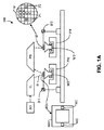
[0028] 図1Aおよび図1Bは、それぞれリソグラフィ装置100およびリソグラフィ装置100’を概略的に示す。リソグラフィ装置100およびリソグラフィ装置100’の各々は、放射ビームB(例えば、DUVまたはEUV放射)を調整するように構成された照明システム(イルミネータ)ILと、パターニングデバイス(例えば、マスク、レチクルまたは動的パターニングデバイス)MAを支持するように構成され、かつパターニングデバイスMAを正確に位置決めするように構成された第1ポジショナPMに連結されているサポート構造(例えば、マスクテーブル)MTと、基板(例えば、レジストコート基板)Wを保持するように構成され、かつ基板Wを正確に位置決めするように構成された第2ポジショナPWに連結されている基板テーブル(例えば、ウェーハテーブル)WTとを備える。リソグラフィ装置100および100’は、パターニングデバイスMAによって放射ビームBに付けられたパターンを基板Wのターゲット部分(例えば、1つ以上のダイを含む)C上に投影するように構成された投影システムPSも有する。リソグラフィ装置100では、パターニングデバイスMAおよび投影システムPSは反射型であり、リソグラフィ装置100’では、パターニングデバイスMAおよび投影システムPSは透過型である。
II. Exemplary Lithographic Environment A. Exemplary reflective and transmissive lithography systems
[0028] FIGS. 1A and 1B schematically depict a
[0029] 照明システムILとしては、放射Bを誘導し、整形し、または制御するために、屈折型、反射型、磁気型、電磁型、静電型、またはその他のタイプの光コンポーネント、あるいはそれらのあらゆる組合せなどのさまざまなタイプの光コンポーネントを含むことができる。 [0029] The illumination system IL may be a refractive, reflective, magnetic, electromagnetic, electrostatic, or other type of optical component, or the like, to induce, shape, or control the radiation B Various types of optical components, such as any combination of, can be included.
[0030] サポート構造MTは、パターニングデバイスMAの向き、リソグラフィ装置100および100’の設計、および、パターニングデバイスMAが真空環境内で保持されているか否かなどの他の条件に応じた態様で、パターニングデバイスMAを保持する。サポート構造MTは、機械式、真空式、静電式またはその他のクランプ技術を使って、パターニングデバイスMAを保持することができる。サポート構造MTは、例えば、必要に応じて固定または可動式にすることができるフレームまたはテーブルであってもよい。サポート構造MTは、パターニングデバイスを、例えば、投影システムPSに対して所望の位置に確実に置くことができる。
[0030] The support structure MT depends on the orientation of the patterning device MA, the design of the
[0031] 「パターニングデバイス」MAという用語は、基板Wのターゲット部分C内にパターンを作り出すように、放射ビームBの断面にパターンを与えるために使用できるあらゆるデバイスを指していると、広く解釈されるべきである。放射ビームBに付けたパターンは、集積回路などのターゲット部分C内に作り出されるデバイス内の特定の機能層に対応してもよい。 [0031] The term "patterning device" MA is broadly interpreted to refer to any device that can be used to pattern the cross section of the radiation beam B so as to create a pattern in the target portion C of the substrate W. Should be. The pattern applied to the radiation beam B may correspond to a particular functional layer in the device that is created in the target portion C, such as an integrated circuit.
[0032] パターニングデバイスMAは、透過型(図1Bのリソグラフィ装置100’のように)であっても、反射型(図1Aのリソグラフィ装置100のように)であってもよい。パターニングデバイスMAの例としては、レチクル、マスク、プログラマブルミラーアレイ、およびプログラマブルLCDパネルが含まれる。マスクは、リソグラフィでは公知であり、バイナリ、レベンソン型(alternating)位相シフト、およびハーフトーン型(attenuated)位相シフトなどのマスク型、ならびに種々のハイブリッドマスク型を含む。プログラマブルミラーアレイの一例では、小型ミラーのマトリックス配列が用いられており、各小型ミラーは、入射する放射ビームを様々な方向に反射させるように、個別に傾斜させることができる。傾斜されたミラーは、ミラーマトリックスによって反射される放射ビームBにパターンを付ける。
[0032] The patterning device MA may be transmissive (as in the lithographic apparatus 100 'of FIG. 1B) or reflective (as in the
[0033] 「投影システム」PSという用語は、使われている露光放射にとって、あるいは液浸液の使用または真空の使用といった他の要因にとって適切な、屈折型、反射型、反射屈折型、磁気型、電磁型、および静電型光学系、またはそれらのあらゆる組合せを含むあらゆる型の投影システムを包含し得る。EUVまたは電子ビーム放射に対しては真空環境が使用されてもよい。なぜなら、他のガスは放射または電子を吸収しすぎてしまう場合があるからである。したがって、真空環境は、真空壁および真空ポンプを用いてビームパス全体に提供されてよい。 [0033] The term "projection system" PS refers to refractive, reflective, catadioptric, magnetic types that are appropriate for the exposure radiation used or for other factors such as the use of immersion liquid or vacuum. Any type of projection system can be included, including electromagnetic, electrostatic and electrostatic optics, or any combination thereof. A vacuum environment may be used for EUV or electron beam radiation. This is because other gases may absorb too much radiation or electrons. Thus, a vacuum environment may be provided to the entire beam path using a vacuum wall and a vacuum pump.
[0034] リソグラフィ装置100および/またはリソグラフィ装置100’は、2つ(デュアルステージ)以上の基板テーブル(および/または2つ以上のマスクテーブル)WTを有する型のものであってもよい。そのような「マルチステージ」機械においては、追加の基板テーブルWTを並行して使うことができ、または予備工程を1つ以上のテーブル上で実行しつつ、別の1つ以上の基板テーブルWTを露光用に使うこともできる。リソグラフィ装置100では、装置の1つ以上の可動部分に空気(例えば、エア)軸受を設けることができる。例えば、基板テーブルWT、マスクテーブルMTおよびレチクルハンドリングデバイスなどのデバイスを空気軸受によって支持することができる。
[0034]
[0035] 図1Aおよび図1Bを参照すると、イルミネータILは、放射源SOから放射ビームを受ける。例えば、放射源SOがエキシマレーザである場合、放射源SOとリソグラフィ装置100および100’は、別個の構成要素であってもよい。そのような場合には、放射源SOは、リソグラフィ装置100または100’の一部を形成しているとはみなされず、また放射ビームBは、放射源SOからイルミネータILへ、例えば、適切な誘導ミラーおよび/またはビームエキスパンダを含むビームデリバリシステムBD(図1B)を使って送られる。その他の場合においては、例えば、放射源SOが水銀ランプである場合、放射源SOは、リソグラフィ装置100および100’の一体部分とすることもできる。放射源SOおよびイルミネータILは、必要ならばビームデリバリシステムBDとともに、放射システムと呼んでもよい。
[0035] Referring to FIGS. 1A and 1B, the illuminator IL receives a radiation beam from a radiation source SO. For example, if the source SO is an excimer laser, the source SO and the
[0036] イルミネータILは、放射ビームの角強度分布を調節するアジャスタAD(図1B)を含むことができる。一般に、イルミネータの瞳面内の強度分布の少なくとも外側および/または内側半径範囲(通常、それぞれσ-outerおよびσ-innerと呼ばれる)を調節することができる。さらに、イルミネータILは、インテグレータINおよびコンデンサCOといったさまざまな他のコンポーネント(図1B)を含むことができる。イルミネータILを使って放射ビームBを調整すれば、放射ビームの断面に所望の均一性および強度分布をもたせることができる。 [0036] The illuminator IL may include an adjuster AD (FIG. 1B) for adjusting the angular intensity distribution of the radiation beam. In general, at least the outer and / or inner radial extent (commonly referred to as σ-outer and σ-inner, respectively) of the intensity distribution in the illuminator pupil plane can be adjusted. Further, the illuminator IL may include various other components (FIG. 1B) such as an integrator IN and a capacitor CO. If the radiation beam B is adjusted using the illuminator IL, a desired uniformity and intensity distribution can be provided in the cross section of the radiation beam.
[0037] 図1Aを参照すると、放射ビームBは、サポート構造(例えば、マスクテーブル)MT上に保持されているパターニングデバイス(例えば、マスク)MA上に入射して、パターニングデバイスMAによってパターン形成される。リソグラフィ装置100では、パターニングデバイス(例えば、マスク)MAから放射ビームBが反射される。パターニングデバイス(例えば、マスク)MAから反射した後、放射ビームBは投影システムPSを通過し、投影システムPSは、基板Wのターゲット部分C上に放射ビームBの焦点をあわせる。第2ポジショナPWおよび位置センサIF2(例えば、干渉計デバイス、リニアエンコーダ、または静電容量センサ)を使って、例えば、さまざまなターゲット部分Cを放射ビームBのパス内に位置決めするように、基板テーブルWTを正確に動かすことができる。同様に、第1ポジショナPMおよび別の位置センサIF1を使い、パターニングデバイス(例えば、マスク)MAを放射ビームBのパスに対して正確に位置決めすることもできる。パターニングデバイス(例えば、マスク)MAおよび基板Wは、マスクアライメントマークM1およびM2と、基板アライメントマークP1およびP2とを使って、位置合わせされてもよい。
[0037] Referring to FIG. 1A, the radiation beam B is incident on the patterning device (eg, mask) MA, which is held on the support structure (eg, mask table) MT, and is patterned by the patterning device MA. The In the
[0038] 図1Bを参照すると、放射ビームBは、サポート構造(例えば、マスクテーブルMT)上に保持されているパターニングデバイス(例えば、マスクMA)上に入射して、パターニングデバイスによってパターン形成される。マスクMAを通り抜けた後、放射ビームBは投影システムPSを通過し、投影システムPSは、基板Wのターゲット部分C上にビームの焦点をあわせる。第2ポジショナPWおよび位置センサIF(例えば、干渉計デバイス、リニアエンコーダ、または静電容量センサ)を使って、例えば、さまざまなターゲット部分Cを放射ビームBの経路内に位置決めするように、基板テーブルWTを正確に動かすことができる。同様に、第1ポジショナPMおよび別の位置センサ(図1Bには明示的に示されていない)を使い、例えば、マスクライブラリからマスクを機械的に取り出した後またはスキャン中に、マスクMAを放射ビームBの経路に対して正確に位置決めすることもできる。 [0038] Referring to FIG. 1B, the radiation beam B is incident on the patterning device (eg, mask MA), which is held on the support structure (eg, mask table MT), and is patterned by the patterning device. . After passing through the mask MA, the radiation beam B passes through the projection system PS, which focuses the beam on the target portion C of the substrate W. The substrate table is used, for example, to position various target portions C in the path of the radiation beam B using a second positioner PW and a position sensor IF (eg, interferometer device, linear encoder, or capacitive sensor). The WT can be moved accurately. Similarly, the first positioner PM and another position sensor (not explicitly shown in FIG. 1B) are used to emit the mask MA after, for example, mechanical removal of the mask from the mask library or during a scan. It can also be accurately positioned with respect to the path of the beam B.
[0039] 通常、マスクテーブルMTの移動は、第1ポジショナPMの一部を形成するロングストロークモジュール(粗動位置決め)およびショートストロークモジュール(微動位置決め)を使って達成することができる。同様に、基板テーブルWTの移動も、第2ポジショナPWの一部を形成するロングストロークモジュールおよびショートストロークモジュールを使って達成することができる。ステッパの場合は(スキャナとは対照的に)、マスクテーブルMTは、ショートストロークアクチュエータのみに連結されてもよく、または固定されてもよい。マスクMAおよび基板Wは、マスクアライメントマークM1およびM2と、基板アライメントマークP1およびP2とを使って、位置合わせされてもよい。例示では基板アライメントマークが専用ターゲット部分を占めているが、基板アライメントマークをターゲット部分とターゲット部分との間の空間内に置くこともできる(これらは、スクライブラインアライメントマークとして公知である)。同様に、複数のダイがマスクMA上に設けられている場合、マスクアライメントマークは、ダイとダイの間に置かれてもよい。 Normally, the movement of the mask table MT can be achieved by using a long stroke module (coarse positioning) and a short stroke module (fine movement positioning) that form a part of the first positioner PM. Similarly, movement of the substrate table WT can also be achieved using a long stroke module and a short stroke module that form part of the second positioner PW. In the case of a stepper (as opposed to a scanner) the mask table MT may be connected to a short stroke actuator only, or may be fixed. Mask MA and substrate W may be aligned using mask alignment marks M1 and M2 and substrate alignment marks P1 and P2. In the example, the substrate alignment mark occupies the dedicated target portion, but the substrate alignment mark can also be placed in the space between the target portion (these are known as scribe line alignment marks). Similarly, if a plurality of dies are provided on the mask MA, the mask alignment mark may be placed between the dies.
[0040] リソグラフィ装置100および100’は、以下のモードのうち少なくとも1つのモードで使用できる。
[0040]
[0041] 1.ステップモードにおいては、サポート構造(例えば、マスクテーブル)MTおよび基板テーブルWTを基本的に静止状態に保ちつつ、放射ビームBに付けられたパターン全体を一度にターゲット部分C上に投影する(すなわち、単一静的露光)。その後、基板テーブルWTは、Xおよび/またはY方向に移動され、それによって別のターゲット部分Cを露光することができる。 [0041] In step mode, the entire pattern applied to the radiation beam B is projected onto the target portion C at once (ie, while the support structure (eg, mask table) MT and substrate table WT are essentially stationary) (ie, Single static exposure). Thereafter, the substrate table WT is moved in the X and / or Y direction so that another target portion C can be exposed.
[0042] 2.スキャンモードにおいては、サポート構造(例えば、マスクテーブル)MTおよび基板テーブルWTを同期的にスキャンする一方で、放射ビームBに付けられたパターンをターゲット部分C上に投影する(すなわち、単一動的露光)。サポート構造(例えば、マスクテーブル)MTに対する基板テーブルWTの速度および方向は、投影システムPSの(縮小)拡大率および像反転特性によって決めることができる。 [0042] 2. In scan mode, the support structure (eg, mask table) MT and substrate table WT are scanned synchronously while a pattern imparted to the radiation beam B is projected onto a target portion C (ie, a single dynamic exposure). ). The speed and direction of the substrate table WT relative to the support structure (eg mask table) MT can be determined by the (reduction) magnification factor and image reversal characteristics of the projection system PS.
[0043] 3.別のモードにおいては、プログラマブルパターニングデバイスを保持した状態で、サポート構造(例えば、マスクテーブル)MTを基本的に静止状態に保ち、また基板テーブルWTを動かす、またはスキャンする一方で、放射ビームBに付けられたパターンをターゲット部分C上に投影する。パルス放射源SOが採用されており、さらにプログラマブルパターニングデバイスは、基板テーブルWTの移動後ごとに、またはスキャン中の連続する放射パルスと放射パルスとの間に、必要に応じて更新される。この動作モードは、前述の型のプログラマブルミラーアレイといったプログラマブルパターニングデバイスを利用するマスクレスリソグラフィに容易に適用することができる。 [0043] 3. In another mode, with the programmable patterning device held, the support structure (eg mask table) MT is kept essentially stationary and the substrate table WT is moved or scanned while the radiation beam B is The attached pattern is projected onto the target portion C. A pulsed radiation source SO is employed and the programmable patterning device is updated as necessary after each movement of the substrate table WT or between successive radiation pulses during the scan. This mode of operation can be readily applied to maskless lithography that utilizes programmable patterning device, such as a programmable mirror array of a type as described above.
[0044] 上述の使用モードの組合せおよび/またはバリエーション、あるいは完全に異なる使用モードもまた採用可能である。 [0044] Combinations and / or variations on the above described modes of use or entirely different modes of use may also be employed.
[0045] 本明細書において、IC製造におけるリソグラフィ装置の使用について具体的な言及がなされているが、本明細書記載のリソグラフィ装置が、集積光学システム、磁気ドメインメモリ用のガイダンスパターンおよび検出パターン、フラットパネルディスプレイ、液晶ディスプレイ(LCD)、薄膜磁気ヘッド等の製造といった他の用途を有し得ることが理解されるべきである。当業者にとっては当然のことであるが、そのような別の用途においては、本明細書で使用される「基板」または「ダイ」という用語はすべて、それぞれより一般的な「基板」または「ターゲット部分」という用語と同義であるとみなしてよい。本明細書に記載した基板は、露光の前後を問わず、例えば、トラック(通常、基板にレジスト層を塗布し、かつ露光されたレジストを現像するツール)、メトロロジーツール、および/またはインスペクションツールで処理されてもよい。適用可能な場合には、本明細書中の開示内容を上記のような基板プロセシングツールおよびその他の基板プロセシングツールに適用してもよい。さらに基板は、例えば、多層ICを作るために複数回処理されてもよいので、本明細書で使用される基板という用語は、すでに多重処理層を包含している基板を表すものとしてもよい。 [0045] Although specific reference is made herein to the use of a lithographic apparatus in IC manufacturing, the lithographic apparatus described herein is an integrated optical system, a guidance pattern and a detection pattern for a magnetic domain memory, It should be understood that other applications such as the manufacture of flat panel displays, liquid crystal displays (LCDs), thin film magnetic heads and the like may be had. As will be appreciated by those skilled in the art, in such other applications, the terms “substrate” or “die” as used herein are all more general “substrate” or “target” respectively. It may be considered synonymous with the term “part”. The substrate described herein can be used, for example, before or after exposure, such as a track (usually a tool for applying a resist layer to the substrate and developing the exposed resist), a metrology tool, and / or an inspection tool. May be processed. Where applicable, the disclosure herein may be applied to substrate processing tools such as those described above and other substrate processing tools. Further, since the substrate may be processed multiple times, for example, to make a multi-layer IC, the term substrate as used herein may refer to a substrate that already contains multiple processing layers.
[0046] さらなる実施形態においては、リソグラフィ装置100は、EUVリソグラフィのためのEUV放射ビームを生成するように構成された極端紫外線(EUV)源を含む。一般には、EUV源は放射システム内に構成されており(下記参照)、対応する照明システムはEUV源のEUV放射ビームを調整するように構成されている。
[0046] In a further embodiment, the
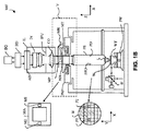
B.例示的EUVリソグラフィ装置
[0047] 図2は、本発明の一実施形態による例示的EUVリソグラフィ装置200を概略的に示す。図2では、EUVリソグラフィ装置200は、放射システム42、照明光学ユニット44および投影システムPSを含む。放射システム42は、放射ビームが放電プラズマによって形成され得る放射源SOを含む。一実施形態では、EUV放射は、電磁スペクトルのEUV範囲内の放射を放出するために非常に高温のプラズマが生成される、例えば、Xeガス、Li蒸気あるいはSn蒸気などのガスまたは蒸気によって生成され得る。非常に高温のプラズマは、少なくとも部分的にイオン化されたプラズマを、例えば、放電によって生成することによって作り出すことができる。例えば、10PaのXe、Li、Sn蒸気、あるいは任意の他の適したガスまたは蒸気の分圧が、放射の効率的な生成のために必要とされることがある。放射源SOによって放出される放射は、放射源チャンバ47から、放射源チャンバ47における開口部内またはその後方に位置決めされたガスバリアまたは汚染物質トラップ49を介してコレクタチャンバ48へと進む。一実施形態では、ガスバリア49はチャネル構造を含んでもよい。
B. Exemplary EUV lithography apparatus
[0047] Figure 2 schematically depicts an exemplary EUV
[0048] コレクタチャンバ48は、かすめ入射コレクタによって形成され得る放射コレクタ50(集光ミラーまたはコレクタとも呼ぶ)を含む。放射コレクタ50は、上流放射コレクタ側50aおよび下流放射コレクタ側50bを有する。コレクタ50を通った放射は、格子スペクトルフィルタ51から反射してコレクタチャンバ48内のアパーチャにおける仮想光源点52に合焦することができる。放射コレクタ50は、当業者には周知である。
[0048] The
[0049] 放射ビーム56は、集光チャンバ48から、法線入射リフレクタ53および54を介してレチクルまたはマスクテーブルMT上に位置決めされたレチクルまたはマスク(図示せず)上へと照明光学ユニット44内で反射する。パターン付きビーム57が形成され、これは、投影システムPSにおいて反射要素58および59を介してウェーハステージまたは基板テーブルWT上で支持された基板(図示せず)上に結像される。様々な実施形態では、照明光学ユニット44および投影システムPSは、図2に示されたものよりも多くの(または少ない)要素を含んでもよい。例えば、格子スペクトルフィルタ51は、リソグラフィ装置のタイプによって任意的に存在してもよい。さらに、一実施形態では、照明光学ユニット44および投影システムPSは、図2に示されたものよりも多くのミラーを含んでもよい。例えば、投影システムPSは、反射要素58および59に加えて1〜4個の反射要素を組み入れてもよい。図2では、参照番号180は2つのリフレクタ間の空間、例えば、リフレクタ142とリフレクタ143との間の空間を示す。
[0049] The radiation beam 56 enters the illumination
[0050] 一実施形態では、集光ミラー50は、かすめ入射ミラーの代わりにまたはそれに加えて法線入射コレクタを含んでもよい。さらに、集光ミラー50は、リフレクタ142、143および146を有する入れ子化されたコレクタについて記述されているが、本明細書中、コレクタの一例としてさらに使用されている。
[0050] In one embodiment, the
[0051] さらに、図2に概略的に示すような格子51の代わりに、透過型光フィルタが適用されてもよい。EUVが透過する光フィルタ、ならびにUV放射があまり透過せず、またはUV放射を実質的に吸収までもする光フィルタは、当業者には周知である。したがって、「格子スペクトル純度フィルタ」は、本明細書中、格子または透過型フィルタを含む「スペクトル純度フィルタ」としてほぼ同じ意味でさらに示される。図2には示されていないが、EUV透過型光フィルタは、例えば集光ミラー50の上流に構成された追加の光学要素、あるいは照明ユニット44および/または投影システムPSにおける光EUV透過型フィルタとして含まれてもよい。
Furthermore, a transmission type optical filter may be applied instead of the grating 51 as schematically shown in FIG. Optical filters that transmit EUV, as well as optical filters that transmit less UV radiation or even substantially absorb UV radiation, are well known to those skilled in the art. Accordingly, “grating spectral purity filter” is further referred to herein in substantially the same sense as a “spectral purity filter” including a grating or transmission filter. Although not shown in FIG. 2, the EUV transmissive optical filter is, for example, as an additional optical element configured upstream of the
[0052] 光学要素に対する「上流」および「下流」という用語は、それぞれ、1つ以上の追加の光学要素の「光学的上流」および「光学的下流」である1つ以上の光学要素の位置を示す。放射ビームがリソグラフィ装置200を通り抜ける光路に従って、第2光学要素より放射源SOに近い第1光学要素は第2光学要素の上流に構成され、第2光学要素は第1光学要素の下流に構成される。例えば、集光ミラー50がスペクトルフィルタ51の上流に構成されるのに対して、光学要素53はスペクトルフィルタ51の下流に構成される。
[0052] The terms "upstream" and "downstream" relative to an optical element refer to the position of one or more optical elements that are "optically upstream" and "optically downstream", respectively, of one or more additional optical elements. Show. According to the optical path through which the radiation beam passes through the
[0053] 図2に示される全ての光学要素(および本実施形態の概略図に示されていない追加の光学要素)には、例えばSnなどの放射源SOによって生成される汚染物質が堆積しやすいことがある。これは放射コレクタ50にも当てはまり、スペクトル純度フィルタ51が存在した場合にも当てはまる。したがって、洗浄デバイスがこれらの光学要素のうちの1つ以上を洗浄するために採用されるとともに洗浄方法がそれらの光学要素に適用されてもよいが、法線入射リフレクタ53および54、ならびに反射要素58および59、または追加のミラー、格子等の他の光学要素に適用されてもよい。
[0053] All optical elements shown in FIG. 2 (and additional optical elements not shown in the schematic diagram of the present embodiment) are likely to deposit contaminants generated by a radiation source SO such as Sn. Sometimes. This is also true for the
[0054] 放射コレクタ50はかすめ入射コレクタであってもよく、そのような実施形態では、コレクタ50は光軸Oに沿って位置合わせされる。放射源SOまたはその像は、光軸Oに沿って配置されてもよい。放射コレクタ50は、リフレクタ142、143および146(「シェル)」またはいくつかのWolter型リフレクタを含むWolter型リフレクタとしても公知である)を含んでもよい。リフレクタ142、143および146は、入れ子化され、光軸Oの周りで回転対称であってもよい。図2では、内側リフレクタは参照番号142で示され、中間リフレクタは参照番号143で示され、かつ外側リフレクタは参照番号146で示される。放射コレクタ50は、ある体積(すなわち(1つ以上の)外側リフレクタ146内の体積)を包囲する。通常、(1つ以上の)外側リフレクタ146内の体積は、小さな開口部が存在してもよいが、円周方向で閉じられている。
[0054] The
[0055] リフレクタ142、143および146のそれぞれは、その少なくとも一部が1層の反射層または多数の反射層を表す表面を含んでよい。したがって、リフレクタ142、143および146(あるいは3つより多いリフレクタまたはシェルを有する放射コレクタの実施形態における追加のリフレクタ)は、放射源SOからEUV放射を反射および集光するように少なくとも部分的に設計され、かつリフレクタ142、143および146の少なくとも一部は、EUV放射を反射および集光するように設計されないことがある。例えば、リフレクタの裏面の少なくとも一部は、EUV放射を反射および集光するように設計されない。これらの反射層の表面上には、反射層の表面の少なくとも一部の上に設けられる保護のためまたは光フィルタとしてのキャップ層があってもよい。
[0055] Each of the
[0056] 放射コレクタ50は、放射源SOまたは放射源SOの像の付近に配置されてよい。リフレクタ142、143および146の各々は、少なくとも2つの隣接する反射面を含んでよく、放射源SOから離れたほうに位置する反射面は、放射源SOに近いほうに位置する反射面よりも、光軸Oに対して小さな角度で配置される。このようにして、かすめ入射コレクタ50は、光軸Oに沿って伝搬するEUV放射ビームを生成するように構成される。少なくとも2つのリフレクタは、実質的に同軸に配置され、光軸Oの周りで実質的に回転対称に延在してもよい。放射コレクタ50が、外側リフレクタ146の外面上にさらなるフィーチャ、または外側リフレクタ146の周りにさらなるフィーチャ、例えば保護ホルダやヒータなどを有してもよいことが理解されたい。
[0056] The
[0057] 本明細書中に記載する実施形態において、「レンズ」および「レンズ要素」という用語は、文脈によっては、屈折、反射、磁気、電磁気、および静電型光コンポーネントを含む様々な種類の光コンポーネントのいずれか1つまたはこれらの組合せを指すことができる。 [0057] In the embodiments described herein, the terms "lens" and "lens element" are used in various types, including refractive, reflective, magnetic, electromagnetic, and electrostatic optical components, depending on the context. It can refer to any one or a combination of optical components.
[0058] 本明細書で使用する「放射」および「ビーム」という用語は、紫外線(UV)(例えば、365、248、193、157、または126nmの波長λを有する)、極端紫外線(EUVまたは軟X線)(例えば、5〜20nmの範囲の波長、例えば13.5nmの波長を有する)または5nm未満で働く硬X線、ならびにイオンビームや電子ビームなどの粒子ビームを含めた全てのタイプの電磁放射を包含している。一般に、約780〜3000nm(以上)の間の波長を有する放射がIR放射とみなされる。UVとは、約100〜400nmの波長を有する放射のことを指す。リソグラフィにおいて、UVは、水銀放電ランプによって生成することができる波長、すなわちG線436nm、H線405nmおよび/またはI線365nmにも当てはまる。真空UVまたはVUV(すなわち、空気によって吸収されるUV)とは、約100〜200nmの波長を有する放射のことを指す。深UV(DUV)とは、通常、126nm〜428nmの範囲の波長を有する放射のことを指し、一実施形態では、エキシマレーザがリソグラフィ装置内で使用されるDUV放射を生成することができる。当然のことながら、例えば5〜20nmの範囲内の波長を有する放射は、少なくともその一部が5〜20nmの範囲内にある特定の波長帯域を有する放射に関する。 [0058] As used herein, the terms "radiation" and "beam" refer to ultraviolet (UV) (eg, having a wavelength λ of 365, 248, 193, 157, or 126 nm), extreme ultraviolet (EUV or soft). X-rays) (for example, having a wavelength in the range of 5-20 nm, for example having a wavelength of 13.5 nm) or hard X-rays working below 5 nm, and all types of electromagnetics including particle beams such as ion beams and electron beams Includes radiation. In general, radiation having a wavelength between about 780 and 3000 nm (and above) is considered IR radiation. UV refers to radiation having a wavelength of about 100-400 nm. In lithography, UV also applies to wavelengths that can be generated by mercury discharge lamps, namely G-line 436 nm, H-line 405 nm and / or I-line 365 nm. Vacuum UV or VUV (ie UV absorbed by air) refers to radiation having a wavelength of about 100-200 nm. Deep UV (DUV) generally refers to radiation having a wavelength in the range of 126 nm to 428 nm, and in one embodiment, an excimer laser can generate DUV radiation for use in a lithographic apparatus. Of course, radiation having a wavelength in the range of, for example, 5-20 nm relates to radiation having a specific wavelength band, at least part of which is in the range of 5-20 nm.
III.改良空気軸受
A.結合ポリマフィルム磨耗面を有する平坦な空気軸受
[0059] 図3は、本発明による、結合ポリマフィルム磨耗面を有する例示的空気軸受300を示す。空気軸受300の一部として、ポリイミドフィルム302が結合剤306によって基板304に永久的に結合される。空気エア軸受300は、上記のリソグラフィ装置100および100’などのリソグラフィツールで使用することができる。例えば、基板304は、上記のリソグラフィ装置100および100’の一部であるレチクルハンドリングデバイスの一部としてペイロードを支持することができる。
III. Improved air bearing Flat air bearing with bonded polymer film wear surface
[0059] FIG. 3 illustrates an
[0060] ポリイミドフィルム302は丈夫で耐久性のあるポリマフィルムである。好ましいポリイミドフィルム302は、DuPont社によってフィルム形態で製造されKapton(登録商標)という商号の下で販売されているポリオキシジフェニレンピロメリットイミドである。例えば、ポリイミドフィルム302の厚さは、7〜100ミクロンの範囲であり、好ましくは、少なくとも25ミクロンである。
[0060] The
[0061] 好ましい結合剤306は、Epo−tek(登録商標)301−2エポキシという商号の下で販売されている、ビスフェノールAのジグリシジルエーテル、1,4−ブタンジオールジグリシジルエーテルおよび2,2,4−トリメチルヘキサメチレン−1,6−ジアミンなどの低い粘着性を有する、二部の室温硬化エポキシである。
[0061]
[0062] 基板304は非硬化面を有するため、軸受面を生成するためには丈夫で耐久性のあるポリマフィルムが非硬化基板に結合される。したがって、対向する軸受面はその自然で低歪みの非硬化状態のまま残すことができる。基板304は、例えばステンレス鋼などの金属であってよく、対向面は、例えばステンレス鋼などの同様なまたは異なる材料であってもよい。当業者には明らかであるが、基板304の材料の選択としては、例えば、ガラスおよびセラミックなどの高度の平坦性を達成するのに好ましい他の材料も挙げられる。非限定例では、基板304の厚さは約10ミリメートルおよび直径は約300ミリメートルであり、基板304の有用面にわたる表面の平坦性は山対谷約3〜約6ミクロンである。
[0062] Since
B.結合ポリマフィルム磨耗面を有する平坦な空気軸受を製造する方法
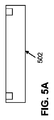
[0063] 図4は、空気軸受300などの結合ポリマフィルム磨耗面を有する空気軸受を製造する例示的方法400のフローチャートである。さらに、図5A〜図5Gは、図4に示す例示的製造方法の異なる段階を示す。特に、図5A〜図5Gは、結合ポリマフィルム磨耗面を有する例示的な環状の形状の空気軸受の製造を断面図で示す。記載した方法400を用いて、正方形、長方形、環状または他の有用な形状である結合ポリイミドフィルム302磨耗面を有する空気軸受300を製造することができる。この方法400の後、ポリイミドフィルム302の表面の平坦性は基板304より平坦性を有し、さらにエア軸受として有用となるように十分に平坦となるようにできる。これは、基板304は正確な機械加工をあまり要求しないため比較的低費用での有用で平坦なフィルムの生産を可能にする。さらなる利点としては、有用な平坦度を達成するために結合後のポリイミドフィルム302の表面の機械加工は必要ではないことである。方法400は、デブリが基板306の表面を汚染する可能性を減らすためにクリーンルームで行うことができる。
B. Method of manufacturing a flat air bearing having a bonded polymer film wear surface
FIG. 4 is a flowchart of an
[0064] 図5Aに示すように、ステップ402では、非常に平坦で良く研磨された表面を有する真空チャック502が設けられる。真空チャック502の平面の平坦性は、製造プロセスの終わりでポリイミドフィルム302の表面の平坦性を決定する。より高い平坦度は、乾燥滑りが生じる確率を下げ、軸受動作中の軸受面と案内路との間のガス圧の均一性を上げる。真空チャック502は、その有用面全体にわたって約2ミクロンの山対谷の平坦性を有することができる。
[0064] As shown in FIG. 5A, in
[0065] 真空チャック502の平面は、ステップ408〜414において基板304がポリイミドフィルム302に対して滑らないよう保つように重力に対して垂直(例えば、水平)に位置決めされる。その後、ポリイミドフィルム302は、真空チャック502の平面上に配置される。
[0065] The plane of the
[0066] ステップ404では、例えば、図5Bに示すように、円形の溝であり得る真空ポート504を介してポリイミドフィルム302に真空が適用される。これは、ポリイミドフィルム302を真空チャック502の平面に実質的に適合させる。この技術は、ポリイミドフィルム302の表面仕上げを必要とすることなく有用で平坦な軸受面を有する仕上げられた軸受を提供する。
[0066] In
[0067] ステップ406では、図5Cに示すように、予備混合および脱気された液状エポキシ306が、例えば単一の連続曲線の形状を有するポリイミドフィルム302上に流し込まれるか、そうでない場合、その上に配置されるかまたは加えられる。加えられるエポキシ306は、厚さ4〜5mmを有してよい。環状基板に対しては、曲線は閉じている。長方形基板に対しては、エポキシ306は線状に加えられてよく、円形または正方形基板に対しては、エポキシ306は点の形状で加えられてよい。後続ステップで基板304とポリイミドフィルム302との間の空気の取込を回避するために、加えられるエポキシ306の形状は、基板304の形状によって選択される。図5D〜図5Gは、輪状基板304を、基板304の形状の例として示す。ポリイミドフィルム302にエポキシ306を加えた後、このアセンブリは、重力がポリイミドフィルム302上のエポキシ306の分配を平滑にする間の時間放置しておいてよい。この時、エポキシに混入したあらゆるガスも漏れることがある。
[0067] In
[0068] ステップ408では、図5Dに示すように、基板304はエポキシ306上に配置される(例えば、下げられる)。一例では、基板304は、ゆっくりとした下降動作を介して常に重力に対して(外部手段によって)水平に維持される。これは、基板304とポリイミドフィルム302との間にエポキシ306が不均一に分配されないように保つ。当業者には明らかなように、重力を用いることより複雑である、基板304をエポキシ306上に配置するための他の方法を用いてもよい。
[0068] In
[0069] ステップ410では、基板304は、制御された方法で解放され、ポリイミドフィルム302およびエポキシ306の両方の上に置くことができる。一例では、基板304とポリイミドフィルム302との距離がエポキシ306の表面から約0〜1mm、好ましくは約0.5mmであったときに基板304が解放される。
[0069] In
[0070] ステップ412では、図5Eに示すように、重み506を基板304の上に配置して(例えば、置いて)力(例えば、重力)を基板304に加えることができ、これはあらゆる余分なエポキシ306を搾り出す。ステップ414では、エポキシ306は、エポキシ製造者によって規定されているように硬化することが可能である。
[0070] In
[0071] ステップ416では、図5Fに示すように、重み506は取り除かれる。ステップ418では、部分的に仕上げられた軸受508は、真空チャック502から取り外される。任意選択として、圧縮ガスが真空ポート504を介して注入されて取り外しを容易にする。
[0071] In
[0072] ステップ420では、図5Gに示すように、ポリイミドフィルム302の端が基板304の外形と合うようにトリミングされる。当業者には明らかなように、トリミングは多数の技術によって達成することができる。ポリイミドフィルム302は、その表面の平坦性を改善するための表面研削およびその硬さを改善するための熱処理も必要としない。
In
[0073] 図6は、空気軸受300などの結合ポリマフィルム磨耗面を有する空気軸受を製造するための例示的方法600のフローチャートである。記載した方法600を用いて、正方形、長方形、環状または他の有用な形状である結合ポリイミドフィルム302磨耗面を有する空気軸受300を製造することができる。この方法600の後、ポリイミドフィルム302の表面の平坦性は基板304より平坦性を有し、さらにエア軸受として有用となるように十分に平坦となるようにできる。これは、基板304は正確な機械加工をあまり要求しないため比較的低費用での有用で平坦なフィルムの生産を可能にする。さらなる利点としては、有用な平坦度を達成するために結合後のポリイミドフィルム302の表面の機械加工は必要ではないことである。方法600は、デブリが基板304の表面を汚染する可能性を減らすために温度制御されたクリーンルームで行うことができる。
FIG. 6 is a flowchart of an
[0074] ステップ602では、基板304は液状エポキシ306でコーティングされる。コーティングは、少なくとも厚さ100ミクロンであるエポキシ306の実質的に均一な層を提供することができる。
In
[0075] ステップ604では、エポキシ306を排気して重力に基板304上のエポキシ306の分配を平滑にさせかつ混入したガスをエポキシ306から放出させる。非限定例では、空気を外に出すには約10分かかる。
In
[0076] ステップ606では、ポリイミドフィルム302はエポキシ306上に広げられる。エポキシ306の表面張力は、ポリイミドフィルム302を基板304へとゆっくりと引っ張る。ポリイミドフィルム302とエポキシ306とを接触させるために外力を加える必要はない。
[0076] In
[0077] ステップ608では、ポリイミドフィルム302は、ポリイミドフィルム302と基板304との間のガスポケットおよびその間に捕捉された粒子を調べる。あらゆる捕捉されたガスがエポキシ306を通って大気にさらされるエポキシ306の一部に向かうように押し出され、その後、エポキシ306から放出される。
[0077] In
[0078] ステップ610では、基板/フィルムアセンブリは反転される。基板304が環状の形状を有した場合、ポリイミドフィルム302の中心に通気孔が切り込まれる。この通気孔は、製造プロセス中にポリイミドフィルム302にわたってガスを伝達するために後で使用される。
[0078] In
[0079] ステップ612では、基板/フィルムアセンブリは、真空チャック502などの光学平面上に配置される。配置のとき、基板/フィルムアセンブリの傾斜を最小にする。配置の後、ポリイミドフィルム302は光学平面と接触する。
[0079] In
[0080] ステップ614では、基板304に力が加えられて余分なエポキシ306を搾り出す。重りを基板304に加えて力を与えることができる。ステップ610に形成された通気孔は、ポリイミドフィルム302と光学平面との間に捕捉されたあらゆるガスを放出する。力を加えているとき、ポリイミドフィルム302および基板304は光学平面と同一平面上にあるように強要され、それによって基板304およびポリイミドフィルム302がエポキシ306上で互いに滑ることを防ぐことができる。
[0080] In
[0081] ステップ616では、エポキシ306は硬化することが可能である。非限定例では、硬化時間は約48時間である。
[0081] In
[0082] ステップ618では、ポリイミドフィルム302は、光学平面から離される。圧縮ガスは、ステップ610で設けられた通気孔内に注入されてポリイミドフィルム302と光学平面との間のあらゆる表面張力を壊すことができる。
[0082] In
[0083] ステップ620では、余分のポリイミドフィルム302は、基板からトリミングされる。ステップ622では、余分のエポキシ306が基板からトリミングされる。当業者には明らかなように、トリミングは多数の技術によって達成することができる。ポリイミドフィルム302は、その表面の平坦性を改善するための表面研削およびその硬さを改善するための熱処理も必要としない。
[0083] In
[0084] ステップ624では、エポキシ306は、基板/フィルムアセンブリをベークすることによってさらに硬化される。非限定例では、基板/フィルムアセンブリは12時間の間120℃でベークされる。ベーキングは、真空チャンバ内で行われてよい。
[0084] In
IV.結論
[0085] 「発明の概要」および「要約書」の項は、発明者が考える本発明の1つ以上の例示的実施形態を記載できるがそのすべては記載できないため、本発明および添付の特許請求の範囲を決して限定するものではない。
IV. Conclusion
[0085] The "Summary" and "Summary" sections may describe one or more exemplary embodiments of the invention contemplated by the inventor, but not all of them, so that the invention and the appended claims It is not intended to limit the scope of
[0086] 以上、特定の機能およびそれらの関係の実施態様を示す機能構成ブロックを使用して本発明の実施形態について説明した。本明細書においては、これらの機能構成ブロックの境界は、説明の便宜上、任意に画定されている。特定の機能およびそれらの関係が適切に実施される限り、代替境界を画定することも可能である。 As described above, the embodiments of the present invention have been described using the functional configuration blocks indicating the implementation modes of the specific functions and their relationships. In the present specification, the boundaries between these functional component blocks are arbitrarily defined for convenience of explanation. Alternative boundaries can be defined as long as certain functions and their relationships are properly implemented.
[0087] 特定の実施形態についての上記説明は、本発明の一般的な性質を余すところなく開示しており、したがって当業者は、当分野における知識を適用することにより、不適切な過度の実験作業を必要とすることなく、また、本発明の一般概念から逸脱することなく、様々な用途のためにこのような特定の実施形態に容易に修正を加え、および/または適合させることができる。したがって、このような適合および修正は、開示されている実施形態の、本明細書において示されている教示および手引きに基づく同等物の意味および範囲内に含まれることが意図されている。本明細書における表現または用語は、説明を目的としたものであって本発明を限定するためのものではなく、したがって本明細書の用語または表現は、当業者によって、教示およびガイダンスに照らして解釈されるべきものであることを理解されたい。 [0087] The above description of specific embodiments fully discloses the general nature of the invention, so that those skilled in the art will be able to apply undue undue experimentation by applying knowledge in the art. Such particular embodiments can be easily modified and / or adapted for various applications without requiring work and without departing from the general concept of the invention. Accordingly, such adaptations and modifications are intended to be included within the meaning and scope of equivalents of the disclosed embodiments based on the teachings and guidance presented herein. The expressions or terms in this specification are for purposes of illustration and are not intended to limit the present invention, so the terms or expressions herein are to be interpreted by those skilled in the art in light of the teachings and guidance. Please understand that it should be done.
[0088] 本発明の広さおよび範囲は、上で説明したいずれの例示的実施形態によっても限定されず、唯一添付の特許請求の範囲およびそれらの同等物によってのみ定義されるものとする。 [0088] The breadth and scope of the present invention is not limited by any of the exemplary embodiments described above, but is only defined by the appended claims and their equivalents.
Claims (14)
前記基板上に結合層を堆積することと、Depositing a tie layer on the substrate;
ポリマフィルムに真空を適用して平坦な軸受面を形成することと、Applying a vacuum to the polymer film to form a flat bearing surface;
前記結合層上に前記ポリマフィルムを堆積することと、Depositing the polymer film on the bonding layer;
を含む、空気軸受の軸受面を製造する方法。A method for manufacturing a bearing surface of an air bearing.
前記ポリマフィルムに真空を適用することと、
前記ポリマフィルムの表面上に液状エポキシを配置することと、
前記ポリマフィルムを基板と接触させずに前記基板を前記液状エポキシ上に配置することと、
前記基板を前記液状エポキシ上に解放することと、
重りを前記基板上に配置することと、
前記液状エポキシを硬化させることと、
前記重りを除去することと、
前記ポリマフィルムを前記真空チャックから剥離することと、
を含む、空気軸受の軸受面を製造する方法。 Placing a polymer film on the plane of the vacuum chuck;
Applying a vacuum to the polymer film;
Disposing a liquid epoxy on the surface of the polymer film;
Placing the substrate on the liquid epoxy without contacting the polymer film with the substrate;
Releasing the substrate onto the liquid epoxy;
Placing a weight on the substrate;
Curing the liquid epoxy;
Removing the weight;
Peeling the polymer film from the vacuum chuck;
A method for manufacturing a bearing surface of an air bearing.
ポリマフィルムを前記エポキシ上に広げることと、
前記ポリマフィルムに通気孔を形成することと、
前記エポキシによって前記基板に固定された前記ポリマフィルムを光学平面上に置くことと、
余分のエポキシを搾り出すために前記基板に力を加えることであって、前記通気孔は、前記ポリマフィルムと前記光学平面との間に捕捉されたガスを放出する、ことと、
前記ポリマフィルムを前記光学平面から引き離すことと、
を含む、空気軸受の軸受面を製造する方法。 Coating the substrate with epoxy,
Spreading a polymer film on the epoxy;
Forming a vent in the polymer film;
Placing the polymer film fixed to the substrate by the epoxy on an optical plane;
Applying force to the substrate to squeeze out excess epoxy, wherein the vent vents gas trapped between the polymer film and the optical plane;
Pulling the polymer film away from the optical plane;
A method for manufacturing a bearing surface of an air bearing.
Applications Claiming Priority (3)
| Application Number | Priority Date | Filing Date | Title |
|---|---|---|---|
| US35777110P | 2010-06-23 | 2010-06-23 | |
| US61/357,771 | 2010-06-23 | ||
| PCT/EP2011/055378 WO2011160867A1 (en) | 2010-06-23 | 2011-04-06 | Pneumatic bearing with bonded polymer film wear surface and production method thereof |
Publications (3)
| Publication Number | Publication Date |
|---|---|
| JP2013532263A JP2013532263A (en) | 2013-08-15 |
| JP2013532263A5 JP2013532263A5 (en) | 2014-05-22 |
| JP5945269B2 true JP5945269B2 (en) | 2016-07-05 |
Family
ID=44356237
Family Applications (1)
| Application Number | Title | Priority Date | Filing Date |
|---|---|---|---|
| JP2013515780A Active JP5945269B2 (en) | 2010-06-23 | 2011-04-06 | Pneumatic bearing with bonded polymer film wear surface and method of manufacturing the same |
Country Status (6)
| Country | Link |
|---|---|
| US (1) | US10267360B2 (en) |
| JP (1) | JP5945269B2 (en) |
| KR (1) | KR101806345B1 (en) |
| CN (1) | CN102947088B (en) |
| TW (1) | TWI515376B (en) |
| WO (1) | WO2011160867A1 (en) |
Families Citing this family (6)
| Publication number | Priority date | Publication date | Assignee | Title |
|---|---|---|---|---|
| US20140110826A1 (en) * | 2012-10-23 | 2014-04-24 | Nxp B.V. | Backside protection for a wafer-level chip scale package (wlcsp) |
| US9245804B2 (en) | 2012-10-23 | 2016-01-26 | Nxp B.V. | Using a double-cut for mechanical protection of a wafer-level chip scale package (WLCSP) |
| CN106919000B (en) * | 2015-12-28 | 2018-11-30 | 清华大学 | The processing method of planar motor permanent magnet array Air Bearing Surface |
| CN106917821B (en) * | 2015-12-28 | 2019-06-18 | 清华大学 | A kind of processing method of planar motor permanent magnet array Air Bearing Surface |
| CN109054625B (en) * | 2018-07-20 | 2020-09-08 | 中国科学院兰州化学物理研究所 | Composite polyimide film for air bearing and preparation method thereof |
| EP3627226A1 (en) * | 2018-09-20 | 2020-03-25 | ASML Netherlands B.V. | Optical system, metrology apparatus and associated method |
Family Cites Families (21)
| Publication number | Priority date | Publication date | Assignee | Title |
|---|---|---|---|---|
| JPH0257721A (en) | 1988-08-22 | 1990-02-27 | Canon Inc | Air bearing for vacuum |
| CN1035871A (en) | 1989-01-26 | 1989-09-27 | 何生荣 | A kind of thrust slide bearing and manufacture method thereof |
| JP2775454B2 (en) | 1989-02-14 | 1998-07-16 | キヤノン株式会社 | Air bearing for vacuum |
| JPH09144757A (en) | 1995-11-27 | 1997-06-03 | Sony Corp | Hydrostatic bearing and manufacture thereof |
| JPH09329133A (en) | 1996-06-10 | 1997-12-22 | Sankyo Seiki Mfg Co Ltd | Manufacture of dynamic pressure bearing device |
| US5989444A (en) | 1998-02-13 | 1999-11-23 | Zywno; Marek | Fluid bearings and vacuum chucks and methods for producing same |
| JP4334035B2 (en) | 1998-04-21 | 2009-09-16 | 株式会社ミツトヨ | Manufacturing method of fluid dynamic bearing |
| US6296990B1 (en) | 1998-05-14 | 2001-10-02 | Asm Lithography, B.V. | Gas bearing and lithographic apparatus including such a bearing |
| US6487440B2 (en) * | 1998-07-08 | 2002-11-26 | Lifespex, Inc. | Optical probe having and methods for difuse and uniform light irradiation |
| EP1159541B1 (en) * | 1999-03-03 | 2003-08-20 | Saint-Gobain Performance Plastics Corporation | Roller with self-lubricated bearing |
| SE9904639D0 (en) | 1999-12-17 | 1999-12-17 | Skf Nova Ab | "An arrangement in an air bearing" |
| US6632314B1 (en) * | 1999-12-29 | 2003-10-14 | International Business Machines Corporation | Method of making a lamination and surface planarization for multilayer thin film interconnect |
| JP2002178341A (en) | 2000-12-15 | 2002-06-26 | Fujitsu Ten Ltd | Resin casting method |
| JP5002865B2 (en) | 2001-03-06 | 2012-08-15 | 日立化成工業株式会社 | Epoxy adhesive film and adhesion method |
| US7288859B2 (en) | 2004-01-30 | 2007-10-30 | Nikon Corporation | Wafer stage operable in a vacuum environment |
| US20060078239A1 (en) | 2004-09-01 | 2006-04-13 | Florin Dimofte | Wave bearings in high performance applications |
| US20060124864A1 (en) | 2004-12-14 | 2006-06-15 | Nikon Corporation | Air bearing compatible with operation in a vacuum |
| JP2006207646A (en) | 2005-01-26 | 2006-08-10 | Matsushita Electric Ind Co Ltd | Dynamic pressure gas-lubricated bearing and rotary driving device using it |
| CN101131178A (en) | 2006-08-25 | 2008-02-27 | 台达电子工业股份有限公司 | Hydrodynamic bearing and manufacturing method thereof |
| US7678458B2 (en) | 2007-01-24 | 2010-03-16 | Asml Holding N.V. | Bonding silicon silicon carbide to glass ceramics |
| JP4504409B2 (en) * | 2007-10-10 | 2010-07-14 | 大同メタル工業株式会社 | Plain bearing |
-
2011
- 2011-04-06 US US13/700,369 patent/US10267360B2/en active Active
- 2011-04-06 JP JP2013515780A patent/JP5945269B2/en active Active
- 2011-04-06 CN CN201180030828.6A patent/CN102947088B/en active Active
- 2011-04-06 KR KR1020137001725A patent/KR101806345B1/en active IP Right Grant
- 2011-04-06 WO PCT/EP2011/055378 patent/WO2011160867A1/en active Application Filing
- 2011-05-03 TW TW100115496A patent/TWI515376B/en active
Also Published As
| Publication number | Publication date |
|---|---|
| TW201207261A (en) | 2012-02-16 |
| CN102947088B (en) | 2017-06-13 |
| KR20130139839A (en) | 2013-12-23 |
| WO2011160867A1 (en) | 2011-12-29 |
| TWI515376B (en) | 2016-01-01 |
| CN102947088A (en) | 2013-02-27 |
| JP2013532263A (en) | 2013-08-15 |
| US10267360B2 (en) | 2019-04-23 |
| US20130108203A1 (en) | 2013-05-02 |
| KR101806345B1 (en) | 2018-01-18 |
Similar Documents
| Publication | Publication Date | Title |
|---|---|---|
| JP7068378B2 (en) | Board holder, lithography equipment and device manufacturing method | |
| KR101670318B1 (en) | Reticle substrates with high thermal conductivity | |
| US7532310B2 (en) | Apparatus, method for supporting and/or thermally conditioning a substrate, a support table, and a chuck | |
| JP5945269B2 (en) | Pneumatic bearing with bonded polymer film wear surface and method of manufacturing the same | |
| US7470916B2 (en) | Lithographic apparatus, device manufacturing method and radiation collector | |
| US10310391B2 (en) | Electrostatic clamp and a method for manufacturing the same | |
| NL2012204A (en) | Lithographic apparatus and method. | |
| US11270906B2 (en) | Burls with altered surface topography for holding an object in lithography applications | |
| JP2018500597A (en) | Reticle cooling with non-uniform gas flow | |
| TWI646576B (en) | Extreme ultraviolet lithography system with chuck assembly and manufacturing method thereof | |
| NL2005490A (en) | Pneumatic bearing with bonded polymer film wear surface and production method thereof. | |
| TWI394013B (en) | A lithographic apparatus, a projection system and a device manufacturing method | |
| NL2016688A (en) | Movable support and lithographic apparatus | |
| WO2023285139A1 (en) | Lithography system, substrate sag compensator, and method | |
| NL2020281A (en) | Reticle clamping device | |
| JP2007251133A (en) | Lithographic apparatus and device manufacturing method |
Legal Events
| Date | Code | Title | Description |
|---|---|---|---|
| A521 | Request for written amendment filed |
Free format text: JAPANESE INTERMEDIATE CODE: A523 Effective date: 20140407 |
|
| A621 | Written request for application examination |
Free format text: JAPANESE INTERMEDIATE CODE: A621 Effective date: 20140407 |
|
| A977 | Report on retrieval |
Free format text: JAPANESE INTERMEDIATE CODE: A971007 Effective date: 20150121 |
|
| A131 | Notification of reasons for refusal |
Free format text: JAPANESE INTERMEDIATE CODE: A131 Effective date: 20150225 |
|
| A521 | Request for written amendment filed |
Free format text: JAPANESE INTERMEDIATE CODE: A523 Effective date: 20150430 |
|
| A131 | Notification of reasons for refusal |
Free format text: JAPANESE INTERMEDIATE CODE: A131 Effective date: 20151001 |
|
| A521 | Request for written amendment filed |
Free format text: JAPANESE INTERMEDIATE CODE: A523 Effective date: 20151109 |
|
| TRDD | Decision of grant or rejection written | ||
| A01 | Written decision to grant a patent or to grant a registration (utility model) |
Free format text: JAPANESE INTERMEDIATE CODE: A01 Effective date: 20160506 |
|
| A61 | First payment of annual fees (during grant procedure) |
Free format text: JAPANESE INTERMEDIATE CODE: A61 Effective date: 20160527 |
|
| R150 | Certificate of patent or registration of utility model |
Ref document number: 5945269 Country of ref document: JP Free format text: JAPANESE INTERMEDIATE CODE: R150 |
|
| R250 | Receipt of annual fees |
Free format text: JAPANESE INTERMEDIATE CODE: R250 |
|
| R250 | Receipt of annual fees |
Free format text: JAPANESE INTERMEDIATE CODE: R250 |
|
| R250 | Receipt of annual fees |
Free format text: JAPANESE INTERMEDIATE CODE: R250 |
|
| R250 | Receipt of annual fees |
Free format text: JAPANESE INTERMEDIATE CODE: R250 |
|
| R250 | Receipt of annual fees |
Free format text: JAPANESE INTERMEDIATE CODE: R250 |