JP5936282B2 - Semi-conductive roller - Google Patents
Semi-conductive roller Download PDFInfo
- Publication number
- JP5936282B2 JP5936282B2 JP2014094656A JP2014094656A JP5936282B2 JP 5936282 B2 JP5936282 B2 JP 5936282B2 JP 2014094656 A JP2014094656 A JP 2014094656A JP 2014094656 A JP2014094656 A JP 2014094656A JP 5936282 B2 JP5936282 B2 JP 5936282B2
- Authority
- JP
- Japan
- Prior art keywords
- rubber
- mass
- roller
- parts
- semiconductive roller
- Prior art date
- Legal status (The legal status is an assumption and is not a legal conclusion. Google has not performed a legal analysis and makes no representation as to the accuracy of the status listed.)
- Active
Links
Images
Classifications
-
- B—PERFORMING OPERATIONS; TRANSPORTING
- B29—WORKING OF PLASTICS; WORKING OF SUBSTANCES IN A PLASTIC STATE IN GENERAL
- B29C—SHAPING OR JOINING OF PLASTICS; SHAPING OF MATERIAL IN A PLASTIC STATE, NOT OTHERWISE PROVIDED FOR; AFTER-TREATMENT OF THE SHAPED PRODUCTS, e.g. REPAIRING
- B29C35/00—Heating, cooling or curing, e.g. crosslinking or vulcanising; Apparatus therefor
- B29C35/02—Heating or curing, e.g. crosslinking or vulcanizing during moulding, e.g. in a mould
-
- B—PERFORMING OPERATIONS; TRANSPORTING
- B29—WORKING OF PLASTICS; WORKING OF SUBSTANCES IN A PLASTIC STATE IN GENERAL
- B29C—SHAPING OR JOINING OF PLASTICS; SHAPING OF MATERIAL IN A PLASTIC STATE, NOT OTHERWISE PROVIDED FOR; AFTER-TREATMENT OF THE SHAPED PRODUCTS, e.g. REPAIRING
- B29C37/00—Component parts, details, accessories or auxiliary operations, not covered by group B29C33/00 or B29C35/00
- B29C37/0025—Applying surface layers, e.g. coatings, decorative layers, printed layers, to articles during shaping, e.g. in-mould printing
-
- B—PERFORMING OPERATIONS; TRANSPORTING
- B29—WORKING OF PLASTICS; WORKING OF SUBSTANCES IN A PLASTIC STATE IN GENERAL
- B29C—SHAPING OR JOINING OF PLASTICS; SHAPING OF MATERIAL IN A PLASTIC STATE, NOT OTHERWISE PROVIDED FOR; AFTER-TREATMENT OF THE SHAPED PRODUCTS, e.g. REPAIRING
- B29C48/00—Extrusion moulding, i.e. expressing the moulding material through a die or nozzle which imparts the desired form; Apparatus therefor
- B29C48/03—Extrusion moulding, i.e. expressing the moulding material through a die or nozzle which imparts the desired form; Apparatus therefor characterised by the shape of the extruded material at extrusion
- B29C48/09—Articles with cross-sections having partially or fully enclosed cavities, e.g. pipes or channels
-
- B—PERFORMING OPERATIONS; TRANSPORTING
- B29—WORKING OF PLASTICS; WORKING OF SUBSTANCES IN A PLASTIC STATE IN GENERAL
- B29C—SHAPING OR JOINING OF PLASTICS; SHAPING OF MATERIAL IN A PLASTIC STATE, NOT OTHERWISE PROVIDED FOR; AFTER-TREATMENT OF THE SHAPED PRODUCTS, e.g. REPAIRING
- B29C48/00—Extrusion moulding, i.e. expressing the moulding material through a die or nozzle which imparts the desired form; Apparatus therefor
- B29C48/25—Component parts, details or accessories; Auxiliary operations
- B29C48/88—Thermal treatment of the stream of extruded material, e.g. cooling
- B29C48/91—Heating, e.g. for cross linking
- B29C48/9105—Heating, e.g. for cross linking of hollow articles
-
- B—PERFORMING OPERATIONS; TRANSPORTING
- B29—WORKING OF PLASTICS; WORKING OF SUBSTANCES IN A PLASTIC STATE IN GENERAL
- B29C—SHAPING OR JOINING OF PLASTICS; SHAPING OF MATERIAL IN A PLASTIC STATE, NOT OTHERWISE PROVIDED FOR; AFTER-TREATMENT OF THE SHAPED PRODUCTS, e.g. REPAIRING
- B29C71/00—After-treatment of articles without altering their shape; Apparatus therefor
- B29C71/04—After-treatment of articles without altering their shape; Apparatus therefor by wave energy or particle radiation, e.g. for curing or vulcanising preformed articles
-
- C—CHEMISTRY; METALLURGY
- C08—ORGANIC MACROMOLECULAR COMPOUNDS; THEIR PREPARATION OR CHEMICAL WORKING-UP; COMPOSITIONS BASED THEREON
- C08K—Use of inorganic or non-macromolecular organic substances as compounding ingredients
- C08K3/00—Use of inorganic substances as compounding ingredients
- C08K3/02—Elements
- C08K3/04—Carbon
-
- C—CHEMISTRY; METALLURGY
- C08—ORGANIC MACROMOLECULAR COMPOUNDS; THEIR PREPARATION OR CHEMICAL WORKING-UP; COMPOSITIONS BASED THEREON
- C08L—COMPOSITIONS OF MACROMOLECULAR COMPOUNDS
- C08L23/00—Compositions of homopolymers or copolymers of unsaturated aliphatic hydrocarbons having only one carbon-to-carbon double bond; Compositions of derivatives of such polymers
- C08L23/02—Compositions of homopolymers or copolymers of unsaturated aliphatic hydrocarbons having only one carbon-to-carbon double bond; Compositions of derivatives of such polymers not modified by chemical after-treatment
- C08L23/16—Ethylene-propylene or ethylene-propylene-diene copolymers
-
- C—CHEMISTRY; METALLURGY
- C08—ORGANIC MACROMOLECULAR COMPOUNDS; THEIR PREPARATION OR CHEMICAL WORKING-UP; COMPOSITIONS BASED THEREON
- C08L—COMPOSITIONS OF MACROMOLECULAR COMPOUNDS
- C08L9/00—Compositions of homopolymers or copolymers of conjugated diene hydrocarbons
- C08L9/02—Copolymers with acrylonitrile
-
- G—PHYSICS
- G03—PHOTOGRAPHY; CINEMATOGRAPHY; ANALOGOUS TECHNIQUES USING WAVES OTHER THAN OPTICAL WAVES; ELECTROGRAPHY; HOLOGRAPHY
- G03G—ELECTROGRAPHY; ELECTROPHOTOGRAPHY; MAGNETOGRAPHY
- G03G15/00—Apparatus for electrographic processes using a charge pattern
- G03G15/02—Apparatus for electrographic processes using a charge pattern for laying down a uniform charge, e.g. for sensitising; Corona discharge devices
- G03G15/0208—Apparatus for electrographic processes using a charge pattern for laying down a uniform charge, e.g. for sensitising; Corona discharge devices by contact, friction or induction, e.g. liquid charging apparatus
- G03G15/0216—Apparatus for electrographic processes using a charge pattern for laying down a uniform charge, e.g. for sensitising; Corona discharge devices by contact, friction or induction, e.g. liquid charging apparatus by bringing a charging member into contact with the member to be charged, e.g. roller, brush chargers
- G03G15/0233—Structure, details of the charging member, e.g. chemical composition, surface properties
-
- B—PERFORMING OPERATIONS; TRANSPORTING
- B29—WORKING OF PLASTICS; WORKING OF SUBSTANCES IN A PLASTIC STATE IN GENERAL
- B29C—SHAPING OR JOINING OF PLASTICS; SHAPING OF MATERIAL IN A PLASTIC STATE, NOT OTHERWISE PROVIDED FOR; AFTER-TREATMENT OF THE SHAPED PRODUCTS, e.g. REPAIRING
- B29C35/00—Heating, cooling or curing, e.g. crosslinking or vulcanising; Apparatus therefor
- B29C35/02—Heating or curing, e.g. crosslinking or vulcanizing during moulding, e.g. in a mould
- B29C35/08—Heating or curing, e.g. crosslinking or vulcanizing during moulding, e.g. in a mould by wave energy or particle radiation
- B29C35/0805—Heating or curing, e.g. crosslinking or vulcanizing during moulding, e.g. in a mould by wave energy or particle radiation using electromagnetic radiation
- B29C2035/0827—Heating or curing, e.g. crosslinking or vulcanizing during moulding, e.g. in a mould by wave energy or particle radiation using electromagnetic radiation using UV radiation
-
- B—PERFORMING OPERATIONS; TRANSPORTING
- B29—WORKING OF PLASTICS; WORKING OF SUBSTANCES IN A PLASTIC STATE IN GENERAL
- B29C—SHAPING OR JOINING OF PLASTICS; SHAPING OF MATERIAL IN A PLASTIC STATE, NOT OTHERWISE PROVIDED FOR; AFTER-TREATMENT OF THE SHAPED PRODUCTS, e.g. REPAIRING
- B29C35/00—Heating, cooling or curing, e.g. crosslinking or vulcanising; Apparatus therefor
- B29C35/02—Heating or curing, e.g. crosslinking or vulcanizing during moulding, e.g. in a mould
- B29C35/04—Heating or curing, e.g. crosslinking or vulcanizing during moulding, e.g. in a mould using liquids, gas or steam
- B29C35/049—Heating or curing, e.g. crosslinking or vulcanizing during moulding, e.g. in a mould using liquids, gas or steam using steam or damp
-
- B—PERFORMING OPERATIONS; TRANSPORTING
- B29—WORKING OF PLASTICS; WORKING OF SUBSTANCES IN A PLASTIC STATE IN GENERAL
- B29C—SHAPING OR JOINING OF PLASTICS; SHAPING OF MATERIAL IN A PLASTIC STATE, NOT OTHERWISE PROVIDED FOR; AFTER-TREATMENT OF THE SHAPED PRODUCTS, e.g. REPAIRING
- B29C35/00—Heating, cooling or curing, e.g. crosslinking or vulcanising; Apparatus therefor
- B29C35/02—Heating or curing, e.g. crosslinking or vulcanizing during moulding, e.g. in a mould
- B29C35/04—Heating or curing, e.g. crosslinking or vulcanizing during moulding, e.g. in a mould using liquids, gas or steam
- B29C35/06—Heating or curing, e.g. crosslinking or vulcanizing during moulding, e.g. in a mould using liquids, gas or steam for articles of indefinite length
-
- B—PERFORMING OPERATIONS; TRANSPORTING
- B29—WORKING OF PLASTICS; WORKING OF SUBSTANCES IN A PLASTIC STATE IN GENERAL
- B29K—INDEXING SCHEME ASSOCIATED WITH SUBCLASSES B29B, B29C OR B29D, RELATING TO MOULDING MATERIALS OR TO MATERIALS FOR MOULDS, REINFORCEMENTS, FILLERS OR PREFORMED PARTS, e.g. INSERTS
- B29K2023/00—Use of polyalkenes or derivatives thereof as moulding material
- B29K2023/16—EPM, i.e. ethylene-propylene copolymers; EPDM, i.e. ethylene-propylene-diene copolymers; EPT, i.e. ethylene-propylene terpolymers
-
- B—PERFORMING OPERATIONS; TRANSPORTING
- B29—WORKING OF PLASTICS; WORKING OF SUBSTANCES IN A PLASTIC STATE IN GENERAL
- B29K—INDEXING SCHEME ASSOCIATED WITH SUBCLASSES B29B, B29C OR B29D, RELATING TO MOULDING MATERIALS OR TO MATERIALS FOR MOULDS, REINFORCEMENTS, FILLERS OR PREFORMED PARTS, e.g. INSERTS
- B29K2055/00—Use of specific polymers obtained by polymerisation reactions only involving carbon-to-carbon unsaturated bonds, not provided for in a single one of main groups B29K2023/00 - B29K2049/00, e.g. having a vinyl group, as moulding material
-
- B—PERFORMING OPERATIONS; TRANSPORTING
- B29—WORKING OF PLASTICS; WORKING OF SUBSTANCES IN A PLASTIC STATE IN GENERAL
- B29K—INDEXING SCHEME ASSOCIATED WITH SUBCLASSES B29B, B29C OR B29D, RELATING TO MOULDING MATERIALS OR TO MATERIALS FOR MOULDS, REINFORCEMENTS, FILLERS OR PREFORMED PARTS, e.g. INSERTS
- B29K2105/00—Condition, form or state of moulded material or of the material to be shaped
- B29K2105/06—Condition, form or state of moulded material or of the material to be shaped containing reinforcements, fillers or inserts
- B29K2105/16—Fillers
-
- B—PERFORMING OPERATIONS; TRANSPORTING
- B29—WORKING OF PLASTICS; WORKING OF SUBSTANCES IN A PLASTIC STATE IN GENERAL
- B29K—INDEXING SCHEME ASSOCIATED WITH SUBCLASSES B29B, B29C OR B29D, RELATING TO MOULDING MATERIALS OR TO MATERIALS FOR MOULDS, REINFORCEMENTS, FILLERS OR PREFORMED PARTS, e.g. INSERTS
- B29K2507/00—Use of elements other than metals as filler
- B29K2507/04—Carbon
-
- B—PERFORMING OPERATIONS; TRANSPORTING
- B29—WORKING OF PLASTICS; WORKING OF SUBSTANCES IN A PLASTIC STATE IN GENERAL
- B29K—INDEXING SCHEME ASSOCIATED WITH SUBCLASSES B29B, B29C OR B29D, RELATING TO MOULDING MATERIALS OR TO MATERIALS FOR MOULDS, REINFORCEMENTS, FILLERS OR PREFORMED PARTS, e.g. INSERTS
- B29K2995/00—Properties of moulding materials, reinforcements, fillers, preformed parts or moulds
- B29K2995/0003—Properties of moulding materials, reinforcements, fillers, preformed parts or moulds having particular electrical or magnetic properties, e.g. piezoelectric
- B29K2995/0005—Conductive
-
- B—PERFORMING OPERATIONS; TRANSPORTING
- B29—WORKING OF PLASTICS; WORKING OF SUBSTANCES IN A PLASTIC STATE IN GENERAL
- B29L—INDEXING SCHEME ASSOCIATED WITH SUBCLASS B29C, RELATING TO PARTICULAR ARTICLES
- B29L2023/00—Tubular articles
- B29L2023/22—Tubes or pipes, i.e. rigid
- B29L2023/225—Insulated
-
- C—CHEMISTRY; METALLURGY
- C08—ORGANIC MACROMOLECULAR COMPOUNDS; THEIR PREPARATION OR CHEMICAL WORKING-UP; COMPOSITIONS BASED THEREON
- C08K—Use of inorganic or non-macromolecular organic substances as compounding ingredients
- C08K2201/00—Specific properties of additives
- C08K2201/001—Conductive additives
-
- Y—GENERAL TAGGING OF NEW TECHNOLOGICAL DEVELOPMENTS; GENERAL TAGGING OF CROSS-SECTIONAL TECHNOLOGIES SPANNING OVER SEVERAL SECTIONS OF THE IPC; TECHNICAL SUBJECTS COVERED BY FORMER USPC CROSS-REFERENCE ART COLLECTIONS [XRACs] AND DIGESTS
- Y10—TECHNICAL SUBJECTS COVERED BY FORMER USPC
- Y10T—TECHNICAL SUBJECTS COVERED BY FORMER US CLASSIFICATION
- Y10T29/00—Metal working
- Y10T29/49—Method of mechanical manufacture
- Y10T29/49544—Roller making
- Y10T29/49565—One-piece roller making
Landscapes
- Chemical & Material Sciences (AREA)
- Health & Medical Sciences (AREA)
- Physics & Mathematics (AREA)
- Medicinal Chemistry (AREA)
- Organic Chemistry (AREA)
- Polymers & Plastics (AREA)
- Chemical Kinetics & Catalysis (AREA)
- Engineering & Computer Science (AREA)
- Thermal Sciences (AREA)
- Mechanical Engineering (AREA)
- General Physics & Mathematics (AREA)
- Plasma & Fusion (AREA)
- Oral & Maxillofacial Surgery (AREA)
- Electrostatic Charge, Transfer And Separation In Electrography (AREA)
- Rolls And Other Rotary Bodies (AREA)
- Compositions Of Macromolecular Compounds (AREA)
- Electrophotography Configuration And Component (AREA)
Description
本発明は、例えばレーザープリンタ、静電式複写機、普通紙ファクシミリ装置、あるいはこれらの複合機等の、いわゆる電子写真法を利用した画像形成装置において帯電ローラ等として用いることができる半導電性ローラに関するものである。 The present invention relates to a semiconductive roller that can be used as a charging roller or the like in an image forming apparatus using a so-called electrophotographic method, such as a laser printer, an electrostatic copying machine, a plain paper facsimile machine, or a complex machine thereof. It is about.
画像形成装置において感光体の表面を一様に帯電させるために使用される帯電ローラ等としては、例えば半導電性のゴム組成物を所定のプレス型内に充てんしてプレス架橋によって筒状に成形するとともにゴム分を架橋させたのち、中心の通孔に金属等からなるシャフトを挿通してなる半導電性ローラが用いられる。
近年、例えばスモールオフィスやパーソナル向けとして使用可能なコンパクトでかつ安価なレーザープリンタが開発され、普及しつつあり、かかるレーザープリンタに組み込まれる帯電ローラ等の半導電性ローラについても製造が容易でできるだけコスト安価に提供できることが求められるようになってきている。
As a charging roller used to uniformly charge the surface of a photoconductor in an image forming apparatus, for example, a semiconductive rubber composition is filled in a predetermined press mold and formed into a cylinder by press crosslinking. At the same time, after the rubber component is crosslinked, a semiconductive roller is used in which a shaft made of metal or the like is inserted into the central through hole.
In recent years, compact and inexpensive laser printers that can be used for small offices and personal use, for example, have been developed and are becoming popular, and semiconductive rollers such as charging rollers incorporated in such laser printers can be manufactured easily and as much as possible. There has been a growing demand for being able to provide it at low cost.
ゴム組成物に半導電性を付与するためには、例えばゴム分としてイオン導電性ゴムを用いたりイオン導電性塩等のイオン導電剤を配合したりしてイオン導電性を付与するか、あるいはカーボンブラックや金属粉等の導電性充填剤を配合して電子導電性を付与するのが一般的である。
しかし前者の場合にはイオン導電性ゴムやイオン導電剤が非常に高価である上、入手や取り扱い等も難しいため、これらのことが半導電性ローラの生産性を低下させ、製造コストを増加させる原因となっている。
In order to impart semiconductivity to the rubber composition, for example, an ion conductive rubber is used as a rubber component or an ionic conductive agent such as an ionic conductive salt is added to impart ionic conductivity, or carbon. In general, a conductive filler such as black or metal powder is blended to impart electronic conductivity.
However, in the former case, the ionic conductive rubber and the ionic conductive agent are very expensive and difficult to obtain and handle. Therefore, these decrease the productivity of the semiconductive roller and increase the manufacturing cost. It is the cause.
一方、後者の場合には汎用のゴム分に汎用の導電性充填剤を配合すればよいためゴム組成物自体はコスト安価に調製できる。
しかしゴム組成物中に導電性充填剤を均一に分散させるのは難しく、半導電性ローラの外周面の周方向や幅方向で単位体積あたりの導電性充填剤の含有量がばらつきやすいため、それに伴って1つの半導電性ローラの外周面で電気抵抗値が一定せずにばらつきやすいという問題がある。そして、外周面の電気抵抗値にばらつきのある半導電性ローラを例えば帯電ローラとして使用した場合には、感光体の表面を均一に帯電させることができず、形成画像に濃度ムラ等の画像不良を生じるおそれがある。
On the other hand, in the latter case, the rubber composition itself can be prepared at a low cost because a general-purpose conductive filler may be added to the general-purpose rubber component.
However, it is difficult to uniformly disperse the conductive filler in the rubber composition, and the content of the conductive filler per unit volume tends to vary in the circumferential direction and width direction of the outer peripheral surface of the semiconductive roller. Along with this, there is a problem that the electric resistance value is not constant on the outer peripheral surface of one semiconductive roller and is likely to vary. When a semiconductive roller having a variation in the electric resistance value on the outer peripheral surface is used as, for example, a charging roller, the surface of the photosensitive member cannot be uniformly charged, resulting in an image defect such as density unevenness in the formed image. May occur.
半導電性ローラの外周面をコーティング膜で被覆すると、電気抵抗値のばらつきをカバーして感光体の表面を均一に帯電させることができ、形成画像に濃度ムラ等の画像不良が生じるのを抑制できる。
また半導電性ローラを帯電ローラ等として感光体と直接に接触させた状態で使用した際に、当該半導電性ローラ中から外周面にブリードあるいはブルームしてくる成分によって感光体が汚染されて形成画像に影響がでるのを防ぐこともできる。さらにトナーの流動性や帯電性を改善するべくトナーに添加されるシリカ等の添加剤が半導電性ローラの外周面に蓄積されて形成画像に影響がでるのを防止することもできる(特許文献1等)。
When the outer peripheral surface of the semiconductive roller is covered with a coating film, it is possible to uniformly charge the surface of the photoconductor to cover variations in electrical resistance, and to suppress image defects such as uneven density in the formed image. it can.
When the semiconductive roller is used as a charging roller in direct contact with the photoconductor, the photoconductor is contaminated with components that bleed or bloom from the semiconductive roller to the outer peripheral surface. It is also possible to prevent the image from being affected. Further, an additive such as silica added to the toner in order to improve the fluidity and charging property of the toner can be prevented from being accumulated on the outer peripheral surface of the semiconductive roller and affecting the formed image (Patent Document). 1).
しかしコーティング膜は、そのもとになる液状のコーティング剤をスプレー法、ディッピング法等の塗布方法によって半導電性ローラの外周面に塗布したのち乾燥させて形成され、かかる形成過程において埃等の異物の混入、厚みムラの発生等の様々な不良を生じやすいという問題がある。
しかもコーティング膜の形成は既に確立された技術であって更なる改良の余地は少ないため、これらの不良が発生する割合(不良率)を現状より大幅に低下させるのは難しく、このことも半導電性ローラの歩留まりおよび生産性を低下させ、製造コストを上昇させる一因となっている。
However, the coating film is formed by applying the liquid coating agent, which is the basis, to the outer peripheral surface of the semiconductive roller by a coating method such as spraying or dipping, followed by drying. There is a problem that various defects such as contamination and occurrence of thickness unevenness are likely to occur.
Moreover, since the formation of the coating film is a well-established technology and there is little room for further improvement, it is difficult to significantly reduce the rate at which these defects occur (defect rate) from the current level. This contributes to a decrease in yield and productivity of the roller, and an increase in manufacturing cost.
またイオン導電性、電子導電性のいずれのゴム組成物を用いる場合でも当該ゴム組成物をプレス架橋させるためには、レーザープリンタの製造メーカーごと、あるいは同じ製造メーカーでも製品ごとに半導電性ローラの外径や幅、シャフトの径等はさまざまであるため、そのそれぞれに対応したプレス型を常時用意しておく必要がある。
したがってプレス型に多額の設備投資を要し、このことが半導電性ローラの生産性を低下させ、製造コストを増加させる原因の一つとなっている。
In order to press-crosslink the rubber composition regardless of whether it is an ion conductive or electronic conductive rubber composition, a semiconductive roller is manufactured for each laser printer manufacturer or for each product even by the same manufacturer. Since there are various outer diameters, widths, shaft diameters, etc., it is necessary to always prepare a press die corresponding to each.
Therefore, a large amount of capital investment is required for the press die, which is one of the causes of decreasing the productivity of the semiconductive roller and increasing the manufacturing cost.
本発明の目的は、従来に比べてコスト安価に製造でき、しかもその外周面の周方向や幅方向で電気抵抗値がばらついたりせず均一な半導電性ローラを提供することにある。 An object of the present invention is to provide a uniform semiconductive roller that can be manufactured at a lower cost than conventional ones, and that the electric resistance value does not vary in the circumferential direction and width direction of the outer peripheral surface.
本発明は、アクリロニトリルブタジエンゴム(NBR)、およびエチレンプロピレンジエンゴム(EPDM)の2種のみを質量比(NBR)/(EPDM)=70/30〜30/70の範囲で含むゴム分、
前記ゴム分の総量100質量部あたり50質量部未満の範囲で、かつローラ抵抗値が104Ω以上、106.5Ω以下となるように配合割合が調整されたSAF、ISAF、およびHAFからなる群より選ばれた少なくとも1種のカーボンブラック、ならびに
前記ゴム分を架橋させるための架橋成分としての硫黄、過酸化物架橋剤、およびスルフェンアミド系促進剤を含むゴム組成物を筒状に押出成形し、
加硫缶または連続架橋装置を用いて架橋させたのちシャフトを挿通した状態で、
紫外線の照射により外周面に酸化膜を形成してなる半導電性ローラである。
The present invention includes a rubber component containing only two types of acrylonitrile butadiene rubber (NBR) and ethylene propylene diene rubber (EPDM) in a mass ratio (NBR) / (EPDM) = 70/30 to 30/70,
From SAF, ISAF, and HAF in which the blending ratio is adjusted so that the total amount of the rubber is less than 50 parts by mass per 100 parts by mass and the roller resistance value is 10 4 Ω or more and 10 6.5 Ω or less. And a rubber composition comprising at least one carbon black selected from the group consisting of sulfur as a crosslinking component for crosslinking the rubber component, a peroxide crosslinking agent, and a sulfenamide accelerator. Extruded,
After cross-linking using a vulcanizing can or continuous cross-linking device, with the shaft inserted,
It is a semiconductive roller formed by forming an oxide film on the outer peripheral surface by irradiation with ultraviolet rays.
本発明によれば、ゴム分としてNBRとEPDMという、いずれも汎用のゴムを使用するとともに、かかる汎用のゴムに、汎用のカーボンブラックのうちSAF、ISAF、およびHAFからなる群より選ばれた少なくとも1種を配合することにより、半導電性ローラのもとになるゴム組成物自体をコスト安価に調製できる。
また、かかるゴム組成物を筒状に押出成形後、プレス型を使用せずに、加硫缶または連続架橋装置を用いて架橋させているため半導電性ローラの外径や幅、シャフトの径等に応じた複数のプレス型を常時用意しておく必要がなく、多額の設備投資を不要にできる。外径やシャフトの径の違いは押出成形に使用するダイを変更したり押出条件を調整したりすることにより、また幅の違いは押出成形した筒体のカット位置を変更したりすることにより、それぞれ対応できる。
According to the present invention, NBR and EPDM are used as rubber components, and general-purpose rubbers are used, and the general-purpose rubber is at least selected from the group consisting of SAF, ISAF, and HAF among general-purpose carbon blacks. By blending one kind, the rubber composition itself that becomes the basis of the semiconductive roller can be prepared at low cost.
In addition, after extruding the rubber composition into a cylindrical shape, the outer diameter and the width of the semiconductive roller, the diameter of the shaft, since a vulcanized can or a continuous crosslinking device is used without using a press die. It is not necessary to always prepare a plurality of press dies according to the above, and a large capital investment can be made unnecessary. By changing the die used for extrusion molding or adjusting the extrusion conditions, the difference in outer diameter and shaft diameter, and by changing the cut position of the extruded cylindrical body, Each can respond.
またゴム分としてNBRとEPDMとを質量比(NBR)/(EPDM)=70/30〜30/70の範囲で併用し、カーボンブラックとしては上記3種のうちの少なくとも1種を選択して用い、なおかつ架橋成分として硫黄、過酸化物架橋剤、およびスルフェンアミド系促進剤を少なくとも併用するとともに、外周面を形成するゴム組成物中に含まれるNBRのジエン結合部分を紫外線の照射によって酸化反応させて酸化膜を形成することにより、カーボンブラックを配合して電子導電性を付与した際に生じる先述した問題は全て解消できる。 Further, NBR and EPDM are used together as a rubber component in a mass ratio (NBR) / (EPDM) = 70/30 to 30/70, and at least one of the above three types is selected and used as carbon black. In addition, at least sulfur, a peroxide crosslinking agent, and a sulfenamide accelerator are used in combination as crosslinking components, and the diene-bonded portion of NBR contained in the rubber composition forming the outer peripheral surface is oxidized by irradiation with ultraviolet rays. By forming the oxide film, all of the above-mentioned problems that occur when carbon black is blended to impart electronic conductivity can be solved.
すなわち酸化膜は、従来のコーティング膜と同様にカーボンブラックの含有量のばらつきによる電気抵抗値のばらつきをカバーして、1つの半導電性ローラ内で電気抵抗値がばらつくのを抑制するために機能するとともに、ブリードやブルームによって感光体が汚染されたり、シリカ等の添加剤が半導電性ローラの外周面に蓄積したりするのを防止するためにも機能する。 That is, the oxide film functions to suppress the variation in the electric resistance value in one semiconductive roller by covering the variation in the electric resistance value due to the variation in the carbon black content as in the conventional coating film. At the same time, it functions to prevent the photoreceptor from being contaminated by bleed and bloom, and additives such as silica from accumulating on the outer peripheral surface of the semiconductive roller.
しかも酸化膜はコーティング膜とは違い、半導電性ローラの外周面に紫外線を照射して、当該外周面を形成するゴム組成物中に含まれるNBRそれ自体のジエン結合部分を酸化反応させて形成されるため、その形成工程において酸化膜中に埃等の異物が混入するおそれはない。また酸化反応は、紫外線の照射によって半導電性ローラの外周面で一様に進行するため、酸化膜に厚みムラが生じるおそれもない。そのため半導電性ローラの歩留まりおよび生産性を向上できる。 Moreover, unlike the coating film, the oxide film is formed by irradiating the outer peripheral surface of the semiconductive roller with ultraviolet rays and oxidizing the diene-bonded portion of NBR itself contained in the rubber composition forming the outer peripheral surface. Therefore, there is no possibility that foreign matters such as dust are mixed in the oxide film in the formation process. Further, since the oxidation reaction proceeds uniformly on the outer peripheral surface of the semiconductive roller by the irradiation of ultraviolet rays, there is no possibility of uneven thickness in the oxide film. Therefore, the yield and productivity of the semiconductive roller can be improved.
ただしカーボンブラックとして、電子導電性に優れたいわゆる導電性カーボンブラックを使用した場合には少量の添加で半導電性ローラに半導電性を付与できるものの、かかる導電性カーボンブラックはゴム分に対する分散性が低いため半導電性ローラの外周面の単位体積あたりの含有量に大きなばらつきを生じやすく、酸化膜ではかかる含有量のばらつきによる電気抵抗値のばらつきを十分にカバーすることができない。 However, when so-called conductive carbon black having excellent electronic conductivity is used as carbon black, it can impart semiconductivity to the semiconductive roller with a small amount of addition, but such conductive carbon black is dispersible with respect to rubber. Therefore, the content per unit volume of the outer peripheral surface of the semiconductive roller is likely to vary greatly, and the oxide film cannot sufficiently cover the variation in electric resistance value due to the variation in content.
そのため、かかる半導電性ローラを例えば帯電ローラとして使用した場合には感光体の表面を均一に帯電させることができず、形成画像に濃度ムラ等の画像不良を生じるおそれがある。
またカーボンブラックとして、HAFより粒径の大きいFEFを使用した場合には半導電性ローラのローラ抵抗値を106.5Ω以下とするためにゴム分の総量100質量部あたり50質量部以上の多量のカーボンブラックを配合しなければならない。
For this reason, when such a semiconductive roller is used as, for example, a charging roller, the surface of the photoreceptor cannot be uniformly charged, and there is a possibility that an image defect such as density unevenness may occur in the formed image.
Further, when FEF having a particle size larger than that of HAF is used as carbon black, in order to make the roller resistance value of the
そのため各成分を混練してゴム組成物を調製する際や、当該ゴム組成物を筒状に押出成形する際の加工性が低下して良好な筒体を形成できなかったり、形成できたとしても架橋後の筒体が硬くなってシャフトをスムースに挿通できなかったりする。
これに対しカーボンブラックとしてSAF、ISAF、およびHAFからなる群より選ばれた少なくとも1種を使用した場合には、これらのカーボンブラックを、導電性カーボンブラックよりも均一にゴム組成物中に分散させて、含有量のばらつきとそれによる電気抵抗値のばらつきを、半導電性ローラの外周面に形成する酸化膜によって十分にカバーできる程度まで小さくすることが可能となる。
Therefore, even when each component is kneaded to prepare a rubber composition or when the rubber composition is extruded into a cylindrical shape, the processability is lowered and a good cylinder cannot be formed or even if it can be formed. The tube after cross-linking becomes hard and the shaft cannot be inserted smoothly.
On the other hand, when at least one selected from the group consisting of SAF, ISAF, and HAF is used as carbon black, these carbon blacks are dispersed more uniformly in the rubber composition than conductive carbon black. Thus, it is possible to reduce the variation in the content and the variation in the electric resistance value to such an extent that it can be sufficiently covered by the oxide film formed on the outer peripheral surface of the semiconductive roller.
また半導電性ローラのローラ抵抗値を106.5Ω以下とするためには、上記3種のカーボンブラックのうちの少なくとも1種をゴム分の総量100質量部あたり50質量部未満の割合で配合すればよいため、各成分を混錬してゴム組成物を調製したり、調製したゴム組成物を筒状に押出成形したりする際の加工性を向上して良好な筒体を形成できる。また架橋後の筒体の柔軟性を向上してシャフトをスムースに挿通することも可能となる。 In order to set the roller resistance value of the semiconductive roller to 10 6.5 Ω or less, at least one of the above three types of carbon black is used at a ratio of less than 50 parts by mass per 100 parts by mass of the total amount of rubber. Since it suffices to blend, each component can be kneaded to prepare a rubber composition, or processability when extruding the prepared rubber composition into a cylinder can be improved to form a good cylinder . In addition, it is possible to improve the flexibility of the tubular body after cross-linking and smoothly insert the shaft.
ただしNBRとEPDMの2種のゴム分のうちNBRの割合が先述の範囲より少ない場合には、当該NBRのジエン結合部分の割合が少なくなるため、半導電性ローラの外周面に、先に説明した機能に優れた十分な厚みと強度を有する酸化膜を形成することができない。
一方EPDMは半導電性ローラの耐オゾン性、耐老化性、耐候性等の耐性を向上するために機能する成分であり、かかるEPDMの割合が先述の範囲より少ない場合にはかかる耐性が不足して、例えば酸化膜形成のために紫外線照射した際に外周面にクラック等を生じやすくなる。
However, when the proportion of NBR of the two types of rubbers, NBR and EPDM, is smaller than the above-mentioned range, the proportion of the diene-bonded portion of the NBR is reduced, so that the outer surface of the semiconductive roller is described first. Thus, it is impossible to form an oxide film having a sufficient thickness and strength with excellent functions.
On the other hand, EPDM is a component that functions to improve the resistance of the semiconductive roller to ozone resistance, aging resistance, weather resistance, etc., and if the ratio of such EPDM is less than the above range, such resistance is insufficient. For example, when ultraviolet rays are irradiated to form an oxide film, cracks and the like are likely to occur on the outer peripheral surface.
これに対しゴム分としてNBRとEPDMの2種のみを質量比(NBR)/(EPDM)=70/30〜30/70の範囲で併用することにより、クラック等の発生を抑制しながら、紫外線の照射によって半導電性ローラの外周面に、先に説明した機能に優れた十分な厚みと強度を有する酸化膜を形成することが可能となる。
ただし架橋成分として過酸化物架橋剤のみを使用し、硫黄とスルフェンアミド系促進剤を使用しない場合には、酸素が存在する加硫缶や連続架橋装置での架橋ではゴム分を架橋反応させることができず、例えば帯電ローラとして感光体と接触させた際に当該帯電ローラに貼りつくといった問題を生じてしまう。
On the other hand, as a rubber component, only two kinds of NBR and EPDM are used in a mass ratio (NBR) / (EPDM) = 70/30 to 30/70, thereby suppressing the occurrence of cracks and the like. By irradiation, an oxide film having a sufficient thickness and strength excellent in the functions described above can be formed on the outer peripheral surface of the semiconductive roller.
However, when only a peroxide cross-linking agent is used as a cross-linking component and no sulfur and sulfenamide accelerators are used, the cross-linking reaction of the rubber component is carried out in a vulcanizing can in which oxygen exists or in a continuous cross-linking device. For example, when it is brought into contact with the photosensitive member as a charging roller, a problem of sticking to the charging roller occurs.
また硫黄とスルフェンアミド系促進剤のみを使用し、過酸化物架橋剤を使用しない場合には、加硫缶や連続架橋装置を用いた架橋によって架橋反応を進行させることはできるものの架橋が十分でなく、例えば感光体と接触させた状態で長時間停止させた際に接触部位にヘタリを生じて、形成画像のヘタリに対応する位置にニップ跡の画像不良を生じてしまう。 If only sulfur and sulfenamide accelerators are used and no peroxide cross-linking agent is used, the cross-linking reaction can proceed by cross-linking using a vulcanizer or continuous cross-linking device, but sufficient cross-linking is possible. Instead, for example, when it is stopped for a long time in a state where it is in contact with the photosensitive member, the contact portion is sagged and an image defect of the nip mark is generated at a position corresponding to the sag of the formed image.
これに対し、架橋成分として硫黄、過酸化物架橋剤、およびスルフェンアミド系促進剤の3種を併用することにより、加硫缶や連続架橋装置を用いた架橋によってゴム分を十分に架橋させて、上記貼りつきやヘタリ等を生じない半導電性ローラを形成できる。
かかる半導電性ローラのローラ抵抗値が104Ω以上、106.5Ω以下に限定されるのは、ローラ抵抗値がこの範囲未満である場合、および範囲を超える場合には、そのいずれにおいても当該半導電性ローラを帯電ローラとして使用した際に良好な画像を形成できず、画像不良を生じるためである。これに対しローラ抵抗値を上記の範囲とすることにより、特に帯電ローラとして使用した際に画像不良のない良好な画像を形成しうる半導電性ローラを形成できる。
In contrast, sulfur, a peroxide cross-linking agent, and a sulfenamide accelerator are used in combination as a cross-linking component to sufficiently cross-link the rubber component by cross-linking using a vulcanizing can or continuous cross-linking device. Thus, it is possible to form a semiconductive roller that does not cause the above-mentioned sticking or settling.
The roller resistance value of such a semiconductive roller is limited to 10 4 Ω or more and 10 6.5 Ω or less when the roller resistance value is less than this range or exceeds the range. This is because when the semiconductive roller is used as a charging roller, a good image cannot be formed, and an image defect occurs. On the other hand, by setting the roller resistance value within the above range, it is possible to form a semiconductive roller capable of forming a good image without image defects particularly when used as a charging roller.
本発明はNBR、およびEPDMの2種のみを質量比(NBR)/(EPDM)=70/30〜30/70の範囲で含むゴム分、
前記ゴム分の総量100質量部あたり50質量部未満の範囲で、かつローラ抵抗値が104Ω以上、106.5Ω以下となるように配合割合が調整されたSAF、ISAF、およびHAFからなる群より選ばれた少なくとも1種のカーボンブラック、ならびに
前記ゴム分を架橋させるための架橋成分としての硫黄、過酸化物架橋剤、およびスルフェンアミド系促進剤を含むゴム組成物を筒状に押出成形し、
加硫缶または連続架橋装置を用いて架橋させたのちシャフトを挿通した状態で、
紫外線の照射により外周面に酸化膜を形成してなる半導電性ローラである。
The present invention relates to a rubber component containing only two types of NBR and EPDM in a mass ratio (NBR) / (EPDM) = 70/30 to 30/70,
From SAF, ISAF, and HAF in which the blending ratio is adjusted so that the total amount of the rubber is less than 50 parts by mass per 100 parts by mass and the roller resistance value is 10 4 Ω or more and 10 6.5 Ω or less. And a rubber composition comprising at least one carbon black selected from the group consisting of sulfur as a crosslinking component for crosslinking the rubber component, a peroxide crosslinking agent, and a sulfenamide accelerator. Extruded,
After cross-linking using a vulcanizing can or continuous cross-linking device, with the shaft inserted,
It is a semiconductive roller formed by forming an oxide film on the outer peripheral surface by irradiation with ultraviolet rays.
《ゴム組成物》
〈ゴム分〉
ゴム分としては、先に説明したようにNBRとEPDMの2種のみを、質量比(NBR)/(EPDM)=70/30〜30/70の範囲で併用する。
この範囲よりNBRの割合が少ない場合には、当該NBRのジエン結合部分の割合が少なくなるため、半導電性ローラの外周面に、先述した機能に優れた十分な厚みと強度を有する酸化膜を形成することができない。
<Rubber composition>
<Rubber>
As the rubber component, as described above, only two types of NBR and EPDM are used in a mass ratio (NBR) / (EPDM) = 70/30 to 30/70.
When the ratio of NBR is smaller than this range, the ratio of the diene-bonded portion of the NBR is reduced, so that an oxide film having a sufficient thickness and strength excellent in the functions described above is formed on the outer peripheral surface of the semiconductive roller. Cannot be formed.
一方、EPDMの割合が上記の範囲より少ない場合には、当該EPDMによる半導電性ローラの耐オゾン性、耐老化性、耐候性等の耐性を向上する効果が十分に得られないため、例えば酸化膜形成のために紫外線照射した際に外周面にクラック等を生じやすくなる。
これに対しゴム分としてNBRとEPDMの2種のみを上記の質量比で併用することにより、クラック等の発生を抑制しながら、紫外線の照射によって半導電性ローラの外周面に、先述した機能に優れた十分な厚みと強度を有する酸化膜を形成することが可能となる。
On the other hand, when the ratio of EPDM is less than the above range, the effect of improving the resistance of the semiconductive roller by the EPDM such as ozone resistance, aging resistance and weather resistance cannot be sufficiently obtained. When ultraviolet rays are irradiated for film formation, cracks and the like are likely to occur on the outer peripheral surface.
On the other hand, by using only two kinds of NBR and EPDM as a rubber component in the above mass ratio, the function described above is applied to the outer peripheral surface of the semiconductive roller by irradiation of ultraviolet rays while suppressing the occurrence of cracks and the like. An oxide film having excellent and sufficient thickness and strength can be formed.
(NBR)
NBRとしては、アクリロニトリル含量によって分類される低ニトリルNBR、中ニトリルNBR、中高ニトリルNBR、高ニトリルNBR、および極高ニトリルNBRがいずれも使用可能である。
これらNBRの1種または2種以上を使用できる。
(NBR)
As NBR, any of low nitrile NBR, medium nitrile NBR, medium high nitrile NBR, high nitrile NBR, and extremely high nitrile NBR classified by acrylonitrile content can be used.
One or more of these NBRs can be used.
(EPDM)
EPDMとしては、エチレンとプロピレンに少量の第3成分(ジエン分)を加えることで主鎖中に二重結合を導入した種々のEPDMがいずれも使用可能である。EPDMとしては、第3成分の種類や量の違いによる様々な製品が提供されている。代表的な第3成分としては、例えばエチリデンノルボルネン(ENB)、1,4−ヘキサジエン(1,4−HD)、ジシクロペンタジエン(DCP)等が挙げられる。
(EPDM)
As the EPDM, any of various EPDMs in which a double bond is introduced into the main chain by adding a small amount of a third component (diene component) to ethylene and propylene can be used. As EPDM, various products are provided depending on the kind and amount of the third component. Representative examples of the third component include ethylidene norbornene (ENB), 1,4-hexadiene (1,4-HD), dicyclopentadiene (DCP), and the like.
これらEPDMの1種または2種以上を使用できる。
〈カーボンブラック〉
カーボンブラックとしては、先に説明したようにSAF、ISAF、およびHAFからなる群より選ばれた少なくとも1種が選択して用いられる。
上記3種以外の、例えば導電性カーボンブラックを使用した場合には、当該導電性カーボンブラックのゴム分に対する分散性が低いため半導電性ローラの外周面の単位体積あたりの含有量に大きなばらつきを生じやすく、酸化膜ではかかる含有量のばらつきによる電気抵抗値のばらつきを十分にカバーすることができない。
One or more of these EPDMs can be used.
<Carbon black>
As the carbon black, as described above, at least one selected from the group consisting of SAF, ISAF, and HAF is selected and used.
When conductive carbon black other than the above three types is used, for example, the dispersion per unit volume of the outer peripheral surface of the semiconductive roller varies greatly due to the low dispersibility of the conductive carbon black with respect to the rubber content. It is easy to occur, and the oxide film cannot sufficiently cover the variation in the electric resistance value due to the variation in the content.
そのため、かかる半導電性ローラを例えば帯電ローラとして使用した場合には感光体の表面を均一に帯電させることができず、形成画像に濃度ムラ等の画像不良を生じるおそれがある。
またHAFより粒径の大きいFEFを使用した場合には、半導電性ローラのローラ抵抗値を106.5Ω以下とするためにゴム分の総量100質量部あたり50質量部以上の多量のカーボンブラックを配合しなければならない。
For this reason, when such a semiconductive roller is used as, for example, a charging roller, the surface of the photoreceptor cannot be uniformly charged, and there is a possibility that an image defect such as density unevenness may occur in the formed image.
In addition, when FEF having a particle size larger than HAF is used, a large amount of carbon of 50 parts by mass or more per 100 parts by mass of the total rubber content is set so that the roller resistance value of the semiconductive roller is 10 6.5 Ω or less. Black must be blended.
そのため各成分を混練してゴム組成物を調製する際や、当該ゴム組成物を筒状に押出成形する際の加工性が低下して良好な筒体を形成できなかったり、形成できたとしても架橋後の筒体が硬くなってシャフトをスムースに挿通できなかったりする。
これに対しカーボンブラックとしてSAF、ISAF、およびHAFからなる群より選ばれた少なくとも1種を使用した場合には、これらのカーボンブラックを、導電性カーボンブラックよりも均一にゴム組成物中に分散させて、含有量のばらつきとそれによる電気抵抗値のばらつきを、半導電性ローラの外周面に形成する酸化膜によって十分にカバーできる程度まで小さくすることが可能となる。
Therefore, even when each component is kneaded to prepare a rubber composition or when the rubber composition is extruded into a cylindrical shape, the processability is lowered and a good cylinder cannot be formed or even if it can be formed. The tube after cross-linking becomes hard and the shaft cannot be inserted smoothly.
On the other hand, when at least one selected from the group consisting of SAF, ISAF, and HAF is used as carbon black, these carbon blacks are dispersed more uniformly in the rubber composition than conductive carbon black. Thus, it is possible to reduce the variation in the content and the variation in the electric resistance value to such an extent that it can be sufficiently covered by the oxide film formed on the outer peripheral surface of the semiconductive roller.
また半導電性ローラのローラ抵抗値を106.5Ω以下とするためには、上記3種のカーボンブラックのうちの少なくとも1種をゴム分の総量100質量部あたり50質量部未満の割合で配合すればよいため、各成分を混錬してゴム組成物を調製したり、調製したゴム組成物を筒状に押出成形したりする際の加工性を向上して良好な筒体を形成できる。また架橋後の筒体の柔軟性を向上してシャフトをスムースに挿通することも可能となる。 In order to set the roller resistance value of the semiconductive roller to 10 6.5 Ω or less, at least one of the above three types of carbon black is used at a ratio of less than 50 parts by mass per 100 parts by mass of the total amount of rubber. Since it suffices to blend, each component can be kneaded to prepare a rubber composition, or processability when extruding the prepared rubber composition into a cylinder can be improved to form a good cylinder . In addition, it is possible to improve the flexibility of the tubular body after cross-linking and smoothly insert the shaft.
カーボンブラックの配合割合は、ゴム分の総量100質量部あたり50質量部未満で、なおかつ後述する測定方法によって測定される半導電性ローラのローラ抵抗値が104Ω以上、106.5Ω以下となるように設定すればよい。
具体的には、使用するカーボンブラックが上記3種のうちどの1種または2種以上であるかや、組み合わせるゴム分におけるNBRとEPDMの質量比、あるいは組み合わせる架橋成分の種類等と、目的とするローラ抵抗値との兼ね合いにより、上記ゴム分の総量100質量部あたり50質量部未満の範囲で、カーボンブラックの配合割合の好適範囲を設定できる。
The blending ratio of carbon black is less than 50 parts by weight per 100 parts by weight of the total amount of rubber, and the roller resistance value of the semiconductive roller measured by the measurement method described later is 10 4 Ω or more and 10 6.5 Ω or less. Should be set to be.
Specifically, the carbon black to be used is one or more of the above three types, the mass ratio of NBR and EPDM in the rubber component to be combined, the type of cross-linking component to be combined, etc. In consideration of the roller resistance value, a suitable range of the carbon black blending ratio can be set within a range of less than 50 parts by mass per 100 parts by mass of the total rubber content.
例えばカーボンブラックがSAFである場合、当該SAFの配合割合は、ゴム分の総量100質量部あたり22.5質量部以上であるのが好ましく、32.5質量部以下であるのが好ましい。またISAFである場合は、ゴム分の総量100質量部あたり27.5質量部以上であるのが好ましく、35質量部以下であるのが好ましい。さらにHAFの場合は、ゴム分の総量100質量部あたり32.5質量部以上であるのが好ましく、40質量部以下であるのが好ましい。 For example, when carbon black is SAF, the blending ratio of SAF is preferably 22.5 parts by mass or more and preferably 32.5 parts by mass or less per 100 parts by mass of the total amount of rubber. In the case of ISAF, it is preferably 27.5 parts by mass or more, preferably 35 parts by mass or less, per 100 parts by mass of the total amount of rubber. Further, in the case of HAF, it is preferably 32.5 parts by mass or more and preferably 40 parts by mass or less per 100 parts by mass of the total amount of rubber.
〈架橋成分〉
架橋成分としては、先に説明したように硫黄、過酸化物架橋剤、およびスルフェンアミド系促進剤の3種を少なくとも併用する。これにより、加硫缶や連続架橋装置を用いた架橋によってゴム分を十分に架橋させて感光体への貼りつきやヘタリ等を生じない半導電性ローラを形成できる。
<Crosslinking component>
As the crosslinking component, as described above, at least three of sulfur, a peroxide crosslinking agent, and a sulfenamide accelerator are used in combination. Thereby, a semiconductive roller can be formed in which the rubber component is sufficiently cross-linked by cross-linking using a vulcanizing can or a continuous cross-linking device, and does not cause sticking to the photoconductor or settling.
(硫黄)
硫黄としては、架橋剤(加硫剤)として機能しうる種々の硫黄が使用可能である。特に粉末硫黄が好ましい。
硫黄の配合割合は、ゴム分の総量100質量部あたり0.5質量部以上であるのが好ましく、2.5質量部以下であるのが好ましい。
(sulfur)
As sulfur, various sulfur that can function as a crosslinking agent (vulcanizing agent) can be used. Powdered sulfur is particularly preferable.
The mixing ratio of sulfur is preferably 0.5 parts by mass or more and preferably 2.5 parts by mass or less per 100 parts by mass of the total amount of rubber.
硫黄の配合割合がこの範囲未満では、加硫缶や連続架橋装置を用いた架橋によってゴム分を十分に架橋できないおそれがある。一方、硫黄の配合割合が上記の範囲を超える場合には、過剰の硫黄が半導電性ローラの外周面にブルームして感光体を汚染したりするおそれがある。
これに対し、硫黄の配合割合を上記の範囲とすることで、ブルームの発生を防止しながら、ゴム分をより一層良好に架橋させることができる。
If the blending ratio of sulfur is less than this range, the rubber component may not be sufficiently crosslinked by crosslinking using a vulcanizing can or a continuous crosslinking apparatus. On the other hand, when the mixing ratio of sulfur exceeds the above range, excessive sulfur may bloom on the outer peripheral surface of the semiconductive roller to contaminate the photoreceptor.
On the other hand, by setting the mixing ratio of sulfur within the above range, the rubber component can be more satisfactorily crosslinked while preventing the occurrence of bloom.
(過酸化物架橋剤)
過酸化物架橋剤としては、例えばジベンゾイルパーオキサイド、ジクミルパーオキサイド、2,5−ジメチル−2,5−ジ(t−ブチルパーオキシ)ヘキサン、α,α′−ジ(t−ブチルパーオキシ)ジイソプロピルベンゼン、t−ブチルクミルパーオキサイド、ジ−t−ヘキシルパーオキサイド、ジ−t−ブチルパーオキサイド、2,5−ジメチル−2,5−ビス(t−ブチルパーオキシ)へキシン−3、1,1−ジ(t−ヘキシルパーオキシ)シクロヘキサン、1,1−ジ(t−ブチルパーオキシ)シクロヘキサン、n−ブチル−4,4−ジ(t−ブチルパーオキシ)バレレート、2,5−ジメチル−2,5−ジ(ベンゾイルパーオキシ)ヘキサン、t−ヘキシルパーオキシベンゾエート、t−ブチルパーオキシベンゾエート等の1種または2種以上が挙げられる。
(Peroxide crosslinking agent)
Examples of the peroxide crosslinking agent include dibenzoyl peroxide, dicumyl peroxide, 2,5-dimethyl-2,5-di (t-butylperoxy) hexane, α, α'-di (t-butylperoxide). Oxy) diisopropylbenzene, t-butylcumyl peroxide, di-t-hexyl peroxide, di-t-butyl peroxide, 2,5-dimethyl-2,5-bis (t-butylperoxy) hexyne-3 1,1-di (t-hexylperoxy) cyclohexane, 1,1-di (t-butylperoxy) cyclohexane, n-butyl-4,4-di (t-butylperoxy) valerate, 2,5 -One kind of dimethyl-2,5-di (benzoylperoxy) hexane, t-hexylperoxybenzoate, t-butylperoxybenzoate, etc. There are two or more types.
過酸化物架橋剤の配合割合は、ゴム分の総量100質量部あたり1.0質量部以上であるのが好ましく、3.0質量部以下であるのが好ましい。
過酸化物架橋剤の配合割合がこの範囲未満では、加硫缶や連続架橋装置を用いた架橋によってゴム分を十分に架橋できないおそれがある。一方、過酸化物架橋剤の配合割合が上記の範囲を超える場合には、架橋後の筒体が硬くなってシャフトをスムースに挿通できないおそれがある。
The blending ratio of the peroxide crosslinking agent is preferably 1.0 part by mass or more and preferably 3.0 parts by mass or less per 100 parts by mass of the total amount of rubber.
When the blending ratio of the peroxide crosslinking agent is less than this range, the rubber component may not be sufficiently crosslinked by crosslinking using a vulcanizing can or a continuous crosslinking apparatus. On the other hand, when the compounding ratio of the peroxide cross-linking agent exceeds the above range, the cross-linked cylinder may become hard and the shaft cannot be smoothly inserted.
これに対し、過酸化物架橋剤の配合割合を上記の範囲とすることで、架橋後の柔軟性を確保しながらゴム分をより一層良好に架橋させることができる。
(スルフェンアミド系促進剤)
スルフェンアミド系促進剤としては、例えばN−シクロヘキシル−2−ベンゾチアゾリルスルフェンアミド、N−オキシジエチレン−2−ベンゾチアゾリルスルフェンアミド、N−tert−ブチル−2−ベンゾチアゾリルスルフェンアミド、N,N−ジイソプロピル−2−ベンゾチアゾリルスルフェンアミド等の1種または2種以上が挙げられる。
On the other hand, by setting the blending ratio of the peroxide crosslinking agent in the above range, the rubber component can be crosslinked more favorably while ensuring flexibility after crosslinking.
(Sulfenamide accelerator)
Examples of the sulfenamide accelerator include N-cyclohexyl-2-benzothiazolylsulfenamide, N-oxydiethylene-2-benzothiazolylsulfenamide, N-tert-butyl-2-benzothiazolylsulfene. One type or two or more types such as amide and N, N-diisopropyl-2-benzothiazolylsulfenamide may be mentioned.
スルフェンアミド系促進剤の配合割合は、ゴム分の総量100質量部あたり0.5質量部以上であるのが好ましく、2.0質量部以下であるのが好ましい。
スルフェンアミド系促進剤の配合割合がこの範囲未満では、加硫缶や連続架橋装置を用いた架橋によってゴム分を十分に架橋できないおそれがある。一方、スルフェンアミド系促進剤の配合割合が上記の範囲を超える場合には、架橋後の筒体が硬くなってシャフトをスムースに挿通できないおそれがある。
The blending ratio of the sulfenamide accelerator is preferably 0.5 parts by mass or more and preferably 2.0 parts by mass or less per 100 parts by mass of the total amount of rubber.
If the blending ratio of the sulfenamide accelerator is less than this range, the rubber component may not be sufficiently crosslinked by crosslinking using a vulcanizing can or a continuous crosslinking apparatus. On the other hand, when the blending ratio of the sulfenamide accelerator exceeds the above range, the cross-linked cylinder may become hard and the shaft cannot be smoothly inserted.
これに対し、スルフェンアミド系促進剤の配合割合を上記の範囲とすることで、架橋後の柔軟性を確保しながら、ゴム分をより一層良好に架橋させることができる。
(他の架橋成分)
架橋成分としては、上記3成分に加えて、さらに他の促進剤や架橋助剤を配合してもよい。
On the other hand, by setting the blending ratio of the sulfenamide-based accelerator within the above range, the rubber component can be further cross-linked while ensuring the flexibility after cross-linking.
(Other crosslinking components)
As a crosslinking component, in addition to the above three components, other accelerators and crosslinking aids may be further blended.
このうち架橋助剤としては、例えば酸化亜鉛等の金属酸化物や、ステアリン酸、オレイン酸、綿実脂肪酸等の脂肪酸などの1種または2種以上が挙げられる。
架橋助剤の配合割合は、ゴム分の総量100質量部あたり3質量部以上、10質量部以下であるのが好ましい。
〈その他の成分〉
ゴム組成物には、さらに充填剤、老化防止剤、酸化防止剤、スコーチ防止剤、滑剤、顔料、難燃剤、中和剤、および気泡防止剤からなる群より選ばれた少なくとも1種の添加剤を配合してもよい。
Of these, examples of the crosslinking aid include one or more metal oxides such as zinc oxide and fatty acids such as stearic acid, oleic acid, and cottonseed fatty acid.
The blending ratio of the crosslinking aid is preferably 3 parts by mass or more and 10 parts by mass or less per 100 parts by mass of the total amount of rubber.
<Other ingredients>
The rubber composition further includes at least one additive selected from the group consisting of a filler, an anti-aging agent, an antioxidant, an anti-scorch agent, a lubricant, a pigment, a flame retardant, a neutralizing agent, and an anti-bubble agent. May be blended.
これにより、各成分を配合し、混練してゴム組成物を調製する際や、当該ゴム組成物を筒状に押出成形する際の加工性を向上したり、成形後にゴム分を架橋させて得られる半導電性ローラの機械的強度、耐久性等を向上したり、あるいは半導電性ローラのゴムとしての特性、すなわち柔軟で、しかも圧縮永久歪みが小さくヘタリを生じにくい特性等を向上したりできる。 This improves the workability when blending and kneading each component to prepare a rubber composition, extruding the rubber composition into a cylinder, or crosslinking the rubber after molding. The mechanical strength and durability of the semiconductive roller can be improved, or the properties of the semiconductive roller as a rubber, that is, the property of being flexible and having a small compression set and hardly causing settling can be improved. .
充填剤としては酸化亜鉛、シリカ、先の3種以外の他のカーボンブラック、クレー、タルク、炭酸カルシウム、炭酸マグネシウム、水酸化アルミニウム、アルミナ等が挙げられる。このうちカーボンブラックとしては、同一の半導電性ローラ中での電気抵抗値のばらつきを生じないために絶縁性の、もしくは弱導電性のカーボンブラックが好ましい。
スコーチ防止剤としてはN−シクロヘキシルチオフタルイミド、無水フタル酸、N−ニトロソジフェニルアミン、2,4−ジフェニル−4−メチル−1−ペンテン等が挙げられる。
Examples of the filler include zinc oxide, silica, carbon black other than the above three types, clay, talc, calcium carbonate, magnesium carbonate, aluminum hydroxide, and alumina. Among these, carbon black is preferably insulative or weakly conductive carbon black in order to prevent variation in electric resistance value in the same semiconductive roller.
Examples of the scorch inhibitor include N-cyclohexylthiophthalimide, phthalic anhydride, N-nitrosodiphenylamine, 2,4-diphenyl-4-methyl-1-pentene, and the like.
その他の成分としては、従来公知の任意の化合物が使用可能である。
以上の各成分を含むゴム組成物は従来同様に調製できる。すなわちNBRとEPDMを所定の割合で配合して素練りし、次いで架橋成分以外の添加剤を加えて混練した後、最後に架橋成分を加えて混練することでゴム組成物を調製できる。
混練には、例えばニーダ、バンバリミキサ、押出機等を用いることができる。
As other components, any conventionally known compounds can be used.
The rubber composition containing each of the above components can be prepared in the same manner as before. That is, a rubber composition can be prepared by blending NBR and EPDM at a predetermined ratio, kneading, adding an additive other than the crosslinking component and kneading, and finally adding and kneading the crosslinking component.
For kneading, for example, a kneader, a Banbury mixer, an extruder, or the like can be used.
《半導電性ローラ》
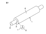
図1は、本発明の半導電性ローラの、実施の形態の一例を示す斜視図である。
図1を参照して、この例の半導電性ローラ1は、先に説明した各成分を含むゴム組成物によって筒状に形成され、中心の通孔2にシャフト3が挿通されて固定されるとともに、外周面4に紫外線照射によって酸化膜5が形成されたものである。
《Semiconductive roller》
FIG. 1 is a perspective view showing an example of an embodiment of a semiconductive roller of the present invention.
With reference to FIG. 1, the
シャフト3は、例えばアルミニウム、アルミニウム合金、ステンレス鋼等の金属によって一体に形成される。半導電性ローラ1とシャフト3とは、例えば導電性を有する接着剤等によって電気的に接合されるとともに機械的に固定されて一体に回転される。
かかる半導電性ローラ1は、例えばレーザープリンタ等の、電子写真法を利用した画像形成装置に組み込んで感光体の表面を一様に帯電させるための帯電ローラとして好適に使用できる。
The shaft 3 is integrally formed of a metal such as aluminum, an aluminum alloy, or stainless steel. The
The
半導電性ローラ1の径方向の厚みは、帯電ローラとして使用する場合、当該帯電ローラの小型化、軽量化を図りながら適度なニップ厚を確保するために0.5mm以上、特に1mm以上であるのが好ましく、15mm以下、中でも10mm以下、特に7mm以下であるのが好ましい。
半導電性ローラ1は、先に説明した各成分を含むゴム組成物を用いて、下記の工程を経て製造される。
When used as a charging roller, the radial thickness of the
The
すなわちゴム組成物を、押出成形機を用いて混練しながら加熱して溶融させた状態で、半導電性ローラ1の断面形状、すなわち円環状に対応するダイを通して長尺の筒状に押出成形する。
次いで冷却して固化させた筒体を所定の長さにカットし、通孔2に架橋用の仮のシャフトを挿通した状態で加硫缶内に収容し、当該加硫缶内に加熱水蒸気を供給して加熱、加圧することでゴム分を架橋させる。
That is, the rubber composition is extruded into a long cylindrical shape through a die corresponding to the cross-sectional shape of the
Next, the cooled and solidified cylindrical body is cut into a predetermined length, accommodated in a vulcanizing can with a temporary shaft for crosslinking inserted into the through hole 2, and heated steam is introduced into the vulcanizing can. By supplying, heating and pressurizing, the rubber component is crosslinked.
あるいは押出成形した筒体を長尺のまま送りながら連続架橋装置内を通過させて連続的に架橋させたのち所定の長さにカットする。
次いで外周面に導電性の接着剤を塗布したシャフト3を通孔2に挿通して、接着剤が熱硬化性接着剤である場合は加熱により硬化させて半導電性ローラ1とシャフト3とを電気的に接合するとともに機械的に固定する。
Alternatively, the extruded cylindrical body is passed through the continuous cross-linking apparatus while being sent in a long length, and is continuously cross-linked and then cut to a predetermined length.
Next, the shaft 3 having a conductive adhesive applied to the outer peripheral surface is inserted into the through hole 2, and when the adhesive is a thermosetting adhesive, the
そして必要に応じて半導電性ローラ1の両端をカットし、また外周面4を所定の表面粗さになるように研磨したのち紫外線を照射することで、当該外周面4を構成するゴム組成物中のNBRのジエン結合部分を酸化反応させて酸化膜5を生成させる。これにより図1に示す半導電性ローラ1が製造される。
かかる半導電性ローラ1は、先に説明した各成分を含有するゴム組成物からなり、しかも外周面4が酸化膜5で被覆されているため、先に説明したメカニズムにより、外周面の周方向や幅方向で電気抵抗値がばらついたりせず均一である。また感光体の汚染や外周面へのトナーの蓄積等よる画像不良が生じるおそれもない。しかも半導電性ローラ1は、上記ゴム組成物を用いることと、上記の工程を経ることとが相まって、従来に比べてコスト安価に製造することもできる。
And the rubber composition which comprises the said outer peripheral surface 4 is cut | disconnected as needed, both ends of the
Since the
なお半導電性ローラ1は、外周面4側の外層と、シャフト3側の内層の2層構造に形成してもよい。その場合、少なくとも外層を本発明の構成とすればよい。
また半導電性ローラ1は多孔質構造としてもよいが、耐摩耗性等を向上したり、先に説明したヘタリによるニップ跡の発生を防止したりすることを考慮すると非多孔質構造であるのが好ましい。
The
The
さらに半導電性ローラ1は、先に説明したようにローラ抵抗値が104Ω以上、106.5Ω未満である必要がある。ローラ抵抗値は、外周面4に酸化膜5を形成した状態での測定値である。
《ローラ抵抗値の測定方法》
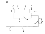
図2は、半導電性ローラ1のローラ抵抗値を測定する方法を説明する図である。
Furthermore, the
<Measurement method of roller resistance value>
FIG. 2 is a diagram for explaining a method of measuring the roller resistance value of the
図1、図2を参照して、本発明では半導電性ローラ1のローラ抵抗値を温度23℃、相対湿度55%の常温常湿環境下、印加電圧50Vの条件で、下記の方法によって測定した値でもって表すこととする。
すなわち一定の回転速度で回転させることができるアルミニウムドラム6を用意し、かかるアルミニウムドラム6の外周面7に、上方からローラ抵抗値を測定する半導電性ローラ1の、酸化膜5を形成した外周面4を接触させる。
With reference to FIGS. 1 and 2, in the present invention, the roller resistance value of the
In other words, an aluminum drum 6 that can be rotated at a constant rotational speed is prepared, and the outer periphery of the
また半導電性ローラ1のシャフト3とアルミニウムドラム6との間に直流電源8、および抵抗9を直列に接続して計測回路10を構成する。直流電源8は(−)側をシャフト3、(+)側を抵抗9と接続する。抵抗9の抵抗値rは100Ωとする。
次いでシャフト3の両端部にそれぞれ450gの荷重Fをかけて半導電性ローラ1をアルミニウムドラム6に圧接させた状態で、当該アルミニウムドラム6を回転(回転数:40rpm)させながら、両者間に直流電源8から直流50Vの印加電圧Eを印加した際に抵抗9にかかる検出電圧Vを計測する。
A
Next, while applying a load F of 450 g to both ends of the shaft 3 so that the
検出電圧Vと印加電圧E(=50V)とから、半導電性ローラ1のローラ抵抗値Rは、基本的に式(1′):
R=r×E/(V−r) (1′)
によって求められる。ただし式(1′)中の分母中の−rの項は微小とみなすことができるため、本発明では式(1):
R=r×E/V (1)
によって求めた値でもって半導電性ローラ1のローラ抵抗値とすることとする。測定の条件は、先に説明したように温度23℃、相対湿度55%である。
From the detection voltage V and the applied voltage E (= 50 V), the roller resistance value R of the
R = r × E / (V−r) (1 ′)
Sought by. However, since the −r term in the denominator in the formula (1 ′) can be regarded as minute, in the present invention, the formula (1):
R = r × E / V (1)
It is assumed that the roller resistance value of the
また半導電性ローラ1は、その用途等に応じて任意の硬さ、圧縮永久ひずみを有するように調整できる。かかる硬さ、圧縮永久ひずみ、並びにローラ抵抗値等を調整するためには、例えばNBRとEPDMの質量比(NBR)/(EPDM)を先に説明した範囲内で調整したり、架橋成分としての硫黄、過酸化物架橋剤、スルフェンアミド系促進剤等の種類と量を調整したり、カーボンブラックや充填剤その他の成分の種類と量を調整したりすればよい。
Moreover, the
本発明の半導電性ローラは帯電ローラのほか、例えば現像ローラ、転写ローラ、クリーニングローラ等としてレーザープリンタ、静電式複写機、普通紙ファクシミリ装置、あるいはこれらの複合機等の、電子写真法を利用した画像形成装置に用いることができる。 In addition to the charging roller, the semiconductive roller of the present invention can be applied to an electrophotographic method such as a developing roller, a transfer roller, a cleaning roller, a laser printer, an electrostatic copying machine, a plain paper facsimile machine, or a complex machine thereof. The image forming apparatus can be used.
〈実施例1〉
NBR〔低ニトリルNBR、アクリロニトリル含量:19.5%、非油展、JSR(株)製のJSR(登録商標)N250SL〕70質量部、およびEPDM〔エチレン含量:50%、ジエン含量:9.5%、非油展、住友化学(株)製のエスプレン(登録商標)505A〕30質量部をゴム分として、9Lニーダを用いて素練りしながら、下記表1に示す各成分を先に説明した手順で加えてさらに混練してゴム組成物を調製した。
<Example 1>
NBR (low nitrile NBR, acrylonitrile content: 19.5%, non-oil-extended, 70 parts by mass of JSR (registered trademark) N250SL manufactured by JSR Corporation), and EPDM (ethylene content: 50%, diene content: 9.5) %, Non-oil-extended, Esprene (registered trademark) 505A manufactured by Sumitomo Chemical Co., Ltd.] Each component shown in Table 1 below was first explained while masticating with 9 L kneader using 30 parts by mass of rubber. A rubber composition was prepared by adding in the procedure and further kneading.
NBRとEPDMの質量比(NBR)/(EPDM)=70/30であった。 The mass ratio of NBR to EPDM (NBR) / (EPDM) = 70/30.

表1中の各成分は下記のとおり。
ISAF:カーボンブラック〔東海カーボン(株)製のシースト6〕
粉末硫黄:架橋剤〔鶴見化学工業(株)製〕
促進剤CZ:N−シクロヘキシル−2−ベンゾチアゾリルスルフェンアミド〔大内新興化学工業(株)製のノクセラー(登録商標)CZ〕
過酸化物架橋剤:ジクミルパーオキサイド〔日油(株)製のパークミル(登録商標)D〕
酸化亜鉛2種:架橋助剤〔三井金属鉱業(株)製〕
表中の質量部は、先のゴム分の総量100質量部あたりの質量部である。
Each component in Table 1 is as follows.
ISAF: Carbon black [Seast 6 manufactured by Tokai Carbon Co., Ltd.]
Powdered sulfur: Cross-linking agent [manufactured by Tsurumi Chemical Co., Ltd.]
Accelerator CZ: N-cyclohexyl-2-benzothiazolylsulfenamide [Noxeller (registered trademark) CZ manufactured by Ouchi Shinsei Chemical Co., Ltd.]
Peroxide crosslinking agent: Dicumyl peroxide [Parkmill (registered trademark) D manufactured by NOF Corporation]
2 types of zinc oxide: Cross-linking aid [Mitsui Metal Mining Co., Ltd.]
The mass part in a table | surface is a mass part per 100 mass parts of total amounts of the previous rubber part.
次に、調製したゴム組成物をφ60の押出成形機に供給して外径φ11.0mm、内径φ5.5mmの筒状に押出成形した後、外径φ3mmの架橋用の仮のシャフトを挿通して加硫缶内で160℃×30分間加熱して架橋させた。
次いで、外周面に導電性の熱硬化性接着剤(ポリアミド系)を塗布した外径φ6mmの金属シャフトを挿通し直してオーブン中で150℃×60分間加熱して接着したのち両端をカットし、広幅研磨機を用いて外径がφ8.5mmになるまで外周面を研磨した。
Next, the prepared rubber composition is supplied to an extrusion molding machine having a diameter of 60 mm and extruded into a cylindrical shape having an outer diameter of 11.0 mm and an inner diameter of 5.5 mm, and then inserted through a temporary bridging shaft having an outer diameter of 3 mm. Then, it was crosslinked by heating in a vulcanizing can at 160 ° C. for 30 minutes.
Next, after inserting a metal shaft having an outer diameter of φ6 mm coated with a conductive thermosetting adhesive (polyamide type) on the outer peripheral surface and bonding it by heating at 150 ° C. for 60 minutes in an oven, both ends are cut, The outer peripheral surface was polished until the outer diameter became 8.5 mm using a wide polishing machine.
研磨後の外周面をアルコール拭きしたのち、UV光源から外周面までの距離を50mmとしてUV処理装置にセットし、30rpmで回転させながら紫外線を5分間照射することで酸化膜を形成して半導電性ローラを製造した。
〈実施例2、3、比較例1、2〉
NBRとEPDMの質量比(NBR)/(EPDM)を80/20(比較例1)、50/50(実施例2)、30/70(実施例3)、および20/80(比較例2)としたこと以外は実施例1と同様にしてゴム組成物を調製し、半導電性ローラを製造した。
After polishing the outer peripheral surface with alcohol, the distance from the UV light source to the outer peripheral surface is set to 50 mm, set in a UV processing apparatus, and irradiated with ultraviolet rays for 5 minutes while rotating at 30 rpm to form an oxide film to be semiconductive Sex rollers were manufactured.
<Examples 2 and 3, Comparative Examples 1 and 2>
The mass ratio (NBR) / (EPDM) of NBR and EPDM is 80/20 (Comparative Example 1), 50/50 (Example 2), 30/70 (Example 3), and 20/80 (Comparative Example 2). Except for the above, a rubber composition was prepared in the same manner as in Example 1 to produce a semiconductive roller.
〈比較例3〉
粉末硫黄と促進剤CZを配合しなかったこと以外は実施例1と同様にしてゴム組成物を調製し、半導電性ローラを製造した。NBRとEPDMの質量比(NBR)/(EPDM)=70/30であった。
〈比較例4〉
過酸化物架橋剤を配合しなかったこと以外は実施例1と同様にしてゴム組成物を調製し、半導電性ローラを製造した。NBRとEPDMの質量比(NBR)/(EPDM)=70/30であった。
<Comparative Example 3>
A rubber composition was prepared in the same manner as in Example 1 except that powdered sulfur and the accelerator CZ were not blended to produce a semiconductive roller. The mass ratio of NBR to EPDM (NBR) / (EPDM) = 70/30.
<Comparative example 4>
A rubber composition was prepared in the same manner as in Example 1 except that the peroxide crosslinking agent was not blended to produce a semiconductive roller. The mass ratio of NBR to EPDM (NBR) / (EPDM) = 70/30.
〈実施例4、5、比較例5、6〉
ISAFの配合割合を、ゴム分の総量100質量部あたり25質量部(比較例5)、27.5質量部(実施例4)、35質量部(実施例5)、および40質量部(比較例6)としたこと以外は実施例1と同様にしてゴム組成物を調製し、半導電性ローラを製造した。
〈実施例6、7、比較例7、8〉
ISAFに代えてSAF〔東海カーボン(株)製のシースト9〕を、ゴム分の総量100質量部あたり20質量部(比較例7)、22.5質量部(実施例6)、32.5質量部(実施例7)、および35質量部(比較例8)配合したこと以外は実施例1と同様にしてゴム組成物を調製し、半導電性ローラを製造した。
<Examples 4 and 5, Comparative Examples 5 and 6>
The blending ratio of ISAF was 25 parts by mass (Comparative Example 5), 27.5 parts by mass (Example 4), 35 parts by mass (Example 5), and 40 parts by mass (Comparative Example) per 100 parts by mass of rubber. A rubber composition was prepared in the same manner as in Example 1 except that 6), and a semiconductive roller was produced.
<Examples 6 and 7, Comparative Examples 7 and 8>
In place of ISAF, SAF [Shiest 9 manufactured by Tokai Carbon Co., Ltd.] was added in an amount of 20 parts by mass (Comparative Example 7), 22.5 parts by mass (Example 6), and 32.5 parts by mass per 100 parts by mass of rubber. A rubber composition was prepared in the same manner as in Example 1 except that 5 parts (Example 7) and 35 parts by mass (Comparative Example 8) were blended to produce a semiconductive roller.
〈実施例8、9、比較例9、10〉
ISAFに代えてHAF〔東海カーボン(株)製のシースト3〕を、ゴム分の総量100質量部あたり30質量部(比較例9)、32.5質量部(実施例8)、40質量部(実施例9)、および45質量部(比較例10)配合したこと以外は実施例1と同様にしてゴム組成物を調製し、半導電性ローラを製造した。
<Examples 8 and 9, Comparative Examples 9 and 10>
HAAF [Tokai Carbon Co., Ltd. Seast 3] was replaced with ISAF by 30 parts by mass (Comparative Example 9), 32.5 parts by mass (Example 8), 40 parts by mass (100 parts by mass of the total rubber content) A rubber composition was prepared in the same manner as in Example 1 except that Example 9) and 45 parts by mass (Comparative Example 10) were blended to produce a semiconductive roller.
〈比較例11〉
ISAFに代えてFEF〔東海カーボン(株)製のシーストSO〕を、ゴム分の総量100質量部あたり50質量部配合したこと以外は実施例1と同様にしてゴム組成物を調製し、半導電性ローラを製造した。
〈比較例12、13〉
ISAFに代えて導電性カーボンブラック〔電気化学工業(株)製のデンカ ブラック(登録商標)〕を、ゴム分の総量100質量部あたり20質量部(比較例12)、および30質量部(比較例13)配合したこと以外は実施例1と同様にしてゴム組成物を調製し、半導電性ローラを製造した。
<Comparative Example 11>
A rubber composition was prepared in the same manner as in Example 1 except that 50 parts by mass of FEF [Seat SO manufactured by Tokai Carbon Co., Ltd.] instead of ISAF was blended per 100 parts by mass of the total rubber content. Sex rollers were manufactured.
<Comparative Examples 12 and 13>
Instead of ISAF, conductive carbon black [DENKA BLACK (registered trademark) manufactured by Denki Kagaku Kogyo Co., Ltd.], 20 parts by mass (Comparative Example 12) and 30 parts by mass (Comparative Example) per 100 parts by mass of the total amount of rubber. 13) Except for blending, a rubber composition was prepared in the same manner as in Example 1 to produce a semiconductive roller.
〈加工性評価〉
架橋後に金属シャフトを挿通しなおす際に、スムースに挿通できたものを加工性良好「○」、挿通できなかったものを加工性不良「×」と評価した。
〈耐性評価〉
滋賀院照射によって外周面にクラックが発生したものを耐性不良「×」、発生しなかったものを耐性良好「○」と評価した。
<Processability evaluation>
When the metal shaft was reinserted after cross-linking, those that could be smoothly inserted were evaluated as “Good” for good workability, and those that could not be inserted were evaluated as “Good” for poor workability.
<Tolerance evaluation>
Those with cracks on the outer peripheral surface due to Shiga-in irradiation were evaluated as poor resistance “x”, and those without cracks were evaluated as good resistance “◯”.
〈ローラ抵抗値の測定〉
実施例、比較例で製造した半導電性ローラのローラ抵抗値を、温度23℃、相対湿度55%の常温常湿環境下、印加電圧50Vの条件で、先に説明した測定方法によって測定した。なお以下の表ではローラ抵抗値をlogR値で表している。
〈実機試験〉
感光体と、当該感光体の表面に常時接触させて配設された帯電ローラとを備え、レーザープリンタ本体に着脱自在とされたトナーカートリッジ〔キヤノン(株)製のCRG−316BLK〕の純正の帯電ローラに代えて、実施例、比較例で製造した半導電性ローラを帯電ローラとして組み込んだ。
<Roller resistance value measurement>
The roller resistance values of the semiconductive rollers manufactured in the examples and comparative examples were measured by the measurement method described above under the conditions of an applied voltage of 50 V under a normal temperature and humidity environment of a temperature of 23 ° C. and a relative humidity of 55%. In the following table, the roller resistance value is expressed as a logR value.
<Real machine test>
Genuine charging of a toner cartridge [CRG-316BLK manufactured by Canon Inc.], which includes a photosensitive member and a charging roller that is always in contact with the surface of the photosensitive member and is detachable from the laser printer body. Instead of the roller, a semiconductive roller manufactured in Examples and Comparative Examples was incorporated as a charging roller.
(初期画像評価)
そして組み立てたトナーカートリッジを、直後にカラーレーザープリンタ〔キヤノン(株)製のLBP5050〕に装填し、直ちにハーフトーン画像、ベタ画像を印刷して初期画像として評価した。
評価は、何らかの画像不良が見られたものを「×」、見られなかったものを「○」とした。
(Initial image evaluation)
The assembled toner cartridge was immediately loaded into a color laser printer [LBP5050 manufactured by Canon Inc.], and a halftone image and a solid image were immediately printed and evaluated as an initial image.
In the evaluation, “x” indicates that some image defect was observed, and “◯” indicates that no image defect was observed.
(通紙後画像評価)
また装填して500枚/日、1分間に2枚のペースでの通紙を5日間実施した後にハーフトーン画像、ベタ画像を各5枚ずつ連続印刷して、通紙後画像として評価した。
評価は、連続印刷の間に何らかの画像不良が見られたものを「×」、見られなかったものを「○」とした。
(Image evaluation after passing paper)
In addition, after loading, 500 sheets / day, passing two sheets per minute for 5 days, 5 halftone images and 5 solid images were continuously printed and evaluated as images after passing.
In the evaluation, “X” indicates that some kind of image defect was observed during continuous printing, and “◯” indicates that no image defect was observed.
(保管試験)
また別に用意した、組み立てた直後のトナーカートリッジを温度50℃、相対湿度90%の高温、高湿環境下で5日間静置したのち同じカラーレーザープリンタに装填してハーフトーン画像、ベタ画像を各5枚ずつ枚連続印刷する保管試験を実施した。
評価は、連続印刷中に1枚でも白スジの画像不良が見られたものを「×」、連続印刷の全枚数を通して白スジの画像不良が全く見られなかったものを「○」とした。
(Storage test)
Separately prepared toner cartridges immediately after assembly were allowed to stand for 5 days in a high humidity environment with a temperature of 50 ° C. and a relative humidity of 90%, and then loaded into the same color laser printer to display halftone images and solid images. A storage test was carried out in which 5 sheets were printed continuously.
The evaluation was “X” when even one sheet of white streak image defect was observed during continuous printing, and “◯” when no white streak image defect was observed throughout the continuous printing.
以上の結果を表2〜表5に示す。 The above results are shown in Tables 2 to 5.
表3の比較例1の結果より、ゴム分としてのNBRとEPDMの質量比(NBR)/(EPDM)が80/20でEPDMの量が不足する場合には耐性が不十分で、紫外線照射によって外周面にクラックが発生することが判った。そのため比較例1は特性を評価しなかった。
また比較例2の結果より、ゴム分としてのNBRとEPDMの質量比(NBR)/(EPDM)が20/80でNBRの量が不足する場合には、通紙後画像評価においてシリカ等の添加剤の蓄積による画像ムラが発生しているのが確認された。そしてこのことから、外周面に良好な酸化膜が形成されていないことが判った。
From the results of Comparative Example 1 in Table 3, when the mass ratio (NBR) / (EPDM) of NBR and EPDM as a rubber component is 80/20 and the amount of EPDM is insufficient, the resistance is insufficient, and UV irradiation causes It was found that cracks occurred on the outer peripheral surface. Therefore, Comparative Example 1 did not evaluate the characteristics.
Further, from the result of Comparative Example 2, when the mass ratio (NBR) / (EPDM) of NBR and EPDM as a rubber component is 20/80 and the amount of NBR is insufficient, silica or the like is added in the image evaluation after paper passing. It was confirmed that image unevenness due to accumulation of the agent occurred. From this, it was found that a good oxide film was not formed on the outer peripheral surface.
比較例3の結果より、架橋成分として過酸化物架橋剤のみを使用した場合には保管試験において画像不良が発生した。そこで状態を確認したところ、半導電性ローラが感光体に貼りついているのが確認され、ゴム分が架橋されていないことが判った。
表4の比較例4の結果より、架橋成分として硫黄とスルフェンアミド系促進剤のみを使用した場合には保管試験においてニップ跡の画像不良が発生した。そこで状態を観察したところ、保管時に感光体と接触し続けていた半導電性ローラの接触部位にヘタリが生じているのが確認され、ゴム分の架橋が十分でないことが判った。
From the result of Comparative Example 3, when only the peroxide crosslinking agent was used as the crosslinking component, an image defect occurred in the storage test. When the state was confirmed, it was confirmed that the semiconductive roller was stuck to the photoreceptor, and it was found that the rubber component was not crosslinked.
From the results of Comparative Example 4 in Table 4, when only sulfur and a sulfenamide accelerator were used as the crosslinking component, an image defect of the nip mark occurred in the storage test. When the state was observed, it was confirmed that the semiconductive roller was kept in contact with the photosensitive member at the time of storage, and it was confirmed that the rubber was not sufficiently crosslinked.
表5の比較例11の結果より、カーボンブラックとしてFEFを使用するとともに、半導電性ローラのローラ抵抗値を下げるために配合割合をゴム分の総量100質量部あたり50質量部とした場合には架橋後に硬くなりすぎて、金属シャフトをスムースに挿通できないことが判った。
また比較例12、13の結果より、カーボンブラックとして導電性カーボンブラックを使用した場合には、当該導電性カーボンブラックの分散性が低いため、酸化膜では十分にカバーできない電気抵抗値のばらつきを生じて感光体の表面を均一に帯電させることができず、形成画像に濃度ムラ等の画像不良を生じることが判った。
From the results of Comparative Example 11 in Table 5, when FEF was used as carbon black and the blending ratio was 50 parts by mass per 100 parts by mass of the total rubber content in order to reduce the roller resistance value of the semiconductive roller, It turned out that it became too hard after cross-linking and the metal shaft could not be smoothly inserted.
Further, from the results of Comparative Examples 12 and 13, when conductive carbon black is used as the carbon black, the dispersion of the conductive carbon black is low, resulting in variations in electrical resistance values that cannot be sufficiently covered by the oxide film. As a result, it was found that the surface of the photoconductor could not be uniformly charged, and an image defect such as density unevenness occurred in the formed image.
これに対し実施例1〜9の結果より、ゴム分としてのNBRとEPDMの質量比(NBR)/(EPDM)を70/30〜30/70の範囲とし、カーボンブラックとしてSAF、ISAF、およびHAFからなる群より選ばれた少なくとも1種を使用するとともに、架橋成分として硫黄、過酸化物架橋剤、およびスルフェンアミド系促進剤の3種を併用することで上記の問題をいずれも解消して、外周面の周方向や幅方向で電気抵抗値がばらついたりせず均一な半導電性ローラを、従来に比べてコスト安価に製造できることが判った。 On the other hand, from the results of Examples 1 to 9, the mass ratio (NBR) / (EPDM) of NBR and EPDM as a rubber component is in the range of 70/30 to 30/70, and SAF, ISAF, and HAF are used as carbon black. In addition to using at least one selected from the group consisting of: sulfur, a peroxide cross-linking agent, and a sulfenamide accelerator in combination as a cross-linking component, all of the above problems can be solved. It has been found that a uniform semi-conductive roller can be produced at a lower cost than the conventional one without variation in electric resistance value in the circumferential direction and width direction of the outer peripheral surface.
ただし実施例1、4、5、比較例5、6の結果より、カーボンブラックとしてISAFを使用した系では、ローラ抵抗値を104Ω以上、106.5Ω以下の範囲として良好な画像を形成するために、当該ISAFの配合割合を、ゴム分の総量100質量部あたり27.5質量部以上に設定するのが好ましく、35質量部以下に設定するのが好ましいことが判った。 However, from the results of Examples 1, 4, 5 and Comparative Examples 5 and 6, in the system using ISAF as the carbon black, the roller resistance value is in the range of 10 4 Ω to 10 6.5 Ω, and a good image is obtained. In order to form it, it turned out that it is preferable to set the mixing | blending ratio of the said ISAF to 27.5 mass parts or more per 100 mass parts of rubber | gum total amount, and to set to 35 mass parts or less.
また実施例6、7、比較例7、8の結果より、カーボンブラックとしてSAFを使用した系では、ローラ抵抗値を上記の範囲として良好な画像を形成するために、当該SAFの配合割合を、ゴム分の総量100質量部あたり22.5質量部以上に設定するのが好ましく、32.5質量部以下に設定するのが好ましいことが判った。
さらに実施例8、9、比較例9、10の結果より、カーボンブラックとしてHAFを使用した系では、ローラ抵抗値を上記の範囲として良好な画像を形成するために、当該HAFの配合割合を、ゴム分の総量100質量部あたり32.5質量部以上に設定するのが好ましく、40質量部以下に設定するのが好ましいことが判った。
Further, from the results of Examples 6 and 7 and Comparative Examples 7 and 8, in the system using SAF as carbon black, in order to form a good image with the roller resistance value in the above range, the blending ratio of the SAF is It was found that it is preferably set to 22.5 parts by mass or more per 100 parts by mass of the total amount of rubber, and preferably set to 32.5 parts by mass or less.
Further, from the results of Examples 8 and 9 and Comparative Examples 9 and 10, in the system using HAF as carbon black, in order to form a good image with the roller resistance value in the above range, the blending ratio of the HAF is It has been found that it is preferably set to 32.5 parts by mass or more per 100 parts by mass of the total amount of rubber, and preferably set to 40 parts by mass or less.
1 半導電性ローラ
2 通孔
3 シャフト
4 外周面
5 酸化膜
6 アルミニウムドラム
7 外周面
8 直流電源
9 抵抗
10 計測回路
F 荷重
V 検出電圧
DESCRIPTION OF
Claims (4)
前記ゴム分の総量100質量部あたり50質量部未満の範囲で、かつローラ抵抗値が104Ω以上、106.5Ω以下となるように配合割合が調整されたSAF、ISAF、およびHAFからなる群より選ばれた少なくとも1種のカーボンブラック、ならびに
前記ゴム分を架橋させるための架橋成分としての硫黄、過酸化物架橋剤、およびスルフェンアミド系促進剤を含むゴム組成物を筒状に押出成形し、
加硫缶または連続架橋装置を用いて架橋させたのちシャフトを挿通した状態で、
紫外線の照射により外周面に酸化膜を形成してなる半導電性ローラ。 A rubber component containing only two types of acrylonitrile butadiene rubber (NBR) and ethylene propylene diene rubber (EPDM) in a mass ratio (NBR) / (EPDM) = 70/30 to 30/70,
From SAF, ISAF, and HAF in which the blending ratio is adjusted so that the total amount of the rubber is less than 50 parts by mass per 100 parts by mass and the roller resistance value is 10 4 Ω or more and 10 6.5 Ω or less. And a rubber composition comprising at least one carbon black selected from the group consisting of sulfur as a crosslinking component for crosslinking the rubber component, a peroxide crosslinking agent, and a sulfenamide accelerator. Extruded,
After cross-linking using a vulcanizing can or continuous cross-linking device, with the shaft inserted,
A semiconductive roller formed by forming an oxide film on the outer peripheral surface by irradiation with ultraviolet rays.
Priority Applications (3)
| Application Number | Priority Date | Filing Date | Title |
|---|---|---|---|
| JP2014094656A JP5936282B2 (en) | 2014-05-01 | 2014-05-01 | Semi-conductive roller |
| CN201510212303.4A CN105017579B (en) | 2014-05-01 | 2015-04-29 | Semi-conductive roller |
| US14/700,604 US9539744B2 (en) | 2014-05-01 | 2015-04-30 | Semiconductive roller and production method therefor |
Applications Claiming Priority (1)
| Application Number | Priority Date | Filing Date | Title |
|---|---|---|---|
| JP2014094656A JP5936282B2 (en) | 2014-05-01 | 2014-05-01 | Semi-conductive roller |
Publications (2)
| Publication Number | Publication Date |
|---|---|
| JP2015212728A JP2015212728A (en) | 2015-11-26 |
| JP5936282B2 true JP5936282B2 (en) | 2016-06-22 |
Family
ID=54355175
Family Applications (1)
| Application Number | Title | Priority Date | Filing Date |
|---|---|---|---|
| JP2014094656A Active JP5936282B2 (en) | 2014-05-01 | 2014-05-01 | Semi-conductive roller |
Country Status (3)
| Country | Link |
|---|---|
| US (1) | US9539744B2 (en) |
| JP (1) | JP5936282B2 (en) |
| CN (1) | CN105017579B (en) |
Families Citing this family (8)
| Publication number | Priority date | Publication date | Assignee | Title |
|---|---|---|---|---|
| JP5009406B2 (en) * | 2010-05-12 | 2012-08-22 | 住友ゴム工業株式会社 | Charging roller |
| JP6140505B2 (en) * | 2013-03-29 | 2017-05-31 | 住友ゴム工業株式会社 | Rubber composition, paper feed roller, and image forming apparatus |
| CN108508723A (en) * | 2018-03-02 | 2018-09-07 | 郴州市展信龙科技有限公司 | A kind of production technology of environment protection-type developer roll |
| CN108445722A (en) * | 2018-03-02 | 2018-08-24 | 郴州市展信龙科技有限公司 | A kind of environment protection-type developer roll |
| CN112662028A (en) * | 2020-12-24 | 2021-04-16 | 中国化工集团曙光橡胶工业研究设计院有限公司 | Heat-aging-resistant nitrile rubber and preparation method thereof |
| JP2022168615A (en) * | 2021-04-26 | 2022-11-08 | 住友ゴム工業株式会社 | electrophotographic conductive roller |
| JP7772663B2 (en) * | 2022-06-24 | 2025-11-18 | 住友理工株式会社 | Charging rolls for electrophotographic equipment |
| CN117912854B (en) * | 2024-03-19 | 2024-06-28 | 深圳新宙邦科技股份有限公司 | Capacitor packaging material, preparation method thereof and capacitor |
Family Cites Families (25)
| Publication number | Priority date | Publication date | Assignee | Title |
|---|---|---|---|---|
| JP3449726B2 (en) | 1995-07-11 | 2003-09-22 | 日本ゼオン株式会社 | Conductive rubber composition and method for producing the same |
| JPH1144317A (en) * | 1997-07-29 | 1999-02-16 | Sumitomo Rubber Ind Ltd | Conductive foamed rubber tube, method for producing the same, and conductive elastic roller |
| JP3951860B2 (en) * | 2001-08-28 | 2007-08-01 | 東海ゴム工業株式会社 | Semiconductive polymer elastic member for semiconductive member of electrophotographic apparatus, semiconductive member using the same, and method for producing semiconductive polymer elastic member for semiconductive member of electrophotographic apparatus |
| JP4221186B2 (en) * | 2002-03-28 | 2009-02-12 | 住友ゴム工業株式会社 | Transfer roller |
| KR100592928B1 (en) | 2002-11-13 | 2006-06-23 | 스미토모 고무 고교 가부시키가이샤 | A conductive elastomer composition, a conductive member using the composition, and an image forming apparatus provided with the conductive member |
| KR100996727B1 (en) | 2002-11-15 | 2010-11-25 | 스미토모 고무 고교 가부시키가이샤 | An image forming apparatus having a conductive roller and the conductive roller |
| JP4221211B2 (en) * | 2002-11-15 | 2009-02-12 | 住友ゴム工業株式会社 | Conductive roller and image forming apparatus provided with the conductive roller |
| JP2006016552A (en) * | 2004-07-02 | 2006-01-19 | Sumitomo Rubber Ind Ltd | Rubber composition and paper feed roller |
| JP5158738B2 (en) * | 2005-09-30 | 2013-03-06 | シンジーテック株式会社 | Foam rubber roll and method for producing foam rubber roll |
| JP4116043B2 (en) * | 2006-04-14 | 2008-07-09 | 住友ゴム工業株式会社 | Rubber roller for image forming device |
| JP5188681B2 (en) * | 2006-04-14 | 2013-04-24 | 住友ゴム工業株式会社 | Semiconductive rubber member and developing roller comprising the rubber member |
| JP2007283659A (en) * | 2006-04-18 | 2007-11-01 | Canon Chemicals Inc | Apparatus and method for manufacturing conductive rubber roller, and roller and transfer roller for electrophotographic device |
| JP5021354B2 (en) * | 2006-04-28 | 2012-09-05 | 住友ゴム工業株式会社 | Rubber member and developing roller comprising the rubber member |
| JP4700746B2 (en) * | 2009-04-21 | 2011-06-15 | 住友ゴム工業株式会社 | Conductive roller |
| JP2011048188A (en) * | 2009-08-27 | 2011-03-10 | Sumitomo Rubber Ind Ltd | Conductive roller and electrophotographic device using the same |
| JP5009406B2 (en) | 2010-05-12 | 2012-08-22 | 住友ゴム工業株式会社 | Charging roller |
| JP5081292B2 (en) * | 2010-11-18 | 2012-11-28 | 住友ゴム工業株式会社 | Transfer member |
| CN102156399B (en) * | 2011-01-28 | 2012-07-25 | 刘宝利 | Production method of conductive rubber sponge transfer roller, and sponge composite |
| JP5236757B2 (en) * | 2011-02-07 | 2013-07-17 | 住友ゴム工業株式会社 | Semi-conductive roller |
| JP5736888B2 (en) * | 2011-03-25 | 2015-06-17 | 富士ゼロックス株式会社 | Roll member, charging device, process cartridge, and image forming apparatus |
| JP2013117678A (en) * | 2011-12-05 | 2013-06-13 | Sumitomo Rubber Ind Ltd | Semiconductive roller |
| CN103242571B (en) * | 2012-02-02 | 2016-08-03 | 住友橡胶工业株式会社 | Conductive rubber composition and use its transfer roll |
| JP5386025B1 (en) * | 2012-09-06 | 2014-01-15 | ヤマウチ株式会社 | Conductive rubber roller composition and conductive rubber roller |
| JP2014085479A (en) * | 2012-10-23 | 2014-05-12 | Sumitomo Rubber Ind Ltd | Semiconductive roller |
| KR20150034515A (en) * | 2013-09-26 | 2015-04-03 | 삼성전자주식회사 | Semiconductive roller for image forming apparatus |
-
2014
- 2014-05-01 JP JP2014094656A patent/JP5936282B2/en active Active
-
2015
- 2015-04-29 CN CN201510212303.4A patent/CN105017579B/en active Active
- 2015-04-30 US US14/700,604 patent/US9539744B2/en active Active
Also Published As
| Publication number | Publication date |
|---|---|
| CN105017579A (en) | 2015-11-04 |
| US20150316869A1 (en) | 2015-11-05 |
| JP2015212728A (en) | 2015-11-26 |
| CN105017579B (en) | 2018-05-18 |
| US9539744B2 (en) | 2017-01-10 |
Similar Documents
| Publication | Publication Date | Title |
|---|---|---|
| JP5936282B2 (en) | Semi-conductive roller | |
| JP3639773B2 (en) | Semiconductive rubber composition, charging member, electrophotographic apparatus, process cartridge | |
| JP3449726B2 (en) | Conductive rubber composition and method for producing the same | |
| JP5009406B2 (en) | Charging roller | |
| JPWO1997003122A1 (en) | Conductive rubber composition and method for producing the same | |
| JP6764568B2 (en) | Semi-conductive roller | |
| JP5086418B2 (en) | Method for manufacturing semiconductive roller | |
| CN1189796C (en) | Conducting rubber roller | |
| WO2016158813A1 (en) | Electrophotographic equipment-use electrically conductive member | |
| JP2008256908A (en) | Conductive rubber roller for electrifying member | |
| JP2009031574A (en) | Conductive rubber roller, transfer roller and image forming apparatus | |
| US10199134B2 (en) | Electrically conductive rubber composition, and developing roller | |
| JP2009122592A (en) | Conductive rubber roller | |
| JP3820764B2 (en) | Transfer belt member | |
| CN105637033B (en) | Conductive elastomer composition and its preparation method | |
| JP2011138004A (en) | Conductive roller for electrophotography and charging roller using the same | |
| JP3656904B2 (en) | Conductive rubber roller | |
| JP2016206457A (en) | Semiconductive roller | |
| JP2022168615A (en) | electrophotographic conductive roller | |
| JP2008299120A (en) | Charging member | |
| JP2004263059A (en) | Conductive rubber roller | |
| JP4886864B2 (en) | Non-halogen conductive roller | |
| JP3886722B2 (en) | Conductive polymer elastic composition | |
| JP7396135B2 (en) | Conductive roller for electrophotography | |
| JP2004059691A (en) | Conductive rubber composition |
Legal Events
| Date | Code | Title | Description |
|---|---|---|---|
| TRDD | Decision of grant or rejection written | ||
| A01 | Written decision to grant a patent or to grant a registration (utility model) |
Free format text: JAPANESE INTERMEDIATE CODE: A01 Effective date: 20160414 |
|
| A61 | First payment of annual fees (during grant procedure) |
Free format text: JAPANESE INTERMEDIATE CODE: A61 Effective date: 20160509 |
|
| R150 | Certificate of patent or registration of utility model |
Ref document number: 5936282 Country of ref document: JP Free format text: JAPANESE INTERMEDIATE CODE: R150 |
|
| R250 | Receipt of annual fees |
Free format text: JAPANESE INTERMEDIATE CODE: R250 |
|
| R250 | Receipt of annual fees |
Free format text: JAPANESE INTERMEDIATE CODE: R250 |
|
| R250 | Receipt of annual fees |
Free format text: JAPANESE INTERMEDIATE CODE: R250 |
|
| R250 | Receipt of annual fees |
Free format text: JAPANESE INTERMEDIATE CODE: R250 |
|
| R250 | Receipt of annual fees |
Free format text: JAPANESE INTERMEDIATE CODE: R250 |
|
| R250 | Receipt of annual fees |
Free format text: JAPANESE INTERMEDIATE CODE: R250 |
|
| R250 | Receipt of annual fees |
Free format text: JAPANESE INTERMEDIATE CODE: R250 |
|
| R250 | Receipt of annual fees |
Free format text: JAPANESE INTERMEDIATE CODE: R250 |