JP5932261B2 - Memory control device and memory control method - Google Patents
Memory control device and memory control method Download PDFInfo
- Publication number
- JP5932261B2 JP5932261B2 JP2011161055A JP2011161055A JP5932261B2 JP 5932261 B2 JP5932261 B2 JP 5932261B2 JP 2011161055 A JP2011161055 A JP 2011161055A JP 2011161055 A JP2011161055 A JP 2011161055A JP 5932261 B2 JP5932261 B2 JP 5932261B2
- Authority
- JP
- Japan
- Prior art keywords
- memory
- power saving
- access request
- saving state
- memory access
- Prior art date
- Legal status (The legal status is an assumption and is not a legal conclusion. Google has not performed a legal analysis and makes no representation as to the accuracy of the status listed.)
- Expired - Fee Related
Links
Images

Classifications
-
- G—PHYSICS
- G06—COMPUTING; CALCULATING OR COUNTING
- G06F—ELECTRIC DIGITAL DATA PROCESSING
- G06F1/00—Details not covered by groups G06F3/00 - G06F13/00 and G06F21/00
- G06F1/26—Power supply means, e.g. regulation thereof
- G06F1/32—Means for saving power
- G06F1/3203—Power management, i.e. event-based initiation of a power-saving mode
- G06F1/3206—Monitoring of events, devices or parameters that trigger a change in power modality
- G06F1/3215—Monitoring of peripheral devices
- G06F1/3225—Monitoring of peripheral devices of memory devices
-
- G—PHYSICS
- G06—COMPUTING; CALCULATING OR COUNTING
- G06F—ELECTRIC DIGITAL DATA PROCESSING
- G06F1/00—Details not covered by groups G06F3/00 - G06F13/00 and G06F21/00
- G06F1/26—Power supply means, e.g. regulation thereof
- G06F1/32—Means for saving power
- G06F1/3203—Power management, i.e. event-based initiation of a power-saving mode
- G06F1/3234—Power saving characterised by the action undertaken
- G06F1/325—Power saving in peripheral device
- G06F1/3275—Power saving in memory, e.g. RAM, cache
-
- G—PHYSICS
- G06—COMPUTING; CALCULATING OR COUNTING
- G06F—ELECTRIC DIGITAL DATA PROCESSING
- G06F13/00—Interconnection of, or transfer of information or other signals between, memories, input/output devices or central processing units
- G06F13/14—Handling requests for interconnection or transfer
- G06F13/16—Handling requests for interconnection or transfer for access to memory bus
- G06F13/1605—Handling requests for interconnection or transfer for access to memory bus based on arbitration
- G06F13/161—Handling requests for interconnection or transfer for access to memory bus based on arbitration with latency improvement
- G06F13/1626—Handling requests for interconnection or transfer for access to memory bus based on arbitration with latency improvement by reordering requests
-
- Y—GENERAL TAGGING OF NEW TECHNOLOGICAL DEVELOPMENTS; GENERAL TAGGING OF CROSS-SECTIONAL TECHNOLOGIES SPANNING OVER SEVERAL SECTIONS OF THE IPC; TECHNICAL SUBJECTS COVERED BY FORMER USPC CROSS-REFERENCE ART COLLECTIONS [XRACs] AND DIGESTS
- Y02—TECHNOLOGIES OR APPLICATIONS FOR MITIGATION OR ADAPTATION AGAINST CLIMATE CHANGE
- Y02D—CLIMATE CHANGE MITIGATION TECHNOLOGIES IN INFORMATION AND COMMUNICATION TECHNOLOGIES [ICT], I.E. INFORMATION AND COMMUNICATION TECHNOLOGIES AIMING AT THE REDUCTION OF THEIR OWN ENERGY USE
- Y02D10/00—Energy efficient computing, e.g. low power processors, power management or thermal management
Description
本発明は複数のマスタと複数のメモリに接続されたメモリ制御装置に関し、特にメモリアクセスが競合した場合にメモリアクセスの優先順位を制御するメモリ制御装置、メモリ制御方法に関する。 The present invention relates to a memory control device connected to a plurality of masters and a plurality of memories, and more particularly to a memory control device and a memory control method for controlling the priority of memory access when memory accesses compete.
近年のLSIはチップ上にCPU以外にも多数のIP(information processor)を搭載し高機能化が進んでいる。このようなシステムにおいては、個々のIPが同時にデータ処理を行うため、大容量で高速なメモリを、LSIと同時にシステム基板上に搭載するシステムも増えている。 In recent years, LSIs are equipped with many information processors (IPs) in addition to CPUs on chips, and their functions have been advanced. In such a system, since individual IPs simultaneously process data, an increasing number of systems have a large-capacity and high-speed memory mounted on a system board simultaneously with an LSI.
例えば、SDRAMデバイスがメモリデバイスとして用いられていたが、昨今ではさらに高速アクセスのためにDDR−SDRAMあるいはDDR2−SDRAM、DDR3−SDRAMといった高速なメモリデバイスが複数個用いられることがある。 For example, an SDRAM device has been used as a memory device. Recently, however, a plurality of high-speed memory devices such as DDR-SDRAM, DDR2-SDRAM, and DDR3-SDRAM may be used for higher-speed access.
一方で、バッテリー駆動を前提とするシステムを中心に、システム全体の消費電力を下げる様々な取り組みが行われている。例えば、メモリデバイスにおいては、低消費電力モードが設けられ、メモリアクセスを行わない場合に、メモリを低消費電力モードに移行させることで、メモリデバイスの消費電力を下げることが可能となっている。 On the other hand, various efforts are being made to reduce the power consumption of the entire system, with a focus on systems that are battery driven. For example, in a memory device, when a low power consumption mode is provided and memory access is not performed, the power consumption of the memory device can be reduced by shifting the memory to the low power consumption mode.
メモリ制御装置としては、メモリを低消費電力モードにさせる期間を長くさせるようにメモリアクセスを制御することが省電力のために必要となる。 As a memory control device, it is necessary for power saving to control memory access so as to lengthen the period during which the memory is in the low power consumption mode.
例えば特許文献1は、メモリ(スレーブ)の状態を監視してメモリアクセスの優先順位を切替える必要があるが、メモリ(スレーブ)の状態を監視して複数バスマスタの転送要求の優先順位を切替える方法を開示している。特許文献1では、スレーブがバスマスタの転送要求を直ちに処理できる状態にあるかを判断し、直ちに処理できない状態にあると判断されたスレーブに対する転送要求をマスクして、直ちに処理できる状態にあると判断されたスレーブに対する転送要求のなかから転送を受け付ける処理を行っている。
For example,
システム内のスレーブモジュールの一つとしてチップ外部に接続されるDRAM等のメモリ制御装置が存在する。DRAMのメモリ制御装置はバスマスタからのメモリアクセスを接続されるDRAMのプロトコルに変換しメモリアクセスを発行する機能を有する。またメモリ制御装置は外部のDRAMの電力モードを制御する機能を有するものも存在する。外部DRAMの電力モードを制御する機能を有したメモリ制御回路の実装の形態として、システムから明示的に電力モードの指定を受け、パワーダウンやセルフリフレッシュの投入・復帰といった電力モード制御用のコマンドを発行するものがある。 As one of the slave modules in the system, there is a memory control device such as a DRAM connected to the outside of the chip. A DRAM memory control device has a function of issuing a memory access by converting a memory access from a bus master into a protocol of a connected DRAM. Some memory control devices have a function of controlling the power mode of an external DRAM. As a form of implementation of the memory control circuit with the function to control the power mode of the external DRAM, a command for power mode control such as power-down and self-refresh on / return is received from the system explicitly. There is something to issue.
この場合、システムからの明示的な指定があるため、極め細やかな制御が困難であった。一方で、バスマスタからのメモリアクセスの受け付け状態により、自動的に電源モードの制御を行う機能を有するものもある。すなわち、バスマスタからの転送要求がない場合、メモリを省電力モードに投入し、省電力モードに投入されたメモリに転送要求があると、メモリを省電力モードから通常のメモリアクセスが可能な状態へ復帰させるような機能を有する。 In this case, since there is an explicit designation from the system, extremely fine control is difficult. On the other hand, some have a function of automatically controlling the power mode depending on the memory access acceptance state from the bus master. In other words, when there is no transfer request from the bus master, the memory is put into the power saving mode, and when there is a transfer request to the memory put into the power saving mode, the memory is changed from the power saving mode to a state where normal memory access is possible. It has a function of returning.
従来の調停方法は、スレーブの状態が、直ちに使用できない状態から直ちに使用できる状態へと自動的に切り替わることを前提に行われている。 The conventional arbitration method is performed on the premise that the slave state automatically switches from a state where it cannot be used immediately to a state where it can be used immediately.
このようなメモリ制御装置において、「スレーブがバスマスタの転送要求を直ちに処理できない状態」を「メモリが省電力モードに投入された状態」と置き換えた場合、省電力モードに投入されたメモリへのアクセスがマスクされる。すなわち、省電力モードからの復帰することでメモリアクセス発行可能であるにも関わらず、メモリアクセスがマスクされることとなる。 In such a memory control device, when “the state where the slave cannot process the bus master transfer request immediately” is replaced with “the state where the memory is put into the power saving mode”, the access to the memory put into the power saving mode is performed. Is masked. That is, the memory access is masked even though the memory access can be issued by returning from the power saving mode.
なお、省電力モードに投入されたメモリデバイスへのアクセスがマスクされると、省電力モードにあるメモリは、省電力モード状態にとどまり続けるためメモリ転送が行われない。 Note that if access to the memory device put into the power saving mode is masked, the memory in the power saving mode remains in the power saving mode and memory transfer is not performed.
一方、メモリが省電力モードに投入された状態を、スレーブがバスマスタ要求を直ちに処理できる状態とした場合、省電力モードに投入されたメモリデバイスへのメモリアクセスはマスクされない。しかしながら、メモリアクセスの発行順序に依存し、省電力モードに投入される期間が短くなり、省電力効果が少なくなる。 On the other hand, when the state where the memory is put into the power saving mode is changed to a state where the slave can process the bus master request immediately, the memory access to the memory device put into the power saving mode is not masked. However, depending on the memory access issuance order, the period for entering the power saving mode is shortened, and the power saving effect is reduced.
以上の問題を鑑みて、本発明は省電力モードを有するメモリ制御回路におけるメモリアクセスと省電力の効率を向上させるメモリ制御装置、メモリ制御方法を提供することを目的とする。 In view of the above problems, an object of the present invention is to provide a memory control device and a memory control method that improve the efficiency of memory access and power saving in a memory control circuit having a power saving mode.
上記課題を解決するために本発明に係るメモリ制御装置は、複数のマスタと省電力状態に遷移可能な複数のメモリとの間に接続されたメモリ制御装置であって、前記複数のマスタからのメモリアクセス要求を調停し、前記複数のマスタの1つにメモリアクセス要求を許可する調停手段と、前記複数のメモリのそれぞれが省電力状態にあるか否かを監視する監視手段とを有し、前記調停手段は、前記監視手段の検出結果に応じて、省電力状態にあるメモリに対するメモリアクセス要求と省電力状態にないメモリに対するメモリアクセス要求が競合する場合、省電力状態にないメモリに対するメモリアクセス要求から優先的に選択している間に、省電力状態にあるメモリに対するメモリアクセス要求が所定回数以上、受け付けられなかった場合に、省電力状態にあるメモリへのメモリアクセス要求を選択対象に含めることを特徴とする。 In order to solve the above-described problem, a memory control device according to the present invention is a memory control device connected between a plurality of masters and a plurality of memories capable of transitioning to a power saving state. Arbitrating means for arbitrating a memory access request and allowing the memory access request to one of the plurality of masters; and monitoring means for monitoring whether each of the plurality of memories is in a power saving state; The arbitration unit, when a memory access request for a memory in a power saving state and a memory access request for a memory not in a power saving state compete with each other according to a detection result of the monitoring unit, while preferentially selected from the request, the memory access request to the memory in a power saving state a predetermined number of times or more, if not accepted Included in the selected target memory access request to the memory in a power saving state, characterized in Rukoto.
本発明によれば、省電力モードに投入されたメモリに対するアクセスの処理優先度を下げる、省電力モードの時間を長くすることでシステム全体における消費電力の低減が可能となる。 According to the present invention, it is possible to reduce power consumption in the entire system by lowering the processing priority of access to a memory put into the power saving mode and lengthening the time in the power saving mode.
(第1の実施形態)
以下、図1、図2に基づき、本発明の一実施形態である第1の実施形態のメモリ制御装置(以下、メモリ制御回路と称す)について説明する。図1は実施形態1のメモリ制御回路の概略構成を示すブロック図である。
(First embodiment)
Hereinafter, a memory control device (hereinafter referred to as a memory control circuit) according to a first embodiment which is an embodiment of the present invention will be described with reference to FIGS. FIG. 1 is a block diagram illustrating a schematic configuration of the memory control circuit according to the first embodiment.
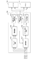
図1において省電力モード(省電力状態)に遷移可能な複数のメモリ110、111がメモリ制御回路100によってアクセスされる構成になっている。省電力モード制御回路101はメモリ110、111に接続されこれらのメモリを省電力モード(省電力状態)へ投入、または解除をする。省電力モード監視回路102は省電力モード制御回路101によりメモリ110、111が省電力モードに投入されているか監視する。アクセス保持回路103はメモリアクセスコマンド(以下、単にアクセス)を複数保持する。
In FIG. 1, a plurality of
メモリコマンド生成回路104はメモリ110と111に接続されアクセス保持回路103の先頭に登録されているアクセスを取り出し、メモリ110、111(例えば、SDRAM、DDR−SDRAM、DDR2〜4−SDRAM)へアクセスするためのコマンドに変換し発行する。デコード回路105は外部からのアクセスがメモリ110、111のどちらに対するものかアドレスをデコードする。調停回路106はデコード回路105のデコード結果と省電力モード監視回路102の情報(検出結果)から複数のメモリアクセス要求のうちアクセスを許可するバスマスタモジュール(以下、バスマスタと称す)を決定する。選択回路107は、調停回路106で決定されたアクセスを選択してアクセス保持回路103に登録する。
The memory
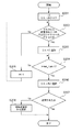
図2は図1に示す調停回路106がバスマスタからのアクセス要求のどれを選択するかを決定する処理のフローチャートである。調停回路106はバスマスタからの転送要求が発生すると、調停動作を開始する。まず、内部変数iと省電力モードではないメモリに対するアクセス要求を集計するためのリストをクリアする(S201)。
FIG. 2 is a flowchart of a process for determining which access request from the bus master is to be selected by the
次に、アクセス要求があり、かつ、アクセス要求されているメモリが省電力モードに投入中ではないメモリに対するアクセス要求を発行しているバスマスタについてバスマスタ0から順にバスマスタ番号をリストに登録する(S202)。
Next, the bus master numbers are registered in order from the
全てのバスマスタのアクセス要求に対するリスト集計作業が終了したら、リストに登録されているバスマスタの中から、アクセスを許可するバスマスタを選択する。バスマスタの選択方法としては、固定優先順位方式や、ラウンドロビン方式など、既存の調停アルゴリズムによる選択を行うことが可能である。 When the list totaling operation for all bus master access requests is completed, a bus master to which access is permitted is selected from the bus masters registered in the list. As a method of selecting a bus master, it is possible to perform selection using an existing arbitration algorithm such as a fixed priority method or a round robin method.
リストに登録されたバスマスタが選択された場合は、そのまま終了するが、リストにどのバスマスタも登録されない場合は、リスト以外のバスマスタも含めて、再度アクセスを許可するバスマスタを選択する。 When a bus master registered in the list is selected, the process is terminated as it is. However, when no bus master is registered in the list, a bus master that permits access again including a bus master other than the list is selected.
上記動作により、省電力モードに投入されているメモリに対するアクセス要求と、省電力モードに投入されていないメモリに対するアクセス要求が競合した場合に、省電力モードに投入されていないメモリに対するアクセス要求が優先的に選択される。そのため、省電力モードに投入されているメモリに対するアクセス要求が待たされることで、省電力モードに投入されているメモリは、長時間、省電力モードに投入された状態を保持することが可能となる。さらに、省電力モードから復帰したメモリに対してアクセス要求がまとまって実行されるように制御できるので、省電力モードと通常モードとの間を遷移する回数を低減させ、メモリの状態遷移に要する時間と状態遷移によって消費される消費電力を低減することができる。 With the above operation, when an access request to a memory that has not been put into the power saving mode competes with an access request to the memory that has not been put into the power saving mode, the access request to the memory that has not been put into the power saving mode has priority. Selected. Therefore, by waiting for an access request to the memory put into the power saving mode, the memory put into the power saving mode can hold the state put into the power saving mode for a long time. . Furthermore, since it is possible to control so that access requests are collectively executed for the memory that has returned from the power saving mode, the number of times of transition between the power saving mode and the normal mode is reduced, and the time required for the memory state transition The power consumption consumed by the state transition can be reduced.
また、省電力モードに投入されていないメモリに対するアクセスが終了すると、自動的に省電力モードに投入されているメモリに対するアクセス要求が許可される。この時に、省電力モードから復帰したメモリに対するアクセス要求がまとまって実行されるので、少ししか省電力モードを継続できないような省電力モードへの遷移を抑制し、電力効率の悪化を抑制できる。本実施形態では、バスマスタが3個で、メモリが2個のメモリ制御回路に関して説明したが、メモリが2個以上であれば本発明を適用して省電力効果を向上できる。なお、調停回路106のリストは調停回路106内の不図示の記憶部にて保持される。
Further, when access to a memory that is not put into the power saving mode is completed, an access request to the memory that is put into the power saving mode is automatically permitted. At this time, since access requests to the memory that has returned from the power saving mode are collectively executed, the transition to the power saving mode in which the power saving mode can be continued only a little can be suppressed, and deterioration of power efficiency can be suppressed. In the present embodiment, the memory control circuit having three bus masters and two memories has been described. However, if there are two or more memories, the present invention can be applied to improve the power saving effect. Note that the list of the
(第2の実施形態)
第1の実施形態では省電力モードではないメモリに対するアクセス要求は必ず省電力モードのメモリに対するアクセス要求よりも優先して選択されるものである。ここで、省電力モードではないメモリに対するアクセス要求が連続でおこり、省電力モードであるメモリに対するアクセスが長時間待たされることで省電力モードのメモリにアクセス要求を行ったバスマスタの性能が低下することが考えられる。
(Second Embodiment)
In the first embodiment, an access request for a memory that is not in the power saving mode is always selected in preference to an access request for the memory in the power saving mode. Here, the access request to the memory that is not in the power saving mode is continuously made, and the performance of the bus master that has made the access request to the memory in the power saving mode is deteriorated because the access to the memory that is in the power saving mode is waited for a long time. Can be considered.
上記を考慮し、省電力モードのメモリに対するアクセスが優先されない回数の上限を設けてもよい。本実施形態では、調停回路106はバスマスタごとのカウンタ(不図示)を持ち、転送要求がありながら他のバスマスタが選択された回数をカウントする。カウント値が所定回数に達すると、省電力モードであるバスマスタへのアクセス要求であっても、前記リストに追加する。
In consideration of the above, an upper limit of the number of times that access to the memory in the power saving mode is not prioritized may be provided. In the present embodiment, the
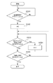
図3に転送要求が発行されてから他のバスマスタが選択された回数をカウントするカウンタの動作を示す。カウンタはバスマスタからのメモリアクセス(転送要求)がアサートされるまでウェイトし(S301)、転送要求のアサートに応じてカウント値iをクリアする、そして、他のバスマスタからの転送要求が受け付けられる毎にカウントし(S303、S304)、当初の転送要求が受け付けられると、カウントを終了する(S305)。このカウンタをバスマスタごとに設ける。 FIG. 3 shows the operation of the counter that counts the number of times another bus master has been selected since the transfer request was issued. The counter waits until a memory access (transfer request) from the bus master is asserted (S301), clears the count value i in response to the assertion of the transfer request, and every time a transfer request from another bus master is accepted. Counting is performed (S303, S304), and when the initial transfer request is accepted, the counting is terminated (S305). This counter is provided for each bus master.
図4は図1に示す調停回路106が、図3で示したカウンタの値を用いて、図2のフローチャートにバスマスタからのアクセス要求のどれを選択するかを決定する処理(S403)を追加したフローチャートである。図4のフローにより所定回数以上許可されなかった省電力モードのメモリに対するアクセス要求は、省電力モードではないメモリに対するアクセスと同様に扱う。
4 adds processing (S403) for determining which access request from the bus master is selected by the
(第3の実施形態)
第2の実施形態では許可されなかった回数を考慮したが、本実施形態では省電力モードのメモリに対するアクセスが優先されない時間の上限を用いる。例えば、調停回路106はバスマスタごとのカウンタを持ち、転送要求が開始されてからの時間をカウントする。カウント値が一定時間に達すると、省電力モードであるバスマスタへのアクセス要求であっても、前記リストに追加する。
(Third embodiment)
In the second embodiment, the number of times of disapproval is considered, but in this embodiment, an upper limit of time during which access to the memory in the power saving mode is not prioritized is used. For example, the
転送要求が発行されてからの時間をカウントするカウンタの動作を示すフローチャートは図3と同様である。この転送要求が発行されてからの時間をカウントするカウンタをバスマスタごとに設ける。図4は図1に示す調停回路106が、図3で示したカウンタの値を用いて、バスマスタからのアクセス要求のどれを選択するかを決定する処理を示すフローチャートである。図4のフローにより転送要求発行後、所定時間以上経過した省電力モードのメモリに対するアクセス要求は、省電力モードではないメモリに対するアクセスと同様に扱われる。
The flowchart showing the operation of the counter that counts the time since the transfer request is issued is the same as that in FIG. A counter that counts the time from when this transfer request is issued is provided for each bus master. FIG. 4 is a flowchart showing a process in which the
以上、上述の実施形態によって省電力モードではないメモリに対するメモリアクセスを優先的にアクセス保持回路103に保持される。
As described above, according to the above-described embodiment, memory access to the memory that is not in the power saving mode is preferentially held in the
なお、上述の実施形態の説明では調停回路106が選択するバスマスタの候補をリストとして調停回路106が保持していたが、リスト形式で保持しなくても、単にバスマスタのID(識別情報)を保持するだけでもよい。なお、上述した複数の実施形態の方法を併用して用いることで、更に細かく複数のメモリアクセスを優先度順に並べることができる。
In the description of the above-described embodiment, the
100 メモリ制御回路
101 省電力モード制御回路
102 省電力モード監視回路
103 アクセス保持回路
104 メモリコマンド生成回路
105 デコード回路
106 調停回路
106 選択回路
110 メモリ0
111 メモリ1
DESCRIPTION OF
111
Claims (7)
前記複数のマスタからのメモリアクセス要求を調停し、前記複数のマスタの1つにメモリアクセス要求を許可する調停手段と、
前記複数のメモリのそれぞれが省電力状態にあるか否かを監視する監視手段とを有し、
前記調停手段は、前記監視手段の検出結果に応じて、省電力状態にあるメモリに対するメモリアクセス要求と省電力状態にないメモリに対するメモリアクセス要求が競合する場合、省電力状態にないメモリに対するメモリアクセス要求を優先的に選択している間に、省電力状態にあるメモリに対するメモリアクセス要求が所定回数以上、受け付けられなかった場合に、省電力状態にあるメモリへのメモリアクセス要求を選択対象に含めることを特徴とするメモリ制御装置。 A memory control device connected between a plurality of masters and a plurality of memories capable of transitioning to a power saving state,
Arbitrating means for arbitrating memory access requests from the plurality of masters, and allowing a memory access request to one of the plurality of masters;
Monitoring means for monitoring whether each of the plurality of memories is in a power saving state,
The arbitration unit, when a memory access request for a memory in a power saving state and a memory access request for a memory not in a power saving state compete with each other according to a detection result of the monitoring unit, If a memory access request for a memory in the power saving state is not accepted more than a predetermined number of times while the request is preferentially selected , the memory access request to the memory in the power saving state is included in the selection target. A memory control device.
前記複数のマスタからのメモリアクセスを調停し、前記複数のマスタの1つにメモリアクセス要求を許可する調停工程と、
前記複数のメモリのそれぞれが省電力状態にあるか否かを監視する監視工程とを有し、
前記調停工程では、前記監視工程の検出結果に応じて、省電力状態にあるメモリに対するメモリアクセス要求と省電力状態にないメモリに対するメモリアクセス要求が競合する場合、省電力状態にないメモリに対するメモリアクセス要求を優先的に選択している間に、省電力状態にあるメモリに対するメモリアクセス要求が所定回数以上、受け付けられなかった場合に、省電力状態にあるメモリへのメモリアクセス要求を選択対象に含めることを特徴とするメモリ制御方法。 A memory control method in a memory control device connected between a plurality of masters and a plurality of memories capable of transitioning to a power saving state,
Arbitrating memory access from the plurality of masters and allowing a memory access request to one of the plurality of masters; and
A monitoring step of monitoring whether each of the plurality of memories is in a power saving state,
In the arbitration step, when a memory access request for a memory in a power saving state and a memory access request for a memory not in a power saving state compete with each other according to a detection result of the monitoring step, a memory access to a memory that is not in a power saving state If a memory access request for a memory in the power saving state is not accepted more than a predetermined number of times while the request is preferentially selected , the memory access request to the memory in the power saving state is included in the selection target. A memory control method.
Priority Applications (1)
| Application Number | Priority Date | Filing Date | Title |
|---|---|---|---|
| JP2011161055A JP5932261B2 (en) | 2010-09-17 | 2011-07-22 | Memory control device and memory control method |
Applications Claiming Priority (3)
| Application Number | Priority Date | Filing Date | Title |
|---|---|---|---|
| JP2010209418 | 2010-09-17 | ||
| JP2010209418 | 2010-09-17 | ||
| JP2011161055A JP5932261B2 (en) | 2010-09-17 | 2011-07-22 | Memory control device and memory control method |
Publications (3)
| Publication Number | Publication Date |
|---|---|
| JP2012084123A JP2012084123A (en) | 2012-04-26 |
| JP2012084123A5 JP2012084123A5 (en) | 2014-09-04 |
| JP5932261B2 true JP5932261B2 (en) | 2016-06-08 |
Family
ID=45818779
Family Applications (1)
| Application Number | Title | Priority Date | Filing Date |
|---|---|---|---|
| JP2011161055A Expired - Fee Related JP5932261B2 (en) | 2010-09-17 | 2011-07-22 | Memory control device and memory control method |
Country Status (2)
| Country | Link |
|---|---|
| US (1) | US8856465B2 (en) |
| JP (1) | JP5932261B2 (en) |
Families Citing this family (3)
| Publication number | Priority date | Publication date | Assignee | Title |
|---|---|---|---|---|
| JP7159002B2 (en) * | 2018-10-26 | 2022-10-24 | キヤノン株式会社 | An information processing apparatus including a device that is in an operation stop state according to an operation stop signal and that can shift to a power saving mode on condition that at least an operation stop signal is not input. |
| US10698846B2 (en) * | 2018-11-07 | 2020-06-30 | Realtek Semiconductor Corporation | DDR SDRAM physical layer interface circuit and DDR SDRAM control device |
| JP7292044B2 (en) * | 2019-02-07 | 2023-06-16 | キヤノン株式会社 | Control device and control method |
Family Cites Families (6)
| Publication number | Priority date | Publication date | Assignee | Title |
|---|---|---|---|---|
| US5664089A (en) * | 1994-04-26 | 1997-09-02 | Unisys Corporation | Multiple power domain power loss detection and interface disable |
| JP2647035B2 (en) | 1994-11-30 | 1997-08-27 | 日本電気株式会社 | Bus control circuit |
| CN100428191C (en) * | 2004-06-24 | 2008-10-22 | 松下电器产业株式会社 | Administration device for warranting local concentrated access in low-band width, administration method, and animation processing apparatus including the administration device |
| US7581073B2 (en) * | 2006-08-09 | 2009-08-25 | International Business Machines Corporation | Systems and methods for providing distributed autonomous power management in a memory system |
| JP5104123B2 (en) * | 2007-08-17 | 2012-12-19 | 富士通セミコンダクター株式会社 | Semiconductor memory |
| US9842068B2 (en) * | 2010-04-14 | 2017-12-12 | Qualcomm Incorporated | Methods of bus arbitration for low power memory access |
-
2011
- 2011-07-22 JP JP2011161055A patent/JP5932261B2/en not_active Expired - Fee Related
- 2011-09-02 US US13/225,294 patent/US8856465B2/en not_active Expired - Fee Related
Also Published As
| Publication number | Publication date |
|---|---|
| JP2012084123A (en) | 2012-04-26 |
| US20120072681A1 (en) | 2012-03-22 |
| US8856465B2 (en) | 2014-10-07 |
Similar Documents
| Publication | Publication Date | Title |
|---|---|---|
| US9372526B2 (en) | Managing a power state of a processor | |
| JP5553392B2 (en) | Thread throttling | |
| US7155618B2 (en) | Low power system and method for a data processing system | |
| US9201777B2 (en) | Quality of service support using stacked memory device with logic die | |
| US8200882B2 (en) | Memory system, access control method therefor, and computer program | |
| JP5893632B2 (en) | Memory controller, system, and method for applying page management policy based on stream transaction information | |
| KR20190022428A (en) | Command arbitration for high-speed memory interfaces | |
| US20160246711A9 (en) | Interface methods and apparatus for memory devices | |
| JP5414350B2 (en) | Memory control circuit and control method thereof | |
| JP2008276391A (en) | Memory access control device | |
| JP2019522257A (en) | Low power memory throttling | |
| JP2014228915A (en) | Data processing device | |
| US8484418B2 (en) | Methods and apparatuses for idle-prioritized memory ranks | |
| US8166316B2 (en) | Single interface access to multiple bandwidth and power memory zones | |
| JP2008009817A (en) | Semiconductor device and data transfer method | |
| JP5932261B2 (en) | Memory control device and memory control method | |
| JP5911548B1 (en) | Apparatus, method, and computer program for scheduling access request to shared memory | |
| JP2009251713A (en) | Cache memory control unit | |
| JP5393289B2 (en) | Memory control circuit, memory system, and control method | |
| US20230090567A1 (en) | Device and method for two-stage transitioning between reduced power states | |
| JP4437386B2 (en) | Signal processing system | |
| JP2010287057A (en) | Memory control circuit |
Legal Events
| Date | Code | Title | Description |
|---|---|---|---|
| A521 | Request for written amendment filed |
Free format text: JAPANESE INTERMEDIATE CODE: A523 Effective date: 20140718 |
|
| A621 | Written request for application examination |
Free format text: JAPANESE INTERMEDIATE CODE: A621 Effective date: 20140718 |
|
| A977 | Report on retrieval |
Free format text: JAPANESE INTERMEDIATE CODE: A971007 Effective date: 20150309 |
|
| A131 | Notification of reasons for refusal |
Free format text: JAPANESE INTERMEDIATE CODE: A131 Effective date: 20150414 |
|
| A521 | Request for written amendment filed |
Free format text: JAPANESE INTERMEDIATE CODE: A523 Effective date: 20150608 |
|
| A131 | Notification of reasons for refusal |
Free format text: JAPANESE INTERMEDIATE CODE: A131 Effective date: 20151117 |
|
| A521 | Request for written amendment filed |
Free format text: JAPANESE INTERMEDIATE CODE: A523 Effective date: 20160116 |
|
| TRDD | Decision of grant or rejection written | ||
| A01 | Written decision to grant a patent or to grant a registration (utility model) |
Free format text: JAPANESE INTERMEDIATE CODE: A01 Effective date: 20160405 |
|
| A61 | First payment of annual fees (during grant procedure) |
Free format text: JAPANESE INTERMEDIATE CODE: A61 Effective date: 20160428 |
|
| R151 | Written notification of patent or utility model registration |
Ref document number: 5932261 Country of ref document: JP Free format text: JAPANESE INTERMEDIATE CODE: R151 |
|
| LAPS | Cancellation because of no payment of annual fees |