JP5931006B2 - Light emitting device - Google Patents
Light emitting device Download PDFInfo
- Publication number
- JP5931006B2 JP5931006B2 JP2013116842A JP2013116842A JP5931006B2 JP 5931006 B2 JP5931006 B2 JP 5931006B2 JP 2013116842 A JP2013116842 A JP 2013116842A JP 2013116842 A JP2013116842 A JP 2013116842A JP 5931006 B2 JP5931006 B2 JP 5931006B2
- Authority
- JP
- Japan
- Prior art keywords
- light
- light emitting
- emitting device
- covering member
- emitting element
- Prior art date
- Legal status (The legal status is an assumption and is not a legal conclusion. Google has not performed a legal analysis and makes no representation as to the accuracy of the status listed.)
- Active
Links
Images


Classifications
-
- H—ELECTRICITY
- H01—ELECTRIC ELEMENTS
- H01L—SEMICONDUCTOR DEVICES NOT COVERED BY CLASS H10
- H01L2224/00—Indexing scheme for arrangements for connecting or disconnecting semiconductor or solid-state bodies and methods related thereto as covered by H01L24/00
- H01L2224/01—Means for bonding being attached to, or being formed on, the surface to be connected, e.g. chip-to-package, die-attach, "first-level" interconnects; Manufacturing methods related thereto
- H01L2224/10—Bump connectors; Manufacturing methods related thereto
- H01L2224/15—Structure, shape, material or disposition of the bump connectors after the connecting process
- H01L2224/16—Structure, shape, material or disposition of the bump connectors after the connecting process of an individual bump connector
- H01L2224/161—Disposition
- H01L2224/16151—Disposition the bump connector connecting between a semiconductor or solid-state body and an item not being a semiconductor or solid-state body, e.g. chip-to-substrate, chip-to-passive
- H01L2224/16221—Disposition the bump connector connecting between a semiconductor or solid-state body and an item not being a semiconductor or solid-state body, e.g. chip-to-substrate, chip-to-passive the body and the item being stacked
- H01L2224/16225—Disposition the bump connector connecting between a semiconductor or solid-state body and an item not being a semiconductor or solid-state body, e.g. chip-to-substrate, chip-to-passive the body and the item being stacked the item being non-metallic, e.g. insulating substrate with or without metallisation
-
- H—ELECTRICITY
- H01—ELECTRIC ELEMENTS
- H01L—SEMICONDUCTOR DEVICES NOT COVERED BY CLASS H10
- H01L2224/00—Indexing scheme for arrangements for connecting or disconnecting semiconductor or solid-state bodies and methods related thereto as covered by H01L24/00
- H01L2224/01—Means for bonding being attached to, or being formed on, the surface to be connected, e.g. chip-to-package, die-attach, "first-level" interconnects; Manufacturing methods related thereto
- H01L2224/26—Layer connectors, e.g. plate connectors, solder or adhesive layers; Manufacturing methods related thereto
- H01L2224/31—Structure, shape, material or disposition of the layer connectors after the connecting process
- H01L2224/32—Structure, shape, material or disposition of the layer connectors after the connecting process of an individual layer connector
- H01L2224/321—Disposition
- H01L2224/32151—Disposition the layer connector connecting between a semiconductor or solid-state body and an item not being a semiconductor or solid-state body, e.g. chip-to-substrate, chip-to-passive
- H01L2224/32221—Disposition the layer connector connecting between a semiconductor or solid-state body and an item not being a semiconductor or solid-state body, e.g. chip-to-substrate, chip-to-passive the body and the item being stacked
- H01L2224/32225—Disposition the layer connector connecting between a semiconductor or solid-state body and an item not being a semiconductor or solid-state body, e.g. chip-to-substrate, chip-to-passive the body and the item being stacked the item being non-metallic, e.g. insulating substrate with or without metallisation
-
- H—ELECTRICITY
- H01—ELECTRIC ELEMENTS
- H01L—SEMICONDUCTOR DEVICES NOT COVERED BY CLASS H10
- H01L2224/00—Indexing scheme for arrangements for connecting or disconnecting semiconductor or solid-state bodies and methods related thereto as covered by H01L24/00
- H01L2224/01—Means for bonding being attached to, or being formed on, the surface to be connected, e.g. chip-to-package, die-attach, "first-level" interconnects; Manufacturing methods related thereto
- H01L2224/42—Wire connectors; Manufacturing methods related thereto
- H01L2224/47—Structure, shape, material or disposition of the wire connectors after the connecting process
- H01L2224/48—Structure, shape, material or disposition of the wire connectors after the connecting process of an individual wire connector
- H01L2224/4805—Shape
- H01L2224/4809—Loop shape
- H01L2224/48091—Arched
-
- H—ELECTRICITY
- H01—ELECTRIC ELEMENTS
- H01L—SEMICONDUCTOR DEVICES NOT COVERED BY CLASS H10
- H01L2224/00—Indexing scheme for arrangements for connecting or disconnecting semiconductor or solid-state bodies and methods related thereto as covered by H01L24/00
- H01L2224/01—Means for bonding being attached to, or being formed on, the surface to be connected, e.g. chip-to-package, die-attach, "first-level" interconnects; Manufacturing methods related thereto
- H01L2224/42—Wire connectors; Manufacturing methods related thereto
- H01L2224/47—Structure, shape, material or disposition of the wire connectors after the connecting process
- H01L2224/48—Structure, shape, material or disposition of the wire connectors after the connecting process of an individual wire connector
- H01L2224/481—Disposition
- H01L2224/48151—Connecting between a semiconductor or solid-state body and an item not being a semiconductor or solid-state body, e.g. chip-to-substrate, chip-to-passive
- H01L2224/48221—Connecting between a semiconductor or solid-state body and an item not being a semiconductor or solid-state body, e.g. chip-to-substrate, chip-to-passive the body and the item being stacked
- H01L2224/48225—Connecting between a semiconductor or solid-state body and an item not being a semiconductor or solid-state body, e.g. chip-to-substrate, chip-to-passive the body and the item being stacked the item being non-metallic, e.g. insulating substrate with or without metallisation
- H01L2224/48227—Connecting between a semiconductor or solid-state body and an item not being a semiconductor or solid-state body, e.g. chip-to-substrate, chip-to-passive the body and the item being stacked the item being non-metallic, e.g. insulating substrate with or without metallisation connecting the wire to a bond pad of the item
-
- H—ELECTRICITY
- H01—ELECTRIC ELEMENTS
- H01L—SEMICONDUCTOR DEVICES NOT COVERED BY CLASS H10
- H01L2224/00—Indexing scheme for arrangements for connecting or disconnecting semiconductor or solid-state bodies and methods related thereto as covered by H01L24/00
- H01L2224/73—Means for bonding being of different types provided for in two or more of groups H01L2224/10, H01L2224/18, H01L2224/26, H01L2224/34, H01L2224/42, H01L2224/50, H01L2224/63, H01L2224/71
- H01L2224/732—Location after the connecting process
- H01L2224/73201—Location after the connecting process on the same surface
- H01L2224/73203—Bump and layer connectors
- H01L2224/73204—Bump and layer connectors the bump connector being embedded into the layer connector
-
- H—ELECTRICITY
- H01—ELECTRIC ELEMENTS
- H01L—SEMICONDUCTOR DEVICES NOT COVERED BY CLASS H10
- H01L2224/00—Indexing scheme for arrangements for connecting or disconnecting semiconductor or solid-state bodies and methods related thereto as covered by H01L24/00
- H01L2224/73—Means for bonding being of different types provided for in two or more of groups H01L2224/10, H01L2224/18, H01L2224/26, H01L2224/34, H01L2224/42, H01L2224/50, H01L2224/63, H01L2224/71
- H01L2224/732—Location after the connecting process
- H01L2224/73251—Location after the connecting process on different surfaces
- H01L2224/73265—Layer and wire connectors
-
- H—ELECTRICITY
- H01—ELECTRIC ELEMENTS
- H01L—SEMICONDUCTOR DEVICES NOT COVERED BY CLASS H10
- H01L2924/00—Indexing scheme for arrangements or methods for connecting or disconnecting semiconductor or solid-state bodies as covered by H01L24/00
- H01L2924/15—Details of package parts other than the semiconductor or other solid state devices to be connected
- H01L2924/181—Encapsulation
Description
本発明は、発光装置に関し、特に発光素子からの光の取り出し効率を増大させるための
光透過部材および被覆部材を備える発光装置に関する。
The present invention relates to a light emitting device, and more particularly to a light emitting device including a light transmitting member and a covering member for increasing light extraction efficiency from a light emitting element.
近年、光源として発光ダイオード(Light Emitting Diode:LED)やレーザダイオー
ド(Laser Diode:LD)等の半導体発光素子を搭載した発光装置は、各種の照明や表示
装置に利用されている。特に、これら半導体発光素子は消費電力が低く長寿命であるため
、蛍光灯に代替可能な次世代照明の光源として注目を集めており、さらなる発光出力およ
び発光効率の向上が求められている。
2. Description of the Related Art In recent years, light-emitting devices equipped with semiconductor light-emitting elements such as light-emitting diodes (LEDs) and laser diodes (LDs) as light sources have been used for various lighting and display devices. In particular, since these semiconductor light emitting devices have low power consumption and long life, they are attracting attention as light sources for next-generation illumination that can be replaced with fluorescent lamps, and further improvements in light emission output and light emission efficiency are required.
例えば、特許文献1で提案されている発光装置は、LEDである発光素子チップが、実
装基板であるパッケージに設けられた収納凹所の底部にフリップチップ実装されている。
また、発光素子チップの出射面には、平凸レンズの形状を有した光取出増大部材の入射面
が光結合されている。光取出増大部材は、発光素子チップのサファイア基板と空気との中
間の屈折率を有している。そして、光取出増大部材の出射面は球面であって、出射面上の
すべての位置において、当該位置の法線を中心線とし臨界角を中心線と母線とのなす角度
とする円錐内に発光素子チップの出射面が含まれるように形成されている。この構成によ
れば、光取出増大部材の出射面において実質的に全反射を生じないから、多重反射による
光の減衰や消滅を生じさせずに光取出増大部材から光を取り出すことができ、結果的に光
の利用効率が高くできるとされている。
For example, in the light-emitting device proposed in
In addition, an incident surface of the light extraction increasing member having the shape of a plano-convex lens is optically coupled to the emission surface of the light emitting element chip. The light extraction increasing member has an intermediate refractive index between the sapphire substrate of the light emitting element chip and air. The exit surface of the light extraction increasing member is a spherical surface, and at all positions on the exit surface, light is emitted within a cone whose normal is the center line and whose critical angle is the angle between the center line and the generatrix. The output surface of the element chip is included. According to this configuration, substantially no total reflection occurs on the exit surface of the light extraction increasing member, so that light can be extracted from the light extraction increasing member without causing attenuation or extinction of light due to multiple reflection. Therefore, it is said that the light use efficiency can be increased.
しかしながら、上記特許文献1に記載された発光装置において、発光素子チップからそ
の側方へ出射される光は、封止樹脂を透過して、その内部を伝搬することでこの封止樹脂
やパッケージにより吸収・減衰される。また、封止樹脂からも光取出増大部材の入射面に
光結合するため、入射面における発光領域は実質的に大きくなり、光取出増大部材の出射
面において反射される光成分が増加する。これらのことから、発光素子チップから出射さ
れる光を十分に外部に取り出すことができず、また光の取り出し効率を維持したまま装置
の更なる小型化を図ることが難しい。
However, in the light-emitting device described in
また、従来は光源としてLED光を想定し、その取り出し効率を高める構造であり、取
り出されたLED光を、別途設けた蛍光体などにより波長変換させる構造となっている。
そのため、発光装置の出射光としての波長変換光、それに付加されたLED光、について
、分離されたLED光源部と波長変換部との間での光散乱、吸収などにより、その光取り
出し効率が低下する構造となっていたり、その出射光の指向性が低下する構造となってい
たり、色むら、輝度むらが大きくなる構造となっていたり、装置の出射光の発光特性が不
十分なものとなっている場合がある。さらにこのような光源と変換部の分離構造では、装
置全体の小型化が難しい側面もある。
Conventionally, LED light is assumed as a light source, and the extraction efficiency is increased. The extracted LED light is wavelength-converted by a separately provided phosphor or the like.
Therefore, the light extraction efficiency of the wavelength converted light as the emitted light of the light emitting device and the LED light added thereto are reduced due to light scattering and absorption between the separated LED light source unit and the wavelength converting unit. The structure of the device is such that the directivity of the emitted light is reduced, the color unevenness and the luminance unevenness are increased, or the emission characteristics of the emitted light of the device are insufficient. There may be. Furthermore, in such a separation structure of the light source and the conversion unit, there is a side where it is difficult to reduce the size of the entire apparatus.
本発明は、上記課題に鑑みてなされたものであり、その目的は、発光素子から出射され
る光の取り出し効率を向上させること、小型化できること、発光効率を高くすること、色
むら、輝度むらを抑えた発光特性とすること、が可能な発光装置を提供することである。
The present invention has been made in view of the above problems, and its purpose is to improve the extraction efficiency of light emitted from the light emitting element, to be able to reduce the size, to increase the light emission efficiency, color unevenness, and luminance unevenness. It is an object of the present invention to provide a light-emitting device capable of achieving light emission characteristics with suppressed light emission.
本発明に係る発光装置は、下記(1)〜(13)の構成により、上記目的を達成するこ
とができる。
(1) 光反射性材料を含有する被覆部材と、発光側の表面と、前記被覆部材の表面に対
向し、該表面内に配置された光入射側の表面とを有する光透過部材と、前記光透過部材の
光入射側表面において、外側の反射領域に囲まれた入射領域に結合し、前記被覆部材に一
部が埋め込まれた光源部に、発光素子と、該発光素子の前記入射領域側に結合され、該発
光素子に励起される波長変換部材と、を備える発光装置。
(2) 前記光透過部材は、前記発光側が凸曲面で、前記光入射側の少なくとも反射領域
が略平坦な表面であり、前記入射領域の断面幅は、前記光入射側表面の半分以下である上
記(1)に記載の発光装置。
(3) 光反射性材料を含有する被覆部材と、凸曲面の発光側の表面と、前記被覆部材の
表面に対向し、該表面内に配置された光入射側の表面とを有する光透過部材と、前記光透
過部材の光入射側表面において、略平坦な表面の反射領域に囲まれた内側の入射領域に結
合し、前記被覆部材に一部が埋め込まれた光源部が設けられて、該光源部内に設けられた
発光素子と、を備え、前記入射領域の断面幅は、前記光入射側表面の半分以下である発光
装置。
(4) 前記発光装置は、前記光源部に、前記発光素子の前記入射領域側に結合され、前
記発光素子に励起される波長変換部材をさらに備える上記(3)に記載の発光装置。
(5) 前記波長変換部材は、互いに対向する第1及び第2の主面を有する板状体であっ
て、前記第2の主面に複数の前記発光素子が接合されており、前記入射領域に前記第1の
主面が接合されている上記(1),(2),(4)のいずれか1つに記載の発光装置。
(6) 前記反射領域は、前記被覆部材の表面と離間された前記光透過部材表面に設けら
れる上記(1)乃至(5)のいずれか1つに記載の発光装置。
(7) 前記発光装置は、前記光透過部材の光入射側の表面と前記被覆部材の表面とを接
着させる透光性接着材を有し、前記入射領域及び反射領域は、前記透光性接着剤との界面
に設けられる上記(1)乃至(6)のいずれか1つに記載の発光装置。
(8) 前記光透過部材は、前記光源部上及び前記被覆部材表面に設けられ、前記反射領
域は、前記光透過部材と前記被覆部材との界面である上記(1)乃至(5)のいずれか1
つに記載の発光装置。
(9) 前記入射領域は、前記反射領域より前記発光側に突出している上記(8)に記載
の発光装置。
(10) 前記光透過部材の発光側の表面形状は、球面形状である上記(1)乃至(9)
のいずれか1つに記載の発光装置。
(11) 前記発光装置は、前記発光素子が実装される実装基板を有し、前記発光素子は
、前記入射領域側の表面に対向する実装面側で、前記実装基板と電気的に接続される上記
(1)乃至(10)のいずれか1つに記載の発光装置。
(12) 前記発光装置の光源部は、前記発光素子の入射領域側表面に結合して、発光素
子により励起される波長変換部材を有し、前記被覆部材は、前記入射領域から、前記光源
部の側面を覆って、前記実装基板の表面上にまで延在して設けられている上記(11)に
記載の発光装置。
(13) 前記被覆部材が、前記発光素子及び前記波長変換部材の側面にそれぞれ接して
設けられる上記(12)に記載の発光装置。
The light emitting device according to the present invention can achieve the above object by the following configurations (1) to (13).
(1) A light-transmitting member having a light-reflecting material-containing covering member, a light-emitting surface, and a light-incident-side surface disposed in the surface, facing the surface of the covering member; On the light incident side surface of the light transmitting member, a light source element coupled to an incident region surrounded by an outer reflective region and partially embedded in the covering member, a light emitting element, and the incident region side of the light emitting element And a wavelength conversion member that is coupled to and excited by the light emitting element.
(2) The light transmitting member has a convex curved surface on the light emitting side and a surface in which at least the reflective region on the light incident side is substantially flat, and a cross-sectional width of the incident region is not more than half of the surface on the light incident side. The light emitting device according to (1) above.
(3) A light-transmitting member having a light-reflecting material-containing covering member, a light-emitting surface having a convex curved surface, and a light-incident-side surface disposed in the surface facing the surface of the covering member And a light source side surface of the light transmissive member coupled to an inner incident region surrounded by a reflection region of a substantially flat surface, and a light source part partially embedded in the covering member is provided, A light emitting device provided in a light source unit, wherein a cross-sectional width of the incident region is not more than half of the light incident side surface.
(4) The light emitting device according to (3), further including a wavelength conversion member coupled to the light source unit on the incident region side of the light emitting element and excited by the light emitting element.
(5) The wavelength conversion member is a plate-like body having first and second main surfaces facing each other, and a plurality of the light emitting elements are bonded to the second main surface, and the incident region The light-emitting device according to any one of (1), (2), and (4), wherein the first main surface is bonded to the light-emitting device.
(6) The light-emitting device according to any one of (1) to (5), wherein the reflection region is provided on a surface of the light transmission member that is separated from a surface of the covering member.
(7) The light-emitting device includes a light-transmitting adhesive that adheres the light-incident-side surface of the light-transmitting member and the surface of the covering member, and the incident region and the reflective region are the light-transmitting adhesive. The light emitting device according to any one of (1) to (6), which is provided at an interface with the agent.
(8) Any of the above (1) to (5), wherein the light transmitting member is provided on the light source unit and on the surface of the covering member, and the reflection region is an interface between the light transmitting member and the covering member. Or one
The light-emitting device as described in one.
(9) The light emitting device according to (8), wherein the incident region protrudes toward the light emitting side from the reflective region.
(10) The surface shape on the light emitting side of the light transmitting member is a spherical shape described in (1) to (9) above.
The light emitting device according to any one of the above.
(11) The light emitting device includes a mounting board on which the light emitting element is mounted, and the light emitting element is electrically connected to the mounting board on a mounting surface side facing the surface on the incident region side. The light emitting device according to any one of (1) to (10) above.
(12) The light source unit of the light emitting device includes a wavelength conversion member that is coupled to the incident region side surface of the light emitting element and is excited by the light emitting element, and the covering member extends from the incident region to the light source unit. The light-emitting device according to (11), wherein the light-emitting device is provided so as to cover a side surface of the mounting substrate and extend to the surface of the mounting substrate.
(13) The light emitting device according to (12), wherein the covering member is provided in contact with side surfaces of the light emitting element and the wavelength conversion member.
本発明は、光反射性の被覆部材により、光源部の発光素子、それに結合する波長変換部
を被覆して、発光素子の光源、又はその複合的な光源からの出射光を一方向に取り出し、
すなわち、光源を1つの発光面として、発光装置の光出射の窓部を一面の特定の領域とし
、上記窓部を内包する光透過部材を接合させて被覆部材に覆われることにより、光源から
の光の取り出し効率を格段に向上させ、色と輝度むらを抑えた発光特性を得ることができ
る。特に、光透過部材の一部領域において窓部に結合させ、他の領域において光透過部材
の内面で反射される光成分が、被覆部材で反射されることで、光を効率良く取り出すこと
ができ、すなわち、部材中を伝搬する光成分が多い光透過部材であっても取り出し効率を
高くできるため、比較的大きな面積、容積を占める光透過部材を小さくして、装置を小型
化した場合にも特性の低下を抑えることができる。また、上記複合的な光源としているた
め、その光源部を小さくでき、これも装置の小型化に寄与する。
The present invention covers the light emitting element of the light source unit and the wavelength conversion unit coupled thereto with the light-reflective coating member, and extracts the light emitted from the light source of the light emitting element or the composite light source in one direction,
That is, the light source is one light emitting surface, the light emitting window of the light emitting device is a specific area on one surface, and the light transmitting member that includes the window is joined and covered with the covering member, thereby The light extraction efficiency can be significantly improved, and light emission characteristics with suppressed color and luminance unevenness can be obtained. In particular, it is possible to efficiently extract light by being coupled to the window portion in a part of the light transmitting member and reflecting the light component reflected from the inner surface of the light transmitting member in the other region by the covering member. That is, even if the light transmitting member has a large amount of light component propagating in the member, the extraction efficiency can be increased. Therefore, even if the light transmitting member occupying a relatively large area and volume is reduced and the device is downsized. The deterioration of characteristics can be suppressed. Moreover, since it is set as the said composite light source, the light source part can be made small and this also contributes to size reduction of an apparatus.
以下、発明の実施の形態について適宜図面を参照して説明する。ただし、以下に説明す
る発光素子・装置は、本発明の技術思想を具体化するためのものであって、本発明を以下
のものに特定しない。特に、以下に記載されている構成部品の寸法、材質、形状、その相
対的配置等は特定的な記載がない限りは、本発明の範囲をそれのみに限定する趣旨ではな
く、単なる説明例にすぎない。なお、各図面が示す部材の大きさや位置関係等は、説明を
明確にするため誇張していることがある。さらに、本発明を構成する各要素は、複数の要
素を同一の部材で構成して一の部材で複数の要素を兼用する態様としてもよいし、逆に一
の部材の機能を複数の部材で分担して実現することもできる。また、以下に記載されてい
る各実施の形態についても同様に、特に排除する記載が無い限りは各構成等を適宜組み合
わせて適用できる。
Hereinafter, embodiments of the invention will be described with reference to the drawings as appropriate. However, the light-emitting element / device described below is for embodying the technical idea of the present invention, and the present invention is not limited to the following. In particular, the dimensions, materials, shapes, relative arrangements, and the like of the components described below are not intended to limit the scope of the present invention only to specific examples unless otherwise specified. Only. Note that the size, positional relationship, and the like of the members shown in each drawing may be exaggerated for clarity of explanation. Furthermore, each element constituting the present invention may be configured such that a plurality of elements are constituted by the same member and the plurality of elements are shared by one member, and conversely, the function of one member is constituted by a plurality of members. It can also be realized by sharing. Similarly, each embodiment described below can be applied by appropriately combining the components and the like unless otherwise specified.
(実施の形態1)
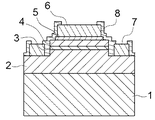
図1、2は、本発明の実施の形態1に係る発光装置100の概略図であり、図1(a)
は概略上面図の図1(b)のA−Aにおける概略断面図であり、図2は光源部周辺の概略
断面図である。図1,2に示す例の発光装置100は、主として、発光素子10と、光透
過部材20と、被覆部材30と、波長変換部材40と、実装基板50と、から構成される
。基板50は、枠体55と、複数個(図中では2個)の発光素子10がフリップチップ実
装された配線51を備えている。この波長変換部材40は、板状で互いに対向する第1お
よび第2の面を有し、その第2の面が各発光素子10の裏面に接合されている。そして、
光反射材料35を含有する被覆部材30が枠体55の内側に充填され、光源部の発光素子
10と波長変換部材40は、第1の面を露出面として、被覆部材30に被覆されている。
被覆部材30は、側面と第2の面の一部、さらに発光素子10の側面と、を連続して被覆
する。これにより、発光素子10及び/又は波長変換部材40から出射された光は、光反
射性の被覆部材30により発光側に反射、導光されて、波長変換部材40の第1の面から
取り出され、この第1の面を主要な光取り出しの窓部すなわち発光面とする面発光型の光
源となる。第1の面の形状、大きさでそれを光源とでき、この光源の上に、光源に対する
光学素子として光透過部材20がその光入射側の一部領域の光入射領域80に接合されて
いる。
(Embodiment 1)
1 and 2 are schematic views of the light-emitting
FIG. 2 is a schematic cross-sectional view taken along line AA of FIG. 1B in a schematic top view, and FIG. 2 is a schematic cross-sectional view around the light source unit. The
The covering
The covering
図2は、実施の形態1に係る発光装置の光源部周辺を説明するための概略断面図である
。図2に示すように、光透過部材20は、その光入射側の表面において、波長変換部材4
0の第1の面を内包し、その外側を囲む被覆部材30の一部に設けられており、その光入
射側の表面に対向して、発光装置の発光面となる発光側の表面21を有する。この光入射
側の表面は、波長変換部材40の第1の面と対向し、発光素子10及び/又は波長変換部
材40からの光が入射される入射領域80と、その外側の被覆部材30表面に対向する反
射領域90と、を有する。この入射領域80は、波長変換部材40の第1の面からの光の
取り出し効率を増大させ、また、図1及び図2に示すように、反射領域90で光透過部材
20の光を反射する。ここで、図示するように、光透過部材20は半球状レンズで、その
中心は図3Aに示すように光源部表面で入射領域の略中心となっており、すなわち凸曲面
の発光面21を備えた光学素子となっている。このとき、波長変換部材40の第1の面に
垂直な断面において、光源部、入射領域80の径(断面幅)Lは、光透過部材20の曲率
半径r(=R/2)の半分以下、L≦(R/2)/2、となっていることが好ましい。入
射領域80から入射した光の一部は発光側の表面21から外部に放出され、残りの光成分
は発光側の表面21の内面で光入射側へ反射されて戻り光となる。この戻り光は、直接、
又は光透過部材20の内面での多重反射を繰り返しながらその多くが、反射領域90に到
達する。反射領域90に入射された戻り光は、光反射性の被覆部材30の表面で反射され
ることにより、光透過部材20の発光側の表面21への入射角が変えられ外部への透過が
促進される。ここで、後述するように、被覆部材が光反射性材料を備えた透光性の部材で
あると、その表面における乱反射効果が高められ、また光の損失が少なく、好ましい。
FIG. 2 is a schematic cross-sectional view for explaining the periphery of the light source unit of the light emitting device according to the first embodiment. As shown in FIG. 2, the
The light emitting
Alternatively, many of them reach the
また、上述のように、発光素子10、又は、発光素子10と波長変換部材40からなる
光源部からの光透過部材20への光入射は、光反射性の被覆部材30にその光源部の一部
が埋め込まれることよって入射領域80にほぼ限定されているため、光は反射領域90か
ら光透過部材20へ直接的に殆ど入射されず、この発光領域を光透過部材20に対して点
光源に近づけることができる。これにより、凸曲面を備えた光学素子の光透過部材の発光
側の表面21での光反射を低減して、ひいては高い光取り出し効率を維持したまま装置全
体を小型化、薄型化することが可能となる。このように、本発明の発光装置は、光透過部
材20の光入射側の表面に、光透過部材20内に高効率に光源部を結合させる入射領域8
0と、その光透過部材内の光成分を発光側の表面21方向に反射させる反射領域90と、
を有し、その異なる作用により、光透過部材20の発光側の表面21の多様な形状に対応
して、光の取り出し効率を格段に向上させることができる。
In addition, as described above, light incident on the
0, a
Due to the different actions, the light extraction efficiency can be remarkably improved corresponding to various shapes of the light-emitting
特に、本実施の形態1においては、光透過部材20の光入射側の表面は、光源部、すな
わち波長変換部材40の第1の面と、その外側の被覆部材30の表面と、に各々直接接合
され、すなわち入射領域80は第1の面との界面に、反射領域90は被覆部材30の表面
との界面に、それぞれ設けられている。したがって、この反射領域90に到達する戻り光
を、光反射性の被覆部材30の表面で反射若しくは散乱せしめ、発光側の表面21を透過
させ装置外部に取り出すことができる。特に、後述するように、被覆部材が光反射性材料
を含有する透光性の部材、例えば透光性樹脂である場合には、被覆部材表面で、光透過部
材との界面反射ができ、さらに内部に入射した光は、光反射性材料により反射、散乱され
るため、反射領域90の効果を高められ、発光特性に優れた発光装置となる。このような
実施の形態1の発光装置100は、後述するように上記面発光型の光源部を作製した後、
その上に光透過部材20を各種成形技術により直接接合させて成形することにより作製す
ることができ、後述する他の実施の形態の発光装置に比して、最も量産性に優れる形態で
ある。
In particular, in the first embodiment, the light incident side surface of the
Further, the
また、入射領域80は、図示するように、反射領域90より発光側に突出していること
が好ましい。これにより、被覆部材30の表面により遮光されず、さらに図示するように
、反射領域90を突出した入射領域80に向けて反射領域から傾斜した傾斜面、すなわち
外側に反射する傾斜面とすれば、その反射領域90による光透過部材20側方への光放出
、すなわち発光装置からの高角度成分を増大させ、広い配向性が得られる。
Moreover, it is preferable that the incident area |
(光学素子と光源)
本発明における光透過部材20、すなわち光学素子の径W、凸曲面の曲率半径rと、入
射領域80の径Lとの関係について、以下にこれを詳述する。図3は、ここで検討する理
論計算モデルの各発光装置の構造を示す概略断面図である。図3(A)に示す発光装置1
10は、一辺の長さLの正方形で厚さ100μmの直方体(板状)の光源部16を備える
。また、光源部は、その上面のみを露出して、その側面及び底面を被覆部材31により被
覆し、被覆部材31の反射率は100%とする。そして、図中の黒丸で示す光源部の上面
の中心を曲率中心とする直径Rの半球状の光透過部材20aが、同一面の光源部及び被覆
部材表面上に設けられている。光透過部材の直径R及び径Wは4mm(曲率半径2mm)
とし、屈折率は1.537とする。この発光装置110は、上述の実施の形態1の発光装
置100を想定している。また、図3(B)に示す発光装置120は、光透過部材20b
と被覆部材32の表面との間に空隙86が設けられて、この両表面が互いに離間されてい
るほかは、上述の発光装置110と同様である。より詳細には、光源部16より外側の光
透過部材20bの平坦な表面(反射領域)に対向して、光源部の上面より下方に傾斜した
傾斜面94があり、空隙86の空気の屈折率は1.000とする。この発光装置120は
、後述する実施の形態2の発光装置200を想定している。
(Optical element and light source)
The relationship between the light transmitting
10 is provided with a
And the refractive index is 1.537. The
And the surface of the covering
また、図3(C)に示す発光装置130は、光源部16が被覆部材33表面上に設けら
れているほかは、上記発光装置110と同様であり、光源部は光透過部材20c内に埋め
込まれて、底面を除いて被覆されており、図中の黒丸で示すように曲率中心は光源部16
の底面の中心に位置する。さらに、図3(D)に示す発光装置140は、光透過部材が設
けられる表面が、被覆部材34とその外側に反射率の低い基材35を備えること、並びに
光透過部材20dを変更したこと以外は、発光装置110と同様である。詳細には、被覆
部材34は他の装置同様に100%の反射率とし、上面視において一辺が2.7mmの正
方形であり、基材35は90%の反射率とし、被覆部材34の外側で光透過部材の全領域
を構成している。光透過部材20dは、光源部上面の中心から直下へ2mm離れた位置に
曲率中心を有する曲率半径3mmの球面であり、径Wは約4.472mmである。したが
って、この発光装置140は、光透過部材の光入射側の表面において、入射領域の外側の
被覆部材34による反射率100%の領域と、さらにその外側の基材35に反射率90%
の領域と、を有しており、光源側の表面は半球面の扁形面となっている。
The
Located in the center of the bottom of the. Further, in the
The surface on the light source side is a hemispherical flat surface.
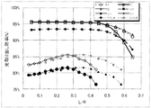
上述の各発光装置110、120、130、140を元に、光透過部材の曲率半径r(
R/2)又は径(断面幅)Wと、入射領域の径(断面幅)Lの比(L/R,L/W)と、
光取り出し効率との関係を、各モデルについて理論計算により解析する。図4はその解析
結果であり、モデルA〜Cは上記装置110〜130、モデルADは上記装置110の被
覆部材31を装置140の被覆部材34及び基材35に置き換えたモデル、モデルDDと
DD−Wは上記装置140とそれをL/W比にしたもの、モデルDAとDA−Wは上記装
置140で被覆部材34と基材35を装置110の被覆部材31に置き換えたモデルとそ
れをL/W比にしたもの、をそれぞれ示し、光源部16の径Lを変化させている。図4に
示すように、モデルA〜CとAD、DD−W、DA−Wの発光装置において、L/R比(
モデルDD−WとDA−Wは、L/W比)が0.5より大きくなると、光の取り出し効率
が低下し始め、特にモデルA〜C、ADではそれが顕著となる。これは、0.5以下の範
囲では、半球面、凸曲面の光透過部材の発光側の表面に対して、光源部が点光源に近い光
取り出し効率にできることを示している。また、モデルA〜Cを比較すると、モデルAと
Bは、比較例のモデルCに比して、L/Rが大きい領域においても光取り出し効率の低下
量が大幅に抑制され、光源部16の一部を光反射性の被覆部材により被覆する構造は、高
い発光効率を維持したまま装置を小型化する上で優位性があることが分かる。また、比較
例のモデルADでは光源が小さい領域でも、モデルA〜Cより効率が低く、またL/Rが
0.5以上で急激に低下するため、モデルA〜Cに比して、光源部を十分に小さく、然る
に光透過部材を十分に大きくしなければならず、高効率化には装置の大型化が必要である
ことを示している。
Based on each of the
R / 2) or diameter (cross-sectional width) W and the ratio (L / R, L / W) of the diameter (cross-sectional width) L of the incident region;
The relationship with the light extraction efficiency is analyzed by theoretical calculation for each model. FIG. 4 shows the analysis results. Models A to C are the
When the models DD-W and DA-W have an L / W ratio (greater than 0.5), the light extraction efficiency begins to decrease, and this is particularly noticeable in the models A to C and AD. This indicates that in the range of 0.5 or less, the light source unit can achieve light extraction efficiency close to that of a point light source with respect to the light emitting side surface of the light-transmitting member having a hemispherical surface and a convex curved surface. Further, when the models A to C are compared with each other, the models A and B are significantly less reduced in light extraction efficiency even in the region where the L / R is larger than the model C of the comparative example. It can be seen that a structure in which a part is covered with a light-reflective coating member has an advantage in downsizing the apparatus while maintaining high luminous efficiency. Further, in the model AD of the comparative example, even in a region where the light source is small, the efficiency is lower than that of the models A to C, and the L / R decreases rapidly when 0.5 or more. However, it is necessary to make the light transmitting member sufficiently large, and it is necessary to increase the size of the apparatus for high efficiency.
さらに、発光装置140の光透過部材20dを用いたモデルDA,DDの光取り出し効
率は、他の発光装置110〜130の光透過部材20a〜cを用いたモデルA〜C,AD
に比して、その初期値、最大値が大幅に低くなっている。光取り出し効率の観点において
、光透過部材の発光側の表面の形状は半球面であることが最も好ましい反面、装置が大型
化する。他方、半球面の扁形の部材20dの発光装置140(モデルDA,DD)では、
光透過部材20d内面での光反射成分が多くなり、効率が低下するが、装置の小型化、薄
型化に優れる。このモデルDA,DDを比較しても、比較例のモデルDD(装置140)
に比して、モデルDAの効率が優れる傾向にあり、本発明が小型化、薄型化においても高
効率の装置を実現できることが分かる。また、発光装置140のように、光透過部材20
の光入射側の表面の外縁に反射率の低い領域35を有するモデルAD、DDは比較例であ
り、このような領域は例えば基板50、配線51などの被覆部材より低い装置内の部材が
露出される構造を想定している。そのため、このモデルでは装置の小型化、光源部の大面
積化により、内面での光反射が増大し、この環状で外縁を構成する低反射率領域に到達す
る光量が増し、さらに光取り出し効率が低下することとなる。本発明の光透過部材が半球
面からの扁形であったり、扁平した、曲率が変わった凸曲面であったり、また図9(b)
、(c)のように種々の光学レンズ形状であったりして、光透過部材の内面反射が多くな
る構造でも、高い発光効率を有し、そして高効率を維持して装置を小型化、薄型化するこ
とができる。
Furthermore, the light extraction efficiency of the models DA and DD using the
The initial and maximum values are significantly lower than From the viewpoint of light extraction efficiency, it is most preferable that the shape of the light transmission side surface of the light transmitting member is a hemispherical surface, but the apparatus is enlarged. On the other hand, in the light emitting device 140 (model DA, DD) of the hemispherical
Although the light reflection component on the inner surface of the
It can be seen that the efficiency of the model DA tends to be superior to that of the model DA, and that the present invention can realize a highly efficient device even in the downsizing and thinning. Further, like the
The models AD and DD having the
(C) Even if it has various optical lens shapes and has a structure in which the internal reflection of the light transmitting member increases, it has high luminous efficiency, and the device is downsized and thin while maintaining high efficiency. Can be
次に、本発明の発光装置の各構成部材および構造について、以下に詳述する。 Next, each component and structure of the light emitting device of the present invention will be described in detail below.
(発光素子)
発光素子10は公知のもの、具体的には半導体発光素子を利用でき、特にGaN系半導
体であれば、蛍光物質を効率良く励起できる短波長の可視光や紫外光が発光可能であるた
め好ましい。具体的な発光ピーク波長は240nm以上560nm以下、好ましくは38
0nm以上470nm以下である。なお、このほか、ZnSe系、InGaAs系、Al
InGaP系半導体の発光素子でもよい。
(Light emitting element)
As the light-emitting
It is 0 nm or more and 470 nm or less. In addition, ZnSe, InGaAs, Al
A light emitting element of an InGaP semiconductor may be used.
(発光素子構造)
半導体層による発光素子構造11は、図5に例示するように少なくとも第1導電型(n
型)層2と第2導電型(p型)層3とにより構成され、更にその間に活性層3を有する構
造が好ましい。また、電極構造は、一方の主面側に第1導電型、第2導電型の両電極6,
7が設けられる同一面側電極構造が好ましいが、半導体層の各主面に対向して電極が各々
設けられる対向電極構造でも良い。発光素子10の実装形態も、例えば上記同一面側電極
構造では、電極形成面を実装面として、それに対向する基板1側を主な出射面とするフリ
ップチップ実装が、その出射面と光透過部材20との光学的な接続上好ましい。この他、
電極形成面側を主な出射面として、その上に透光性部材、波長変換部材を結合する実装、
フェイスアップ実装、また配線構造を備えた透光性部材、波長変換部材にフリップチップ
実装、上記対向電極構造で光透過部材と実装基板に接続すること、ができ、好ましくは発
光素子と透光性部材、波長変換部材に配線、電極を備えない実施例の実装が良い。なお、
半導体層11の成長基板1は、発光素子構造を構成しない場合には除去してもよく、成長
基板が除去された半導体層に、支持基板、例えば導電性基板または別の透光性の部材・基
板を接着した構造とすることもできる。この支持基板に透光性部材、波長変換部材20を
用いることもでき、その他、ガラス、樹脂などの光透過性の部材により半導体層が接着・
被覆されて、支持された構造の素子でもよい。成長基板の除去は、例えば支持体、装置又
はサブマウントに実装又は保持して、剥離、研磨、若しくはLLO(Laser Lift Off)で
実施できる。また、発光素子10は光反射構造を有することができ、具体的には、半導体
層11の互いに対向する2つの主面の内、光取り出し側(出射面側)と対向する他方の主
面を光反射側(図1における下側)とし、この光反射側の半導体層内や電極などに光反射
構造を設けることができる。光反射構造の例として、半導体層内に多層膜反射層が設ける
構造、あるいは半導体層の上にAg、Al等の光反射性の高い金属膜や誘電体多層膜を有
する電極、反射層を設けた構造がある。
(Light emitting element structure)
As illustrated in FIG. 5, the light emitting
Type)
7 is preferable, but a counter electrode structure in which electrodes are provided to face each main surface of the semiconductor layer may be used. As for the mounting form of the
Mounting where the electrode forming surface side is the main emission surface, and a translucent member and a wavelength conversion member are coupled thereon,
Face-up mounting, translucent member with wiring structure, flip chip mounting on wavelength conversion member, and connection with light transmitting member and mounting substrate with above counter electrode structure, preferably light emitting element and translucent It is preferable to mount the embodiment in which the member and the wavelength conversion member are not provided with wiring and electrodes. In addition,
The
It may be an element having a structure covered and supported. The removal of the growth substrate can be performed by peeling, polishing, or LLO (Laser Lift Off) by mounting or holding the growth substrate on a support, device, or submount, for example. In addition, the
(窒化物半導体発光素子)
発光素子10の一例として、図5の窒化物半導体の発光素子10では、成長基板1であ
るC面サファイア基板の上に、第1の窒化物半導体層2であるn型半導体層、活性層3で
ある発光層、第2の窒化物半導体層4であるp型半導体層が順にエピタキシャル成長され
ている。そして、n型層2の一部が露出されて第1の電極7であるn型パッド電極を形成
し、p型層4のほぼ全面にITO等の透光性導電層5、第2の電極6であるp型パッド電
極が形成されている。さらに、保護膜8をn型、p型パッド電極6,7の表面を露出し、
半導体層を被覆して設けられる。なお、n型パッド電極7は、p型同様に透光性導電層を
介して形成してもよい。成長基板1は、C面サファイアの他、R面、及びA面、スピネル
(MgAl2O4)のような絶縁性基板、また炭化珪素(6H、4H、3C)、Si、Zn
S、ZnO、GaAs、GaNやAlN等の半導体の導電性基板がある。窒化物半導体の
例としては、一般式がInxAlyGa1-x-yN(0≦x、0≦y、x+y≦1)の他、B
やP、Asを混晶してもよい。また、n型、p型半導体層2,4は、単層、多層を特に限
定されず、活性層3は単一(SQW)又は多重量子井戸構造(MQW)が好ましい。青色
発光の素子構造11の例としては、サファイア基板上に、バッファ層などの窒化物半導体
の下地層、例えば低温成長薄膜GaNとGaN層、を介して、n型半導体層として、例え
ばSiドープGaNのn型コンタクト層とGaN/InGaNのn型多層膜層が積層され
、続いてInGaN/GaNのMQWの活性層、更にp型半導体層として、例えばMgド
ープのInGaN/AlGaNのp型多層膜層とMgドープGaNのp型コンタクト層が
積層された構造がある。
(Nitride semiconductor light emitting device)
As an example of the
It is provided so as to cover the semiconductor layer. Note that the n-
There are semiconductor conductive substrates such as S, ZnO, GaAs, GaN, and AlN. Examples of the nitride semiconductor, other general formula In x Al y Ga 1-xy N (0 ≦ x, 0 ≦ y, x + y ≦ 1), B
Or, P and As may be mixed. The n-type and p-
(波長変換部材)
図1の発光装置100は、光源部に発光素子10からの光により励起され、該入射光の
少なくとも一部を波長変換可能な波長変換部材40を備える。光源部は発光素子、又はそ
れに接合する透光性部材を加えた構造で構成されてもよく、好ましくはその透光性部材に
波長変換部材を用いる。本明細書では単に波長変換部材と記載している場合でも、波長変
換機能に依らないときには透光性部材に置き換えて適用できる。これにより、光源部にお
いて発光素子10から出射された一次光が波長変換部材40で励起することで、発光素子
10の発光波長とは異なった波長を持つ二次光が得られ、一次光と、波長変換された二次
光の混色により、所望の色相を有する出射光を実現できる複合光源となる。この他、一次
光で励起された二次光もしくはその副次的な光についてほぼその光だけを透過させる形態
、例えば紫外線発光LEDの変換光(単色、混色光)、を発光する光源部、それを備えた
発光装置であってもよい。
(Wavelength conversion member)
The
また、図1の波長変換部材40は、第1の面側からの平面視において発光素子10を内
包するように構成される。言い換えると、図1に示すように、波長変換部材40の側面が
、発光素子10の側面よりも外側に突出している。これにより、発光素子10からの出射
光を、発光素子10の上面より幅広な受光面でもって直接的に結合されるため光束の損失
が少ない。なお、発光素子10の側面に対する波長変換部材40の側面の突出量は、発光
素子10の寸法に比して、例えば3%以上30%以下であり、具体的には5%以上15%
以下である。例として、下記実施例2の発光装置においては波長変換部材40の終端に約
50μmの幅で突出している。
Moreover, the
It is as follows. As an example, in the light emitting device of Example 2 below, the end of the
波長変換部材40の形状は特に限定されないが、実施の形態1では板状体であり、面状
の発光素子10の出射面との結合効率が良く、互いに略平行になるよう容易に位置合わせ
でき好ましい。加えて、その厚みを略一定とすることで、混色の割合を安定させ、光源部
表面の入射領域80において色ムラを抑止できる。また、1つの波長変換部材40に複数
の発光素子10を接合しやすく、また光源部の出射表面の輝度や色度の分布は、発光素子
の配置に依存するが、それを抑えることができる。なお、波長変換部材40の厚みは、発
光効率や色度調整において、10μm以上500μm以下であることが好ましく、さらに
は50μm以上300μm以下であることがより好ましい。また、1つの透光性部材、波
長変換部材40に接合される発光素子10の搭載個数は特に限定されず、複数にすれば、
光束量を多くでき光源部の放出光の輝度を高められて好ましい。複数とする場合の配置は
、一列状に配置、等間隔に格子位置に配置などが挙げられる。
The shape of the
This is preferable because the amount of luminous flux can be increased and the luminance of the light emitted from the light source can be increased. In the case of a plurality of arrangements, arrangement in a single row, arrangement at lattice positions at equal intervals, and the like can be mentioned.
ここで、光源部に用いられる、また波長変換部材40の母材となる、透光性部材の材料
としては、下記被覆部材30と同様の材料を用いることができ、例えば、樹脂、ガラス、
無機物を用いることができる。また下記蛍光体の成形体、結晶体などでもよい。具体的に
は、波長変換部材40としては、波長変換部材を備えたガラス板、あるいは蛍光体結晶若
しくはその相を有する単結晶体、多結晶体、アモルファス体、セラミック体などが挙げら
れる。この他、蛍光体結晶粒子と適宜付加される透光性の部材との焼結体、凝集体、多孔
質体、更にそれらに光透過部材、例えば透光性樹脂を混入、含浸したもの、あるいは蛍光
体粒子を含有する光透過部材、例えば透光性樹脂の成形体等から構成される。
Here, as a material of the translucent member used for the light source part and serving as a base material of the
An inorganic substance can be used. Further, the following phosphor molded body and crystal body may be used. Specifically, examples of the
波長変換部材は、青色発光素子と好適に組み合わせて白色発光とでき、波長変換部材に
用いられる代表的な蛍光体としては、ガーネット構造のセリウムで付括されたYAG系蛍
光体(イットリウム・アルミニウム・ガーネット)及びLAG系蛍光体(ルテチウム・ア
ルミニウム・ガーネット)が挙げられ、特に、高輝度且つ長時間の使用時においては(R
e1-xSmx)3(Al1-yGay)5O12:Ce(0≦x<1、0≦y≦1、但し、Reは、
Y、Gd、La、Luからなる群より選択される少なくとも一種の元素である。)等が好
ましい。またYAG、LAG、BAM、BAM:Mn、(Zn、Cd)Zn:Cu、CC
A、SCA、SCESN、SESN、CESN、CASBN及びCaAlSiN3:Eu
からなる群から選択される少なくとも1種を含む蛍光体が使用できる。波長変換部材は、
透光性部材の他に、例えば光透過部材中、光透過部材と発光素子との間、そこに介在する
接着材中、発光素子と被覆部材との間、にも設けることもできる。黄〜赤色発光を有する
窒化物系蛍光体等を用いて赤味成分を増し、平均演色評価数Raの高い照明や電球色LE
D等を実現することもできる。具体的には、発光素子の発光波長に合わせてCIEの色度
図上の色度点の異なる蛍光体の量を調整し含有させることでその蛍光体間と発光素子で結
ばれる色度図上の任意の点を発光させることができる。その他に、近紫外〜可視光を黄色
〜赤色域に変換する窒化物蛍光体、酸窒化物蛍光体、珪酸塩蛍光体を用いることができる
。例えば、L2SiO4:Eu(Lはアルカリ土類金属)、特に(SrxMae1-x)2Si
O4:Eu(MaeはCa、Baなどのアルカリ土類金属)などが挙げられる。窒化物系
蛍光体、オキシナイトライド(酸窒化物)蛍光体としては、Sr−Ca−Si−N:Eu
、Ca−Si−N:Eu、Sr−Si−N:Eu、Sr−Ca−Si−O−N:Eu、C
a−Si−O−N:Eu、Sr−Si−O−N:Euなどがあり、アルカリ土類窒化ケイ
素蛍光体としては、一般式LSi2O2N2:Eu、一般式LxSiyN(2/3x+4/3y):Eu若
しくはLxSiyOzN(2/3x+4/3y-2/3z):Eu(Lは、Sr、Ca、SrとCaのいずれ
か)で表される。
The wavelength conversion member can be suitably combined with a blue light emitting element to emit white light. As a typical phosphor used for the wavelength conversion member, a YAG phosphor (yttrium, aluminum, Garnet) and LAG-based phosphors (lutetium / aluminum / garnet), particularly in the case of high brightness and long time use (R
e 1-x Sm x ) 3 (Al 1-y Ga y ) 5 O 12 : Ce (0 ≦ x <1, 0 ≦ y ≦ 1, where Re is
It is at least one element selected from the group consisting of Y, Gd, La, and Lu. Etc.) are preferred. YAG, LAG, BAM, BAM: Mn, (Zn, Cd) Zn: Cu, CC
A, SCA, SCESN, SESN, CESN, CASBN and CaAlSiN 3 : Eu
A phosphor containing at least one selected from the group consisting of can be used. The wavelength conversion member is
In addition to the light-transmitting member, for example, the light-transmitting member may be provided between the light-transmitting member and the light-emitting element, or between the light-emitting element and the covering member in the adhesive interposed therebetween. The red component is increased using a nitride-based phosphor having yellow to red light emission, etc., and the lighting and light bulb color LE with a high average color rendering index Ra
D etc. can also be realized. Specifically, by adjusting the amount of phosphors having different chromaticity points on the CIE chromaticity diagram according to the light emission wavelength of the light emitting device, the phosphors are connected with each other on the chromaticity diagram. Any point can be made to emit light. In addition, nitride phosphors, oxynitride phosphors, and silicate phosphors that convert near-ultraviolet to visible light into a yellow to red region can be used. For example, L 2 SiO 4 : Eu (L is an alkaline earth metal), especially (Sr x Mae 1-x ) 2 Si
O 4 : Eu (Mae is an alkaline earth metal such as Ca or Ba). As nitride-based phosphors and oxynitride (oxynitride) phosphors, Sr—Ca—Si—N: Eu
Ca—Si—N: Eu, Sr—Si—N: Eu, Sr—Ca—Si—O—N: Eu, C
a-Si—O—N: Eu, Sr—Si—O—N: Eu, and the like. As the alkaline earth silicon nitride phosphor, the general formula LSi 2 O 2 N 2 : Eu, the general formula L x Si y N (2 / 3x + 4 / 3y) : Eu or L x Si y Oz N (2 / 3x + 4 / 3y-2 / 3z) : Eu (L is Sr, Ca, Sr or Ca) It is represented by
(被覆部材)
被覆部材30は、図1に示すように、光源部の一部と光透過部材の表面を被覆し、具体
的には少なくとも発光素子を含む光源部を埋め込むように被覆して、加えて光透過部材の
入射側表面まで延在して被覆する。さらに、光源部内の波長変換部材40の一部、具体的
にはその側面を被覆し、そこから露出された光源部表面から出射面となり光透過部材へ入
射する。被覆部材30の基材としては、樹脂材料であり、さらに透光性がよく、シリコー
ン樹脂組成物、変性シリコーン樹脂組成物等を使用することが好ましいが、エポキシ樹脂
組成物、変性エポキシ樹脂組成物、アクリル樹脂組成物等の透光性を有する絶縁樹脂組成
物を用いることができる。また、これらの樹脂を少なくとも一種以上含むハイブリッド樹
脂等、耐候性に優れた封止部材も利用でき、このように透光性樹脂であると本発明におけ
る所望領域の被覆、その成形に適していが、ガラス、シリカゲル等の耐光性に優れた無機
物を用いることもできる。さらに被覆部材30は、耐熱性の高い樹脂成形体とすると、光
源部の発光素子や波長変換部材40の発熱に対応でき好ましい。実施の形態1では、被覆
部材30を構成する基材となる樹脂にシリコーン樹脂を用いる。シリコーン樹脂は耐熱性
、撥水性、電気絶縁性に優れる他、経年劣化しにくい利点を備える。さらにまた、被覆部
材30表面を所望の形状、例えば図示する傾斜面、曲面の形状、として、反射領域の機能
及び効果を高めて、指向性、色分布を制御し、また集光させることもでき、光透過部材の
光学機能と適宜組み合わせることで、装置の発光特性を制御し得る。
(Coating member)
As shown in FIG. 1, the covering
また、被覆部材30は、上記基材中に少なくとも1種類の光反射性材料35を含有して
なる。光反射性材料を含有することで、被覆部材の反射率が高まり、更に好適には低吸収
性の粒子を用いると、光吸収、損失が低減され、光散乱性を備えた被覆部材とでき、具体
的には透光性の粒子を用いる。この光反射性材料としては、Ti、Zr、Nb、Al、S
iからなる群から選択される1種の酸化物、若しくはAlN、MgFの少なくとも1種で
あり、具体的にはTiO2、ZrO2、Nb2O5、Al2O3、MgF、AlN、SiO2よ
りなる群から選択される少なくとも1種である。光反射性材料の粒子が、Ti、Zr、N
b、Alからなる群から選択される1種の酸化物であることで、材料の高い反射性及び低
吸収性とでき、基材、特に透光性樹脂との屈折率差を高められ、好ましい。また、被覆部
材は、上記光反射性材料による成形体でもって構成することもでき、具体的には上記粒子
を凝集した凝集体、焼結体、などの多孔質材料とすることもでき、その他に、ゾル・ゲル
法による成形体でもよく、上記光反射性材料と多孔質内の空気との屈折率差を大きくし、
光反射性を高められ、また無機材料で構成できるため、好ましい。一方、上記樹脂などの
母材を備えた被覆部材の方が、所望の形状への成形及びその被覆領域の制御性で、また封
止性能、気密性能を高められ、本発明ではこちらの方が好ましい。また、両者の被覆部材
の特性を考慮して、両者の複合的な成形体とでき、例えば、多孔質成形体の一部、外表面
側に樹脂を含浸させ、発光素子側の内表面側では多孔質とした構造とできる。このように
、被覆部材若しくはそれにより光源部を包囲する包囲体は、内部領域と外部とが連通され
たり、気体透過性であったりしてもよく、少なくとも光が漏れ出さない形態であれば良い
。
The covering
One oxide selected from the group consisting of i or at least one of AlN and MgF, specifically TiO 2 , ZrO 2 , Nb 2 O 5 , Al 2 O 3 , MgF, AlN, SiO 2. At least one selected from the group consisting of 2 . The particles of the light reflecting material are Ti, Zr, N
b, being one kind of oxide selected from the group consisting of Al, it is possible to make the material highly reflective and low-absorbent, and it is possible to increase the difference in refractive index from the base material, particularly the translucent resin, which is preferable. . Further, the covering member can also be constituted by a molded body made of the light reflecting material, specifically, a porous material such as an aggregate obtained by agglomerating the particles, a sintered body, or the like. In addition, a molded body by a sol-gel method may be used, and the refractive index difference between the light reflecting material and the air in the porous body is increased,
Since light reflectivity can be improved and it can be comprised with an inorganic material, it is preferable. On the other hand, the covering member provided with the base material such as the resin can be molded into a desired shape and the controllability of the covering region, and the sealing performance and the airtight performance can be improved. preferable. Further, in consideration of the characteristics of both covering members, a composite molded body of both can be obtained. For example, a part of the porous molded body is impregnated with resin on the outer surface side, and on the inner surface side of the light emitting element side, The structure can be made porous. As described above, the covering member or the surrounding body surrounding the light source unit may be configured such that the inner region communicates with the outside, or is gas permeable, and may be at least as long as light does not leak out. .
上述した母材中に光反射性材料35を含有する被覆部材30では、その含有濃度、密度
により光の漏れ出す深さが異なるため、発光装置の形状、大きさに応じて、適宜濃度、密
度を調整すると良い。例えば、比較的小さな発光装置で肉厚を小さくする場合、高濃度の
光反射性材料を備えることが好ましい。一方、光反射性材料を含有する被覆部材の原料の
調製、その原料の塗布、成形などの製造に適するように、その濃度、粒径を適宜でき、粒
径は従来のフィラー等と同様のものを用いることができ、上記多孔質体についても同様で
ある。一例として、光反射性材料35の含有濃度は20重量パーセント濃度以上、被覆部
材30の肉厚は20μm以上とするのが好適である。この範囲であれば、生産性も良く、
発光面である第1の面から高輝度で指向性の高い放出光が得られる。さらに、樹脂基材中
には、その他のフィラーを添加してもよい。例えば、熱伝導性材料を付加することができ
、光源部による発熱を効率良く拡散でき、信頼性を向上させ、高出力化できる。熱伝導性
材料として、具体的には0.8W/K・m以上の熱伝導率が好ましく、例えばAg、Cu
等の金属材料や、ダイヤモンド、アルミナ、AlN、ガラス等熱引きの良いセラミックス
材料が挙げられ、これらを混合して含有させてもよい。また、顔料などを混合させて着色
して、特定の波長の光を吸収させることもできる。
In the covering
From the first surface, which is the light emitting surface, emitted light with high brightness and high directivity can be obtained. Furthermore, you may add another filler in a resin base material. For example, a heat conductive material can be added, heat generated by the light source unit can be diffused efficiently, reliability can be improved, and output can be increased. Specifically, a thermal conductivity of 0.8 W / K · m or more is preferable as the thermally conductive material, for example, Ag, Cu
Examples thereof include metal materials such as diamond, alumina, AlN, glass and the like, and ceramic materials with good heat absorption, and these may be mixed and contained. Further, pigments can be mixed and colored to absorb light of a specific wavelength.
被覆部材による被覆領域は上述の通りであるが、これについて以下に詳述する。光源部
の側面、また波長変換部材の側面が被覆されることで、側面からの光の漏れ出しを回避で
き、さらに側面より外方へ放出するのを抑止して、全体の発光色における色ムラや輝度ム
ラを低減できる。また、光源部の一部が露出され、具体的には発光素子、波長変換部材、
またその他の部材の側面を被覆して上面が露出され、その発光領域を制限することで、放
出光の指向性と出射面における輝度を高められる。さらに、光源部、特に波長変換部材で
発生する熱を被覆部材30へ伝導させ、被覆されない場合より放熱性を高められる。また
、波長変換部材40の側面に加えて、発光素子側表面(第2の面)の一部も被覆するとよ
く、具体的には、図1,2に示すように、波長変換部材40と基板50との間に被覆部材
30を充填させ、発光素子10の周囲を被覆部材30により被包する。つまり、第2の面
において、発光素子10と接合する対向領域を除く露出領域が被覆される。このように、
第2の面に光学的な接続領域と、被覆部材30の被覆領域とが設けられ、また被覆領域か
ら延在して発光素子側面が被覆されることで、この接続領域に一次光を高効率に導光でき
、波長変換部材中の光を第2の面側で反射させ基板50での光吸収を抑制できる。さらに
、複数の発光素子10が接合される場合に隣接素子では上記課題が大きくなるが、その素
子間についても被覆部材30が充填され、第2の面で隣接する素子接合領域の間の離間領
域が被覆されることで、上記効果が得られ好ましい。
The area covered by the covering member is as described above, and will be described in detail below. By covering the side surface of the light source unit and the side surface of the wavelength conversion member, leakage of light from the side surface can be avoided, and further, emission from the side surface can be suppressed, and color unevenness in the entire emission color can be prevented. And uneven brightness can be reduced. Further, a part of the light source part is exposed, specifically, a light emitting element, a wavelength conversion member,
Further, by covering the side surfaces of the other members and exposing the top surface and limiting the light emitting region, the directivity of the emitted light and the luminance on the exit surface can be enhanced. Furthermore, the heat generated in the light source part, in particular the wavelength conversion member, is conducted to the covering
An optical connection region and a coating region of the covering
なお、本発明の発光装置は、被覆部材30の表出面側は、光源部の第1の面(出射面)
の周囲を形成し、光透過部材の反射領域、その対向領域を形成する構造であり、その他の
表出面領域、また内部側は種々の形態が採用できる。例えば、被覆部材30が波長変換部
材40の側面を覆って表出面を形成すればよく、その内部側の光源部側面又は周囲は、接
して又は離間して包囲される形態とでき、この場合、発光素子と接触又は離間した被覆部
材が設けられる。図示するように波長変換部材の側面および第2の面から連続して発光素
子10を被包させて、光源部が埋め込まれることが製造上好ましい。一方、内部側ではこ
のように接触する場合の他、被覆部材30を発光素子10の側面の外方に離間して配置さ
せることもでき、その間に空隙が設けられていることで空隙との界面反射が実現でき、ま
た樹脂等の被覆部材の光、熱による劣化を防止でき好ましい。さらに複数の発光素子10
の離間領域にもその空隙を設ける構造とできる。このとき、好適には発光素子10との屈
折率差を高くするように、上記空隙の内部空間を空気・気体との屈折率差の高い露出部を
形成することが好ましい。
In the light emitting device of the present invention, the exposed surface side of the covering
The reflection region of the light transmission member and the opposite region thereof are formed, and various forms can be adopted for the other exposed surface region and the inner side. For example, the covering
It is possible to provide a structure in which the gap is also provided in the separated region. At this time, it is preferable to form an exposed portion having a high refractive index difference between air and gas in the internal space of the gap so that the refractive index difference with the
本発明において、光透過部材は光入射側表面に、光源部の入射領域の外側に反射領域を
備え、その反射領域は、光透過部材の表面、更には被覆部材との界面に設けられるため、
その反射機能が各部材の材質、表面形態に大きく依存する。実施の形態1では、光反射材
料を含有する被覆部材と、その上に成形された光透過部材との界面に形成されることで、
好適な反射、散乱機能を備える。具体的には、互いに透光性の材料であることでその透光
性の材料同士の界面が形成され、高い反射率が得られ、さらに被覆部材内の光反射性材料
による散乱機能が付与される。これにより、光取り出し効率の向上、輝度、色むらの改善
が図れ、特に装置が小型化した場合、すなわち光源部Lの割合が大きく、又は光透過部材
の径が小さく若しくは形状が球面から変形、扁平、した場合にその効果が増大する。この
とき、界面を構成する各部材に屈折率差が設けられると特に好ましく、大きい屈折率が、
光透過部材側であると上記透光性材料界面の反射率が向上し、装置の出力が向上し好まし
く、被覆部材側であるとその内部に多くの光が取り込まれ、散乱されるため、配向性、輝
度・色度分布に優位となり好ましい。従って、上述の光透過部材の光学素子機能や後述の
両部材の界面、反射面の形状だけでなく、両部材の材料、組成、加えて被覆部材中の上記
反射材料の濃度、分布状態を調整することによっても、本発明の発光装置はその発光特性
を適宜制御することができるものとなる。特に光源部に波長変換部材を内包する場合には
、その形状等の部材の性質により、光源部出射光の色度、輝度分布が特有のものとなるが
、これを反射領域による機能によって制御でき好ましい。さらに、両部材が樹脂であるこ
とでその樹脂界面を所望の形状とでき、後述するように、種々の指向性等、発光特性の装
置を設計でき好ましい。
In the present invention, the light transmissive member includes a reflective region on the light incident side surface, outside the incident region of the light source unit, and the reflective region is provided on the surface of the light transmissive member and further on the interface with the covering member.
The reflection function greatly depends on the material and surface form of each member. In
Suitable reflection and scattering functions are provided. Specifically, by being mutually transparent materials, an interface between the transparent materials is formed, a high reflectance is obtained, and further, a scattering function by the light reflective material in the covering member is given. The Thereby, it is possible to improve the light extraction efficiency, brightness, and color unevenness, especially when the apparatus is downsized, that is, the ratio of the light source portion L is large, or the diameter of the light transmitting member is small or the shape is deformed from a spherical surface, The effect increases when flattened. At this time, it is particularly preferable that a difference in refractive index is provided in each member constituting the interface, and a large refractive index is
The light transmitting member side preferably improves the reflectivity of the translucent material interface and improves the output of the device, and the coating member side preferably captures and scatters a large amount of light. This is preferable because of its superiority in brightness, luminance and chromaticity distribution. Therefore, not only the optical element function of the light transmitting member described above, the interface between both members described later, and the shape of the reflecting surface, but also the material and composition of both members, as well as the concentration and distribution of the reflecting material in the covering member are adjusted. By doing so, the light emitting device of the present invention can appropriately control the light emission characteristics. In particular, when the wavelength conversion member is included in the light source unit, the chromaticity and luminance distribution of the light emitted from the light source unit are peculiar depending on the properties of the member such as the shape, but this can be controlled by the function of the reflection region. preferable. Furthermore, since both the members are made of resin, the resin interface can be formed in a desired shape, and as will be described later, it is preferable to design devices having various directivities and the like.
以上説明したように、本発明の発光装置は、光源部を囲む2つの領域を有して、一方の
光透過部材側は発光面を備える導光領域で、他方の被覆部材側はそれより光反射率の高い
被覆領域であり、更に光源部はその出射面が被覆領域から露出されて導光領域に結合した
入射領域と、導光・被覆領域の境界に反射領域が設けられた構造となっている。この2つ
の領域でもって光源部を囲み、その接合部、又は境界領域に入射領域と反射領域を設ける
ことで、上述した各機能、効果を適宜発現させ、それを制御し、所望の発光特性、小型化
が可能な発光装置が得られる。特に光源部の出射面が面光源であること、面状の入射領域
であることにより、それに連続する境界部分の反射領域が連携して機能でき好ましい。一
方、後述する装置140、モデルDD,DAの検討に観るように、被覆領域が好適に形成
されること、すなわち2つの領域の境界に設けられることが好ましい。例えば、被覆部材
より幅広な光透過部材の外縁で、被覆部材から露出された実装基板と対向すること、境界
が設けられることで、反射率の低い基板表面により装置の特性に大きく影響を及ぼす。ま
た、他の例では、光源部の側面や実装側表面において、光源部からの漏れ光、若しくはそ
の経路が設けられる場合には、光量が多いため、出力、効率低下に大きく影響する。例え
ば、発光素子の側面、入射領域に対向する表面(基板側、実装側)が被覆部材から露出さ
れ、またそこに基板表面など被覆部材より低反射率、高い光吸収率の表面が露出されるこ
とで、その影響が顕著となる。従って、光源部の周囲を覆うか、露出される低反射率、高
吸収率の表面を覆うか、いずれか一方、好ましくは両方が成されていると好ましく、実施
の形態1のように被覆部材が充填される形態はその両方を備えた構造である。然るに、被
覆領域は導光領域の略全領域に対向して設けられること、被覆部材の表面に光透過部材の
光入射側表面が内包されることが好ましく、その被覆領域、部材により光源部の出射表面
以外の領域が覆われることが好ましい。具体的には、図示するように発光素子の対向表面
側にアンダーフィルとして被覆部材を設け、両方を備えた構造とし、例えば、発光素子や
光源部を覆うプリコートやアンダーフィルが透明樹脂で低反射率、高吸収率の表面、基板
表面が露出されたり、光源部からの光漏れ経路が形成されたり、するのを防ぐ構造となっ
ている。従って、被覆部材、被覆領域により、光源部の出射側に対向する表面が内包され
、すなわち、該対向側の被覆部材、被覆領域の表面(図の基板50側表面)が光源部から
被覆部材により分離されることが好ましい。
As described above, the light emitting device of the present invention has two regions surrounding the light source part, one light transmitting member side is a light guiding region having a light emitting surface, and the other covering member side is lighter than that. The light source part has a structure in which a light emitting portion is exposed from the coating region and is coupled to the light guide region, and a reflection region is provided at the boundary between the light guide and the coating region. ing. By surrounding the light source part with these two regions and providing the incident region and the reflection region at the junction or boundary region, the above-described functions and effects are appropriately expressed, and the desired emission characteristics, A light-emitting device that can be downsized is obtained. In particular, it is preferable that the emission surface of the light source unit is a surface light source and a planar incident region, so that the reflection region at the boundary portion continuous therewith can function in cooperation. On the other hand, it is preferable that the covering region is suitably formed, that is, provided at the boundary between the two regions, as will be seen in the examination of the
導光領域と被覆領域の境界に設けられる反射表面は、各領域の互いに対向する表面にそ
れぞれ設けられ、実施の形態1のように両者が接合する場合にはその界面に設けられる。
前者は、実施の形態2のように、互いに離間して対向する場合に、光透過部材と被覆部材
の各対向表面にそれぞれ反射機能が付与され、重畳されるため、高い光取り出し効率とな
る。後者は境界領域、部材の界面で反射機能が付与されるため、指向性を制御しやすくな
る。従って、その反射表面は、各領域、各部材の成形において、所望の反射機能とでき、
その表面の傾斜が入射領域に対して略平坦であれば、光源部の出射方向に光が取り出され
、他方、実施の形態2のように、反射面が外側に傾斜した場合、例えばその法線方向が光
源部の光軸に対し外側に傾斜した場合は、は広い指向性となり、逆に内側に傾斜した場合
は高輝度な発光となり、好ましい。また、凸曲面、凹曲面など種々の光学表面を設けた構
造して、所望の発光特性を得ることができ、さらに光反射材料を含有する散乱性の被覆部
材の場合には、各領域、各部材の各対向表面で異なる反射機能とでき、両者が接合する場
合には上述した界面反射と内部散乱機能を付与でき、両者が離間する場合は、被覆部材表
面の乱反射により光り取り出しが促進される構造とできる。以上のように被覆領域、被覆
部材の反射率、例えば、光反射材料の濃度は、実施の形態、実施例のように一定であって
もよく、それの異なる領域を設けたり、それを分布させたりしてもよい。これにより、各
領域、部位で異なる反射機能を付与でき、例えば、光源部側の内側領域とそれより外側の
外側領域で、光反射材料の濃度を変えたり、異なる濃度の被覆部材で各領域を形成したり
、して、内側、外側の各領域で異なる散乱性の発光装置とすることができる。例えば、外
側領域を高濃度の光反射材料として散乱性を高めて、放出光の外縁部分の色ムラを低減す
ることができる。
The reflective surfaces provided at the boundary between the light guide region and the coating region are provided on the surfaces of each region facing each other, and are provided at the interface when both are joined as in the first embodiment.
In the former case, as in the second embodiment, when facing each other apart from each other, a reflection function is provided and superimposed on each facing surface of the light transmitting member and the covering member, so that high light extraction efficiency is achieved. In the latter, since the reflection function is given at the boundary region and the interface of the member, the directivity can be easily controlled. Therefore, the reflective surface can be a desired reflective function in the molding of each region and each member,
If the inclination of the surface is substantially flat with respect to the incident region, light is extracted in the emission direction of the light source unit. On the other hand, when the reflecting surface is inclined outward as in the second embodiment, for example, the normal line When the direction is inclined outward with respect to the optical axis of the light source unit, a wide directivity is obtained. Conversely, when the direction is inclined inward, light emission with high luminance is preferable. In addition, a structure provided with various optical surfaces such as a convex curved surface and a concave curved surface can obtain desired light emission characteristics. Further, in the case of a scattering covering member containing a light reflecting material, each region, Different reflection functions can be provided on the respective opposing surfaces of the member. When both are joined, the above-described interface reflection and internal scattering functions can be imparted. When both are separated, light extraction is promoted by irregular reflection on the surface of the covering member. Can with structure. As described above, the reflectance of the covering region and the covering member, for example, the concentration of the light reflecting material may be constant as in the embodiment and the example, and different regions may be provided or distributed. Or you may. As a result, a different reflection function can be given to each region and part, for example, the concentration of the light reflecting material is changed in the inner region on the light source unit side and the outer region outside it, or each region is coated with a coating member having a different concentration. It is possible to form a light-emitting device having different scattering properties in each of the inner and outer regions. For example, it is possible to increase the scattering property by using the outer region as a high-concentration light reflecting material to reduce the color unevenness of the outer edge portion of the emitted light.
(光透過部材)
光透過部材20は、発光素子10の第1の面または波長変換部材40の第1の面と接合
されて光の取り出し効率を向上させることができる。光透過部材20は、少なくとも発光
側の表面21と光入射側の表面とを有し、発光側の表面21は目的に応じて種々の形状に
形成することができる。例えば、上述のように、発光側の表面21を凸曲面、球面(半球
面)の凸レンズ形状とすることで、全方位角の光入射に対して均一な透過特性(臨界角)
とでき、光を効率良く外部に取り出すことができる。また、球面に限らず、所望の曲率、
凸レンズ形状、例えば砲弾型とすることで球面よりも光の放射角を小さくすることができ
る。このほか、凹曲面、凹レンズ形状とすることで光を拡散させてもよく、実施の形態4
、図9で説明するように、所望の指向性とする光学素子としても良い。
(Light transmission member)
The
And can efficiently extract light to the outside. Moreover, not only a spherical surface but a desired curvature,
The light emission angle can be made smaller than that of the spherical surface by adopting a convex lens shape, for example, a bullet shape. In addition, the light may be diffused by forming a concave curved surface or a concave lens shape.
As described with reference to FIG. 9, an optical element having desired directivity may be used.
光透過部材20は、上記被覆部材30の基材と同様に、例えばエポキシ樹脂、シリコー
ン樹脂、変成シリコーン樹脂、ユリア樹脂、ウレタン樹脂、アクリル樹脂、ポリカーボネ
イト樹脂、ポリイミド樹脂などの樹脂材料を用いて形成することができる。なお、光透過
部材20は、発光素子10や波長変換部材40を保護する封止材としての役割も果たすた
め、耐候性、耐熱性、硬度に優れる材料が好ましく、エポキシ樹脂、又は硬質のシリコー
ン樹脂が好ましく、ガラスを用いてもよい。さらに、光透過部材20に、上述のような蛍
光体、及び/又はTiO2などの上述の光散乱粒子、及び/又は石英ガラス等の上述のフ
ィラー、その他、上述の顔料などを適宜添加して所望の発光特性とすることができ、透光
性部材、接着材15等の透光性の樹脂材料についても同様である。また、光透過部材20
は圧縮成形、トランスファー成形などにより、所望の大きさ、並びに上記のような所望の
形状に成形することができる。
The
Can be formed into a desired size and the desired shape as described above by compression molding, transfer molding, or the like.
(実装基板)
一方、図1の発光装置100において、上記の発光素子10が実装される基板50は、
少なくとも表面に素子の電極と接続される配線51を形成したものが利用でき、また外部
接続用の配線52(図7,9)などが設けられても良い。基板の材料は、例として窒化ア
ルミニウム(AlN)で構成され、単結晶、多結晶、焼結基板、他の材料としてアルミナ
等のセラミック、ガラス、Si等の半金属あるいは金属基板、またそれらの積層体、複合
体が使用でき、金属性、セラミックは放熱性が高いため好ましい。なお、基板50は配線
が無くてもよく、例えば図5の素子で成長基板側を実装して素子の電極を装置の電極にワ
イヤー接続する形態、波長変換部材に配線を設けて接続する形態でもでもよい。また、図
示する発光装置のように、被覆部材30が実装基板50の上に設けられる形態の他、実装
基板50の外側側面も覆う形態でもよい。また実装基板50は、少なくともその表面が高
反射性材料で構成されることが好ましい。図1,2に示すように、発光素子10は、導電
性接着材60により配線51上に接着されて外部と電気的に接続される。導電性接着材6
0は、半田、Agペースト、Auバンプなどが利用できる。
(Mounting board)
On the other hand, in the
It is possible to use at least the surface formed with the
For 0, solder, Ag paste, Au bump or the like can be used.
(枠体、積層基板、基材)
図1に示す発光装置100は、枠体55を有し、被覆部材30の保持部材である。枠体
55は、セラミックや樹脂などで形成することができる。光反射性の高いアルミナが好ま
しいが、表面に反射膜を形成すればこれに限らない。樹脂であれば、スクリーン印刷等を
用いるほか、成形体を実装基板に接着してもよい。また、被覆部材30と同様に光反射性
材料を用いるなどして、反射率を高くすると好ましい。また、上記添加部材同様に、枠体
を目的に応じて着色してもよい。なお、この枠体は、被覆部材を充填又は成形後に、取り
外すこともできる。また、枠体として、積層基板56、基材などでキャビティ構造を有す
る装置基体など、発光素子の実装基板に一体に形成されている形態でもよい。
(Frame body, laminated substrate, base material)
The
(接着材)
発光素子10と波長変換部材40との界面には接着材15が介在されてもよく、これに
より双方の部材を固着する。この接着材15は、発光素子10からの出射光を波長変換部
材40側へと有効に導光でき、双方の部材を光学的に連結できる材質が好ましい。その材
料としては上記各部材に用いられる樹脂材料が挙げられ、一例としてシリコーン樹脂など
の透光性の接着材料を用いる。その他の各部材間、例えば実施の形態2(図7)における
接着材55のように、光路上で同様な透光性の接着材を設けても良い。
(Adhesive)
An adhesive 15 may be interposed at the interface between the light emitting
(発光装置の製造方法)
図1に示される例の発光装置100の製造方法の一例として、図6を用いて以下に説明
する。まず、図6(A)に示すように、基板58上または発光素子10に、バンプ60を
形成し、それを介して発光素子10をフリップチップ実装する。この例ではサブマウント
基板58上で、1つの発光装置に対応する領域に各々1個のLEDチップを並べて実装す
る(但し、LEDチップの個数は適宜変更できる)。次に、発光素子10の第1の面側(
サファイア基板1裏面あるいは基板除去した場合であれば窒化物半導体11露出面)に、
接着材であるシリコーン樹脂を塗布して、波長変換部材40を積層する。その後、そのシ
リコーン樹脂を熱硬化して、発光素子10と波長変換部材40とを接着する。さらに、発
光素子10の周囲に所定の大きさ、形状の枠体57を立設させておく。ここでは、枠体5
7の高さは波長変換部材40の第1の面より低いが、略同じか高くしてもよい。
(Method for manufacturing light emitting device)
An example of a method for manufacturing the
On the back surface of the
The
7 is lower than the first surface of the
次に、枠体57内に、波長変換部材40の側面を被覆するように、ディスペンサ(液体
定量吐出装置)71等により光反射性粒子を含有する液状の樹脂31をポッティングする
。滴下された樹脂36は、表面張力によって発光素子10の壁面側を這い上がり、波長変
換部材40の側面を被覆する。そして、この樹脂36を硬化させて被覆部材37とする。
ここで、被覆部材37は波長変換部材40の第1の面より低い位置に窪んだ凹部がその表
面に形成され、言い換えると、波長変換部材40の第1の面が最高位に配置された凸状の
窓部となっており、被覆部材37の表面はその周辺で傾斜面となる。次に、図6(B)に
示すように、被覆部材37および波長変換部材40上に、同様のディスペンサ等によって
、光透過部材となる液状の熱硬化性樹脂26を適量滴下する。続いて、図6(C)に示す
ように、その上から、半球状のレンズ型が形成されている上金型72で所定の圧力を加え
て樹脂層26を圧縮し、その状態で所定時間保持して樹脂層26を1次硬化させる。ここ
で、金型における加熱温度および加熱時間は、樹脂が所定の形状を保持するのに十分な硬
度に達するような条件に設定することが好ましい。例えば、1次硬化温度は100〜17
0℃、好ましくは約120〜150℃にする。また、硬化時間は200〜900秒、好ま
しくは250〜600秒とする。また、上金型72の内面の形状によって、所望のレンズ
径や曲率半径を持ったレンズを形成することもできる。
Next, a
Here, the covering
The temperature is 0 ° C, preferably about 120 to 150 ° C. The curing time is 200 to 900 seconds, preferably 250 to 600 seconds. Further, a lens having a desired lens diameter and a curvature radius can be formed according to the shape of the inner surface of the
さらに、図6(D)に示すように、所望のレンズ形状となった樹脂成形体27が形成さ
れた一連の発光装置が設けられた基板を型から取り出し、所定の条件で加熱して樹脂成形
体27を2次硬化させる。2次硬化の条件は、樹脂成形体27の硬化が十分となるように
、例えば2次硬化の温度は1次硬化と同等以上にし、2次硬化の時間を1次硬化よりも長
時間に設定することが好ましい。エポキシ樹脂、硬質シリコーン樹脂の場合、2次硬化の
時間を3〜5時間程度にする。2次硬化をこのように十分に行えば、樹脂成形体80内に
未反応の硬化成分が残り、発光装置の信頼性に悪影響を与えることを防止できる。また、
型から取り出した後に2次硬化を行うことにより、工程のスループットを高めることがで
きる。最後に、所定の位置(例えば、図6(D)における点線A)でもってダイシングを
行い、所望の大きさに切り出し、個片化すれば図1の発光装置100が得られる。
Further, as shown in FIG. 6D, a substrate provided with a series of light emitting devices on which a resin molded
By performing secondary curing after removal from the mold, the throughput of the process can be increased. Finally, dicing is performed at a predetermined position (for example, a dotted line A in FIG. 6D), and the
(実施の形態2)
図7(a)は、本発明の実施の形態2に係る発光装置200の概略断面図であり、図7
(b)は、その光源周辺部を説明するための概略断面図である。発光装置200において
、光透過部材20を除く他の構造については実施の形態1と実質上同様であり、したがっ
て同様の構成については同一の符号を付して適宜説明を省略する。この発光装置200は
、直径R(=W)の半球状に予め成形された光透過部材20が透光性接着材28を介して
波長変換部材40の第1の面に接着された構成となっている。この発光装置200では、
光透過部材20の光入射側の表面に、径L2で接着材28と接合する入射領域82とその
外側の反射領域92とが設けられている。反射領域92と被覆部材の表面93とは離間さ
れ、その間には空隙85が設けられており、反射領域92は光透過部材20の底面であり
、空気との界面を成して反射させることができ、光の取り出し効率を向上させることがで
きる。図4に示す上述の解析結果からわかるように、本実施の形態2における発光装置2
00は、実施の形態1の発光装置100より光の取り出し効率が高く、特に光源が大きい
場合、光透過部材が小さく、装置が小型の場合において優れた構成となっている。なお、
透光性接着材28は、接合する光透過部材20とほぼ同程度の屈折率を有する材料である
ことが好ましい。これは、光透過部材20と透光性接着材28との界面における光の反射
を低減し、光結合効率を良好にするためであり、略同じ材料で構成すると、例えば略同じ
樹脂で形成するとそれを容易に実現できる。
(Embodiment 2)
FIG. 7A is a schematic cross-sectional view of the
(B) is a schematic sectional drawing for demonstrating the light source periphery part. In the
On the light incident side surface of the
00 has higher light extraction efficiency than the light-emitting
The light transmissive
また、介在する透光性接着材28には、光源部側の入射領域82の対向領域、つまり光
入射側の表面に、光源部の出射面である波長変換部材40の第1の面との界面に径L1の
入射領域81と、被覆部材の表面との界面に反射領域91とが設けられている。この径L
2は径L1より大きいことが好ましく、これにより光源部から光透過部材20へ効率良く
光を導光することができる。また、反射領域91が設けられていることで、被覆部材の表
面で透光性接着材内の戻り光などを反射、散乱せしめ、光透過部材20への光結合効率を
高めることができる。なお、透光性接着材28の光源部側の被覆領域(上記光入射領域8
1と反射領域91)と、接着材から露出された被覆部材の反射領域93との被覆・接合領
域の範囲によって、光源部より外側の反射領域91と92の割合を調整でき、例えば光透
過部材20の光入射側の表面の略全領域が、透光性接着材28により被覆されてもよい。
この場合、光透過部材と被覆部材との間は透光性接着材で満たされ透明な領域となり、光
透過部材20から透光性接着材28内への光の透過が促進され、実施の形態1と同様に被
覆部材の表面の反射領域91にて戻り光を反射させて外部に取り出す構造となる。すなわ
ち、透光性接着材が介在して、入射面側25が光源部の出射面81と被覆部材表面93と
離間されることで、その各表面に挟まれた離間領域内で光が伝搬して、表面93で反射、
散乱され、他方、それに対向する反射領域92でも反射されるため、効率的な反射構造と
できる。
Further, the light-transmitting
2 is preferably larger than the diameter L1, whereby light can be efficiently guided from the light source unit to the
1 and the reflective area 91) and the ratio of the
In this case, the space between the light transmissive member and the covering member is filled with the light transmissive adhesive material to form a transparent region, and light transmission from the
Since the light is scattered and is also reflected by the
(実施の形態3)
図8は、本発明の実施の形態3に係る発光装置の光源部周辺を説明するための概略断面
図である。なお、ここで説明する発光装置の光源部周辺の構造は、他の実施の形態におけ
る発光装置の構成にも適用することができる。光透過部材の入射領域83は、凹凸構造を
有し、光源部の発光素子10及び/又は波長変換部材40からの入射光が散乱され、また
、戻り光を反射、散乱させることができ、反射領域90による反射機能を補い、発光面か
らの放出光の指向性を広くでき、また、輝度ムラや色ムラが低減されやすい。特に、1つ
の波長変換部材40に複数の発光素子10を搭載する場合には、各発光素子10の配置の
影響やそれによる配光、輝度ムラ、色ムラの影響が大きく、それが低減されるので好まし
い。また、凹凸面により、光結合効率のほか両部材の密着性の向上が期待される。また、
このような凹凸構造は、波長変換部材の表面だけでなく、その発光素子側表面、さらに光
路上にある各部材の表面に設けて同様な効果を得ることができ、特に光源部と光透過部材
との境界領域、若しくは光源部内、例えば、基板1の半導体層11側表面に設けてもよく
、実施例では詳述していないがそのような構造を用いている。波長変換部材の凹凸表面4
3などの凹凸構造は、研磨、ドライエッチング、ウエットエッチングなどにより設けるこ
とができ、不規則な凹凸構造のほか、規則的なパターンの凹凸構造も形成できる。
(Embodiment 3)
FIG. 8 is a schematic cross-sectional view for explaining the periphery of the light source unit of the light emitting device according to
Such a concavo-convex structure can be provided not only on the surface of the wavelength conversion member, but also on the light emitting element side surface, and further on the surface of each member on the optical path, and in particular, the light source part and the light transmission member , Or in the light source part, for example, on the surface of the
The concavo-convex structure such as 3 can be provided by polishing, dry etching, wet etching or the like, and an irregular concavo-convex structure can be formed in addition to the irregular concavo-convex structure.
また、図8に示す発光装置において、発光素子10は、1つの成長基板1上に互いに分
離された複数の発光領域(発光層)を有する半導体素子構造11が設けられた構造を有す
る。このように、単一の発光素子を接合すること、さらに成長基板1を一体として発光領
域を分離させた発光素子10とすることで、1つの波長変換部材40に複数の発光素子1
0を搭載する場合に比して、各発光素子10の配置や配光の影響を低減することができる
。さらに、波長変換部材40は、発光素子10の第1の面(成長基板1の裏面)の幅より
小さい幅を有しており、すなわち波長変換部材40の少なくとも一対の対向する側面は、
発光素子10の側面より内側に位置している。この形態であれば、発光領域を絞ることで
相対的に輝度が高められ、また一次光と二次光の混色の割合を面内で均一化でき、実施の
形態1のように波長変換部材40の側面が発光素子10の側面と略同一面上に位置する形
態であれば、波長変換部材の外縁部において発光素子10からの光量が不足して色ムラが
発生しやすくなるが、それを抑制できる。但し、本明細書でいう「略同一面」とは、上述
した機能上で実質的に同一面であればよく、例えば波長変換部材40、発光素子10の寸
法に比して±10%程度とすることができる。さらに、図8に示す発光装置において、発
光素子10と波長変換部材40は、透光性接着材を介さず直接接合されている。このよう
な接合は、表面活性化や熱圧着による結晶接合等により実現でき、比較的屈折率の小さい
樹脂材料である接着材を介さないことで、屈折率の異なる界面を増やさず、結合効率を向
上でき、また波長変換部材40からの放熱性も高めることができる。
In the light emitting device shown in FIG. 8, the
Compared with the case where 0 is mounted, it is possible to reduce the influence of the arrangement and light distribution of the
It is located inside the side surface of the
(実施の形態4)
図9(a)、(b)及び(c)はそれぞれ、本発明の実施の形態4に係る発光装置30
0、400、及び500の概略断面図である。本実施の形態4は、本発明に係る発光装置
において、光透過部材20、その発光側表面の形状の変形例を示すものであって、各実施
の形態に適用でき、また他の主要な構造については実施の形態1と実質上同様であるため
、同様の構成については同一の符号を付して適宜説明を省略する。
(Embodiment 4)
FIGS. 9A, 9B and 9C each show a
2 is a schematic cross-sectional view of 0, 400, and 500. FIG. The fourth embodiment shows a modification of the shape of the
図9(a)に示す例の発光装置300における光透過部材20の発光側の表面21の形
状は、半球面からの扁形である凸曲面を有する。より詳細には、図中の黒丸で示すように
その曲率中心が波長変換部材40の表面中央から下方側にYだけ離れた位置にあり、表面
21が、それを中心とする直径R(曲率半径r=R/2)の球面の一部で構成され、その
径(断面幅)Wは、W=2×(r2−Y2)1/2、となる。上述した装置140、モデルD
(DA)のように、光透過部材20を扁平な形状とすることで、発光装置を小型化、薄型
化できるが、表面21が半球面から変化することにより、光透過部材20の内面での光反
射が増大する。しかしながら、本発明の発光装置は、光透過部材20の光入射側の表面の
大部分を反射領域90が占めているため、そこで光透過部材内の光を反射、更には光反射
材料35により散乱させることで、外部に効率良く取り出すことができる。なお、図では
光透過部材20より、十分に断面幅広な被覆部材30となっているが、両方の端部が略同
一となるように小さくできることはいうまでもない。また、発光装置300は、基板50
上に、発光素子10と電気的に接続されたツェナーダイオードを有する。このように発光
素子の電気的に保護する保護素子14は、図示するように被覆部材30内に埋設され、ま
た光源部、反射領域から離間されていれば、他の主要構成部材に対し光学的に悪影響を与
えることがなく、また発光装置、被覆部材の径を光透過部材の径と略等しくでき、すなわ
ち光透過部材20より内側に、さらに反射領域90内に配置すれば、発光装置の小型化の
支障にならず好ましい。
The shape of the
As shown in (DA), the light-emitting
A Zener diode electrically connected to the
図9(b)に示す例の発光装置400は、光透過部材20の形状が、波長変換部材40
の中央の直上で交わる2つの凸曲面からなる上面22と、その側面23と、により構成さ
れ、光源部表面からの出射光が入射領域80を通って、上面22を主に反射面として側方
に反射し、側面23を主に発光面として装置外部に取り出される。なお、上面22には、
その反射機能を高めるために、金属膜や誘電体多層膜、あるいは光反射性材料35を含有
する被覆部材などの反射膜、部材を形成してもよい。また、このような発光装置において
は、上面22及び反射領域94による反射及び散乱により、取り出し効率が高められ、更
に波長変換部材40の出射光の色ムラを緩和している。また、それにより波長変換部材4
0の側面が被覆部材30から露出されていてもよい。
In the
The
In order to enhance the reflection function, a reflective film such as a metal film, a dielectric multilayer film, or a covering member containing the light
The 0 side surface may be exposed from the covering
図9(c)に示す例の発光装置500は、光透過部材20の形状が、平坦な上面23と
、内側の光源部に向かって傾斜した曲面からなる側面24と、により構成される形状を有
する。これにより、光源部表面からの出射光が入射領域80を通って、側面24により上
方に集光されて上面23から装置外部に取り出される。なお、この側面24には、発光装
置400で述べたように同様の反射膜を形成してもよく、また、図中の点線で示すように
、枠体56上に新たに別の枠体で光反射性材料35を含有する被覆部材を充填し、光透過
部材20を被覆する第2の光反射層の積層構造を形成することもできる。
In the
以上の各例は、本発明の発光装置において、種々の光透過部材への適用例を示すもので
あり、図9(b)、(c)の装置においても、上述した反射領域94,95が設けられて
、その内側に光源部の入射領域が設けられている。特に図9(a)や他の実施の形態のよ
うに凸曲面でなく、種々の形状の光透過部材では、凸曲面よりも光透過部材内部に閉じ込
められる光が多くなり、上述した反射領域、その他の構造が好適に作用する。また、光源
部の径Lと光透過部材の径Wとの関係においても、上記L/Wの比と光取り出し効率の関
係がより顕著となる傾向にあり、効率の落ち込みが大きくなる傾向にあると考えられる。
このように図9(b)、(c)の装置は、入射面側で被覆部材に対向する反射領域に加え
て、それとは別の表面22,24にも反射領域を備えた構造であり、さらに発光面23を
備え、この構造により、一部の反射領域、特に光源部近傍において、被覆部材による好適
な反射や散乱ができ、所望の発光特性の装置を実現できる。
Each of the above examples shows an application example to various light transmission members in the light emitting device of the present invention. In the devices of FIGS. It is provided and an incident area of the light source part is provided inside thereof. In particular, in the light transmissive member having various shapes instead of the convex curved surface as in FIG. 9A and other embodiments, more light is confined inside the light transmissive member than the convex curved surface, and the reflection region described above, Other structures work well. Also, in the relationship between the diameter L of the light source unit and the diameter W of the light transmitting member, the relationship between the L / W ratio and the light extraction efficiency tends to become more prominent, and the drop in efficiency tends to increase. it is conceivable that.
As described above, the apparatus shown in FIGS. 9B and 9C has a structure in which, in addition to the reflective region facing the covering member on the incident surface side, the reflective surfaces are also provided on the
(実施の形態5)
図10は、本発明の実施の形態5に係る発光装置600の概略断面図であり、発光素子
10の実装形態を除く他の主な構造については実施の形態1と実質上同様であり、したが
って同様の構成については同一の符号を付して適宜説明を省略する。本発明の発光装置に
おいて、光源部は光反射性の被覆部材30に被覆されて光透過部材に光結合されおり、そ
の被覆形態、具体的には発光素子の実装形態、被覆部材の形態については種々の形態を取
ることができる。図9の発光装置600はその例であり、基板50を有さず、被覆部材3
0が直方体形状、板状に成形されて、この成形体が光透過部材20と共に発光装置の表出
面を構成している。発光素子10の各電極に接続された導電体61を備え、被覆部材30
の裏面側に達して外部接続部が形成されている。この導電体61の延伸方向、露出位置、
表面は適宜変更可能であり、例えば光透過部材20と同一面側でその外側に延伸され、露
出されてもよい。導電体61は、図9に示すような柱状の形態のほか、層状の形態を組み
合わせてもよい。このような発光装置600であれば、光源部の入射領域80を除いて発
光素子10などの光源部を被覆部材30でほぼ完全に被包することができ、光源部の出射
光が実装基板50、その導体配線等により吸収、損失されることを低減することができ、
光源部からの光の取り出し効率を高めることができる。
(Embodiment 5)
FIG. 10 is a schematic cross-sectional view of light-emitting
0 is formed into a rectangular parallelepiped shape and a plate shape, and this formed body constitutes the exposed surface of the light emitting device together with the
An external connection portion is formed so as to reach the back surface side. The extending direction of the
The surface can be appropriately changed. For example, the surface may be extended to the outside on the same surface side as the
The light extraction efficiency from the light source unit can be increased.
このような装置は、例えば、支持基板上に発光素子を載置して、被覆部材を塗布して成
形体とし、予め離型剤等により表面処理するなどして、その支持基板から剥がして、光源
部が埋め込まれた被覆部材の成形体を取り出す方法により実現できる。その他の構造は、
成形体の剥離前、又は後に、上記光透過部材を成形、又は接着してもよく、またその剥離
前後で個々の装置に切り出してもよく、さらに金型などの支持基板を用いて光透過部材上
にその成形体を形成してもよい。また、光源部の配線構造は、その入射領域80側表面を
支持基板と対向して載置し、発光素子の電極、またその上の導体として、成膜、めっき、
バンプなどで導電体を形成し、上記被覆部材を形成してもよく、配線側表面を支持基板に
対向して載置し、予め発光素子側、支持基板側又はその両方に、上記導電体又は支持基板
上の配線層、それらを組み合わせた導電体を設けて、剥離してもよい。
Such an apparatus is, for example, mounting a light emitting element on a support substrate, applying a covering member to form a molded body, and performing surface treatment with a release agent or the like in advance, and removing from the support substrate. This can be realized by a method of taking out the molded body of the covering member in which the light source part is embedded. Other structures are
The light transmitting member may be molded or adhered before or after the molded body is peeled off, or may be cut into individual devices before and after the peeling, and further a light transmitting member using a support substrate such as a mold. The molded body may be formed on the top. In addition, the wiring structure of the light source part is placed with the surface of the
The conductor may be formed by bumps or the like, and the covering member may be formed. The wiring-side surface is placed facing the support substrate, and the conductor or the light-emitting element side, the support substrate side, or both in advance. A wiring layer on the supporting substrate and a conductor combining them may be provided and peeled off.
以下、本発明に係る実施例について詳述する。なお、本発明は以下に示す実施例のみに
限定されないことは言うまでもない。
Examples according to the present invention will be described in detail below. Needless to say, the present invention is not limited to the following examples.
(実施例1〜3)
実施例1〜3の発光装置は、図7に示すような発光素子10、又は素子とそれに接合し
た波長変換部材40が被覆部材に側面を覆われて、露出された光源部の上面の出射面上に
接着剤28を介してレンズ20を接着した構造である。具体的には、AlNのセラミック
ス基板50の配線51上に、発光素子10として約1mm×1mmの略正方形の青色LE
Dチップ1個を、バンプ60によりフリップチップ実装する。実施例1では、そのLED
10の成長基板1であるサファイア基板表面の出射面が露出される状態に、その周囲に充
填された被覆部材30でもってLEDチップの側面が被包されている。なお、被覆部材3
0は、粒径約270nmのTiO2の微粒子である光反射性材料35を約23重量パーセ
ント濃度で含有するシリコーン樹脂である。また、実施例2及び3では、LED10の成
長基板1上に、板状の波長変換部材40であるYAGの焼結体1枚を、シリコーン樹脂か
らなる透光性接着材15により接合する。そして、図示するように、波長変換部材40表
面の出射面が露出される状態に、実施例1と同様に、被覆部材30で波長変換部材40の
底面の一部および側面、LEDチップの側面等の表面が被包されている。なお、被覆部材
30の表面は、図示するように光源部の出射面から連続する側面を這い上がるように表面
が光源部付近で傾斜している。波長変換部材40の外形は、寸法が実施例2では約1.1
mm×1.1mm、実施例3では約1.5mm×1.5mmの矩形状であり、厚みは約1
50μmである。そして、各実施例について、被覆部材の表面上において、発光素子10
又は波長変換部材40の光源部の出射面を内包して、且つその略中心に光軸が位置するよ
うに、シリコーン樹脂からなる直径Rが約4mmの半球レンズ状の光透過部材20を、同
じシリコーン樹脂からなる透光性接着材28によりその出射面にそれぞれ接合する。
(Examples 1-3)
In the light emitting devices of Examples 1 to 3, the
One D-chip is flip-chip mounted with
The side surface of the LED chip is encapsulated with the covering
0 is a silicone resin containing the light-reflecting
mm × 1.1 mm, in Example 3, it is a rectangular shape of about 1.5 mm × 1.5 mm, and the thickness is about 1
50 μm. And about each Example, it is the
Alternatively, the hemispherical lens-shaped
光透過部材20の径Rに対する光源部の径Lの比(L/R)は、それぞれ実施例1では
約0.250、実施例2では約0.275、実施例3では約0.375である。実施例1
の青色の単色発光の発光装置は、駆動電流350mAにおいて、発光ピーク波長449n
m、発光出力522mWで発光する。また、実施例2の白色発光の発光装置は、駆動電流
350mAにおいて光束115lm(色度y値0.38)、駆動電流550mAにおいて
光束170lm(同色度y値)で、比較的に高輝度となる。、実施例3の白色発光の発光
装置は、駆動電流350mAにおいて光束135lm(色度y値0.38)、駆動電流5
50mAにおいて光束200lm(同色度y値)で、比較的に高光束となる。
The ratio (L / R) of the diameter L of the light source part to the diameter R of the
The blue single-color light-emitting device has an emission peak wavelength of 449 n at a drive current of 350 mA.
m, emits light at a light emission output of 522 mW. In addition, the white light emitting device of Example 2 has a relatively high luminance with a luminous flux of 115 lm (chromaticity y value 0.38) at a driving current of 350 mA and a luminous flux of 170 lm (same chromaticity y value) at a driving current of 550 mA. . The white light emitting device of Example 3 has a luminous current of 135 lm (chromaticity y value 0.38) at a driving current of 350 mA, a driving current of 5
At 50 mA, a luminous flux of 200 lm (same chromaticity y value) results in a relatively high luminous flux.
(実施例4〜6)
次に、波長変換部材40の構成を変えて、光透過部材20の有無による発光効率への影
響を以下に検証する。実施例4の発光装置は、実施例3と同様であり、実施例5,6の発
光装置はそれぞれ、実施例4の波長変換部材40の構成のみ変更し、実施例5では、実施
例4と同様のYAGの蛍光体をシリコーン樹脂に分散させたシートを用い、実施例6では
、(Sr,Ba)2SiO4:Euのシリケートの蛍光体を実施例5と同様にシリコーン樹
脂に分散させたシートである。なお、これらの樹脂のシートは、蛍光体を拡散した樹脂を
、離型剤を塗布した板にスピンコートして硬化して、所定の大きさに切り出して作製する
。これら実施例4〜6の発光装置において、光透過部材20の有無による発光効率の差異
を図11に示す。なお、実施例4,5,6の光透過部材20搭載後をそれぞれD,E,F
とし、光透過部材20搭載前をそれぞれd,e,fとして表記する。図11に示すように
、いずれの実施例においても、光透過部材20を搭載することで、同じ色度の発光におい
て高効率化でき、発光効率の向上が確認できる。
(Examples 4 to 6)
Next, the configuration of the
And d, e, and f before the
波長変換部材40として焼結体を用いる場合には、焼結体の生成が困難であったり、変
換効率が低下したり、2種類以上の蛍光体の焼成に制約が大きくなったり、することがあ
る。一方、樹脂に蛍光体を拡散することにより作製されるシートでは、作製温度が低く蛍
光体の特性を崩さないため、蛍光体の種類を問わず作製することができる。例えば、図1
1に示すように、シリケートの蛍光体を用いた樹脂のシートは、YAGの蛍光体を用いた
ものより高い変換効率を示している。また、離型剤を塗布した板の表面は平坦であっても
よいし、凹凸面として樹脂のシートに凹凸構造を形成することもできる。
When a sintered body is used as the
As shown in FIG. 1, the resin sheet using the silicate phosphor exhibits a higher conversion efficiency than that using the YAG phosphor. Further, the surface of the plate coated with the release agent may be flat, or a concavo-convex structure may be formed on the resin sheet as the concavo-convex surface.
本発明の発光装置は、照明用光源、LEDディスプレイ、液晶表示装置などのバックラ
イト光源、信号機、照明式スイッチ、各種センサ及び各種インジケータ等に好適に利用で
きる。
The light emitting device of the present invention can be suitably used for backlight light sources such as illumination light sources, LED displays, liquid crystal display devices, traffic lights, illumination switches, various sensors, various indicators, and the like.
10…発光素子(1…成長基板、2…第1導電型(n型)半導体層、3…活性層、4…第
2導電型(p型)半導体層、5…透光性導電層、6…第2の電極(p側パッド電極)、7
…第1の電極(n側パッド電極)、8…保護膜)、11…半導体素子構造、
14…保護素子、15…接着材、16…発光部、
20(20a〜d)…光透過部材(21…発光側の表面、22,24,25…反射表面、
23…発光表面)26…樹脂層、28…接着材、
30〜34…被覆部材、35…光反射性材料、
40…光透過(波長変換)部材、
50,58…実装基体・基材(51〜52…配線パターン、55〜57…枠体又は積層基
板又は基材)、60…導電性接着材、61…導電体、71…ディスペンサ、72…上金型
DESCRIPTION OF
... 1st electrode (n side pad electrode), 8 ... Protective film), 11 ... Semiconductor element structure,
14 ... protection element, 15 ... adhesive, 16 ... light emitting part,
20 (20a to d) ... light transmitting member (21 ... light emitting side surface, 22, 24, 25 ... reflecting surface,
23 ... Light emitting surface) 26 ... Resin layer, 28 ... Adhesive,
30 to 34: covering member, 35 ... light reflective material,
40: Light transmission (wavelength conversion) member,
50, 58... Mounting substrate / base material (51-52 ... wiring pattern, 55-57 ... frame or laminated substrate or base material), 60 ... conductive adhesive, 61 ... conductor, 71 ... dispenser, 72 ... top Mold
Claims (9)
前記発光素子の各電極と接続された導電体が、前記被覆部材に埋め込まれて、前記導電体が前記被覆部材の裏面側に達し、発光装置の外部に露出して形成された外部接続部を有し、
前記波長変換部材の側面は、前記発光素子の側面よりも外側に突出しており、
前記被覆部材は、前記波長変換部材の前記側面を覆い、前記被覆部材の側面は、発光装置の表出面を構成する、発光装置。 A light emission element, a covering member having a light source unit having a wavelength conversion member is excited to the light emitting element, a part of the light source unit comprising a light reflective material to embed a portion of the light source unit so as to expose, A light transmissive member that is opposite to the light source part and the surface of the covering member and includes an incident region where light from the light emitting element or the wavelength converting member is incident ;
A conductor connected to each electrode of the light emitting element is embedded in the covering member, and the conductor reaches the back surface side of the covering member and is exposed to the outside of the light emitting device. Have
The side surface of the wavelength conversion member protrudes outside the side surface of the light emitting element,
The covering member covers the side surface of the wavelength converting member, and the side surface of the covering member constitutes an exposed surface of the light emitting device.
Priority Applications (1)
| Application Number | Priority Date | Filing Date | Title |
|---|---|---|---|
| JP2013116842A JP5931006B2 (en) | 2013-06-03 | 2013-06-03 | Light emitting device |
Applications Claiming Priority (1)
| Application Number | Priority Date | Filing Date | Title |
|---|---|---|---|
| JP2013116842A JP5931006B2 (en) | 2013-06-03 | 2013-06-03 | Light emitting device |
Related Parent Applications (1)
| Application Number | Title | Priority Date | Filing Date |
|---|---|---|---|
| JP2009084101A Division JP5689225B2 (en) | 2009-03-31 | 2009-03-31 | Light emitting device |
Related Child Applications (1)
| Application Number | Title | Priority Date | Filing Date |
|---|---|---|---|
| JP2015032797A Division JP2015099940A (en) | 2015-02-23 | 2015-02-23 | Light-emitting device |
Publications (3)
| Publication Number | Publication Date |
|---|---|
| JP2013239712A JP2013239712A (en) | 2013-11-28 |
| JP2013239712A5 JP2013239712A5 (en) | 2014-01-16 |
| JP5931006B2 true JP5931006B2 (en) | 2016-06-08 |
Family
ID=49764455
Family Applications (1)
| Application Number | Title | Priority Date | Filing Date |
|---|---|---|---|
| JP2013116842A Active JP5931006B2 (en) | 2013-06-03 | 2013-06-03 | Light emitting device |
Country Status (1)
| Country | Link |
|---|---|
| JP (1) | JP5931006B2 (en) |
Families Citing this family (3)
| Publication number | Priority date | Publication date | Assignee | Title |
|---|---|---|---|---|
| JP6544076B2 (en) * | 2014-12-26 | 2019-07-17 | 日亜化学工業株式会社 | Light emitting device |
| JP2017034218A (en) | 2015-08-03 | 2017-02-09 | 株式会社東芝 | Semiconductor light-emitting device |
| JP2018067618A (en) * | 2016-10-19 | 2018-04-26 | 日本電気硝子株式会社 | Light emitting device |
Family Cites Families (9)
| Publication number | Priority date | Publication date | Assignee | Title |
|---|---|---|---|---|
| JP4081985B2 (en) * | 2001-03-02 | 2008-04-30 | 日亜化学工業株式会社 | Light emitting device and manufacturing method thereof |
| JP4529319B2 (en) * | 2001-06-27 | 2010-08-25 | 日亜化学工業株式会社 | Semiconductor chip and manufacturing method thereof |
| JP4214704B2 (en) * | 2002-03-20 | 2009-01-28 | 日亜化学工業株式会社 | Semiconductor element |
| JP4386789B2 (en) * | 2004-05-12 | 2009-12-16 | ローム株式会社 | Method for manufacturing light-emitting diode element |
| DE102004053116A1 (en) * | 2004-11-03 | 2006-05-04 | Tridonic Optoelectronics Gmbh | Light-emitting diode arrangement with color conversion material |
| JP2006156662A (en) * | 2004-11-29 | 2006-06-15 | Matsushita Electric Ind Co Ltd | Light emitting device |
| JP2007019096A (en) * | 2005-07-05 | 2007-01-25 | Toyoda Gosei Co Ltd | Light-emitting device and its manufacturing method |
| JP5083211B2 (en) * | 2006-06-22 | 2012-11-28 | 宇部興産株式会社 | Composite for light conversion, light emitting device using the same, and color tone control method |
| CN102361052B (en) * | 2006-06-23 | 2015-09-30 | Lg电子株式会社 | There is light-emitting diode and the manufacture method thereof of vertical topology |
-
2013
- 2013-06-03 JP JP2013116842A patent/JP5931006B2/en active Active
Also Published As
| Publication number | Publication date |
|---|---|
| JP2013239712A (en) | 2013-11-28 |
Similar Documents
| Publication | Publication Date | Title |
|---|---|---|
| JP5689225B2 (en) | Light emitting device | |
| JP5326705B2 (en) | Light emitting device | |
| JP5326837B2 (en) | Light emitting device | |
| JP5799988B2 (en) | Light emitting device | |
| JP5463901B2 (en) | Light emitting device | |
| JP5521325B2 (en) | Light emitting device and manufacturing method thereof | |
| JP6020657B2 (en) | Light emitting device | |
| JP5967269B2 (en) | Light emitting device | |
| JP5610036B2 (en) | Light emitting device | |
| JP2015099940A (en) | Light-emitting device | |
| JP6015734B2 (en) | Light emitting device | |
| JP6665143B2 (en) | Light emitting device manufacturing method | |
| JP6222325B2 (en) | Light emitting device | |
| JP5644967B2 (en) | Light emitting device and manufacturing method thereof | |
| JP5931006B2 (en) | Light emitting device | |
| JP5761391B2 (en) | Light emitting device | |
| JP6680302B2 (en) | Light emitting device | |
| JP6274240B2 (en) | Light emitting device | |
| JP5678462B2 (en) | Light emitting device | |
| JP6825636B2 (en) | Light emitting device | |
| JP2016189488A (en) | Light emitting device | |
| JP7011196B2 (en) | Luminescent device | |
| JP7299537B2 (en) | light emitting device | |
| JP7469719B2 (en) | Light-emitting device | |
| JP7236016B2 (en) | light emitting device |
Legal Events
| Date | Code | Title | Description |
|---|---|---|---|
| A521 | Request for written amendment filed |
Free format text: JAPANESE INTERMEDIATE CODE: A523 Effective date: 20131122 |
|
| A131 | Notification of reasons for refusal |
Free format text: JAPANESE INTERMEDIATE CODE: A131 Effective date: 20140507 |
|
| A521 | Request for written amendment filed |
Free format text: JAPANESE INTERMEDIATE CODE: A523 Effective date: 20140704 |
|
| A131 | Notification of reasons for refusal |
Free format text: JAPANESE INTERMEDIATE CODE: A131 Effective date: 20141224 |
|
| A521 | Request for written amendment filed |
Free format text: JAPANESE INTERMEDIATE CODE: A523 Effective date: 20150223 |
|
| A02 | Decision of refusal |
Free format text: JAPANESE INTERMEDIATE CODE: A02 Effective date: 20150317 |
|
| A521 | Request for written amendment filed |
Free format text: JAPANESE INTERMEDIATE CODE: A523 Effective date: 20150617 |
|
| A911 | Transfer to examiner for re-examination before appeal (zenchi) |
Free format text: JAPANESE INTERMEDIATE CODE: A911 Effective date: 20150624 |
|
| A912 | Re-examination (zenchi) completed and case transferred to appeal board |
Free format text: JAPANESE INTERMEDIATE CODE: A912 Effective date: 20150807 |
|
| A521 | Request for written amendment filed |
Free format text: JAPANESE INTERMEDIATE CODE: A523 Effective date: 20160224 |
|
| A61 | First payment of annual fees (during grant procedure) |
Free format text: JAPANESE INTERMEDIATE CODE: A61 Effective date: 20160426 |
|
| R150 | Certificate of patent or registration of utility model |
Ref document number: 5931006 Country of ref document: JP Free format text: JAPANESE INTERMEDIATE CODE: R150 |
|
| R250 | Receipt of annual fees |
Free format text: JAPANESE INTERMEDIATE CODE: R250 |
|
| R250 | Receipt of annual fees |
Free format text: JAPANESE INTERMEDIATE CODE: R250 |
|
| R250 | Receipt of annual fees |
Free format text: JAPANESE INTERMEDIATE CODE: R250 |
|
| R250 | Receipt of annual fees |
Free format text: JAPANESE INTERMEDIATE CODE: R250 |