JP5911035B2 - Method of attaching an optical film to an optical display cell - Google Patents
Method of attaching an optical film to an optical display cell Download PDFInfo
- Publication number
- JP5911035B2 JP5911035B2 JP2014223386A JP2014223386A JP5911035B2 JP 5911035 B2 JP5911035 B2 JP 5911035B2 JP 2014223386 A JP2014223386 A JP 2014223386A JP 2014223386 A JP2014223386 A JP 2014223386A JP 5911035 B2 JP5911035 B2 JP 5911035B2
- Authority
- JP
- Japan
- Prior art keywords
- optical film
- optical
- cell
- optical display
- film sheet
- Prior art date
- Legal status (The legal status is an assumption and is not a legal conclusion. Google has not performed a legal analysis and makes no representation as to the accuracy of the status listed.)
- Active
Links
- 239000012788 optical film Substances 0.000 title claims description 457
- 230000003287 optical effect Effects 0.000 title claims description 226
- 238000000034 method Methods 0.000 title claims description 102
- 239000010408 film Substances 0.000 claims description 145
- 238000010030 laminating Methods 0.000 claims description 78
- 238000005520 cutting process Methods 0.000 claims description 64
- 239000010410 layer Substances 0.000 claims description 43
- 239000000758 substrate Substances 0.000 claims description 34
- 239000004820 Pressure-sensitive adhesive Substances 0.000 claims description 30
- 239000000463 material Substances 0.000 claims description 30
- 239000012790 adhesive layer Substances 0.000 claims description 20
- 239000011521 glass Substances 0.000 claims description 16
- 229920005989 resin Polymers 0.000 claims description 15
- 239000011347 resin Substances 0.000 claims description 15
- 238000003475 lamination Methods 0.000 claims description 10
- 239000004973 liquid crystal related substance Substances 0.000 claims description 9
- 238000010521 absorption reaction Methods 0.000 claims description 8
- 239000006185 dispersion Substances 0.000 claims description 6
- 229920006015 heat resistant resin Polymers 0.000 claims description 6
- 230000002441 reversible effect Effects 0.000 claims description 6
- 238000004804 winding Methods 0.000 claims description 6
- 239000000919 ceramic Substances 0.000 claims description 5
- 230000007246 mechanism Effects 0.000 description 53
- 230000001681 protective effect Effects 0.000 description 27
- 238000007689 inspection Methods 0.000 description 17
- 239000002390 adhesive tape Substances 0.000 description 11
- 238000004519 manufacturing process Methods 0.000 description 11
- 238000003825 pressing Methods 0.000 description 9
- 238000010586 diagram Methods 0.000 description 8
- 239000011159 matrix material Substances 0.000 description 7
- 238000006073 displacement reaction Methods 0.000 description 6
- 239000000853 adhesive Substances 0.000 description 5
- 230000001070 adhesive effect Effects 0.000 description 5
- 238000001514 detection method Methods 0.000 description 3
- 230000003028 elevating effect Effects 0.000 description 3
- 229920001721 polyimide Polymers 0.000 description 3
- 238000003860 storage Methods 0.000 description 3
- 230000001154 acute effect Effects 0.000 description 2
- 239000005020 polyethylene terephthalate Substances 0.000 description 2
- 229920000139 polyethylene terephthalate Polymers 0.000 description 2
- 239000009719 polyimide resin Substances 0.000 description 2
- 239000004642 Polyimide Substances 0.000 description 1
- 239000003795 chemical substances by application Substances 0.000 description 1
- 238000001035 drying Methods 0.000 description 1
- 239000003779 heat-resistant material Substances 0.000 description 1
- 238000003698 laser cutting Methods 0.000 description 1
- 239000003550 marker Substances 0.000 description 1
- 229920000515 polycarbonate Polymers 0.000 description 1
- 239000004417 polycarbonate Substances 0.000 description 1
- 239000011112 polyethylene naphthalate Substances 0.000 description 1
- -1 polyethylene terephthalate Polymers 0.000 description 1
- 238000004080 punching Methods 0.000 description 1
- 238000009751 slip forming Methods 0.000 description 1
- 230000001360 synchronised effect Effects 0.000 description 1
- 230000007723 transport mechanism Effects 0.000 description 1
- 238000011144 upstream manufacturing Methods 0.000 description 1
Images


Classifications
-
- G—PHYSICS
- G02—OPTICS
- G02F—OPTICAL DEVICES OR ARRANGEMENTS FOR THE CONTROL OF LIGHT BY MODIFICATION OF THE OPTICAL PROPERTIES OF THE MEDIA OF THE ELEMENTS INVOLVED THEREIN; NON-LINEAR OPTICS; FREQUENCY-CHANGING OF LIGHT; OPTICAL LOGIC ELEMENTS; OPTICAL ANALOGUE/DIGITAL CONVERTERS
- G02F1/00—Devices or arrangements for the control of the intensity, colour, phase, polarisation or direction of light arriving from an independent light source, e.g. switching, gating or modulating; Non-linear optics
- G02F1/01—Devices or arrangements for the control of the intensity, colour, phase, polarisation or direction of light arriving from an independent light source, e.g. switching, gating or modulating; Non-linear optics for the control of the intensity, phase, polarisation or colour
- G02F1/13—Devices or arrangements for the control of the intensity, colour, phase, polarisation or direction of light arriving from an independent light source, e.g. switching, gating or modulating; Non-linear optics for the control of the intensity, phase, polarisation or colour based on liquid crystals, e.g. single liquid crystal display cells
- G02F1/133—Constructional arrangements; Operation of liquid crystal cells; Circuit arrangements
- G02F1/1333—Constructional arrangements; Manufacturing methods
- G02F1/1335—Structural association of cells with optical devices, e.g. polarisers or reflectors
-
- G—PHYSICS
- G02—OPTICS
- G02F—OPTICAL DEVICES OR ARRANGEMENTS FOR THE CONTROL OF LIGHT BY MODIFICATION OF THE OPTICAL PROPERTIES OF THE MEDIA OF THE ELEMENTS INVOLVED THEREIN; NON-LINEAR OPTICS; FREQUENCY-CHANGING OF LIGHT; OPTICAL LOGIC ELEMENTS; OPTICAL ANALOGUE/DIGITAL CONVERTERS
- G02F1/00—Devices or arrangements for the control of the intensity, colour, phase, polarisation or direction of light arriving from an independent light source, e.g. switching, gating or modulating; Non-linear optics
- G02F1/01—Devices or arrangements for the control of the intensity, colour, phase, polarisation or direction of light arriving from an independent light source, e.g. switching, gating or modulating; Non-linear optics for the control of the intensity, phase, polarisation or colour
- G02F1/13—Devices or arrangements for the control of the intensity, colour, phase, polarisation or direction of light arriving from an independent light source, e.g. switching, gating or modulating; Non-linear optics for the control of the intensity, phase, polarisation or colour based on liquid crystals, e.g. single liquid crystal display cells
-
- G—PHYSICS
- G02—OPTICS
- G02B—OPTICAL ELEMENTS, SYSTEMS OR APPARATUS
- G02B1/00—Optical elements characterised by the material of which they are made; Optical coatings for optical elements
- G02B1/10—Optical coatings produced by application to, or surface treatment of, optical elements
- G02B1/18—Coatings for keeping optical surfaces clean, e.g. hydrophobic or photo-catalytic films
-
- G—PHYSICS
- G02—OPTICS
- G02B—OPTICAL ELEMENTS, SYSTEMS OR APPARATUS
- G02B5/00—Optical elements other than lenses
- G02B5/30—Polarising elements
-
- G—PHYSICS
- G09—EDUCATION; CRYPTOGRAPHY; DISPLAY; ADVERTISING; SEALS
- G09F—DISPLAYING; ADVERTISING; SIGNS; LABELS OR NAME-PLATES; SEALS
- G09F9/00—Indicating arrangements for variable information in which the information is built-up on a support by selection or combination of individual elements
- G09F9/30—Indicating arrangements for variable information in which the information is built-up on a support by selection or combination of individual elements in which the desired character or characters are formed by combining individual elements
Landscapes
- Physics & Mathematics (AREA)
- General Physics & Mathematics (AREA)
- Nonlinear Science (AREA)
- Optics & Photonics (AREA)
- Chemical & Material Sciences (AREA)
- Crystallography & Structural Chemistry (AREA)
- Engineering & Computer Science (AREA)
- Theoretical Computer Science (AREA)
- Mathematical Physics (AREA)
- Chemical Kinetics & Catalysis (AREA)
- Liquid Crystal (AREA)
- Polarising Elements (AREA)
- Devices For Indicating Variable Information By Combining Individual Elements (AREA)
- Electroluminescent Light Sources (AREA)
- Folding Of Thin Sheet-Like Materials, Special Discharging Devices, And Others (AREA)
Description
本発明は、有機EL表示セル又は液晶表示セルのような光学表示セルに光学フィルムシートを貼り合わせる方法に関する。特に本発明は、電気接続用の電気端子を備える端子部分が一辺に形成された長方形形状の複数の光学表示セルに対し、光学フィルムシートを順次に貼り合わせる方法に関する。 The present invention relates to a method for attaching an optical film sheet to an optical display cell such as an organic EL display cell or a liquid crystal display cell. In particular, the present invention relates to a method for sequentially bonding optical film sheets to a plurality of rectangular optical display cells each having a terminal portion including electrical terminals for electrical connection formed on one side.
所定幅で長尺の連続ウェブ状に形成された偏光子を含む光学フィルムを、該光学フィルムのロールから繰り出しながら所定長さに切断し、切断された該光学フィルムのシートを、貼り合わせ位置に順次に送られてくる液晶表示セルに順次に貼り合わせることからなるロール・ツー・パネル(RTP)方式の貼合わせシステム及び方法は、例えば、国際公開公報WO2009/128241A1(特許文献1)により公知である。 An optical film including a polarizer formed in a long continuous web shape with a predetermined width is cut into a predetermined length while being fed out from the roll of the optical film, and the cut sheet of the optical film is placed at a bonding position. A roll-to-panel (RTP) type laminating system and method comprising sequentially laminating liquid crystal display cells sent in sequence is known from, for example, International Publication WO2009 / 128241A1 (Patent Document 1). is there.
この公知の方法は、例えばテレビ用液晶表示セル又はパーソナルコンピュータ用液晶表示セルのような、比較的大きいサイズで、かつ剛性を有する光学表示セルに使用するのに適しており、従来のシートサイズに切断した光学フィルムシートを一枚ごとに表示セルに貼り合わせる方法に比して、製造工程を高効率化できる有利さが認められて、広汎に採用される傾向にある。しかし、この方法は、例えばスマートフォンや小型タブレットのような比較的小さいサイズの光学表示パネルへの光学フィルム貼合せに適用するには不便があり、実用上改善の余地が残る。さらに、有機EL表示セルのように薄型で柔軟性を持たせることが可能な光学表示セルの場合には、その柔軟性のために、上記特許文献1に記載の方法を採用して光学フィルムの貼合せを行うことは困難であり、実用的ではない。特に、有機EL表示セルが、スマートフォンや小型タブレット用のような比較的小さいサイズのものである場合には、上記特許文献1に記載の方法を適用して光学フィルムシートの貼り合わせを行うのは容易ではない。
This known method is suitable for use in an optical display cell having a relatively large size and rigidity, such as a liquid crystal display cell for a television or a liquid crystal display cell for a personal computer. Compared to a method in which the cut optical film sheets are bonded to the display cells one by one, there is an advantage that the manufacturing process can be made more efficient, and there is a tendency to be widely adopted. However, this method is inconvenient when applied to optical film bonding to a relatively small size optical display panel such as a smartphone or a small tablet, and there remains room for improvement in practice. Furthermore, in the case of an optical display cell that can be made thin and flexible, such as an organic EL display cell, the method described in
比較的小さい画面サイズの有機EL表示セルを工業的に製造する方法を記載した文献として、韓国特許出願公開公報10−1174834号(特許文献2)がある。この特許文献2に記載された方法によれば、ガラス基板の上に樹脂膜を形成して該樹脂膜によりフィルム状表示セル形成のための基材とする。そして、該基材上に、縦横の複数列に配置された多数の表示セルを形成し、その全面を工程フィルムにより覆い、次いで、該表示セルが形成された基材をガラス基板から剥離する。その後、工程フィルムが貼り合わされた状態で、個々のフィルム状表示セルを分断し、個々のフィルム状表示セルの1辺に形成された電気接続用の電気端子を備える端子部分が剥き出しになるように、該端子部分に対応する個所において、該工程フィルムを剥がすことにより、個々のフィルム状表示セルを形成する。
As a document describing a method for industrially manufacturing an organic EL display cell having a relatively small screen size, there is Korean Patent Application Publication No. 10-1174834 (Patent Document 2). According to the method described in
この特許文献2は、電気接続用の電気端子を備える端子部分が一辺に形成された長方形形状のフィルム状光学表示セルの製造方法を開示するものではあるが、該光学表示セルへの光学フィルムの貼合わせ、例えば偏光子を含む光学フィルムの貼合わせに関しては、何も教示していない。しかし、液晶表示セルの場合には画像表示のために、偏光子を含む光学フィルムを該セルに貼合せることは必須であるし、有機EL表示セルの場合にも、内部反射の抑制のために、偏光子に位相差フィルムを積層した円偏光板をセルに貼り合わせることが必要になる。
Although this
本発明は、例えばスマートフォンや小型タブレットのような比較的小さいサイズの光学表示パネルへの光学フィルム貼合せにも容易に適用でき、高効率の貼合せが可能になる方法を提供することを解決すべき課題とする。 The present invention solves the problem of providing a method that can be easily applied to optical film bonding to a relatively small size optical display panel such as a smartphone or a small tablet, and that enables highly efficient bonding. It should be a challenge.
本発明の他の課題は、光学表示セルが可撓性の柔軟シート構造であっても、光学フィルムシートの貼り合わせをロール・ツー・パネル(RTP)方式で容易に行うことができるようにする方法を提供することである。 Another object of the present invention is to enable easy lamination of an optical film sheet by a roll-to-panel (RTP) method even if the optical display cell has a flexible flexible sheet structure. Is to provide a method.
本発明は、一態様において、電気接続用の電気端子を備える端子部分が一辺に形成された長方形形状の光学表示セルに対し、光学フィルムシートを貼り合わせるために、電気接続用の電気端子を備える端子部分が一辺に形成された長方形形状の光学表示セルの複数個を、端子部分を有する辺が横方向に位置し光学表示面が上に向けられた状態で、少なくとも縦方向に列状に並べて基材上に配列した構成のセル集合体マザーボードと、該セル集合体マザーボード上に縦方向の列状に配列された光学表示セルの、配列状態における、端子部分を除く横方向幅に対応する幅を有する偏光子の層を少なくとも含む光学フィルムに、粘着剤層を介してキャリアフィルムを貼り合わせた連続ウェブ形状の光学フィルム積層体をロール状に巻いた光学フィルム積層体ロールと、を使用する方法を提供する。 In one aspect, the present invention includes an electrical terminal for electrical connection in order to bond an optical film sheet to a rectangular optical display cell having a terminal portion having electrical terminals for electrical connection formed on one side. A plurality of rectangular optical display cells each having a terminal portion formed on one side are arranged in a row at least in the vertical direction with the side having the terminal portion positioned laterally and the optical display surface facing upward. The width corresponding to the lateral width of the cell assembly motherboard arranged on the substrate and the optical display cells arranged in rows in the vertical direction on the cell assembly motherboard, excluding the terminal portions. An optical film obtained by winding a continuous web-shaped optical film laminate in a roll shape on an optical film including at least a polarizer layer having a carrier film with an adhesive layer interposed therebetween A method of using a laminate roll, the.
該方法は、複数のセル集合体マザーボードを順次、貼合せ位置に送る段階と、光学フィルム積層体を該光学フィルム積層体ロールから繰り出して前記貼合せ位置に送る段階と、繰り出された光学フィルム積層体の該光学フィルムと該粘着剤層に対し、セル集合体マザーボード上に縦方向の列状に配列された光学表示セルの配列状態における縦方向寸法に対応する長さ方向の間隔で、横方向に切り込みを順次に形成して、粘着剤層を介して該キャリアフィルム上に支持された複数の光学フィルムシートを形成する段階と、貼合せ位置において、光学フィルム側に粘着剤層が残る状態で光学フィルムシートをキャリアフィルムから剥がし、剥がされた該光学フィルムシートを、送り方向に移動するセル集合体マザーボード上の縦方向の列状に配列された個々の光学表示セルの端子部分を除く光学表示面の区域に順次に貼り合わせる段階と、を含む。 The method includes a step of sequentially sending a plurality of cell assembly motherboards to a laminating position, a step of feeding an optical film laminate from the optical film laminate roll to the laminating position, and a fed optical film lamination In the longitudinal direction corresponding to the longitudinal dimension in the arrangement state of the optical display cells arranged in a longitudinal row on the cell assembly motherboard with respect to the optical film and the adhesive layer of the body in the transverse direction In the step of forming a plurality of optical film sheets supported on the carrier film through the pressure-sensitive adhesive layer, and in a state where the pressure-sensitive adhesive layer remains on the optical film side at the bonding position The optical film sheet is peeled off from the carrier film, and the peeled optical film sheet is arranged in a vertical row on the cell assembly motherboard that moves in the feeding direction. Comprising a step of bringing sequentially attached to the area of the optical display surface excluding the terminal portions of individual optical display cells, a.
さらに、該方法においては、セル集合体マザーボード上で縦方向の列状に配列された光学表示セルの、縦方向にみて先頭の光学表示セルに対する該光学フィルムシートの貼り合わせが行われる前に、送り方向に対するセル集合体マザーボードの横方向位置及び方位角度の調節を行って、光学表示セルが、貼合せ位置に送られる光学フィルムシートに対し横方向及び方位角度に関し位置整合させられるようにし、セル集合体マザーボードの送りを調節することにより、個々の光学フィルムのシートの先端と、該セル集合体マザーボード上の対応する光学表示セルの先端と、が位置合わせされるようにする。 Further, in this method, before the optical film sheet is bonded to the first optical display cell in the vertical direction of the optical display cells arranged in a vertical row on the cell assembly motherboard, By adjusting the lateral position and azimuth angle of the cell assembly motherboard with respect to the feeding direction, the optical display cell is aligned with respect to the optical film sheet sent to the laminating position with respect to the lateral direction and azimuth angle. By adjusting the feeding of the assembly motherboard, the leading edge of each optical film sheet is aligned with the leading edge of the corresponding optical display cell on the cell assembly motherboard.
本発明の他の態様においては、光学フィルムシートを形成する横方向の切り込みを形成する代わりに、貼合せ位置において、光学フィルム側に粘着剤層が残る状態で該光学フィルムをキャリアフィルムから剥がし、剥がされた光学フィルムを、送り方向に移動するセル集合体マザーボード上の縦方向の列状に配列された複数の光学表示セルの、端子部分を除く光学表示面の区域に連続的に貼り合わせる段階を行う。そして、光学フィルムが連続的に貼り合わされたセル集合体マザーボード上の複数の光学表示セルを個々のセルに切り離し、同時に、該光学表示セルの縦方向端部において、個々のセルに貼り合わされた前記光学フィルムを切断する。 In another aspect of the present invention, instead of forming a horizontal cut to form the optical film sheet, the optical film is peeled off from the carrier film in a state where the pressure-sensitive adhesive layer remains on the optical film side at the bonding position. The step of continuously bonding the peeled optical film to the area of the optical display surface excluding the terminal portion of a plurality of optical display cells arranged in a vertical row on the cell assembly motherboard moving in the feeding direction I do. Then, a plurality of optical display cells on the cell assembly mother board on which the optical film is continuously bonded are separated into individual cells, and at the same time, at the longitudinal ends of the optical display cells, the optical cells are bonded to the individual cells. Cut the optical film.
いずれの態様においても、セル集合体マザーボード上には、複数個の前記光学表示セルからなる縦方向の列が複数個、並列に配列され、それぞれの列に含まれる光学表示セルに対して光学フィルムシートの貼り合わせが行われるようにすることができる。この場合において、並列に配置されたそれぞれの列に含まれる光学表示セルに対する光学フィルムシートの貼り合わせは、列ごとに順次的に行うことができる。 In any of the embodiments, a plurality of vertical columns of the plurality of optical display cells are arranged in parallel on the cell assembly motherboard, and an optical film is formed with respect to the optical display cells included in each column. Sheets can be bonded together. In this case, the bonding of the optical film sheet to the optical display cells included in each column arranged in parallel can be sequentially performed for each column.
また、予め所定のサイズに切断された光学フィルムシートを光学表示セルに貼り合わせる態様においては、セル集合体マザーボード上の複数個の光学表示セルは、複数個の光学表示セルからなる縦方向の列が複数個の行に並列に配列された行列配置とされており、送り方向にみて右又は左端の縦方向の第1の列における送り方向先頭の光学表示セルに対する光学フィルムシートの貼り合わせが行われた後に、セル集合体マザーボードを横方向及び後方に移動させ、縦方向の第1の列に隣接する縦方向の第2の列の送り方向先頭の光学表示セルの先端を貼合せ位置に送られる前記光学フィルムシートの先端に位置合わせして、光学表示セルに対する該光学フィルムシートの貼り合わせを行い、順次同様な貼り合わせを行って、すべての列の先頭の行の光学表示セルに対する光学フィルムシートの貼合せが終わると、前記セル集合体マザーボードを送り方向に前進させて同様な操作により各列の2行目に位置する光学表示セルに対する光学フィルムシートの貼合を行い、同様な操作を順次繰り返して前記セル集合体マザーボード上のすべての光学表示セルに対する光学フィルムシートの貼合を行うようにすることができる。 Further, in an aspect in which an optical film sheet cut in advance to a predetermined size is bonded to an optical display cell, the plurality of optical display cells on the cell assembly mother board are arranged in a vertical row composed of a plurality of optical display cells. Are arranged in parallel in a plurality of rows, and the optical film sheet is bonded to the first optical display cell in the feed direction in the first column on the right or left end in the feed direction as viewed in the feed direction. Then, the cell assembly motherboard is moved laterally and backward, and the leading edge of the first optical display cell in the feeding direction of the second vertical row adjacent to the first vertical row is sent to the bonding position. The optical film sheet is aligned with the leading edge of the optical film sheet, the optical film sheet is bonded to the optical display cell, the same bonding is sequentially performed, and the heads of all the rows are aligned. After the lamination of the optical film sheet to the optical display cell in the row is finished, the cell assembly mother board is advanced in the feeding direction, and the optical film sheet is adhered to the optical display cell located in the second row of each column by the same operation. The optical film sheet can be bonded to all the optical display cells on the cell assembly motherboard by sequentially repeating the same operation.
本発明の上記した態様のいずれにおいても、基材は可撓性のものとすることができ、この場合には、基材は耐熱性樹脂材料により形成することが好ましい。代替的に、基材は、可撓性セラミックシート又は可撓性ガラスシートとすることができる。基材を耐熱性材料により形成することにより、基材は、光学表示セル製造時の高熱により損傷する恐れがなくなる。さらに、表示セルは有機EL表示セル又は液晶表示セルとすることができる。 In any of the above-described aspects of the present invention, the base material can be flexible. In this case, the base material is preferably formed of a heat-resistant resin material. Alternatively, the substrate can be a flexible ceramic sheet or a flexible glass sheet. By forming the base material from a heat resistant material, the base material can be prevented from being damaged by high heat during the production of the optical display cell. Furthermore, the display cell can be an organic EL display cell or a liquid crystal display cell.
さらに、本発明の上記態様のいずれにおいても、光学フィルムは、偏光子と該偏光子に貼り合わされた位相差フィルムとから構成することができる。この場合において、光学フィルムは、位相差フィルムが粘着剤層に面する側に位置する構成とし、該位相差フィルムが光学表示セルの光学表示面に貼り合わされるようにする。また、偏光子の吸収軸と位相差フィルムの遅相軸とは、45°±5°の範囲内の角度で交差するように配置することが好ましい。さらに、偏光子の吸収軸は光学フィルムの長さ方向に平行に配置され、位相差フィルムの遅相軸は光学フィルムの長さ方向に対して斜めに傾斜して配置されるようにすることが好ましい。この場合において、位相差フィルムは、短波長光に対する位相差が長波長光に対する位相差より小さい逆分散フィルムとすることができる。 Furthermore, in any of the above aspects of the present invention, the optical film can be composed of a polarizer and a retardation film bonded to the polarizer. In this case, the optical film is configured such that the retardation film is positioned on the side facing the pressure-sensitive adhesive layer, and the retardation film is bonded to the optical display surface of the optical display cell. Moreover, it is preferable to arrange | position so that the absorption axis of a polarizer and the slow axis of retardation film may cross | intersect at the angle in the range of 45 degrees +/- 5 degree. Furthermore, the absorption axis of the polarizer may be arranged in parallel to the length direction of the optical film, and the slow axis of the retardation film may be arranged obliquely with respect to the length direction of the optical film. preferable. In this case, the retardation film can be a reverse dispersion film in which the phase difference with respect to the short wavelength light is smaller than the phase difference with respect to the long wavelength light.
本発明の他の態様においては、電気接続用の電気端子を備える端子部分が一辺に形成された長方形形状で可撓性の柔軟シート構造の光学表示セルに対し、光学フィルムシートを貼り合わせるために、電気接続用の電気端子を備える端子部分が一辺に形成された長方形形状で可撓性の柔軟シート構造の光学表示セルを、該端子部分を有する辺が横方向に位置し光学表示面が上に向けられた状態で樹脂基材上に配列した構成のセルマザーボードと、該セルマザーボード上に配列された光学表示セルの、配列状態における、端子部分を除く横方向幅に対応する幅を有する偏光子の層を少なくとも含む光学フィルムに、粘着剤層を介してキャリアフィルムを貼り合わせた連続ウェブ形状の光学フィルム積層体をロール状に巻いた光学フィルム積層体ロールと、を使用する方法が提供される。 In another aspect of the present invention, an optical film sheet is bonded to an optical display cell having a rectangular flexible flexible sheet structure in which a terminal portion having an electrical terminal for electrical connection is formed on one side. An optical display cell having a rectangular flexible flexible sheet structure in which a terminal portion having an electrical terminal for electrical connection is formed on one side, and the side having the terminal portion is positioned laterally and the optical display surface is Polarized light having a width corresponding to the width in the horizontal direction excluding the terminal portion in the array state of the cell mother board having a structure arranged on the resin base material in a state of being directed to the cell mother board An optical film laminate roll in which a continuous web-shaped optical film laminate in which a carrier film is bonded to an optical film including at least a child layer via an adhesive layer is rolled. How to use Le and, it is provided.
この方法は、複数のセルマザーボードを順次、貼合せ位置に送る段階と、光学フィルム積層体を該光学フィルム積層体ロールから繰り出して該貼合せ位置に送る段階と、繰り出された光学フィルム積層体の該光学フィルムと該粘着剤層に対し、セルマザーボード上の光学表示セルの配列状態における縦方向寸法に対応する長さ方向の間隔で、横方向に切り込みを順次に形成して、粘着剤層を介して前記キャリアフィルム上に支持された光学フィルムシートを形成する段階と、貼合せ位置において、光学フィルム側に粘着剤層が残る状態で光学フィルムシートをキャリアフィルムから剥がし、剥がされた光学フィルムシートを、送り方向に移動するセルマザーボード上の光学表示セルの端子部分を除く光学表示面の区域に貼り合わせる段階と、を含む。そして、セルマザーボード上の光学表示セルに対する該光学フィルムシートの貼り合わせが行われる前に、送り方向に対する前記セルマザーボードの横方向位置及び方位角度の調節を行って、光学表示セルが、貼合せ位置に送られる光学フィルムシートに対し横方向及び方位角度に関し位置整合させられるようにし、セルマザーボードの送りを調節することにより、個々の光学フィルムのシートの先端と、該セルマザーボード上の対応する光学表示セルの先端と、が位置合わせされるようにする。 The method includes a step of sequentially sending a plurality of cell motherboards to a laminating position, a step of feeding an optical film laminate from the optical film laminate roll to a laminating position, and a step of feeding the optical film laminate With respect to the optical film and the pressure-sensitive adhesive layer, incisions are sequentially formed in the transverse direction at intervals in the length direction corresponding to the vertical dimension in the arrangement state of the optical display cells on the cell motherboard. And forming the optical film sheet supported on the carrier film via the optical film sheet and peeling off the optical film sheet from the carrier film with the adhesive layer remaining on the optical film side at the bonding position. Bonding the substrate to the area of the optical display surface excluding the terminal portion of the optical display cell on the cell motherboard that moves in the feed direction; Including. Then, before the optical film sheet is bonded to the optical display cell on the cell motherboard, the horizontal position and the azimuth angle of the cell motherboard with respect to the feeding direction are adjusted, and the optical display cell is positioned at the bonding position. By aligning the cell motherboard with respect to the lateral and azimuthal angle of the optical film sheet fed to the optical film sheet and adjusting the leading edge of the individual optical film sheet and the corresponding optical display on the cell motherboard. The tip of the cell is aligned.
本発明のさらに別の態様では、光学フィルムの表示セルに対する貼合せを、表示セルの縦方向に行う代わりに、横方向に光学フィルムの貼合せが行われる。この態様では、電気接続用の電気端子を備える端子部分が一辺に形成された長方形形状の光学表示セルに対し、光学フィルムシートを貼り合わせる方法であって、電気接続用の電気端子を備える端子部分が一辺に形成された長方形形状の光学表示セルの複数個を、端子部分を有する辺が横方向に位置し光学表示面が上に向けられた状態で、少なくとも縦方向に列状に並べて基材上に配列した構成のセル集合体マザーボードと、セル集合体マザーボード上に縦方向の列状に配列された前記複数個の光学表示セルの列の縦方向寸法に対応する幅を有する偏光子の層を少なくとも含む光学フィルムに、粘着剤層を介してキャリアフィルムを貼り合わせた連続ウェブ形状の光学フィルム積層体をロール状に巻いた光学フィルム積層体ロールと、を使用する。 In still another aspect of the present invention, the optical film is bonded in the horizontal direction instead of bonding the optical film to the display cell in the vertical direction of the display cell. In this aspect, a method of attaching an optical film sheet to a rectangular optical display cell in which a terminal portion having an electrical terminal for electrical connection is formed on one side, the terminal portion having an electrical terminal for electrical connection A plurality of rectangular optical display cells formed on one side, arranged in rows at least in the vertical direction, with the side having the terminal portion positioned laterally and the optical display surface facing upward A cell assembly mother board having a configuration arranged above, and a polarizer layer having a width corresponding to a vertical dimension of a row of the plurality of optical display cells arranged in a vertical row on the cell assembly motherboard An optical film laminate roll in which a continuous web-shaped optical film laminate in which a carrier film is bonded to an optical film containing at least a pressure-sensitive adhesive layer in a roll shape is used. That.
該方法は、複数のセル集合体マザーボードを順次、貼合せ位置に送る段階と、光学フィルム積層体を該光学フィルム積層体ロールから繰り出して貼合せ位置に送る段階と、繰り出された光学フィルム積層体の該光学フィルムと該粘着剤層に対し、光学表示セルの端子部分を除く横方向に対応する長さ方向の間隔で、縦方向に切り込みを順次に形成して、横方向に隣接する2つの切り込みの間に、粘着剤層を介してキャリアフィルム上に支持された光学フィルムシートを形成する段階と、貼合せ位置において、光学フィルム側に粘着剤層が残る状態で光学フィルムシートをキャリアフィルムから剥がし、剥がされた光学フィルムシートを、横方向に移動するセル集合体マザーボード上の縦方向の列状に配列された光学表示セルの列の端子部分を除く光学表示面の区域に連続的に貼り合わせる段階と、光学フィルムシートが貼り合わされたセル集合体マザーボード上の複数の光学表示セルを個々のセルに切り離し、同時に、該光学表示セルの縦方向端部において、個々のセルに貼り合わされた光学フィルムを切断する段階と、を含む。 The method includes a step of sequentially sending a plurality of cell assembly motherboards to a laminating position, a step of feeding an optical film laminate from the optical film laminate roll to a laminating position, and a fed optical film laminate. The optical film and the pressure-sensitive adhesive layer are formed by sequentially forming incisions in the vertical direction at intervals in the length direction corresponding to the horizontal direction excluding the terminal portion of the optical display cell. During the incision, forming the optical film sheet supported on the carrier film via the adhesive layer, and at the bonding position, the optical film sheet is removed from the carrier film with the adhesive layer remaining on the optical film side. The optical film sheet that has been peeled off and the terminal portion of the optical display cell row arranged in the vertical row on the cell assembly motherboard moving in the horizontal direction A step of continuously laminating to the area of the optical display surface, and a plurality of optical display cells on the cell assembly mother board on which the optical film sheet is laminated, separated into individual cells, and at the same time, longitudinal end of the optical display cell Cutting an optical film bonded to each cell.
さらに、該方法においては、上述の方法と同様に、セル集合体マザーボード上の縦方向の列状に配列された光学表示セルの、横方向にみて先頭の光学表示セルに対する該光学フィルムシートの貼り合わせが行われる前に、セル集合体マザーボードの縦方向位置及び方位角度の調節を行って、光学表示セルが、貼合せ位置に送られる光学フィルムシートに対し縦方向及び方位角度に関し位置整合させられるようにし、セル集合体マザーボードの送りと光学フィルムシートの送りを調節することにより、個々の光学フィルムのシートの先端と、該セル集合体マザーボード上の対応する光学表示セルの光学表面の区域の先端とが位置合わせされるようにする。 Further, in this method, as in the above-described method, the optical film sheet is attached to the first optical display cell in the horizontal direction of the optical display cells arranged in a vertical row on the cell assembly motherboard. Before the alignment is performed, the vertical position and the azimuth angle of the cell assembly motherboard are adjusted so that the optical display cell is aligned with respect to the optical film sheet sent to the bonding position with respect to the vertical direction and the azimuth angle. And by adjusting the cell assembly motherboard feed and the optical film sheet feed, the tips of the individual optical film sheets and the tips of the optical surface areas of the corresponding optical display cells on the cell assembly motherboard And are aligned.
本発明の別の態様では、複数の光学フィルムを光学表示セルに貼合せた後に縦方向の切断を行う。該態様では、複数のセル集合体マザーボードを順次、貼合せ位置に送る段階と、光学フィルム積層体を該光学フィルム積層体ロールから繰り出して貼合せ位置に送る段階と、貼合せ位置において、光学フィルム側に粘着剤層が残る状態で光学フィルムをキャリアフィルムから剥がし、剥がされた光学フィルムを、送り方向に移動するセル集合体マザーボード上の縦方向の列状に配列された複数個の光学表示セルの列の端子部分を除く光学表示面の区域に連続的に貼り合わせる段階と、光学フィルムが貼り合わされたセル集合体マザーボード上の光学表示セルの列の横方向端部に合わせて、光学フィルムを切断して、光学フィルムシートを形成する段階と、光学フィルムシートが連続的に貼り合わされたセル集合体マザーボード上の複数の光学表示セルを個々のセルに切り離し、同時に、該光学表示セルの縦方向端部において、個々のセルに貼り合わされた光学フィルムを切断する段階と、を含む。該方法では、特に、端子部分が、光学フィルムの横方向の送り先側に位置することが好ましい。 In another aspect of the present invention, longitudinal cutting is performed after a plurality of optical films are bonded to an optical display cell. In this aspect, a step of sequentially sending a plurality of cell assembly motherboards to a laminating position, a step of feeding an optical film laminate from the optical film laminate roll and sending it to the laminating position, and an optical film in the laminating position The optical film is peeled off from the carrier film with the adhesive layer remaining on the side, and the peeled optical film is moved in the feed direction. The optical film is attached to the area of the optical display surface excluding the terminal portion of the row of the optical display surface and the horizontal end of the row of optical display cells on the cell assembly motherboard on which the optical film is attached. Cutting to form an optical film sheet, and a plurality of optical elements on the cell assembly motherboard on which the optical film sheet is continuously bonded Disconnect the shown cell in each cell, at the same time, in the longitudinal ends of the optical display cell, comprising the steps of cutting the optical film bonded to the individual cells, the. In this method, it is particularly preferable that the terminal portion is located on the side of the optical film on the side of the destination.
また、本発明の他の態様では、複数の光学フィルム積層体を用いる。該態様は、複数個の光学表示セルの列を構成する、光学表示セルの複数の部分列の縦方向寸法にそれぞれ対応する幅を有する複数の光学フィルム積層体ロールであって、偏光子の層を少なくとも含む光学フィルムに粘着剤層を介してキャリアフィルムを貼り合わせた連続ウェブ形状の複数の光学フィルム積層体をロール状に巻いた複数の光学フィルム積層体ロールを使用する。 In another aspect of the present invention, a plurality of optical film laminates are used. The aspect is a plurality of optical film laminate rolls each having a width corresponding to a longitudinal dimension of a plurality of sub-rows of an optical display cell, which constitutes a row of a plurality of optical display cells, and comprising a polarizer layer A plurality of optical film laminate rolls are used in which a plurality of continuous web-shaped optical film laminates obtained by laminating a carrier film to an optical film containing at least an adhesive layer via a pressure-sensitive adhesive layer are wound.
該態様は、複数のセル集合体マザーボードを順次、貼合せ位置に送る段階と、複数の光学フィルム積層体を該複数の光学フィルム積層体ロールから繰り出して貼合せ位置に送る段階と、繰り出された複数の光学フィルム積層体の該光学フィルムと該粘着剤層に対し、光学表示セルの端子部分を除く横方向に対応する長さ方向の間隔で、縦方向に切り込みを順次に形成して、縦方向に隣接する2つの切り込みの間に、粘着剤層を介してキャリアフィルム上に支持された光学フィルムシートを形成する段階と、貼合せ位置において、光学フィルム側に粘着剤層が残る状態で複数の光学フィルムシートをキャリアフィルムから剥がし、剥がされた複数の光学フィルムシートをそれぞれ、横方向に移動するセル集合体マザーボード上の縦方向の列状に配列された光学表示セルの複数の部分列の端子部分を除く光学表示面の区域に連続的に貼り合わせる段階と、光学フィルムシートが貼り合わされたセル集合体マザーボード上の複数の光学表示セルを個々のセルに切り離し、同時に、該光学表示セルの縦方向端部において、個々のセルに貼り合わされた光学フィルムを切断する段階と、を含む。該方法では、複数の光学フィルム積層体ロールの少なくとも一部の貼合せ位置は、横方向に異なることが好ましく、縦方向に隣接する複数の光学フィルム積層体ロールの貼合せ位置が、横方向に異なることがより好ましい。 The aspect includes a step of sequentially feeding a plurality of cell assembly motherboards to a laminating position, a step of feeding a plurality of optical film laminates from the plurality of optical film laminate rolls, and feeding them to a laminating position. The optical film and the pressure-sensitive adhesive layer of the plurality of optical film laminates are sequentially formed in the vertical direction at intervals in the length direction corresponding to the horizontal direction excluding the terminal portion of the optical display cell. A step of forming an optical film sheet supported on a carrier film via an adhesive layer between two notches adjacent to each other in a direction, and a plurality of adhesive layers remain on the optical film side at the bonding position The optical film sheets are peeled off from the carrier film, and the plurality of peeled optical film sheets are respectively arranged in vertical rows on the cell assembly motherboard that moves in the horizontal direction. A step of continuously bonding to the area of the optical display surface excluding terminal portions of a plurality of sub-rows of the optical display cells arranged in a row, and a plurality of optical display cells on the mother board of the cell assembly mother board to which the optical film sheet is bonded And simultaneously cutting the optical film bonded to each cell at the longitudinal end portion of the optical display cell. In this method, it is preferable that the bonding positions of at least some of the plurality of optical film laminate rolls are different in the horizontal direction, and the bonding positions of the plurality of optical film laminate rolls adjacent in the vertical direction are in the horizontal direction. More preferably it is different.
また、本発明のさらに別の態様では、部分列の縦方向寸法に対応する幅を有する光学フィルム積層体ロールを用いて、部分列ごとに順次に貼合せを行う。該態様は、複数個の光学表示セルの列を構成する、光学表示セルの複数の部分列の内の一つの縦方向寸法に対応する幅を有する偏光子の層を少なくとも含む光学フィルムに、粘着剤層を介してキャリアフィルムを貼り合わせた連続ウェブ形状の光学フィルム積層体をロール状に巻いた光学フィルム積層体ロールを用いる。 Moreover, in another aspect of this invention, it bonds together for every partial row | line | column using the optical film laminated body roll which has the width | variety corresponding to the vertical direction dimension of a partial row | line | column. The embodiment is characterized in that an optical film including at least a polarizer layer having a width corresponding to one longitudinal dimension in a plurality of sub-rows of the plurality of optical display cells constituting a row of the plurality of optical display cells is adhered to the optical film. An optical film laminate roll is used in which a continuous web-shaped optical film laminate in which a carrier film is bonded via an agent layer is wound into a roll.
該態様は、複数のセル集合体マザーボードを順次、貼合せ位置に送る段階と、光学フィルム積層体を該光学フィルム積層体ロールから繰り出して貼合せ位置に送る段階と、繰り出された光学フィルム積層体の該光学フィルムと該粘着剤層に対し、光学表示セルの端子部分を除く横方向に対応する長さ方向の間隔で、縦方向に切り込みを形成して、縦方向に隣接する2つの切り込みの間に、粘着剤層を介してキャリアフィルム上に支持された光学フィルムシートを形成する段階と、貼合せ位置において、光学フィルム側に粘着剤層が残る状態で光学フィルムシートをキャリアフィルムから剥がし、剥がされた光学フィルムシートを、横方向に移動するセル集合体マザーボード上の縦方向の列状に配列された光学表示セルの端子部分を除く光学表示面の区域に貼り合わせる段階であって、光学フィルムシートとセル集合体マザーボードとの縦方向の相対的位置を変更することによって部分列ごとに順次に貼り合わせる段階と、光学フィルムシートが貼り合わされたセル集合体マザーボード上の複数の光学表示セルを個々のセルに切り離し、同時に、該光学表示セルの縦方向端部において、個々のセルに貼り合わされた光学フィルムを切断する段階と、を含む。 The aspect includes a step of sequentially sending a plurality of cell assembly motherboards to a laminating position, a step of feeding an optical film laminate from the optical film laminate roll to a laminating position, and a fed optical film laminate. The optical film and the pressure-sensitive adhesive layer are cut in the vertical direction at intervals in the length direction corresponding to the horizontal direction excluding the terminal portion of the optical display cell, and two notches adjacent in the vertical direction are formed. Between the step of forming the optical film sheet supported on the carrier film via the pressure-sensitive adhesive layer, and at the bonding position, the optical film sheet is peeled off from the carrier film with the pressure-sensitive adhesive layer remaining on the optical film side, An optical table excluding the terminal portions of the optical display cells in which the peeled optical film sheet is arranged in a vertical row on the cell assembly motherboard moving in the horizontal direction. A step of laminating to the area of the surface, the step of laminating sequentially for each partial row by changing the vertical relative position of the optical film sheet and the cell assembly motherboard, and the optical film sheet was laminated Cutting a plurality of optical display cells on the cell assembly motherboard into individual cells, and simultaneously cutting an optical film bonded to the individual cells at the longitudinal ends of the optical display cells.
該態様では、セル集合体マザーボードを移動させることによって、光学フィルムとセル集合体マザーボードとを縦方向に相対的に移動させてもよいし、光学フィルムシートを移動させることによって、光学フィルムシートとセル集合体マザーボードとを縦方向に相対的に移動させてもよい。 In this aspect, the optical film and the cell assembly motherboard may be moved relatively in the vertical direction by moving the cell assembly motherboard, or the optical film sheet and the cell may be moved by moving the optical film sheet. The aggregate motherboard may be moved relatively in the vertical direction.
セル集合体マザーボードを使用する本発明の上記した態様によれば、基材上に縦方向に列状に配列された複数の光学表示セルに対して、偏光子を含む光学フィルムを、順次に又は連続的に貼り合わせることができるので、比較的小さいサイズの光学表示セルに対しても、ロール・ツー・パネル(RTP)方式を適用して、効率的な貼り合わせを行うことが可能になる。また、セルと光学フィルムシートとの位置合わせを、セル集合体マザーボードの調節により行うので、セルの位置を個別に調節する場合に比べて、位置調節が容易になり、調節精度も向上する。 According to the above-described aspect of the present invention using a cell assembly motherboard, an optical film including a polarizer is sequentially or sequentially provided to a plurality of optical display cells arranged in a row in a longitudinal direction on a substrate. Since continuous bonding can be performed, it is possible to perform efficient bonding by applying a roll-to-panel (RTP) method even to an optical display cell having a relatively small size. Further, since the alignment of the cell and the optical film sheet is performed by adjusting the cell assembly motherboard, the position adjustment becomes easier and the adjustment accuracy is improved as compared with the case where the cell position is individually adjusted.
また、可撓性の柔軟シート構造の光学表示セルに対し、光学フィルムシートを貼り合わせる本発明の態様においては、該光学表示セルが硬質樹脂基材上に配列され、該基材を位置調節することにより、光学表示セルと光学フィルムとの位置合わせを行うことができ、精度の高い貼り合わせが可能になる。 In an embodiment of the present invention in which an optical film sheet is bonded to an optical display cell having a flexible flexible sheet structure, the optical display cell is arranged on a hard resin substrate, and the position of the substrate is adjusted. Thus, the alignment between the optical display cell and the optical film can be performed, and the bonding can be performed with high accuracy.
さらに、いずれの態様においても、光学表示セルが、その端子部分を送り方向に対して横向きになる状態にして貼り合わせ位置に送るので、該端子部分を避けて光学フィルムを貼り付けることができる。このため、特許文献2の図7に記載されているように、光学フィルムの貼合せ後に、端子部分を覆う個所においてフィルムを剥がす作業が不要になる。
Furthermore, in any aspect, since the optical display cell is sent to the bonding position with its terminal portion being in a state of being transverse to the feeding direction, the optical film can be pasted while avoiding the terminal portion. For this reason, as described in FIG. 7 of
図1は、本発明による光学フィルム貼合せ方法を実施するための一形態による光学フィルム貼合せシステムの全体構成を示す概略図である。この実施形態による光学フィルム貼合せシステムは、位置調節ステーションIと、表面保護フィルム剥離ステーションIIと、第1表面検査ステーションIIIと、偏光子積層体貼合せステーションIVと、第2表面検査ステーションVと、切断ステーションVIとを、この順で備える。光学表示セル1は、後述するように、ガイドレールに沿って走行する、自走機能をもったガイドによりステーションIからステーションVIまで、各ステーションに順次送られる。
FIG. 1 is a schematic diagram showing an overall configuration of an optical film laminating system according to an embodiment for carrying out an optical film laminating method according to the present invention. The optical film laminating system according to this embodiment includes a position adjusting station I, a surface protective film peeling station II, a first surface inspection station III, a polarizer laminate laminating station IV, and a second surface inspection station V. And a cutting station VI in this order. As will be described later, the
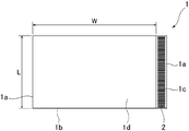
図2に、本発明に一実施形態の方法において使用することができる光学表示セル1の一例を示す。この光学表示セル1は平面形状が短辺1aと長辺1bとを有する長方形形状であり、一方の短辺1aに沿って所定幅の端子部分1cが形成されている。この端子部分1cには、電気接続のための多数の電気端子2が配置されている。光学表示セル1の端子部分2を除く領域が表示領域1dとなる。この表示領域1dは、横方向の幅Wと縦方向の長さLとを有する。本発明の方法を実施するためには、光学表示セル1は有機EL表示セルであることが好ましいが、矩形形状の1辺にのみ端子部分が形成された形式であれば、液晶表示セルであっても、本発明の方法を適用することができる。
FIG. 2 shows an example of an
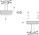
図3は、有機EL表示セルの製造工程の一例を概略的に示す斜視図であり、この工程においては、先ずガラス基板3が準備され、該ガラス基板3上に、耐熱性樹脂材料、好ましくはポリイミド樹脂が所定厚さに塗布され、乾燥されることによって、樹脂基材4が形成される。耐熱性樹脂材料としては、ポリイミド樹脂の他、ポリエチレンテレフタレート(PET)、ポリエチレンナフタレート(PEN)、ポリカーボネート(PC)などを使用することができる。その他に、基材の材料としては、特開2007−157501号公報(特許文献3)に記載されているような可撓性セラミックシート、或いは、特開2013−63892号公報(特許文献4)、特開2010−13250号公報(特許文献5)、特開2013−35158号公報(特許文献6)に記載されているような可撓性のガラスを使用することもできる。可撓性セラミックシート又は可撓性ガラスを基材として使用する場合には、ガラス基板3を使用する必要はない。
FIG. 3 is a perspective view schematically showing an example of a manufacturing process of an organic EL display cell. In this process, a glass substrate 3 is first prepared, and a heat-resistant resin material, preferably, is formed on the glass substrate 3. The
この樹脂基材4上に、複数の有機EL表示セル1が、周知の製造方法により、縦横の行列状に配列された状態で形成される。その後、樹脂基材4上に形成された有機EL表示セル1を覆うように、表面保護フィルム5が貼り合わされる。次いで、ガラス基板3が、レーザ照射等の公知の方法により、樹脂基材4から剥がされる。レーザ照射によりガラス基板を樹脂基材から剥がす技術は、例えば、国際公開公報WO2009/104371号(特許文献7)に記載されている。該ガラス基板3が剥がされた後の樹脂基材4に裏面保護フィルム6が貼り合わされる。本実施形態の説明において、セル集合体マザーボードBという用語は、表面保護フィルムを除く、樹脂基材4とその上に形成された表示セル1、及び裏面保護フィルム6からなる積層構造体を指すものとして使用される。
On this
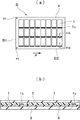
図4(a)は、表面保護フィルム5が貼り合わされていない、セル集合体マザーボードBを示す平面図であり、同図(b)は、図4のb−b線における断面図であるが、表面保護フィルム5が貼り合わされた状態のセル集合体マザーボードBを示す。図4(a)に示すように、セル集合体マザーボードBにおいては、複数の光学表示セル1が、端子部分1aが横方向に向けられる状態で、縦方向の列及び横方向の行を構成するように、行列配置される。セル集合体マザーボードBは、図4(a)に示すように、短辺B−1と長辺B−2とを有する矩形形状であり、一方の短辺B−1の両端近傍にマザーボードBの基準点となる基準標識mが、印字、刻印その他の適当な手法により付されている。光学フィルムの貼り合わせに際しては、セル集合体マザーボードBは、図4(a)に矢印Aで示す方向、すなわち縦方向に送られる。
FIG. 4 (a) is a plan view showing the cell assembly mother board B where the surface
図5及び図6に、位置調節ステーションIの構成を示す。図5は、位置調節ステーションIにおける貼り合わせ前のマザーボード位置調節段階を示す概略図である。図4(a)に示すセル集合体マザーボードBは、表面保護フィルム5が貼り合わされた状態でマザーボード搬送台7に載置され、矢印Aで示す送り方向に送られて、マザーボード位置調節盤8の下方位置に達する。マザーボード位置調節盤8は、下面に多数の吸引用孔(図示せず)を有し、内部が真空吸引装置(図示せず)に接続された真空吸引盤として構成されており、上下方向に移動可能な構成である。さらに、該マザーボード位置調節盤8は、送り方向に対し、横方向及び縦方向に可動に支持され、かつ、回転位置すなわち方位方向に位置調節可能な構成である。
5 and 6 show the configuration of the position adjustment station I. FIG. FIG. 5 is a schematic view showing a mother board position adjusting stage before bonding in the position adjusting station I. The cell assembly mother board B shown in FIG. 4 (a) is placed on the mother board carrier 7 with the surface
マザーボード搬送台7に載置されたセル集合体マザーボードBがマザーボード位置調節盤8の下方の位置に達すると、該マザーボード位置調節盤8は、図5(a)に示すように、その下面がマザーボード搬送台7上のセル集合体マザーボードBの表面保護フィルム5に接触するまで下方に移動し、その位置で真空吸引装置が作動して、真空吸引力により、セル集合体マザーボードBを吸着する。その状態でマザーボード位置調節盤8は、マザーボード搬送台7から上方に上昇し、図5(b)に示すマザーボード位置検出部に送られる。マザーボード位置検出部には、マザーボードB上の基準標識mを読み取るための光学的読み取り装置9が配置されており、この装置9がマザーボードB上の基準標識mを読み取って該マザーボードBの位置を判断する。
When the cell assembly mother board B placed on the mother board carrier 7 reaches a position below the mother board
図5(c)は、セル集合体マザーボードBの読み取られた位置APと、該マザーボードBの基準位置RPとを例示的に示す概略図である。読み取り位置APと基準位置RPとの対比により、左右の基準標識mの位置における横方向の変位量d1、d2及び縦方向の変位量d3、d4を演算し、演算された変位量を記憶手段(図示せず)に記憶する。次いで、マザーボード位置調節盤8は、貼合せ用吸引保持盤10が待機する転載位置に送られる。
FIG. 5C is a schematic diagram exemplarily showing the read position AP of the cell assembly motherboard B and the reference position RP of the motherboard B. By comparing the reading position AP and the reference position RP, the horizontal displacements d1 and d2 and the vertical displacements d3 and d4 at the positions of the left and right reference signs m are calculated, and the calculated displacements are stored in the storage means ( (Not shown). Next, the mother board
図6は、転載位置における動作を示す概略図である。転載位置において、マザーボード位置調節盤8は、演算され記憶手段に記憶されていた変位量d1、d2、d3、d4に基づき、該変位量が零になるように、マザーボード位置調節盤8の縦横方向位置及び回転方位を調節する。貼合せ用吸引保持盤10は、図7に平面図で示されるように、短辺10a及び長辺10bを有する長方形形状であり、一方の短辺の両端部近傍に、基準点を示すための一対の基準標識nが、印刷、刻印、その他の適当な手段により形成されている。転載位置には、この貼合せ用吸引保持盤10の基準標識nを読み取って、該貼合せ用吸引保持盤10の位置を検出する光学的読み取り装置11が配置されている。
FIG. 6 is a schematic diagram showing the operation at the transfer position. At the transfer position, the mother board
図7に示すように、貼合せ用吸引保持盤10に上面には多数の吸引用孔10aが縦横の行列状に形成されており、これら吸引用孔10aは、貼合せ用吸引保持盤10の内部空洞を通って真空吸引装置(図示せず)に接続されている。図7に破線12で示されるのは、該貼合せ用吸引保持盤10上におけるセル集合体マザーボードBの基準位置である。マザーボード位置調節盤8と同様に、貼合せ用吸引保持盤1貼合せ用吸引保持盤10も横方向及び縦方向の位置調節と回転方向の方位角調節が可能なように支持されている。そして、転載位置において、貼合せ用吸引保持盤10は、その基準標識nの位置が光学的読み取り装置11により読み取られ、セル集合体マザーボードBの位置調節に関連して述べたのと同様にして、基準位置に位置調節される。この状態では、転載位置において基準位置に調節されたセル集合体マザーボードBは、基準位置に調節された貼合せ用吸引保持盤10の破線12に対し上方に位置整合した状態になる。
As shown in FIG. 7, a large number of suction holes 10 a are formed in a vertical and horizontal matrix on the upper surface of the bonding
この状態で、セル集合体マザーボードBを保持するマザーボード位置調節盤8は、セル集合体マザーボードBの下面が貼合せ用吸引保持盤10の上面に接触するまで下方に移動させられる。次いで、貼合せ用吸引保持盤10に接続された真空吸引装置が作動させられ、同時に、マザーボード位置調節盤8に接続された真空吸引装置の作動が停止される。その結果、セル集合体マザーボードBは、貼合せ用吸引保持盤10上の破線12により示される基準位置に位置決めされて、該貼合せ用吸引保持盤10上に真空吸引保持される状態になる。換言すると、セル集合体マザーボードBは、マザーボード位置調節盤8から貼合せ用吸引保持盤10に転載される。その後、セル集合体マザーボードBを解放したマザーボード位置調節盤8は、貼合せ用吸引保持盤10から離れて上方に移動し、同様な動作を繰り返す。
In this state, the mother board
セル集合体マザーボードBを所定位置に保持する貼合せ用吸引保持盤10は、次に表面保護フィルム剥離ステーションIIに送られる。図9は、表面保護フィルム剥離ステーションIIにおける剥離装置の構成を示す概略図である。貼合せ用吸引保持盤10は、上述した横方向及び縦方向の位置と回転方位の調節が可能なように支持機構13により支持されており、該支持機構13は、貼合せ用吸引保持盤10を上下方向に昇降させることができるように、昇降機構(図示せず)を備える。該支持機構13は、ガイドレール14に沿って走行するガイド15に支持されており、該ガイド15は、リニアモータ(図示せず)を有する自走式装置として構成することができる。
The adhering
表面保護フィルム剥離ステーションIIにおいては、剥離用粘着テープ駆動装置16が、ガイドレール14の上方に配置されている。剥離用粘着テープ駆動装置16は、テープ繰り出しロール16aと、テープ巻き取りロール16bと、一対の押圧ロール16cとを備え、これらのロールは、剥離用粘着テープ16dが、テープ繰り出しロール16aから繰り出され、粘着面を下向きにした状態で一対の押圧ロール16cの下側を通って巻き取りロール16bに達するように配置される。一対の押圧ロール16cは、繰り出しロール16a及び巻き取りロール16bより下方の所定高さにおいて、ガイドレール14の延びる方向、すなわちセル集合体マザーボードBの送り方向に間隔をもって配置される。図には示していないが、これらの押圧ロール16は、弾性手段例えばバネにより下向きに付勢されるようにすることが好ましい。
In the surface protective film peeling station II, the peeling adhesive
ガイド15及び支持機構13に支持された貼合せ用吸引保持盤10上のセル集合体マザーボードBは、図9(a)に示す位置で表面保護フィルム剥離位置に送り込まれ、図9(b)に示す位置において昇降機構により所定高さまで上昇させられる。この所定高さは、セル集合体マザーボードBの表面保護フィルム5の上面が、一対の押圧ロール16c間に位置する粘着テープ16dに所定の接触圧で接触できる高さである。
The cell assembly mother board B on the
昇降機構により所定高さまで上昇させられたセル集合体マザーボードBは、そのまま剥離用粘着テープ駆動装置16の下方の位置に送られる。ここで、マザーボードBの表面保護フィルム5の上面が、一対の押圧ロール16cの間において粘着テープ16dの粘着面に押圧状態で接触する。粘着テープ16dの表面保護フィルム5に対する接着力は、表面保護フィルム5の光学表示セル1に対する接着力よりも大きく、したがって、表面保護フィルム5は、粘着テープ16dに付着して、樹脂基材4上に配置された光学表示セル1から剥離される。剥離された表面保護フィルム5は、巻き取りロール16bにより粘着テープ16dとともに巻き取られる。表面保護フィルム5が剥離されたマザーボードBは、図9(d)に示す位置において昇降機構により、図9(a)の位置における送り込み時の高さまで下降させられて、次工程に送られる。
The cell assembly mother board B raised to a predetermined height by the elevating mechanism is sent to a position below the peeling adhesive
図10は、剥離用粘着テープ駆動装置16の具体的構成の一例を示す斜視図であり、図9に側面図で示すテープ駆動装置16が二組、並列に配置される。図の表示を複雑にしないために、図10においては、表示のために必要な要素のみを示し、表示セル等は省略してある。表面保護フィルム5の剥離は、図9及び図10に示すような剥離用粘着テープを使用する形式に限らず、例えば表面保護フィルムの送り方向前側角部を、例えば粘着ロールにより少し剥がし、この剥がした角部を例えばクランプにより挟んで斜め後方に引くことにより、剥離する等の、他の剥離機構を採用することも可能である。
FIG. 10 is a perspective view showing an example of a specific configuration of the peeling adhesive
表面保護フィルム剥離工程に続く工程は、表面検査工程である。表面保護フィルム剥離ステーションIIから送り出された貼合せ用吸引保持盤10上のセル集合体マザーボードBは、ガイドレール14に沿って走行するガイド15により、第1表面検査ステーションIIIに送られる。この時のセル集合体マザーボードBは、樹脂基材4上に形成された表示セル1が露出された状態にある。この表示セル1に対し、光学的に表面検査が行われる。図1に例示的に示すように、第1表面検査ステーションIIIには表面検査のための光を照射する光源17と、被検査体である表示セル1により反射された光を受光する受光素子18が備えられている。検査を終えたセル集合体マザーボードBは、貼合せ用吸引保持盤10上に支持された状態で、次工程のために偏光子積層体貼合せステーションIVに送られる。
The process following the surface protective film peeling process is a surface inspection process. The cell assembly mother board B on the bonding
図11に貼合せステーションIVの一例を示す。集合体マザーボードBを載置した貼合せ用吸引保持盤10は、ガイドレール14に沿って走行するガイド15により、第1表面検査ステーションIIIから貼合せステーションIVに送られる。貼合せステーションIVには、マザーボード位置検出装置19が設けられており、該マザーボード位置検出装置19は、貼合せステーションIVに送り込まれたマザーボードBの基準標識mnを光学的に読み取ってマザーボードBの位置情報を生成する。この位置情報は、図11には示されていない制御装置の記憶部に記憶される。次いで、集合体マザーボードBを載置した貼合せ用吸引保持盤10は、貼合せ位置に移動させられ、支持機構13の昇降機構により、所定の貼合せ高さまで上昇させられる。制御装置は、貼合せ用吸引保持盤10の支持機構13及びガイド15の作動を制御する。
FIG. 11 shows an example of the bonding station IV. The laminating
貼合せステーションIVには貼合せ機構20が備えられている。貼合せ機構20は、長尺の光学フィルム21をロール状に巻いた光学フィルムロール22を備える。光学フィルム21は、一対の駆動ロール23により光学フィルムロール22から一定の速度で繰り出される。本実施形態においては、光学フィルム21は、偏光子21aの両側にTACフィルムのような保護フィルム21bが貼り合わされた長尺ウェブ状の偏光フィルムと粘着剤層21dを介して該偏光フィルムに接合された長尺ウェブ状の1/4波長(λ)位相差フィルム21cとからなる積層構成である。該位相差フィルム21cの外側には、別の粘着剤層21dを介してキャリアフィルム21eが貼り合わされる。偏光子21aと位相差フィルム21cとは、該偏光子21aの吸収軸と位相差フィルム21cの遅相軸又は進相軸とが45°±5°の範囲の角度で交差するように配置する。この光学フィルム21は、長尺の連続ウェブ形状であるが、その幅は、マザーボードB上に配置された各表示セルの横方向幅Wに対応する寸法である。
A
本実施形態の場合、偏光子21aの吸収軸は、該偏光子21aの長さ方向に平行とし、位相差フィルム21cの遅相軸が、該位相差フィルム21cの長さ方向に対して45°±5°の範囲の角度だけ斜め方向に向いた構成とする。このためには、位相差フィルム21cの製造段階で、該フィルムを斜め延伸する必要がある。この斜め延伸に関しては、特願2013−070787号(特許文献8)、特願2013−070789号(特許文献9)に詳細な記載があり、これらの文献に記載された方法により延伸された位相差フィルムを使用することができる。また、位相差フィルム21cとして、位相差が波長に応じて短波長側ほど小さくなる逆分散特性をもったフィルムを使用することができる。逆分散特性を有する位相差フィルムは、特許第5204200号(特許文献10)、特許第5448264号(特許文献11)等に記載があり、本実施形態の方法においては、これらの特許出願に記載された逆分散特性の位相差フィルムを使用することができる。
In this embodiment, the absorption axis of the
さらに図11を参照すると、一対の駆動ロール23により光学フィルムロール22から繰り出された光学フィルム21は、ガイドロール24、上下方向に可動なダンサーロール25及びガイドロール26及びガイドロール27を経て切り込み形成機構28に送られる。切り込み形成機構28は、切断刃29と送り出し用の一対の駆動ロール30とからなる。この切り込み形成機構28は、切り込み形成位置において駆動ロール30を停止させ、光学フィルム21の送りを停止させた状態で、切断刃29を作動させ、キャリアフィルム21eを残して光学フィルム21のみに、その幅方向に切り込み28aを形成する。切り込み28aの間隔は、マザーボードB上の各表示セル1の縦方向の長さLに対応する距離である。したがって、光学フィルムは、切り込み28aにより幅方向に切断されて、表示セルの横方向幅Wと縦方法長さLを有する光学フィルムシート21fとなる。このようにして、キャリアフィルム21e上には、複数の光学フィルムシート21aが連続的に形成され、これらの光学フィルムシート21aは、キャリアフィルム21eに支持されて貼合せ位置に送られる。
Referring further to FIG. 11, the
ダンサーロール25は、上向きに弾性的に付勢されており、連続的に光学フィルム21を送り方向に駆動する一対の駆動ロール23と、切断時には光学フィルム21の送りを停止し、切断終了後に所定距離だけ駆動を行う一対の駆動ロール30との間でフィルム送りの調整を行うように作用する調整ロールである。すなわち、駆動ロール30の停止期間においては、ダンサーロール25は、付勢力により駆動ロール23の送り分を吸収するように上方に移動し、駆動ロール30の作動が開始されたときに、該駆動ロール30により光学フィルム21に加えられる引張力により、付勢力に抗して下方に移動する。
The
切り込み28aにより形成された一連の光学フィルムシート21fは、キャリアフィルム21eに支持された状態で、ガイドロール31、及びガイドロール32を経て、ダンサーロール25と同様な構成のダンサーロール33を通り、ガイドロール34、35、36、37により案内されて貼合せ位置に送られる。
A series of
貼合せ位置には、貼合せロール38とキャリアフィルム剥離機構39が備えられている。貼合せロール38は、上方の引込み位置と下方の押圧位置との間を可動に配置されており、キャリアフィルム21eに支持された連続する光学フィルムシート21fのうち、先頭の光学フィルムシート21fの先端が、貼合せ対象の表示セル1の先端に位置整合した状態になったとき、上方位置から下方の押圧位置まで下降して、光学フィルムシート21fをマザーボードB上の表示セル1に押し付けて貼り合わせを行う。
A
キャリアフィルム剥離機構39は、貼合せ位置において、キャリアフィルム21eを鋭角に折り返して、先頭の光学フィルムシート21fを該キャリアフィルム21eから剥がすように作用する剥離ブレードを備える。鋭角に折り返されたキャリアフィルム21eを引き取るためにキャリアフィルム巻き取りロール40が配置される。光学フィルムシート21fから剥がされたキャリアフィルム21eは、ガイドロール41及び一対の巻き取り用駆動ロール42を経て、巻き取りロール40に送られ、該巻き取りロール40に巻き取られる。
The carrier
駆動ロール30及び切断刃29の作動は、図11には示していない前述した制御装置により制御される。すなわち、制御装置は、マザーボードB上の表示セル1の寸法及び位置に関する情報を格納しており、表示セル1の縦方向長さLの情報に基づいて制御装置が駆動ロール30の駆動と切断刃29の作動を制御して、表示セル1の縦方向長さLに対応する長さ方向間隔で、光学フィルム21に切り込み28aを形成する。また、貼合せ位置の上流側には、光学フィルムシート21fの先端を検出するフィルム検出装置43が設けられており、貼合せ位置に送られる光学フィルムシート21fの先端位置についての情報を制御装置に提供する。この光学フィルムシート先端位置情報は、制御装置に格納され、制御装置は、この光学フィルムシート先端位置情報と、貼合せ用吸引保持盤10から取得したマザーボードBの位置情報に基づき、駆動ロール30と巻き取り用駆動ロール42の作動を、貼合せ用吸引保持盤10の動きに対応させて制御し、キャリアフィルム21eから剥がされた光学フィルムシート21fの先端が、貼合せ位置にあるマザーボードB上の貼り合わせが行われる表示セル1の先端に位置整合するように調節する。位置整合が達成されると、光学フィルムシート21fとマザーボードBは、同期した速度で送られる。貼合せロール38が下方の押圧位置に下降して、光学フィルムシート21fを表示セル1の表示面に押し付ける。このようにして、表示セル1への光学フィルムシート21fの貼り合わせが行われる。
The operations of the
図13は、光学フィルムシート21fを、マザーボードB上において縦横の行列状に配列された表示セル1に順次は貼り合わせる順序の一例を示す概略図である。この例においては、貼合せ機構20は、送り方向に対する横方向位置が固定されており、マザーボードBを保持する貼合せ用吸引保持盤10は、支持機構13上に横方向移動が可能なように取り付けられている。図13(a)に示すように、マザーボードBの位置は、最初に左端の表示セル列の先頭の表示セル1が貼合せ位置に位置決めされるように制御される。この状態で、図11に関連して前述したように、光学フィルムシート21fが左端列先頭の表示セル1の表示部1dに貼り合わされる。
FIG. 13 is a schematic diagram illustrating an example of an order in which the
次いで、貼合せ用吸引保持盤10を横方向に動かすことにより、マザーボードBが送り方向に対して左横方向に、表示セル列の横方向間隔に相当する距離だけ変位させられる。この横変位により、図13(b)に示すように、左から2番目の列の先頭の表示セル1が貼合せ位置に位置決めされる。そして、前述と同様の動作により、この表示セル1の表示部1dに光学フィルムシート21fが貼り合わされる。その後、同様の操作によりマザーボードBが左横方向に変位させられて、光学フィルムシート21fの貼り合わせが行われる。表示セル1が3列に配置されている図示例の場合には、これで先頭の表示セルへの光学フィルムシート21fの貼り合わせは完了する。この状態を図13(c)に示す。
Next, by moving the laminating
次に、各縦列における表示セル1の間隔に相当する距離だけ貼合せ用吸引保持盤10が送り方向に駆動され、右端の列の先頭から2番目の表示セル1が貼合せ位置に位置決めされ、同様にして、図13(d)に示すように、このセル1の表示部1dに光学フィルムシート21fが貼り合わされる。その後、図13(e)に示すように、マザーボードBが送り方向に駆動されて、同様な操作により光学フィルムシート21fの貼合せが行われる。
Next, the bonding
すべての表示セル1に対する光学フィルムシート21fの貼合せが完了すると、マザーボードBは、貼合せ用吸引保持盤10上に保持された状態で第2表面検査ステーションVに送られる。第2表面検査ステーションVの構成は、第1表面検査ステーションIIIの構成と同様であり、検査用の光源44と反射光を受けるための受光素子45とを有する。第2表面検査ステーションVにおいて表面検査が行われたマザーボードBは、該第2表面検査ステーションVから切断ステーションVIに送られる。
When the bonding of the
図14は、切断ステーションVIにおいて使用される切断装置の一例を示す斜視図である。切断装置は、内部が真空吸引源49に接続された真空吸引台46と、該真空吸引台46上に取り外し可能に取り付けられた切断用型板47とを備える。表示セル1の寸法及びマザーボードB上における表示セル1の配列間隔に対応する間隔で形成された切断用溝47aを有する。さらに、切断用型板47は、貼合せ用吸引保持盤10と同様に、多数の真空吸引孔47bを有する。また、これらの切断用溝47aに沿って移動することにより切断用型板47上に置かれた物体を縦横の所定寸法に切断するための切断刃48が設けられる。この切断用型板47は、表示セル1の寸法に適合する複数のものが準備されており、切り出される表示セルの寸法に応じて適切なものを選んで真空吸引台45に取り付けて使用することができる。
FIG. 14 is a perspective view showing an example of a cutting device used in the cutting station VI. The cutting device includes a vacuum suction table 46 that is connected to a
切断ステーションVIに移送されたマザーボードBは、貼合せ用吸引保持盤10から真空吸引台45上の切断用型板47上に転載される。この転載は、位置調節ステーションIに関連して前述した転載と同様の方法により行うことができる。切断用型板47上に位置決めされて真空保持されたマザーボードBは、切断用型板47の切断用溝47aに沿って切断刃48を移動させることにより、個々の表示セル1に対応する寸法に切断される。このようにして、光学フィルムシート21fが表示部1dに貼り合せられた表示セルが得られる。
The mother board B transferred to the cutting station VI is transferred from the bonding
切断は、図14に示すような切断刃48によるものに限られず、例えば、図1の切断ステーションVIに例示的に示すレーザ切断機構50又は多数の切断刃を備えた打ち抜き機構51によって切断を行ってもよい。切断された個々の表示セル1は、例えば図15に示すような真空吸引式の搬送機構52によって次工程に搬送することができる。
The cutting is not limited to the cutting with the
上述した実施形態においては、キャリアフィルム21eに支持された積層構成の光学フィルムは、予め切断機構28により所定の長さに切断されて光学フィルムシート21fの形態にされ、その後でマザーボードB上の表示セル1の表示部1dに貼り合わされたが、本発明の他の態様においては、予めシート上に切断されることなく、光学フィルムは、連続帯状フィルムの形態で、縦列の表示セルの全体に渡して貼り合わされる。この実施形態では、図11に示す貼合せ機構20における切り込み形成機構28は必要でない。この実施形態による貼合せを図16に示す。図16(a)に示すように、マザーボードBは、送り方向左端の列の先頭の表示セル1の先端が貼合せ位置における所定の位置に位置決めされる。図13に関連して上述したように、光学フィルム21からキャリアフィルム21eを剥がして、該光学フィルムを左端列の表示セル1に連続的に貼り合わせる。次いで、マザーボードBを左横方向及び後方に移動させて、図16(b)に示すように2列目先頭の表示セル1が貼合せ位置に整合する状態にして、同様な貼り合わせを行う。同様に、マザーボードBを左横方向及び後方に移動させて、図16(b)に示すように右端列先頭の表示セル1が貼合せ位置に整合する状態にして、同様な貼り合わせを行う。このようにして貼り合わせが行われたマザーボードBは、図14に示す切断機構により切断を行って個々の表示セル1を得る。この切断により、連続的に貼り合わされた光学フィルム21は、表示セルの表示面1dの寸法に対応する寸法に切断される。
In the above-described embodiment, the laminated optical film supported by the
本発明の方法は、マザーボードB上に縦1列に配置された表示セル1への光学フィルムの貼り合わせにも適用することができる。その一例を図17に示す。この場合において、表示セル1は、端子部分1cが列の向きに対して横向きになるように、マザーボードB上に配置される。貼り合わせは、図11に関連して説明した動作を同様な動作により、列の先頭から順に、予め切断した光学フィルムシート21fを、表示セル1の表示部1dに貼り合わせることによって行うことができる。代替的には、列の表示セル1全体にわたって、その表示部1dに光学フィルム21を貼り合わせ、後の切断工程において、光学フィルム21の余剰部分を切り落としてもよい。
The method of the present invention can also be applied to the bonding of an optical film to the
図18及び図19は、本発明の方法を、比較的大きいサイズの柔軟性シート構造の表示セルに対する光学フィルムの貼り合わせに適用した実施形態を示すものである。表示セルが有機ELセルである場合には、セル自体を薄い厚みの柔軟性シート構造とすることができる。このような柔軟性シート構造の光学表示セルの場合、その薄さと柔軟性のために、通常のロール・ツー・パネル(RTP)技術により光学フィルムの貼り合わせを行うことは困難である。本発明のこの実施形態によれば、上述した方法を用いて、比較的大きいサイズの柔軟性シート構造の光学表示セルに対する光学フィルムの貼り合わせを行うことができる。 18 and 19 show an embodiment in which the method of the present invention is applied to bonding of an optical film to a display cell having a relatively large size flexible sheet structure. When the display cell is an organic EL cell, the cell itself can have a thin flexible sheet structure. In the case of an optical display cell having such a flexible sheet structure, it is difficult to bond optical films by a normal roll-to-panel (RTP) technique because of its thinness and flexibility. According to this embodiment of the present invention, an optical film can be bonded to an optical display cell having a flexible sheet structure having a relatively large size using the method described above.
図18を参照すると、柔軟性シート構造の光学表示セル60は、短辺60aと長辺60bとを有する矩形形状で、短辺60aに沿って位置する端子部分60cと、縦方向の長さLと横方向の幅Wとを有する表示部60dとを有する。この表示セル60は、製造段階で、ポリイミドのような耐熱樹脂材料からなる基材61上に形成される。製造工程は、図3について説明した工程と同様であり、ガラス基板上に樹脂基材61がフィルム状に形成され、その上に、例えば有機EL表示セルのような光学表示セル60が形成される。図3の場合と異なる点は、本実施形態においては、基材61上に一つの表示セルが形成されることである。図3に関連して述べた工程におけると同様に、基材61上に光学表示セル60が形成された後、該表示セル60の上面に表面保護フィルムが貼り合わされ、次いで、基材61がガラス基板から剥がされる。その後、基材61の裏面にも保護フィルムが貼り合わされて、セルマザーボードBが形成される。このセルマザーボードBは、図5、図6、図7、図8、図9、図10に関連して説明された工程と同様の工程を経て、貼合せ用吸引保持盤10に保持された状態で、貼合せステーションIVに送られる。
Referring to FIG. 18, an
本実施形態においては、図11に示す貼合せ機構20と同様の機構を採用することができる。この場合、光学フィルムロール22から繰り出された光学フィルム21は、図18に示す表示セル60の幅Wに対応する幅を有する。図19に、貼合せ部の構成を概略的に示す。貼合せ部における作用は、図11について前述したものと同様である。
In the present embodiment, a mechanism similar to the
また、図16を用いて説明される実施態様では、光学フィルムが表示セルに対して縦方向に貼り合わされたが、本発明のさらに別の態様では、横方向に光学フィルムシートが貼り合わされる。図20は、この実施態様による貼り合わせの概略図を示す。図20に示すとおり、本態様では、送り方向72に端子部分が位置するように、表示セルが行列状に配置される。すなわち、本実施形態では、送り方向72が、表示セルの横方向、送り方向72に対して垂直の方向が表示セルの縦方向となる。また、本実施態様では、縦方向に並べられた表示セルの列70全体に対して、横方向に光学フィルムシート21fを貼り合わせるため、光学フィルム21の幅は、縦方向に並べられた表示セルの列70の縦寸法に対応する。ここで、表示セルの列70の縦寸法に「対応する」とは、厳密に一致することを意味するのではなく、表示セルの列70の縦寸法を含み、概ね一致すればよく、例えば、該縦寸法を基に光学フィルムの幅が定められればよい。本態様においては、光学フィルム21は、切り込み形成機構28によって、キャリアフィルム21eを残して、切断されて、光学フィルムシート21fが形成される。切断の間隔は、表示セル1の表示面1dの横方向幅Wに対応する。したがって、光学フィルム21は、切り込み28aにより幅方向に切断されて、表示セル1の表示面1dの横方向幅Wと表示セル1の列70の全体の縦方向長さに対応する辺の長さを有する光学フィルムシート21fとなる。
In the embodiment described with reference to FIG. 16, the optical film is bonded to the display cell in the vertical direction. However, in still another aspect of the present invention, the optical film sheet is bonded in the horizontal direction. FIG. 20 shows a schematic view of bonding according to this embodiment. As shown in FIG. 20, in this aspect, the display cells are arranged in a matrix so that the terminal portions are positioned in the
図21は、図20に示される態様に関する貼り合わせ順序の一例を示す概略図である。貼合せ用吸引保持基板10を移動させて、図21(a)に示すように、1列目の表示セルの表示面1dの先端が、光学フィルムシート21fの先端である貼合せ位置に位置決めされる。粘着剤層21dが光学フィルムシート21f側に残るように、光学フィルムシート21fからキャリアフィルム21eを剥がして、該光学フィルムシート21fを1列目の表示セル1の表示面1dに横方向に連続的に貼り合わせる。次いで、マザーボードBを前方に移動させて、図21(b)に示すように2列目の表示セル1が、貼合せ位置に整合する状態にして、同様の貼り合わせを行う。同様に、マザーボードBを前方に移動させて、図21(c)に示すように3列目の表示セル1が貼合せ位置に整合する状態にして、同様の貼り合わせを行う。このようにして貼り合わせが行われたマザーボードBは、図14に示す切断機構により切断を行って個々の表示セル1を得る。この切断により、連続的に貼り合わされた光学フィルムシート21fは、表示セルの表示面1dの寸法に対応する寸法に切断される。本実施形態では、マザーボードBは、前方に移動するのみであり、マザーボードBを前後に移動させる必要がないから、マザーボード上に行列状に配置された多数の表示セルを短い時間で貼り合わせることができる。縦方向に光学フィルムを貼合せる多数の貼合せ機構を用いることによっても、前方への移動のみで、マザーボード上の全ての表示セルに貼り合わせを行うことは、可能であるが、多数の貼合せ機構を用いると、設備の占有面積が拡大するし、1つでも貼合せ機構が、故障すると、貼り合わせ装置全体を停止させることになるため、稼働が不安定となる。また、多数の貼合せ機構は、製造装置のコストを増加させることになる。なお、図21に示される実施形態においては、貼合せ方法を除いては、図11に示される実施形態と同様である。
FIG. 21 is a schematic diagram illustrating an example of a bonding order regarding the aspect illustrated in FIG. 20. As shown in FIG. 21 (a), the tip of the display surface 1d of the display cell in the first row is positioned at the bonding position, which is the tip of the
また、図20に示された実施態様では、貼合せを行う前に、光学フィルム21を、表示面1dの横方向幅に切断して、光学フィルムシート21fを形成したが、本発明のさらに別の実施態様においては、光学フィルム21を表示セル1の表示面1dに横方向に連続的に貼合せた後に、光学フィルム21の切断を行い、光学フィルムシート21fを形成する。表示セル1の横方向の後方端部に一致させて、光学フィルム21の切断を行ってもよいが、後の切断ステーションVIでの切断工程で光学フィルムシート21fの余剰部分を切除することができるので、光学フィルム21の余剰部分を残して、表示面1dの後方端部近辺で切断してもよい。横方向の後方に端子部分1cが存在すると端子部分1c上で光学フィルム21を切断することになり、端子部分1cを損傷させやすいので、端子部分1cは、横方向の先端側に位置するように配置することが望ましい。
Further, in the embodiment shown in FIG. 20, the
また、本発明の別の態様においては、光学フィルムシートが、表示セルの横方向に貼り合わされる点では、図20に示される実施態様と同一であるが、複数の光学フィルムロールを用いる点で異なる。図22に、この態様による貼り合わせの概略図を示す。本実施形態では、二つの光学フィルムロール22−1及び22−2の幅はそれぞれ、表示セルの列70を構成する表示セルの二つの部分列70−1及び70−2の縦方向寸法に対応し、二つの光学フィルムロール22−1及び22−2の全体の幅が、表示セルの列70の縦方向寸法に対応する。本態様においても光学フィルム21−1及び21−2は、切り込み形成機構28により、キャリアフィルム21e−1及び21e−2を残して切断されて、光学フィルムシート21f−1及び21f−2が形成される。切断の間隔は、表示セル1の表示面1dの横方向幅Wに対応する。したがって、光学フィルム21−1及び21−2は、切断によって、表示セル1の表示面1dの横方向幅Wと表示セル1の部分列70−1(70−2)の縦方向長さに対応する辺を有する光学フィルムシート21f−1及び21f−2となる。本態様においては、同一の光学フィルムロールを2本用いているが、3本等の他の本数のフィルムロールを用いてもよいし、異なる幅の光学フィルムロールを用いてもよい。また、一つの光学フィルムロールを用いる場合と同様に、光学フィルムを表示セルに貼り合わせた後に、光学フィルムを切断するように構成してもよい。
Moreover, in another aspect of the present invention, the optical film sheet is the same as the embodiment shown in FIG. 20 in that the optical film sheet is bonded in the lateral direction of the display cell, but a plurality of optical film rolls are used. Different. In FIG. 22, the schematic of the bonding by this aspect is shown. In the present embodiment, the widths of the two optical film rolls 22-1 and 22-2 correspond to the vertical dimensions of the two partial columns 70-1 and 70-2 of the display cells constituting the
図23は、図22に示される態様に関する貼り合わせ順序の一例を示す概略図である。貼り合わせは、図20に記載の態様と同様の貼合せ方法によって行われる。すなわち、マザーボードBを前方(横方向)に移動させて、図23(a)に示すように、光学フィルムシート28−1の先端が、1列目の表示セル1の表示面1dの先端に合うように位置決めされて、部分列70−1に属する表示セル1に対する貼り合わせが行われる。貼り合わせは、図13に関連して上述したように、光学フィルムシート21f−1からキャリアフィルム21e−1を剥がして、該光学フィルムシート21f−1を部分列70−1の1列目の表示セル1の表示面1dに横方向に連続的に貼り合わせる。このとき、光学フィルムシート28−2の貼合せ位置は、横方向(送り方向)に2列分光学フィルムシート28−1よりも送り先側に位置するため、部分列70−2に属する表示セル1には、光学フィルムシート21f−2の貼り合わせは行われない。次いで、マザーボードBを前方に移動させて、図23(b)に示すように、2列目の部分列70−1の表示セル1が、光学フィルムシート28−1の貼合せ位置に整合する状態にして、同様の貼り合わせを行う。さらに、マザーボードBを前方に移動させて、図23(c)に示すように3列目の表示セル1が貼合せ位置に整合する状態にする。このとき、光学フィルムシート28−2の先端が、部分列70−2の1列目の表示セルの表示面1dの先端に位置整合することになるから、3列目の部分列70−1の表示セルと部分列70−2の1列目の表示セルは、同時に貼合せが行われることになる。さらに、マザーボードBを前方に移動させて、図23(d)に示すように、4列目の部分列70−1の表示セル1が、光学フィルムシート28−1の貼合せ位置に整合し、2列目の部分列70−2の表示セル1が、光学フィルムシート28−2の貼合せ位置に整合する状態にして、同様の貼り合わせを行う。このようにして全ての表示セルに対して光学フィルムシートの貼り合わせが行われたマザーボードBは、図14に示す切断機構により切断を行って個々の表示セル1を得る。上記の実施態様と異なり、貼合せ機構は、横方向に関して同一の位置に並べてもよい。もっとも、図22に図示されていないが、実際の貼合せ位置の周辺には、剥離手段や貼合せロールの支持部材等を有する貼り合せ機構が存在する。そのため、光学フィルムの貼合せ位置を、光学フィルムロールごとに横方向に異なるように配置することで、かかる貼合せ機構の配置スペースを確保しやすくなる。特に隣接する貼合せ機構が、配置スペースの確保のために問題となるため、隣接する光学フィルムロールに対応する貼合せ位置のみを横方向に異なるようにすることが好ましい。本実施態様では、光学フィルムロール22−1及び22−2の貼合せ位置が、横方向に2列分異なっているが、これに限定されることはなく、例えば、1列分だけ貼合せ位置が異なるようにしてもよい。
FIG. 23 is a schematic diagram illustrating an example of a bonding order related to the aspect illustrated in FIG. Bonding is performed by the same bonding method as that of the embodiment shown in FIG. That is, the mother board B is moved forward (lateral direction), and as shown in FIG. 23A, the tip of the optical film sheet 28-1 is aligned with the tip of the display surface 1d of the
本発明の他の態様においては、表示セルの部分列に対応する幅を有する光学フィルムロールを用いるが、光学フィルムシートの貼合せ位置とマザーボードとを縦方向に相対的に移動させて、光学フィルムシートの貼り合わせを部分列ごとに順次に行うことによって、一列分の表示セルに光学フィルムシートを貼り合わせる。すなわち、表示セルの部分列に、光学フィルムシートを貼り合わせた後に、表示セル(マザーボード)と、光学フィルムシートとを、表示セルの部分列に相当する距離だけ縦方向に相対的に移動させて、光学フィルムシートの貼合せが行われていない部分列を構成する表示セルの表示面の先端を、光学フィルムシートの貼合せ位置に整合させる。図24は、マザーボードBを移動させることによって、光学フィルムシート28fとマザーボードBとの縦方向の相対的移動を行う実施態様を示す。図24に示される態様では、光学フィルムロール22は、部分列70−1(70−2)の縦方向寸法に対応する。また、光学フィルム21は、切り込み形成機構28により、キャリアフィルム21eを残して、切断されて、光学フィルムシート21fが形成される。切断の間隔は、表示セル1の表示面1dの横方向幅Wに対応する。したがって、光学フィルム21は、切り込み28aにより幅方向に切断されて、横方向幅Wと表示セル1の部分列70−1(70−2)の縦方向長さに対応する辺を有する光学フィルムシート21fとなる。
In another aspect of the present invention, an optical film roll having a width corresponding to a partial row of display cells is used, but the optical film sheet is relatively moved in the vertical direction by moving the bonding position of the optical film sheet and the mother board. The optical film sheet is bonded to one row of display cells by sequentially performing sheet bonding for each partial column. That is, after the optical film sheet is bonded to the display cell partial row, the display cell (motherboard) and the optical film sheet are relatively moved in the vertical direction by a distance corresponding to the display cell partial row. The tip of the display surface of the display cell constituting the partial row where the optical film sheet is not bonded is aligned with the bonding position of the optical film sheet. FIG. 24 shows an embodiment in which the optical film sheet 28f and the mother board B are moved relative to each other in the vertical direction by moving the mother board B. In the aspect shown in FIG. 24, the
図25は、図24に示される態様に関する貼り合わせ順序の一例を示す概略図である。図25(a)に示すように、貼合せ用吸引保持盤10を移動させることによって、マザーボードBを移動させて、マザーボードB上に行列状に配列された1列目の表示セルを光学フィルムシート21fの貼合せ位置に合わせる。次いで、図25(b)に示されるように、表示セルの1列目の送り方向から見て左側の部分列70−1を光学フィルムシート21fの貼合せ位置に合わせる。つまり、部分列70−1に属する表示セル1の表示面1dの先端と光学フィルムシート28fの先端とを位置整合させる。そして、部分列70−1に属する表示セル1の表示面1dに光学フィルムシート28fを横方向に連続的に貼り合わせる。かかる貼り合わせの後に、マザーボードBを、部分列の縦方向の寸法だけ縦方向(送り方向左側)に移動させて、図25(c)に示されるように、1列目の送り方向から見て右側の部分列70−2に属する表示セルを、光学フィルムシートの貼合せ位置に合わせる。マザーボードBは、貼り合わせのために、横方向に移動しているため、マザーボードBは、縦方向のみならず、表示面1dの横方向幅Wだけ、後方(貼合せ方向とは逆方向)に移動することになる。次いで、部分列70−2に属する表示セル1に光学フィルムシート21fを貼り合わせる。光学フィルムシート28fを一列目の全ての表示セルに貼り合せたら、図25(d)マザーボードBを縦方向(送り方向右側)及び前方に移動させて、2列目の部分列70−1に属する表示セル1を貼合せ位置に合わせて、2列目の部分列70−1に属する表示セル1に光学フィルムの貼合せを行う。1列目と同様に、マザーボードBを移動させて、図25(e)に示されるように、2列目の部分列70−2に属する表示セルに光学フィルムシート28fを貼り合わせる。このようにして全ての表示セル1に光学フィルムシート28fの貼り合わせが行われたマザーボードBが、図14に示す切断機構により切断を行って個々の表示セル1を得る点は、他の形態と同様である。
FIG. 25 is a schematic diagram illustrating an example of a bonding order related to the aspect illustrated in FIG. As shown in FIG. 25A, by moving the
図26は、光学フィルムシートを移動させることによって、上記の縦方向の相対的移動を行う実施態様を示す。この実施態様では、貼合せ機構20を縦方向に可動できるように設計し、貼合せ機構20を縦方向に移動させることよって、光学フィルムの貼合せ位置を、貼り合わせ対象となる表示セルの先端側の位置に合わせる点以外は、図24及び図25に記載される態様と同様である。
FIG. 26 shows an embodiment in which the relative movement in the vertical direction is performed by moving the optical film sheet. In this embodiment, the
図27は、図26に示される態様に関する貼り合わせ順序の一例を示す概略図である。図27(a)に示されるように、マザーボードBを移動させて、マザーボードB上に行列状に配列された表示セル1の1列目の表示セル1の表示面1dの先端と光学フィルムシート28f先端である貼合せ位置とを横方向に関して位置整合させる。次いで、図27(b)に示されるように、また、貼合せ機構20の移動により、光学フィルムシート28fを縦方向に移動させることによって、光学フィルムシートの先端を一列目の部分列70−1に縦方向に関して位置整合させる。すなわち、部分列70−1に属する表示セルの表示面1dと光学フィルムシート28fの先端とを位置整合させる。そして、1列目の送り方向右側に位置する部分列70−1に光学フィルムシートを横方向に連続的に貼り合わせる。かかる貼り合わせの後に、貼合せ機構20の移動により光学フィルムシート21fを、部分列の縦方向の寸法だけ縦方向(送り方向左側)に移動させて、図27(c)に示されるように、1列目の送り方向左側の部分列70−2に属する表示セル1に貼合せ位置を合わせる。マザーボードBは、貼り合わせのために、横方向に移動しているため、マザーボードBは、表示面1dの横方向幅Wだけ、後方(貼合せ方向とは逆方向)に移動することになる。次いで、部分列70−2に属する表示セル1に光学フィルムシート28fを貼合せる。光学フィルムシート28fを一列目の全ての表示セルに貼合せたら、貼合せ機構20を縦方向(送り方向右側)に移動させ、かつ、マザーボードBを前方に移動させて、図27(d)に示されるように、2列目の部分列70−1を貼合せ位置に合わせ、2列目の部分列70−1に属する表示セルに光学フィルムの貼合せを行う。そして、1列目と同様に、マザーボードBを移動させて、図27(e)に示されるように、2列目の部分列70−2に属する表示セル1に光学フィルムシート28fを貼り合わせる。本形態では、マザーボードBを縦方向に移動させないため、貼合せステーションIVの縦方向の大きさを小さくすることができるため、省スペース化が可能になる。
FIG. 27 is a schematic diagram illustrating an example of a bonding order regarding the aspect illustrated in FIG. 26. As shown in FIG. 27A, the mother board B is moved, and the tip of the display surface 1d of the
図25及び図27に示される貼り合わせ順序は、各列の貼合せを、部分列70−1に属する表示セル1から行っているが、列によって異なる順番で貼合せを行ってもよい。例えば、2列目を、部分列70−2に属する表示セルから貼り合わせを行うことによって、1列目から2列目に列を移動する際に縦方向にマザーボードB或いは光学フィルムシートを移動させる必要がなくなる。すなわち、列間の光学表示フィルムと表示セルの位置整合を行う際に、縦方向の位置整合を省略することができる。また、図25及び図27に示される態様では、一列当たり6個の表示セル1で構成される列に対して、3個の表示セル1に対する貼り合わせを2度行うことによって、一列分の表示セル1に光学フィルムシート28fを貼り合わせたが、2個の表示セルに対する貼合せを3回おこなってもよい。また、1つの表示セルに対する貼合せを6回行ってもよく、表示面1d外に残った余剰の光学フィルムが存在しない場合には、切断ステーションVIにおいて、光学フィルムを切断する必要がなくなる。なお、いずれの形態においても、一列当たりの表示セルの個数は、複数であればよく、6個に限られない。
In the bonding order shown in FIG. 25 and FIG. 27, each column is bonded from the
なお、図20から26に示される実施形態において、貼合せステーションIV以外の構成は、図1から図16を用いて説明される実施形態と同様である。 In addition, in embodiment shown by FIGS. 20-26, structures other than bonding station IV are the same as that of embodiment demonstrated using FIGS. 1-16.
以上、本発明を特定の実施形態について図示し、説明したが、本発明は、図示の実施形態に限定されるものではなく、本発明の範囲は、特許請求の範囲の請求項によってのみ定まるものである。 Although the present invention has been illustrated and described with respect to specific embodiments, the present invention is not limited to the illustrated embodiments, and the scope of the present invention is defined only by the claims of the claims. It is.
I・・・位置調節ステーション
II・・・表面保護フィルム剥離ステーション
III・・・第1表面検査ステーション
IV・・・偏光子積層体貼合せステーション
V・・・第2表面検査ステーション
VI・・・切断ステーション
W・・・横方向の幅
L・・・縦方向の長さ
B・・・セル集合体マザーボード
1・・・光学表示セル
1a・・・短辺
1b・・・長辺
1c・・・端子部分
1d・・・表示部分
3・・・ガラス基板
4・・・基材
5・・・表面保護フィルム
6・・・裏面保護フィルム
7・・・マザーボード搬送台
8・・・マザーボード位置調節盤
10・・・貼合せ用吸引保持盤
10a・・・吸引用孔
12・・・セル集合体マザーボードの基準位置
20・・・貼合せ機構
21・・・光学フィルム
21a・・・偏光子
21c・・・1/4波長位相差フィルム
21e・・・キャリアフィルム
21f・・・光学フィルムシート
22・・・光学フィルムロール
28・・・切り込み形成機構
28a・・・切り込み
29・・・切断刃
38・・・貼合せロール
39・・・キャリアフィルム剥離機構
46・・・真空吸引台
47・・・切断用型板
47a・・・切断用溝
47b・・・真空吸引孔
48・・・切断刃
49・・・真空吸引源
I ... Position adjustment station
II ... Surface protection film peeling station
III ・ ・ ・ First surface inspection station
IV ... Polarizer laminate bonding station
V ... Second surface inspection station
VI ... cutting station W ... lateral width L ... longitudinal length B ...
Claims (34)
電気接続用の電気端子を備える端子部分が一辺に形成された長方形形状の光学表示セルの複数個を、前記端子部分を有する辺が横方向に位置し光学表示面が上に向けられた状態で、少なくとも縦方向に列状に並べて基材上に配列した構成のセル集合体マザーボードと、
前記セル集合体マザーボード上に縦方向の列状に配列された前記光学表示セルの、配列状態における、前記端子部分を除く横方向幅に対応する幅を有する偏光子の層を少なくとも含む光学フィルムに、粘着剤層を介してキャリアフィルムを貼り合わせた連続ウェブ形状の光学フィルム積層体をロール状に巻いた光学フィルム積層体ロールと、
を使用し、
複数の前記セル集合体マザーボードを順次、貼合せ位置に送る段階と、
前記光学フィルム積層体を該光学フィルム積層体ロールから繰り出して前記貼合せ位置に送る段階と、
繰り出された前記光学フィルム積層体の該光学フィルムと該粘着剤層に対し、前記セル集合体マザーボード上に縦方向の列状に配列された前記光学表示セルの配列状態における縦方向寸法に対応する長さ方向の間隔で、横方向に切り込みを順次に形成して、縦方向に隣接する2つの切り込みの間に、粘着剤層を介して前記キャリアフィルム上に支持された光学フィルムシートを形成する段階と、
前記貼合せ位置において、前記光学フィルム側に前記粘着剤層が残る状態で前記光学フィルムシートを前記キャリアフィルムから剥がし、剥がされた前記光学フィルムシートを、前記縦方向に移動する前記セル集合体マザーボード上の縦方向の列状に配列された個々の光学表示セルの前記端子部分を除く光学表示面の区域に順次に貼り合わせる段階と、
を含み、
前記セル集合体マザーボード上の前記縦方向の列状に配列された光学表示セルの、縦方向にみて先頭の光学表示セルに対する該光学フィルムシートの貼り合わせが行われる前に、送り方向に対する前記セル集合体マザーボードの横方向位置及び方位角度の調節を行って、前記光学表示セルが、前記貼合せ位置に送られる前記光学フィルムシートに対し横方向及び方位角度に関し位置整合させられるようにし、前記セル集合体マザーボードの送りと前記光学フィルムシートの送りを調節することにより、個々の光学フィルムのシートの先端と、該セル集合体マザーボード上の対応する光学表示セルの先端とが位置合わせされるようにする
ことを特徴とする方法。 It is a method of bonding an optical film sheet to a rectangular optical display cell in which a terminal portion having an electrical terminal for electrical connection is formed on one side,
A plurality of rectangular optical display cells each having a terminal portion having an electrical terminal for electrical connection formed on one side, with the side having the terminal portion positioned laterally and the optical display surface facing upward A cell assembly mother board having a configuration arranged on a base material in a row in at least the vertical direction;
An optical film including at least a layer of a polarizer having a width corresponding to a width in a horizontal direction excluding the terminal portion of the optical display cells arranged in a vertical row on the cell assembly motherboard. An optical film laminate roll in which a continuous web-shaped optical film laminate in which a carrier film is bonded via an adhesive layer is wound into a roll,
Use
Sequentially sending the plurality of cell assembly motherboards to a bonding position;
Unwinding the optical film laminate from the optical film laminate roll and sending it to the laminating position;
Corresponding to the vertical dimension in the arrangement state of the optical display cells arranged in a vertical row on the cell assembly motherboard with respect to the optical film and the adhesive layer of the optical film laminate that has been fed out. Cuts are sequentially formed in the horizontal direction at intervals in the length direction, and an optical film sheet supported on the carrier film is formed between two cuts adjacent in the vertical direction via an adhesive layer. Stages,
The cell assembly motherboard in which the optical film sheet is peeled off from the carrier film with the pressure-sensitive adhesive layer remaining on the optical film side at the laminating position, and the peeled optical film sheet is moved in the longitudinal direction. Sequentially pasting to the area of the optical display surface excluding the terminal portions of the individual optical display cells arranged in a vertical row above,
Including
The cells in the feeding direction before the optical film sheet is bonded to the first optical display cell in the vertical direction of the optical display cells arranged in the vertical row on the cell assembly motherboard. Adjusting the lateral position and azimuth angle of the assembly mother board so that the optical display cell is aligned with respect to the optical film sheet sent to the laminating position with respect to the lateral direction and azimuth angle; By adjusting the feeding of the assembly motherboard and the feeding of the optical film sheet, the leading edge of each optical film sheet is aligned with the leading edge of the corresponding optical display cell on the cell assembly motherboard. A method characterized by:
電気接続用の電気端子を備える端子部分が一辺に形成された長方形形状の光学表示セルの複数個を、前記端子部分を有する辺が横方向に位置し光学表示面が上に向けられた状態で、少なくとも縦方向に列状に並べて基材上に配列した構成のセル集合体マザーボードと、
前記セル集合体マザーボード上に縦方向の列状に配列された前記光学表示セルの、配列状態における、前記端子部分を除く横方向幅に対応する幅を有する偏光子の層を少なくとも含む光学フィルムに、粘着剤層を介してキャリアフィルムを貼り合わせた連続ウェブ形状の光学フィルム積層体をロール状に巻いた光学フィルム積層体ロールと、
を使用し、
複数の前記セル集合体マザーボードを順次、貼合せ位置に送る段階と、
前記光学フィルム積層体を該光学フィルム積層体ロールから繰り出して前記貼合せ位置に送る段階と、
前記貼合せ位置において、前記光学フィルム側に前記粘着剤層が残る状態で前記光学フィルムを前記キャリアフィルムから剥がし、剥がされた前記光学フィルムを、送り方向に移動する前記セル集合体マザーボード上の縦方向の列状に配列された複数の光学表示セルの前記端子部分を除く光学表示面の区域に連続的に貼り合わせる段階と、
前記光学フィルムが連続的に貼り合わされた前記セル集合体マザーボード上の複数の光学表示セルを個々のセルに切り離し、同時に、該光学表示セルの縦方向端部において、個々のセルに貼り合わされた前記光学フィルムを切断する段階と、
を含み、
前記セル集合体マザーボード上の前記縦方向の列状に配列された光学表示セルの、縦向にみて先頭の光学表示セルに対する該光学フィルムシートの貼り合わせが行われる前に、送り方向に対する前記セル集合体マザーボードの横方向位置及び方位角度の調節を行って、前記光学表示セルが、前記貼合せ位置に送られる前記光学フィルムシートに対し横方向及び方位角度に関し位置整合させられるようにし、前記セル集合体マザーボードの送りと前記光学フィルムシートの送りを調節することにより、個々の光学フィルムのシートの先端と、該セル集合体マザーボード上の対応する光学表示セルの先端と、が位置合わせされるようにする
ことを特徴とする方法。 It is a method of bonding an optical film sheet to a rectangular optical display cell in which a terminal portion having an electrical terminal for electrical connection is formed on one side,
A plurality of rectangular optical display cells each having a terminal portion having an electrical terminal for electrical connection formed on one side, with the side having the terminal portion positioned laterally and the optical display surface facing upward A cell assembly mother board having a configuration arranged on a base material in a row in at least the vertical direction;
An optical film including at least a layer of a polarizer having a width corresponding to a width in a horizontal direction excluding the terminal portion of the optical display cells arranged in a vertical row on the cell assembly motherboard. An optical film laminate roll in which a continuous web-shaped optical film laminate in which a carrier film is bonded via an adhesive layer is wound into a roll,
Use
Sequentially sending the plurality of cell assembly motherboards to a bonding position;
Unwinding the optical film laminate from the optical film laminate roll and sending it to the laminating position;
In the bonding position, the optical film is peeled off from the carrier film in a state where the pressure-sensitive adhesive layer remains on the optical film side, and the peeled optical film is moved vertically in the cell assembly motherboard that moves in the feeding direction. Continuously pasting to the area of the optical display surface excluding the terminal portion of a plurality of optical display cells arranged in a row of directions;
A plurality of optical display cells on the cell assembly mother board on which the optical film is continuously bonded are separated into individual cells, and at the same time, at the longitudinal ends of the optical display cells, the optical display cells are bonded to the individual cells. Cutting the optical film;
Including
The cells in the feeding direction before the optical film sheet is bonded to the first optical display cell in the vertical direction of the optical display cells arranged in the vertical row on the cell assembly motherboard. Adjusting the lateral position and azimuth angle of the assembly mother board so that the optical display cell is aligned with respect to the optical film sheet sent to the laminating position with respect to the lateral direction and azimuth angle; The leading edge of each optical film sheet and the leading edge of the corresponding optical display cell on the cell aggregate motherboard are aligned by adjusting the feeding of the assembly motherboard and the feeding of the optical film sheet. A method characterized by.
電気接続用の電気端子を備える端子部分が一辺に形成された長方形形状で可撓性の柔軟シート構造の光学表示セルを、前記端子部分を有する辺が横方向に位置し光学表示面が上に向けられた状態で樹脂基材上に配列した構成のセルマザーボードと、
前記セルマザーボード上に配列された前記光学表示セルの、配列状態における、前記端子部分を除く横方向幅に対応する幅を有する偏光子の層を少なくとも含む光学フィルムに、粘着剤層を介してキャリアフィルムを貼り合わせた連続ウェブ形状の光学フィルム積層体をロール状に巻いた光学フィルム積層体ロールと、
を使用し、
複数の前記セルマザーボードを順次、貼合せ位置に送る段階と、
前記光学フィルム積層体を該光学フィルム積層体ロールから繰り出して前記貼合せ位置に送る段階と、
繰り出された前記光学フィルム積層体の該光学フィルムと該粘着剤層に対し、前記セルマザーボード上の前記光学表示セルの配列状態における縦方向寸法に対応する長さ方向の間隔で、横方向に切り込みを順次に形成して、粘着剤層を介して前記キャリアフィルム上に支持された光学フィルムシートを形成する段階と、
前記貼合せ位置において、前記光学フィルム側に前記粘着剤層が残る状態で前記光学フィルムシートを前記キャリアフィルムから剥がし、剥がされた前記光学フィルムシートを、送り方向に移動する前記セルマザーボード上の前記光学表示セルの前記端子部分を除く光学表示面の区域に貼り合わせる段階と、
を含み、
前記セルマザーボード上の前記光学表示セルに対する該光学フィルムシートの貼り合わせが行われる前に、送り方向に対する前記セルマザーボードの横方向位置及び方位角度の調節を行って、前記光学表示セルが、前記貼合せ位置に送られる前記光学フィルムシートに対し横方向及び方位角度に関し位置整合させられるようにし、前記セルマザーボードの送りを調節することにより、個々の光学フィルムのシートの先端と、該セルマザーボード上の対応する光学表示セルの先端と、が位置合わせされるようにする
ことを特徴とする方法。 It is a method of bonding an optical film sheet to an optical display cell having a flexible flexible sheet structure in a rectangular shape in which a terminal portion including an electric terminal for electrical connection is formed on one side,
An optical display cell having a rectangular flexible flexible sheet structure in which a terminal portion having an electrical terminal for electrical connection is formed on one side, the side having the terminal portion is located in the horizontal direction, and the optical display surface is on the upper side A cell motherboard with a configuration arranged on a resin base material in a directed state;
The optical display cell arrayed on the cell motherboard has an optical film including at least a polarizer layer having a width corresponding to a width in a lateral direction excluding the terminal portion in an array state. An optical film laminate roll in which a continuous web-shaped optical film laminate bonded with a film is wound into a roll, and
Use
Sequentially sending a plurality of the cell motherboards to the bonding position;
Unwinding the optical film laminate from the optical film laminate roll and sending it to the laminating position;
With respect to the optical film and the pressure-sensitive adhesive layer of the optical film laminate that has been fed out, a cut is made in the horizontal direction at intervals in the length direction corresponding to the vertical dimension in the arrangement state of the optical display cells on the cell motherboard. Sequentially forming an optical film sheet supported on the carrier film via an adhesive layer;
In the bonding position, the optical film sheet is peeled off from the carrier film with the pressure-sensitive adhesive layer remaining on the optical film side, and the peeled optical film sheet is moved in the feeding direction on the cell motherboard. Bonding to the area of the optical display surface excluding the terminal portion of the optical display cell;
Including
Before the optical film sheet is attached to the optical display cell on the cell motherboard, the lateral position and azimuth angle of the cell motherboard with respect to the feeding direction are adjusted, and the optical display cell is attached to the optical display cell. The optical film sheet sent to the alignment position is aligned with respect to the lateral direction and the azimuth angle, and by adjusting the feeding of the cell motherboard, the leading edge of each optical film sheet, A method characterized in that the tip of the corresponding optical display cell is aligned.
電気接続用の電気端子を備える端子部分が一辺に形成された長方形形状の光学表示セルの複数個を、前記端子部分を有する辺が横方向に位置し光学表示面が上に向けられた状態で、少なくとも縦方向に列状に並べて基材上に配列した構成のセル集合体マザーボードと、
前記セル集合体マザーボード上に縦方向の列状に配列された前記複数個の前記光学表示セルの列の縦方向寸法に対応する幅を有する偏光子の層を少なくとも含む光学フィルムに、粘着剤層を介してキャリアフィルムを貼り合わせた連続ウェブ形状の光学フィルム積層体をロール状に巻いた光学フィルム積層体ロールと、
を使用し、
複数の前記セル集合体マザーボードを順次、貼合せ位置に送る段階と、
前記光学フィルム積層体を該光学フィルム積層体ロールから繰り出して前記貼合せ位置に送る段階と、
繰り出された前記光学フィルム積層体の該光学フィルムと該粘着剤層に対し、前記光学表示セルの前記端子部分を除く横方向に対応する長さ方向の間隔で、縦方向に切り込みを順次に形成して、横方向に隣接する2つの切り込みの間に、粘着剤層を介して前記キャリアフィルム上に支持された光学フィルムシートを形成する段階と、
前記貼合せ位置において、前記光学フィルム側に前記粘着剤層が残る状態で前記光学フィルムシートを前記キャリアフィルムから剥がし、剥がされた前記光学フィルムシートを、前記横方向に移動する前記セル集合体マザーボード上の縦方向の列状に配列された前記光学表示セルの列の前記端子部分を除く光学表示面の区域に連続的に貼り合わせる段階と、
前記光学フィルムシートが貼り合わされた前記セル集合体マザーボード上の複数の光学表示セルを個々のセルに切り離し、同時に、該光学表示セルの縦方向端部において、個々のセルに貼り合わされた前記光学フィルムを切断する段階と、を含み、
前記セル集合体マザーボード上の前記縦方向の列状に配列された光学表示セルの、横方向にみて先頭の光学表示セルに対する該光学フィルムシートの貼り合わせが行われる前に、前記セル集合体マザーボードの前記縦方向の位置及び方位角度の調節を行って、前記光学表示セルが、前記貼合せ位置に送られる前記光学フィルムシートに対し縦方向及び方位角度に関し位置整合させられるようにし、前記セル集合体マザーボードの送りと前記光学フィルムシートの送りを調節することにより、個々の光学フィルムのシートの先端と、該セル集合体マザーボード上の対応する光学表示セルの光学表面の区域の先端とが位置合わせされるようにする
ことを特徴とする方法。 It is a method of bonding an optical film sheet to a rectangular optical display cell in which a terminal portion having an electrical terminal for electrical connection is formed on one side,
A plurality of rectangular optical display cells each having a terminal portion having an electrical terminal for electrical connection formed on one side, with the side having the terminal portion positioned laterally and the optical display surface facing upward A cell assembly mother board having a configuration arranged on a base material in a row in at least the vertical direction;
A pressure-sensitive adhesive layer on an optical film including at least a polarizer layer having a width corresponding to the vertical dimension of the plurality of rows of the optical display cells arranged in a row in the vertical direction on the cell assembly motherboard. An optical film laminate roll obtained by winding a continuous web-shaped optical film laminate in which a carrier film is bonded via a roll,
Use
Sequentially sending the plurality of cell assembly motherboards to a bonding position;
Unwinding the optical film laminate from the optical film laminate roll and sending it to the laminating position;
For the optical film and the pressure-sensitive adhesive layer of the optical film laminate that has been fed out, incisions are sequentially formed in the vertical direction at intervals in the length direction corresponding to the horizontal direction excluding the terminal portion of the optical display cell. Forming an optical film sheet supported on the carrier film via an adhesive layer between two laterally adjacent cuts;
The cell assembly mother board which peels off the optical film sheet from the carrier film with the pressure-sensitive adhesive layer remaining on the optical film side at the bonding position, and moves the peeled optical film sheet in the lateral direction. Continuously pasting to the area of the optical display surface excluding the terminal portion of the row of the optical display cells arranged in a vertical row above;
A plurality of optical display cells on the cell assembly motherboard to which the optical film sheet is bonded are separated into individual cells, and at the same time, the optical film bonded to the individual cells at the longitudinal ends of the optical display cells. Cutting the step, and
Before the optical film sheet on the cell assembly motherboard is bonded to the first optical display cell in the horizontal direction, the cell assembly motherboard is arranged. Adjusting the vertical position and azimuth angle of the optical display cell so that the optical display cell is aligned with respect to the optical film sheet sent to the laminating position with respect to the vertical direction and azimuth angle. By adjusting the feeding of the main motherboard and the feeding of the optical film sheet, the leading edge of each optical film sheet and the leading edge of the optical surface area of the corresponding optical display cell on the cell assembly motherboard are aligned. A method characterized by being made to be.
電気接続用の電気端子を備える端子部分が一辺に形成された長方形形状の光学表示セルの複数個を、前記端子部分を有する辺が横方向に位置し光学表示面が上に向けられた状態で、少なくとも縦方向に列状に並べて基材上に配列した構成のセル集合体マザーボードと、
前記複数個の前記光学表示セルの列の縦方向寸法に対応する幅を有する、偏光子の層を少なくとも含む光学フィルムに粘着剤層を介してキャリアフィルムを貼り合わせた連続ウェブ形状の光学フィルム積層体をロール状に巻いた光学フィルム積層体ロールと、
を使用し、
複数の前記セル集合体マザーボードを順次、貼合せ位置に送る段階と、
前記光学フィルム積層体を該光学フィルム積層体ロールから繰り出して前記貼合せ位置に送る段階と、
前記貼合せ位置において、前記光学フィルム側に前記粘着剤層が残る状態で前記光学フィルムを前記キャリアフィルムから剥がし、剥がされた前記光学フィルムを、送り方向に移動する前記セル集合体マザーボード上の縦方向の列状に配列された前記複数個の光学表示セルの列の前記端子部分を除く光学表示面の区域に連続的に貼り合わせる段階と、
前記光学フィルムが貼り合わされた前記セル集合体マザーボード上の前記光学表示セルの列の前記端子部分を除く横方向端部に対応させて、前記光学フィルムを切断して、光学フィルムシートを形成する段階と、
前記光学フィルムシートが連続的に貼り合わされた前記セル集合体マザーボード上の複数の光学表示セルを個々のセルに切り離し、同時に、該光学表示セルの縦方向端部において、個々のセルに貼り合わされた前記光学フィルムを切断する段階と、
を含み、
前記セル集合体マザーボード上の前記縦方向の列状に配列された光学表示セルの、横方向にみて先頭の光学表示セルに対する該光学フィルムシートの貼り合わせが行われる前に、前記セル集合体マザーボードの前記縦方向の位置及び方位角度の調節を行って、前記光学表示セルが、前記貼合せ位置に送られる前記光学フィルムシートに対し縦方向及び方位角度に関し位置整合させられるようにし、前記セル集合体マザーボードの送りと前記光学フィルムシートの送りを調節することにより、個々の光学フィルムのシートの先端と、該セル集合体マザーボード上の対応する光学表示セルの先端と、が位置合わせされるようにする
ことを特徴とする方法。 It is a method of bonding an optical film sheet to a rectangular optical display cell in which a terminal portion having an electrical terminal for electrical connection is formed on one side,
A plurality of rectangular optical display cells each having a terminal portion having an electrical terminal for electrical connection formed on one side, with the side having the terminal portion positioned laterally and the optical display surface facing upward A cell assembly mother board having a configuration arranged on a base material in a row in at least the vertical direction;
Continuous web-shaped optical film lamination in which a carrier film is bonded to an optical film having at least a polarizer layer having a width corresponding to the vertical dimension of the plurality of rows of the optical display cells via an adhesive layer An optical film laminate roll in which the body is wound into a roll, and
Use
Sequentially sending the plurality of cell assembly motherboards to a bonding position;
Unwinding the optical film laminate from the optical film laminate roll and sending it to the laminating position;
In the bonding position, the optical film is peeled off from the carrier film in a state where the pressure-sensitive adhesive layer remains on the optical film side, and the peeled optical film is moved vertically in the cell assembly motherboard that moves in the feeding direction. Continuously pasting to the area of the optical display surface excluding the terminal portion of the plurality of rows of optical display cells arranged in a row of directions;
A step of cutting the optical film to form an optical film sheet so as to correspond to a lateral end portion excluding the terminal portion of the row of the optical display cells on the cell assembly motherboard on which the optical film is bonded. When,
A plurality of optical display cells on the cell assembly motherboard on which the optical film sheet is continuously bonded are separated into individual cells, and at the same time, the optical display cells are bonded to the individual cells at the longitudinal ends of the optical display cells. Cutting the optical film;
Including
Before the optical film sheet on the cell assembly motherboard is bonded to the first optical display cell in the horizontal direction, the cell assembly motherboard is arranged. Adjusting the vertical position and azimuth angle of the optical display cell so that the optical display cell is aligned with respect to the optical film sheet sent to the laminating position with respect to the vertical direction and azimuth angle. By adjusting the feeding of the main motherboard and the feeding of the optical film sheet, the leading edge of each optical film sheet is aligned with the leading edge of the corresponding optical display cell on the cell assembly motherboard. A method characterized by:
電気接続用の電気端子を備える端子部分が一辺に形成された長方形形状の光学表示セルの複数個を、前記端子部分を有する辺が横方向に位置し光学表示面が上に向けられた状態で、少なくとも縦方向に列状に並べて基材上に配列した構成のセル集合体マザーボードと、
前記複数個の前記光学表示セルの列を構成する、光学表示セルの複数の部分列の縦方向寸法にそれぞれ対応する幅を有する複数の光学フィルム積層体ロールであって、偏光子の層を少なくとも含む光学フィルムに粘着剤層を介してキャリアフィルムを貼り合わせた連続ウェブ形状の複数の光学フィルム積層体をロール状に巻いた複数の光学フィルム積層体ロールと、
を使用し、
複数の前記セル集合体マザーボードを順次、貼合せ位置に送る段階と、
前記複数の光学フィルム積層体を該複数の光学フィルム積層体ロールから繰り出して前記貼合せ位置に送る段階と、
繰り出された前記複数の光学フィルム積層体の該光学フィルムと該粘着剤層に対し、前記光学表示セルの前記端子部分を除く横方向に対応する長さ方向の間隔で、縦方向に切り込みを順次に形成して、横方向に隣接する2つの切り込みの間に、粘着剤層を介して前記キャリアフィルム上に支持された光学フィルムシートを形成する段階と、
前記貼合せ位置において、前記光学フィルム側に前記粘着剤層が残る状態で前記複数の光学フィルムシートを前記キャリアフィルムから剥がし、剥がされた前記複数の光学フィルムシートをそれぞれ、前記横方向に移動する前記セル集合体マザーボード上の縦方向の列状に配列された光学表示セルの前記複数の部分列の前記端子部分を除く光学表示面の区域に連続的に貼り合わせる段階と、
前記光学フィルムシートが貼り合わされた前記セル集合体マザーボード上の複数の光学表示セルを個々のセルに切り離し、同時に、該光学表示セルの縦方向端部において、個々のセルに貼り合わされた前記光学フィルムを切断する段階と、を含み、
前記セル集合体マザーボード上の前記縦方向の列状に配列された光学表示セルの、横方向にみて先頭の光学表示セルに対する該光学フィルムシートの貼り合わせが行われる前に、前記セル集合体マザーボードの前記縦方向の位置及び方位角度の調節を行って、前記光学表示セルが、前記貼合せ位置に送られる前記光学フィルムシートに対し縦方向及び方位角度に関し位置整合させられるようにし、前記セル集合体マザーボードの送りと前記光学フィルムシートの送りを調節することにより、個々の光学フィルムのシートの先端と、該セル集合体マザーボード上の対応する光学表示セルの光学表面の区域の先端とが位置合わせされるようにする
ことを特徴とする方法。 It is a method of bonding an optical film sheet to a rectangular optical display cell in which a terminal portion having an electrical terminal for electrical connection is formed on one side,
A plurality of rectangular optical display cells each having a terminal portion having an electrical terminal for electrical connection formed on one side, with the side having the terminal portion positioned laterally and the optical display surface facing upward A cell assembly mother board having a configuration arranged on a base material in a row in at least the vertical direction;
A plurality of optical film laminate rolls each having a width corresponding to a longitudinal dimension of a plurality of sub-rows of the optical display cell, constituting the plurality of optical display cell rows, wherein the polarizer layer is at least A plurality of optical film laminate rolls obtained by winding a plurality of optical film laminates in the form of a continuous web in which a carrier film is bonded to an optical film including a pressure-sensitive adhesive layer;
Use
Sequentially sending the plurality of cell assembly motherboards to a bonding position;
Feeding the plurality of optical film laminates from the plurality of optical film laminate rolls to the laminating position;
The optical film and the pressure-sensitive adhesive layer of the plurality of optical film laminates that have been fed out are sequentially cut in the vertical direction at intervals in the length direction corresponding to the horizontal direction excluding the terminal portion of the optical display cell. Forming an optical film sheet supported on the carrier film via an adhesive layer between two laterally adjacent cuts; and
At the bonding position, the plurality of optical film sheets are peeled off from the carrier film in a state where the pressure-sensitive adhesive layer remains on the optical film side, and each of the plurality of peeled optical film sheets is moved in the lateral direction. A step of continuously affixing to the area of the optical display surface excluding the terminal portions of the plurality of partial rows of the optical display cells arranged in a vertical row on the cell assembly motherboard;
A plurality of optical display cells on the cell assembly motherboard to which the optical film sheet is bonded are separated into individual cells, and at the same time, the optical film bonded to the individual cells at the longitudinal ends of the optical display cells. Cutting the step, and
Before the optical film sheet on the cell assembly motherboard is bonded to the first optical display cell in the horizontal direction, the cell assembly motherboard is arranged. Adjusting the vertical position and azimuth angle of the optical display cell so that the optical display cell is aligned with respect to the optical film sheet sent to the laminating position with respect to the vertical direction and azimuth angle. By adjusting the feeding of the main motherboard and the feeding of the optical film sheet, the leading edge of each optical film sheet and the leading edge of the optical surface area of the corresponding optical display cell on the cell assembly motherboard are aligned. A method characterized by being made to be.
電気接続用の電気端子を備える端子部分が一辺に形成された長方形形状の光学表示セルの複数個を、前記端子部分を有する辺が横方向に位置し光学表示面が上に向けられた状態で、少なくとも縦方向に列状に並べて基材上に配列した構成のセル集合体マザーボードと、
前記複数個の前記光学表示セルの列を構成する、光学表示セルの複数の部分列の内の一つの縦方向寸法に対応する幅を有する偏光子の層を少なくとも含む光学フィルムに、粘着剤層を介してキャリアフィルムを貼り合わせた連続ウェブ形状の光学フィルム積層体をロール状に巻いた光学フィルム積層体ロールと、
を使用し、
複数の前記セル集合体マザーボードを順次、貼合せ位置に送る段階と、
前記光学フィルム積層体を該光学フィルム積層体ロールから繰り出して前記貼合せ位置に送る段階と、
繰り出された前記光学フィルム積層体の該光学フィルムと該粘着剤層に対し、前記光学表示セルの前記端子部分を除く横方向に対応する長さ方向の間隔で、縦方向に切り込みを形成して、横方向に隣接する2つの切り込みの間に、粘着剤層を介して前記キャリアフィルム上に支持された光学フィルムシートを形成する段階と、
前記貼合せ位置において、前記光学フィルム側に前記粘着剤層が残る状態で前記光学フィルムシートを前記キャリアフィルムから剥がし、剥がされた前記光学フィルムシートを、前記横方向に移動する前記セル集合体マザーボード上の縦方向の列状に配列された光学表示セルの前記端子部分を除く光学表示面の区域に貼り合わせる段階であって、前記光学フィルムシートと前記セル集合体マザーボードとが、縦方向に相対的に移動することによって前記光学フィルムシートを部分列ごとに順次に貼り合わせる段階と、
前記光学フィルムシートが貼り合わされた前記セル集合体マザーボード上の複数の光学表示セルを個々のセルに切り離し、余剰の前記光学フィルムが存在すれば、同時に、該光学表示セルの縦方向端部において、個々のセルに貼り合わされた前記光学フィルムを切断する段階と、
を含み、
前記セル集合体マザーボード上の前記縦方向の列状に配列された光学表示セルの、横方向にみて先頭の光学表示セルに対する該光学フィルムシートの貼り合わせが行われる前に、前記セル集合体マザーボードの前記縦方向の位置及び方位角度の調節を行って、前記光学表示セルが、前記貼合せ位置に送られる前記光学フィルムシートに対し縦方向及び方位角度に関し位置整合させられるようにし、前記セル集合体マザーボードの送りと前記光学フィルムシートの送りを調節することにより、個々の光学フィルムのシートの先端と、該セル集合体マザーボード上の対応する光学表示セルの光学表面の区域の先端とが位置合わせされるようにする
ことを特徴とする方法。 It is a method of bonding an optical film sheet to a rectangular optical display cell in which a terminal portion having an electrical terminal for electrical connection is formed on one side,
A plurality of rectangular optical display cells each having a terminal portion having an electrical terminal for electrical connection formed on one side, with the side having the terminal portion positioned laterally and the optical display surface facing upward A cell assembly mother board having a configuration arranged on a base material in a row in at least the vertical direction;
A pressure-sensitive adhesive layer on an optical film comprising at least a layer of a polarizer having a width corresponding to one longitudinal dimension among a plurality of sub-rows of the optical display cell, constituting the plurality of rows of the optical display cells. An optical film laminate roll obtained by winding a continuous web-shaped optical film laminate in which a carrier film is bonded via a roll,
Use
Sequentially sending the plurality of cell assembly motherboards to a bonding position;
Unwinding the optical film laminate from the optical film laminate roll and sending it to the laminating position;
With respect to the optical film and the pressure-sensitive adhesive layer of the optical film laminate that has been fed, a cut is formed in the vertical direction at intervals in the length direction corresponding to the horizontal direction excluding the terminal portion of the optical display cell. Forming an optical film sheet supported on the carrier film via an adhesive layer between two laterally adjacent cuts;
The cell assembly mother board which peels off the optical film sheet from the carrier film with the pressure-sensitive adhesive layer remaining on the optical film side at the bonding position, and moves the peeled optical film sheet in the lateral direction. Bonding the optical display cells to the area of the optical display surface excluding the terminal portions of the optical display cells arranged in a vertical row, wherein the optical film sheet and the cell assembly motherboard are relative to each other in the vertical direction. Sequentially bonding the optical film sheet for each partial row by moving the
A plurality of optical display cells on the cell assembly motherboard to which the optical film sheet is bonded are separated into individual cells, and if there is an excess of the optical film, at the same time, at the longitudinal end of the optical display cell, Cutting the optical film bonded to individual cells;
Including
Before the optical film sheet on the cell assembly motherboard is bonded to the first optical display cell in the horizontal direction, the cell assembly motherboard is arranged. Adjusting the vertical position and azimuth angle of the optical display cell so that the optical display cell is aligned with respect to the optical film sheet sent to the laminating position with respect to the vertical direction and azimuth angle. By adjusting the feeding of the main motherboard and the feeding of the optical film sheet, the leading edge of each optical film sheet and the leading edge of the optical surface area of the corresponding optical display cell on the cell assembly motherboard are aligned. A method characterized by being made to be.
Priority Applications (5)
| Application Number | Priority Date | Filing Date | Title |
|---|---|---|---|
| JP2014223386A JP5911035B2 (en) | 2014-07-18 | 2014-10-31 | Method of attaching an optical film to an optical display cell |
| PCT/JP2015/066582 WO2016009746A1 (en) | 2014-07-18 | 2015-06-09 | Method for applying optical film to optical display cell |
| KR1020167006605A KR102362627B1 (en) | 2014-07-18 | 2015-06-09 | Method For Applying Optical Film To Optical Display Cell |
| CN201580001632.2A CN105474293B (en) | 2014-07-18 | 2015-06-09 | In the method for optical display unit fitting optical film sheet material |
| TW104118769A TWI647090B (en) | 2014-07-18 | 2015-06-10 | Method for attaching an optical film to an optical display unit |
Applications Claiming Priority (3)
| Application Number | Priority Date | Filing Date | Title |
|---|---|---|---|
| JP2014148164 | 2014-07-18 | ||
| JP2014148164 | 2014-07-18 | ||
| JP2014223386A JP5911035B2 (en) | 2014-07-18 | 2014-10-31 | Method of attaching an optical film to an optical display cell |
Publications (2)
| Publication Number | Publication Date |
|---|---|
| JP2016029448A JP2016029448A (en) | 2016-03-03 |
| JP5911035B2 true JP5911035B2 (en) | 2016-04-27 |
Family
ID=55078248
Family Applications (1)
| Application Number | Title | Priority Date | Filing Date |
|---|---|---|---|
| JP2014223386A Active JP5911035B2 (en) | 2014-07-18 | 2014-10-31 | Method of attaching an optical film to an optical display cell |
Country Status (5)
| Country | Link |
|---|---|
| JP (1) | JP5911035B2 (en) |
| KR (1) | KR102362627B1 (en) |
| CN (1) | CN105474293B (en) |
| TW (1) | TWI647090B (en) |
| WO (1) | WO2016009746A1 (en) |
Families Citing this family (14)
| Publication number | Priority date | Publication date | Assignee | Title |
|---|---|---|---|---|
| KR101674357B1 (en) * | 2016-07-08 | 2016-11-08 | 주식회사 엘지화학 | The system and method for manufacturing display unit |
| TWI629770B (en) * | 2016-08-09 | 2018-07-11 | 陽程科技股份有限公司 | Method for separating flexible display from carrier substrate |
| US11495571B2 (en) * | 2016-08-24 | 2022-11-08 | Toray Engineering Co., Ltd. | Mounting method and mounting device |
| KR102040250B1 (en) * | 2016-12-23 | 2019-11-04 | 주식회사 엘지화학 | The system for manufacturing display unit |
| CN107329299B (en) * | 2017-09-01 | 2019-11-08 | 宁波维真显示科技股份有限公司 | A kind of full applying method of liquid crystal display and display device |
| JP6416351B1 (en) * | 2017-09-28 | 2018-10-31 | 日東電工株式会社 | Resin film pasting system for fixed panels |
| JP6651588B2 (en) * | 2017-10-05 | 2020-02-19 | 日東電工株式会社 | System and method for attaching resin film |
| JP6551960B1 (en) * | 2018-03-05 | 2019-07-31 | 日本飛行機株式会社 | Laminating apparatus and laminated body forming method |
| WO2019171682A1 (en) * | 2018-03-05 | 2019-09-12 | 日本飛行機株式会社 | Lamination device and laminate forming method |
| KR102540347B1 (en) * | 2018-06-25 | 2023-06-05 | 에이피시스템 주식회사 | Temporary bonding apparatus for substrate |
| CN110228217B (en) * | 2019-06-28 | 2021-01-19 | 宁波维真显示科技股份有限公司 | Preparation device and method of odd-even array type 3D film |
| CN112778918B (en) * | 2019-11-07 | 2022-12-27 | Oppo广东移动通信有限公司 | Mother board diaphragm, decorative diaphragm, shell, preparation method and electronic equipment |
| KR102602263B1 (en) * | 2021-10-01 | 2023-11-16 | 거림테크 주식회사 | Apparatus for shape forming of substrate-less adhesive tape |
| KR102579518B1 (en) * | 2021-10-25 | 2023-09-18 | 주식회사 유엠에스 | Sheet laminating machine |
Family Cites Families (23)
| Publication number | Priority date | Publication date | Assignee | Title |
|---|---|---|---|---|
| JPS524200B2 (en) | 1973-08-16 | 1977-02-02 | ||
| JPS5448264A (en) | 1977-09-26 | 1979-04-16 | Dainippon Printing Co Ltd | Method of operating memory type liquid crystal display device by photoowriting |
| JP3181038B2 (en) * | 1991-07-15 | 2001-07-03 | 富士写真フイルム株式会社 | Magnetic recording medium and method of manufacturing the same |
| KR20040002796A (en) * | 2002-06-28 | 2004-01-07 | 후지 샤신 필름 가부시기가이샤 | Method and apparatus for bonding polarizing plate |
| JP4342851B2 (en) * | 2002-07-04 | 2009-10-14 | 富士フイルム株式会社 | Polarizing plate bonding method and apparatus |
| JP4342829B2 (en) * | 2003-05-01 | 2009-10-14 | 富士フイルム株式会社 | Optical film sticking device, method and substrate |
| JP2006126483A (en) * | 2004-10-28 | 2006-05-18 | Sharp Corp | Manufacturing method of liquid crystal display panel and manufacturing apparatus of liquid crystal display panel |
| JP4528923B2 (en) | 2005-12-05 | 2010-08-25 | 学校法人金沢工業大学 | EL element |
| WO2007111029A1 (en) * | 2006-03-24 | 2007-10-04 | Sharp Kabushiki Kaisha | Display panel, process for producing display panel, and removal apparatus |
| WO2009104371A1 (en) | 2008-02-20 | 2009-08-27 | シャープ株式会社 | Method for manufacturing flexible semiconductor substrate |
| WO2009128115A1 (en) | 2008-04-15 | 2009-10-22 | 日東電工株式会社 | Optical film layered roll and method and device for manufacturing the same |
| JP2010013250A (en) | 2008-07-04 | 2010-01-21 | Asyst Technologies Japan Inc | Conveyance system and computer program |
| JP2010015082A (en) * | 2008-07-07 | 2010-01-21 | Sharp Corp | Polarizing plate bonding device, and polarizing plate bonding method using the same |
| JP4644755B1 (en) * | 2010-06-10 | 2011-03-02 | 日東電工株式会社 | Method for aligning film sheet and rectangular panel in display panel manufacturing apparatus |
| JP5737625B2 (en) | 2011-08-04 | 2015-06-17 | 大日本印刷株式会社 | GLASS FILM LAMINATE, GLASS FILM LAMINATE ROLL, GLASS FILTER GLASS FILM LAMINATE AND GLASS FILM LAMINATE PROCESS |
| JP6016064B2 (en) | 2011-09-02 | 2016-10-26 | 日本電気硝子株式会社 | High refractive index glass |
| JP2013070787A (en) | 2011-09-27 | 2013-04-22 | Equos Research Co Ltd | Walking support device |
| JP5896669B2 (en) | 2011-09-27 | 2016-03-30 | テルモ株式会社 | Plunger for syringe, syringe and prefilled syringe |
| WO2013077348A1 (en) * | 2011-11-21 | 2013-05-30 | 住友化学株式会社 | Optical member laminate manufacturing system, manufacturing method, and recording medium |
| KR101174834B1 (en) | 2012-04-05 | 2012-08-17 | 주식회사 다보씨앤엠 | Method for manufacturing of flexible substrate and process film using the same |
| JP5946362B2 (en) * | 2012-08-10 | 2016-07-06 | 日東電工株式会社 | Optical display panel manufacturing method and optical display panel manufacturing system |
| JP3181038U (en) * | 2012-11-05 | 2013-01-24 | 株式会社シライテック | Polarizer pasting device |
| JP5452760B1 (en) * | 2013-09-25 | 2014-03-26 | 日東電工株式会社 | Method and apparatus for manufacturing an optical display device |
-
2014
- 2014-10-31 JP JP2014223386A patent/JP5911035B2/en active Active
-
2015
- 2015-06-09 WO PCT/JP2015/066582 patent/WO2016009746A1/en active Application Filing
- 2015-06-09 KR KR1020167006605A patent/KR102362627B1/en active IP Right Grant
- 2015-06-09 CN CN201580001632.2A patent/CN105474293B/en active Active
- 2015-06-10 TW TW104118769A patent/TWI647090B/en active
Also Published As
| Publication number | Publication date |
|---|---|
| JP2016029448A (en) | 2016-03-03 |
| KR102362627B1 (en) | 2022-02-14 |
| TW201613742A (en) | 2016-04-16 |
| WO2016009746A1 (en) | 2016-01-21 |
| CN105474293A (en) | 2016-04-06 |
| KR20170033803A (en) | 2017-03-27 |
| CN105474293B (en) | 2018-06-12 |
| TWI647090B (en) | 2019-01-11 |
Similar Documents
| Publication | Publication Date | Title |
|---|---|---|
| JP5911035B2 (en) | Method of attaching an optical film to an optical display cell | |
| JP5911029B2 (en) | Method for bonding optical functional film to display cell having flexible thin film structure | |
| JP5954549B2 (en) | Method for handling display cell of flexible thin film structure | |
| JP4415126B2 (en) | Laminating film laminating equipment | |
| WO2017047226A1 (en) | Method for applying optical film to touch sensor cell | |
| JP6182805B2 (en) | Optical display device production system | |
| JPWO2014038433A1 (en) | Equipment for manufacturing optical member laminate | |
| WO2015029998A1 (en) | Film bonding device, optical-display-device production system, and optical-display-device production method | |
| JP5892563B2 (en) | Optical inspection method for display cell of flexible thin film structure and pseudo terminal unit used in the method | |
| TWI702146B (en) | System and apparatus for laminating optical film | |
| JP5793821B2 (en) | Detecting device, optical member bonded body manufacturing apparatus, and optical member bonded body manufacturing method | |
| WO2015030113A1 (en) | Film bonding device, optical-display-device production system, and optical-display-device production method | |
| JP6193618B2 (en) | Optical display device production system |
Legal Events
| Date | Code | Title | Description |
|---|---|---|---|
| A975 | Report on accelerated examination |
Free format text: JAPANESE INTERMEDIATE CODE: A971005 Effective date: 20151208 |
|
| A131 | Notification of reasons for refusal |
Free format text: JAPANESE INTERMEDIATE CODE: A131 Effective date: 20151224 |
|
| A521 | Request for written amendment filed |
Free format text: JAPANESE INTERMEDIATE CODE: A523 Effective date: 20160209 |
|
| TRDD | Decision of grant or rejection written | ||
| A01 | Written decision to grant a patent or to grant a registration (utility model) |
Free format text: JAPANESE INTERMEDIATE CODE: A01 Effective date: 20160302 |
|
| A61 | First payment of annual fees (during grant procedure) |
Free format text: JAPANESE INTERMEDIATE CODE: A61 Effective date: 20160322 |
|
| R150 | Certificate of patent or registration of utility model |
Ref document number: 5911035 Country of ref document: JP Free format text: JAPANESE INTERMEDIATE CODE: R150 |
|
| R250 | Receipt of annual fees |
Free format text: JAPANESE INTERMEDIATE CODE: R250 |
|
| R250 | Receipt of annual fees |
Free format text: JAPANESE INTERMEDIATE CODE: R250 |
|
| R250 | Receipt of annual fees |
Free format text: JAPANESE INTERMEDIATE CODE: R250 |
|
| R250 | Receipt of annual fees |
Free format text: JAPANESE INTERMEDIATE CODE: R250 |
|
| R250 | Receipt of annual fees |
Free format text: JAPANESE INTERMEDIATE CODE: R250 |
|
| R250 | Receipt of annual fees |
Free format text: JAPANESE INTERMEDIATE CODE: R250 |