JP5910064B2 - Photoconductive antenna, terahertz wave generator, camera, imaging device, and measuring device - Google Patents
Photoconductive antenna, terahertz wave generator, camera, imaging device, and measuring device Download PDFInfo
- Publication number
- JP5910064B2 JP5910064B2 JP2011278883A JP2011278883A JP5910064B2 JP 5910064 B2 JP5910064 B2 JP 5910064B2 JP 2011278883 A JP2011278883 A JP 2011278883A JP 2011278883 A JP2011278883 A JP 2011278883A JP 5910064 B2 JP5910064 B2 JP 5910064B2
- Authority
- JP
- Japan
- Prior art keywords
- conductive layer
- layer
- terahertz wave
- semiconductor material
- semiconductor
- Prior art date
- Legal status (The legal status is an assumption and is not a legal conclusion. Google has not performed a legal analysis and makes no representation as to the accuracy of the status listed.)
- Active
Links
- 238000003384 imaging method Methods 0.000 title claims description 23
- 239000004065 semiconductor Substances 0.000 claims description 257
- 239000000463 material Substances 0.000 claims description 100
- 238000001514 detection method Methods 0.000 claims description 60
- 239000012535 impurity Substances 0.000 claims description 41
- 239000003989 dielectric material Substances 0.000 claims description 22
- 238000005259 measurement Methods 0.000 claims description 16
- 150000001875 compounds Chemical class 0.000 claims description 7
- 238000010030 laminating Methods 0.000 claims 1
- 239000010409 thin film Substances 0.000 claims 1
- 239000010410 layer Substances 0.000 description 317
- 239000000758 substrate Substances 0.000 description 33
- 230000003287 optical effect Effects 0.000 description 32
- 230000006835 compression Effects 0.000 description 30
- 238000007906 compression Methods 0.000 description 30
- 238000005253 cladding Methods 0.000 description 16
- 239000000126 substance Substances 0.000 description 15
- 238000005530 etching Methods 0.000 description 10
- 238000000034 method Methods 0.000 description 10
- 238000010586 diagram Methods 0.000 description 8
- 238000009826 distribution Methods 0.000 description 6
- 229910001218 Gallium arsenide Inorganic materials 0.000 description 5
- 230000003321 amplification Effects 0.000 description 5
- 230000000694 effects Effects 0.000 description 5
- 238000003199 nucleic acid amplification method Methods 0.000 description 5
- GWEVSGVZZGPLCZ-UHFFFAOYSA-N Titan oxide Chemical compound O=[Ti]=O GWEVSGVZZGPLCZ-UHFFFAOYSA-N 0.000 description 4
- OMOVVBIIQSXZSZ-UHFFFAOYSA-N [6-(4-acetyloxy-5,9a-dimethyl-2,7-dioxo-4,5a,6,9-tetrahydro-3h-pyrano[3,4-b]oxepin-5-yl)-5-formyloxy-3-(furan-3-yl)-3a-methyl-7-methylidene-1a,2,3,4,5,6-hexahydroindeno[1,7a-b]oxiren-4-yl] 2-hydroxy-3-methylpentanoate Chemical compound CC12C(OC(=O)C(O)C(C)CC)C(OC=O)C(C3(C)C(CC(=O)OC4(C)COC(=O)CC43)OC(C)=O)C(=C)C32OC3CC1C=1C=COC=1 OMOVVBIIQSXZSZ-UHFFFAOYSA-N 0.000 description 4
- 239000000470 constituent Substances 0.000 description 4
- -1 For example Substances 0.000 description 3
- 230000005540 biological transmission Effects 0.000 description 3
- 238000000701 chemical imaging Methods 0.000 description 3
- 239000011247 coating layer Substances 0.000 description 3
- 239000006185 dispersion Substances 0.000 description 3
- 238000004519 manufacturing process Methods 0.000 description 3
- 239000011347 resin Substances 0.000 description 3
- 229920005989 resin Polymers 0.000 description 3
- 238000003860 storage Methods 0.000 description 3
- 229910000980 Aluminium gallium arsenide Inorganic materials 0.000 description 2
- JBRZTFJDHDCESZ-UHFFFAOYSA-N AsGa Chemical compound [As]#[Ga] JBRZTFJDHDCESZ-UHFFFAOYSA-N 0.000 description 2
- 229910000673 Indium arsenide Inorganic materials 0.000 description 2
- GPXJNWSHGFTCBW-UHFFFAOYSA-N Indium phosphide Chemical compound [In]#P GPXJNWSHGFTCBW-UHFFFAOYSA-N 0.000 description 2
- 239000006096 absorbing agent Substances 0.000 description 2
- 238000010521 absorption reaction Methods 0.000 description 2
- 230000004888 barrier function Effects 0.000 description 2
- 238000005260 corrosion Methods 0.000 description 2
- 230000007797 corrosion Effects 0.000 description 2
- 230000005684 electric field Effects 0.000 description 2
- 239000011521 glass Substances 0.000 description 2
- WPYVAWXEWQSOGY-UHFFFAOYSA-N indium antimonide Chemical compound [Sb]#[In] WPYVAWXEWQSOGY-UHFFFAOYSA-N 0.000 description 2
- RPQDHPTXJYYUPQ-UHFFFAOYSA-N indium arsenide Chemical compound [In]#[As] RPQDHPTXJYYUPQ-UHFFFAOYSA-N 0.000 description 2
- MRELNEQAGSRDBK-UHFFFAOYSA-N lanthanum(3+);oxygen(2-) Chemical compound [O-2].[O-2].[O-2].[La+3].[La+3] MRELNEQAGSRDBK-UHFFFAOYSA-N 0.000 description 2
- 229910052710 silicon Inorganic materials 0.000 description 2
- 238000001228 spectrum Methods 0.000 description 2
- YCKRFDGAMUMZLT-UHFFFAOYSA-N Fluorine atom Chemical compound [F] YCKRFDGAMUMZLT-UHFFFAOYSA-N 0.000 description 1
- 239000004698 Polyethylene Substances 0.000 description 1
- 239000004642 Polyimide Substances 0.000 description 1
- 229910004298 SiO 2 Inorganic materials 0.000 description 1
- 238000004458 analytical method Methods 0.000 description 1
- UMIVXZPTRXBADB-UHFFFAOYSA-N benzocyclobutene Chemical compound C1=CC=C2CCC2=C1 UMIVXZPTRXBADB-UHFFFAOYSA-N 0.000 description 1
- 239000004020 conductor Substances 0.000 description 1
- 238000010276 construction Methods 0.000 description 1
- 230000001066 destructive effect Effects 0.000 description 1
- 230000005284 excitation Effects 0.000 description 1
- 229910052731 fluorine Inorganic materials 0.000 description 1
- 239000011737 fluorine Substances 0.000 description 1
- 229910052735 hafnium Inorganic materials 0.000 description 1
- 229910000449 hafnium oxide Inorganic materials 0.000 description 1
- WIHZLLGSGQNAGK-UHFFFAOYSA-N hafnium(4+);oxygen(2-) Chemical compound [O-2].[O-2].[Hf+4] WIHZLLGSGQNAGK-UHFFFAOYSA-N 0.000 description 1
- 239000002117 illicit drug Substances 0.000 description 1
- 238000007689 inspection Methods 0.000 description 1
- 230000001678 irradiating effect Effects 0.000 description 1
- 239000011159 matrix material Substances 0.000 description 1
- ZKATWMILCYLAPD-UHFFFAOYSA-N niobium pentoxide Inorganic materials O=[Nb](=O)O[Nb](=O)=O ZKATWMILCYLAPD-UHFFFAOYSA-N 0.000 description 1
- URLJKFSTXLNXLG-UHFFFAOYSA-N niobium(5+);oxygen(2-) Chemical compound [O-2].[O-2].[O-2].[O-2].[O-2].[Nb+5].[Nb+5] URLJKFSTXLNXLG-UHFFFAOYSA-N 0.000 description 1
- 230000003647 oxidation Effects 0.000 description 1
- 238000007254 oxidation reaction Methods 0.000 description 1
- SIWVEOZUMHYXCS-UHFFFAOYSA-N oxo(oxoyttriooxy)yttrium Chemical compound O=[Y]O[Y]=O SIWVEOZUMHYXCS-UHFFFAOYSA-N 0.000 description 1
- 229920000573 polyethylene Polymers 0.000 description 1
- 229920001721 polyimide Polymers 0.000 description 1
- 239000011241 protective layer Substances 0.000 description 1
- 239000010453 quartz Substances 0.000 description 1
- 239000010703 silicon Substances 0.000 description 1
- VYPSYNLAJGMNEJ-UHFFFAOYSA-N silicon dioxide Inorganic materials O=[Si]=O VYPSYNLAJGMNEJ-UHFFFAOYSA-N 0.000 description 1
- 239000004408 titanium dioxide Substances 0.000 description 1
- OGIDPMRJRNCKJF-UHFFFAOYSA-N titanium oxide Inorganic materials [Ti]=O OGIDPMRJRNCKJF-UHFFFAOYSA-N 0.000 description 1
- XLYOFNOQVPJJNP-UHFFFAOYSA-N water Substances O XLYOFNOQVPJJNP-UHFFFAOYSA-N 0.000 description 1
- 229910052725 zinc Inorganic materials 0.000 description 1
Images


Classifications
-
- H—ELECTRICITY
- H01—ELECTRIC ELEMENTS
- H01L—SEMICONDUCTOR DEVICES NOT COVERED BY CLASS H10
- H01L33/00—Semiconductor devices with at least one potential-jump barrier or surface barrier specially adapted for light emission; Processes or apparatus specially adapted for the manufacture or treatment thereof or of parts thereof; Details thereof
- H01L33/0004—Devices characterised by their operation
-
- G—PHYSICS
- G01—MEASURING; TESTING
- G01S—RADIO DIRECTION-FINDING; RADIO NAVIGATION; DETERMINING DISTANCE OR VELOCITY BY USE OF RADIO WAVES; LOCATING OR PRESENCE-DETECTING BY USE OF THE REFLECTION OR RERADIATION OF RADIO WAVES; ANALOGOUS ARRANGEMENTS USING OTHER WAVES
- G01S17/00—Systems using the reflection or reradiation of electromagnetic waves other than radio waves, e.g. lidar systems
- G01S17/88—Lidar systems specially adapted for specific applications
- G01S17/89—Lidar systems specially adapted for specific applications for mapping or imaging
-
- H—ELECTRICITY
- H01—ELECTRIC ELEMENTS
- H01L—SEMICONDUCTOR DEVICES NOT COVERED BY CLASS H10
- H01L27/00—Devices consisting of a plurality of semiconductor or other solid-state components formed in or on a common substrate
- H01L27/14—Devices consisting of a plurality of semiconductor or other solid-state components formed in or on a common substrate including semiconductor components sensitive to infrared radiation, light, electromagnetic radiation of shorter wavelength or corpuscular radiation and specially adapted either for the conversion of the energy of such radiation into electrical energy or for the control of electrical energy by such radiation
- H01L27/144—Devices controlled by radiation
- H01L27/1446—Devices controlled by radiation in a repetitive configuration
-
- H—ELECTRICITY
- H01—ELECTRIC ELEMENTS
- H01L—SEMICONDUCTOR DEVICES NOT COVERED BY CLASS H10
- H01L27/00—Devices consisting of a plurality of semiconductor or other solid-state components formed in or on a common substrate
- H01L27/14—Devices consisting of a plurality of semiconductor or other solid-state components formed in or on a common substrate including semiconductor components sensitive to infrared radiation, light, electromagnetic radiation of shorter wavelength or corpuscular radiation and specially adapted either for the conversion of the energy of such radiation into electrical energy or for the control of electrical energy by such radiation
- H01L27/144—Devices controlled by radiation
- H01L27/146—Imager structures
- H01L27/14601—Structural or functional details thereof
- H01L27/14603—Special geometry or disposition of pixel-elements, address-lines or gate-electrodes
-
- H—ELECTRICITY
- H01—ELECTRIC ELEMENTS
- H01L—SEMICONDUCTOR DEVICES NOT COVERED BY CLASS H10
- H01L27/00—Devices consisting of a plurality of semiconductor or other solid-state components formed in or on a common substrate
- H01L27/14—Devices consisting of a plurality of semiconductor or other solid-state components formed in or on a common substrate including semiconductor components sensitive to infrared radiation, light, electromagnetic radiation of shorter wavelength or corpuscular radiation and specially adapted either for the conversion of the energy of such radiation into electrical energy or for the control of electrical energy by such radiation
- H01L27/144—Devices controlled by radiation
- H01L27/146—Imager structures
- H01L27/14601—Structural or functional details thereof
- H01L27/14625—Optical elements or arrangements associated with the device
-
- H—ELECTRICITY
- H01—ELECTRIC ELEMENTS
- H01L—SEMICONDUCTOR DEVICES NOT COVERED BY CLASS H10
- H01L31/00—Semiconductor devices sensitive to infrared radiation, light, electromagnetic radiation of shorter wavelength or corpuscular radiation and specially adapted either for the conversion of the energy of such radiation into electrical energy or for the control of electrical energy by such radiation; Processes or apparatus specially adapted for the manufacture or treatment thereof or of parts thereof; Details thereof
- H01L31/08—Semiconductor devices sensitive to infrared radiation, light, electromagnetic radiation of shorter wavelength or corpuscular radiation and specially adapted either for the conversion of the energy of such radiation into electrical energy or for the control of electrical energy by such radiation; Processes or apparatus specially adapted for the manufacture or treatment thereof or of parts thereof; Details thereof in which radiation controls flow of current through the device, e.g. photoresistors
- H01L31/09—Devices sensitive to infrared, visible or ultraviolet radiation
-
- H—ELECTRICITY
- H01—ELECTRIC ELEMENTS
- H01L—SEMICONDUCTOR DEVICES NOT COVERED BY CLASS H10
- H01L31/00—Semiconductor devices sensitive to infrared radiation, light, electromagnetic radiation of shorter wavelength or corpuscular radiation and specially adapted either for the conversion of the energy of such radiation into electrical energy or for the control of electrical energy by such radiation; Processes or apparatus specially adapted for the manufacture or treatment thereof or of parts thereof; Details thereof
- H01L31/12—Semiconductor devices sensitive to infrared radiation, light, electromagnetic radiation of shorter wavelength or corpuscular radiation and specially adapted either for the conversion of the energy of such radiation into electrical energy or for the control of electrical energy by such radiation; Processes or apparatus specially adapted for the manufacture or treatment thereof or of parts thereof; Details thereof structurally associated with, e.g. formed in or on a common substrate with, one or more electric light sources, e.g. electroluminescent light sources, and electrically or optically coupled thereto
- H01L31/16—Semiconductor devices sensitive to infrared radiation, light, electromagnetic radiation of shorter wavelength or corpuscular radiation and specially adapted either for the conversion of the energy of such radiation into electrical energy or for the control of electrical energy by such radiation; Processes or apparatus specially adapted for the manufacture or treatment thereof or of parts thereof; Details thereof structurally associated with, e.g. formed in or on a common substrate with, one or more electric light sources, e.g. electroluminescent light sources, and electrically or optically coupled thereto the semiconductor device sensitive to radiation being controlled by the light source or sources
-
- G—PHYSICS
- G01—MEASURING; TESTING
- G01N—INVESTIGATING OR ANALYSING MATERIALS BY DETERMINING THEIR CHEMICAL OR PHYSICAL PROPERTIES
- G01N21/00—Investigating or analysing materials by the use of optical means, i.e. using sub-millimetre waves, infrared, visible or ultraviolet light
- G01N21/17—Systems in which incident light is modified in accordance with the properties of the material investigated
- G01N21/25—Colour; Spectral properties, i.e. comparison of effect of material on the light at two or more different wavelengths or wavelength bands
- G01N21/31—Investigating relative effect of material at wavelengths characteristic of specific elements or molecules, e.g. atomic absorption spectrometry
- G01N21/35—Investigating relative effect of material at wavelengths characteristic of specific elements or molecules, e.g. atomic absorption spectrometry using infrared light
- G01N21/3581—Investigating relative effect of material at wavelengths characteristic of specific elements or molecules, e.g. atomic absorption spectrometry using infrared light using far infrared light; using Terahertz radiation
-
- G—PHYSICS
- G01—MEASURING; TESTING
- G01S—RADIO DIRECTION-FINDING; RADIO NAVIGATION; DETERMINING DISTANCE OR VELOCITY BY USE OF RADIO WAVES; LOCATING OR PRESENCE-DETECTING BY USE OF THE REFLECTION OR RERADIATION OF RADIO WAVES; ANALOGOUS ARRANGEMENTS USING OTHER WAVES
- G01S13/00—Systems using the reflection or reradiation of radio waves, e.g. radar systems; Analogous systems using reflection or reradiation of waves whose nature or wavelength is irrelevant or unspecified
- G01S13/88—Radar or analogous systems specially adapted for specific applications
- G01S13/89—Radar or analogous systems specially adapted for specific applications for mapping or imaging
Description
本発明は、光伝導アンテナ、テラヘルツ波発生装置、カメラ、イメージング装置および計測装置に関するものである。 The present invention relates to a photoconductive antenna, a terahertz wave generating device, a camera, an imaging device, and a measuring device.
近年、100GHz以上、30THz以下の周波数を有する電磁波であるテラヘルツ波が注目されている。テラヘルツ波は、例えば、イメージング、分光計測等の各計測、非破壊検査等に用いることができる。
このテラヘルツ波を発生するテラヘルツ波発生装置は、サブp秒(数百f秒)程度のパルス幅をもつ光パルス(パルス光)を発生する光源装置と、光源装置で発生した光パルスが照射されることによりテラヘルツ波を発生する光伝導アンテナとを有している。
In recent years, a terahertz wave, which is an electromagnetic wave having a frequency of 100 GHz or more and 30 THz or less, has attracted attention. The terahertz wave can be used for, for example, each measurement such as imaging and spectroscopic measurement, non-destructive inspection, and the like.
This terahertz wave generating device that generates a terahertz wave is irradiated with a light source device that generates a light pulse (pulse light) having a pulse width of about sub-p seconds (several hundreds of seconds), and a light pulse generated by the light source device. And a photoconductive antenna that generates terahertz waves.
前記光伝導アンテナとしては、例えば、特許文献1に、n型半導体層と、i型半導体層と、p型半導体層とがこの順序で積層された積層体(pin構造)を有するテラヘルツ波発生素子(光伝導アンテナ)が開示されている。この光伝導アンテナでは、p型半導体層上に設けられた電極に形成された開口を介してp型半導体層に光パルスが照射されると、i型半導体層の側面全体から放射状にテラヘルツ波が出射する。 As the photoconductive antenna, for example, Patent Document 1 discloses a terahertz wave generating element having a stacked body (pin structure) in which an n-type semiconductor layer, an i-type semiconductor layer, and a p-type semiconductor layer are stacked in this order. (Photoconductive antenna) is disclosed. In this photoconductive antenna, when a light pulse is applied to the p-type semiconductor layer through an opening formed in an electrode provided on the p-type semiconductor layer, terahertz waves are emitted radially from the entire side surface of the i-type semiconductor layer. Exit.
前記特許文献1に記載の光伝導アンテナでは、低温成長GaAs(LT−GaAs)基板を用いて製造されたダイポール形状光導電光伝導アンテナ(PCA)に対して、発生するテラヘルツ波の強度を10倍程度大きくすることができる。
しかしながら、特許文献1に記載の光伝導アンテナでは、指向性のないテラヘルツ波が発生するので、無駄が多くなり、目的部位に照射されるテラヘルツ波の強度が不十分であった。
In the photoconductive antenna described in Patent Document 1, the intensity of the generated terahertz wave is about 10 times that of a dipole photoconductive photoconductive antenna (PCA) manufactured using a low temperature growth GaAs (LT-GaAs) substrate. Can be bigger.
However, since the photoconductive antenna described in Patent Document 1 generates a terahertz wave having no directivity, it is wasteful and the intensity of the terahertz wave irradiated to the target site is insufficient.
本発明の目的は、指向性を有するテラヘルツ波を発生することができる光伝導アンテナ、テラヘルツ波発生装置、カメラ、イメージング装置および計測装置を提供することにある。 An object of the present invention is to provide a photoconductive antenna, a terahertz wave generation device, a camera, an imaging device, and a measurement device that can generate a terahertz wave having directivity.
このような目的は、下記の本発明により達成される。
本発明の光伝導アンテナは、テラヘルツ波を発生する光伝導アンテナであって、
第1導電型の不純物を含む半導体材料で構成された第1導電層と、
前記第1導電型と異なる第2導電型の不純物を含む半導体材料で構成された第2導電層と、
前記第1導電層と前記第2導電層との間に挟まれ、かつ前記第1導電層の半導体材料または前記第2導電層の半導体材料よりもキャリア濃度が低い半導体材料で構成された半導体層と、
前記第1導電層に電気的に接続する第1電極と、
前記第2導電層に電気的に接続され、かつ前記パルス光が通過する開口を有する第2電極と、
前記第1導電層と前記半導体層と前記第2導電層との積層方向に垂直な法線を有する前記半導体層の面に接触し、誘電体材料で構成された誘電体層と、を備えることを特徴とする。
これにより、テラヘルツ波は、誘電率のより高い物質中を進もうとする性質を有しているので、半導体層で発生したテラヘルツ波が誘電体層により所定の方向に導かれ、これによって、指向性を有するテラヘルツ波を発生することができる。この結果、従来よりも高い強度のテラヘルツ波を発生することができる。
Such an object is achieved by the present invention described below.
The photoconductive antenna of the present invention is a photoconductive antenna that generates terahertz waves,
A first conductive layer made of a semiconductor material containing an impurity of the first conductivity type;
A second conductive layer made of a semiconductor material containing an impurity of a second conductivity type different from the first conductivity type;
A semiconductor layer sandwiched between the first conductive layer and the second conductive layer and made of a semiconductor material having a lower carrier concentration than the semiconductor material of the first conductive layer or the semiconductor material of the second conductive layer When,
A first electrode electrically connected to the first conductive layer;
A second electrode electrically connected to the second conductive layer and having an opening through which the pulsed light passes;
A dielectric layer made of a dielectric material in contact with a surface of the semiconductor layer having a normal line perpendicular to a stacking direction of the first conductive layer, the semiconductor layer, and the second conductive layer. It is characterized by.
As a result, the terahertz wave has a property of going through a substance having a higher dielectric constant, so that the terahertz wave generated in the semiconductor layer is guided in a predetermined direction by the dielectric layer, thereby Terahertz waves having the property can be generated. As a result, it is possible to generate a terahertz wave having a higher intensity than before.
本発明の光伝導アンテナでは、前記誘電体材料の比誘電率は、前記半導体層の前記半導体材料の比誘電率よりも高いことが好ましい。
これにより、誘電体層によりテラヘルツ波を効率良く導くことができる。
本発明の光伝導アンテナでは、前記誘電体層は、前記積層方向から見たとき、前記誘電体層の幅Wが前記半導体層から離れるに従って漸増する部位を有することが好ましい。
これにより、誘電体層によりテラヘルツ波を効率良く導くことができる。
In the photoconductive antenna of the present invention, it is preferable that a relative dielectric constant of the dielectric material is higher than a relative dielectric constant of the semiconductor material of the semiconductor layer.
Thereby, the terahertz wave can be efficiently guided by the dielectric layer.
In the photoconductive antenna of the present invention, it is preferable that the dielectric layer has a portion where the width W of the dielectric layer gradually increases as the distance from the semiconductor layer increases when viewed from the stacking direction.
Thereby, the terahertz wave can be efficiently guided by the dielectric layer.
本発明の光伝導アンテナでは、前記積層方向に垂直な法線を有する前記半導体層の面のうち、前記誘電体層が接触していない部位を覆う被覆層を有することが好ましい。
これにより、半導体層の腐食を防止することができる。
本発明の光伝導アンテナでは、前記積層方向から前記誘電体層に接触し、前記テラヘルツ波を反射させる第1反射層を有することが好ましい。
これにより、誘電体層中を進行しているテラヘルツ波が、第1反射層で反射することで、誘電体層のテラヘルツ波が出射する出射部に到達する前に、誘電体層を透過してしまうことを防止することができる。
In the photoconductive antenna of the present invention, it is preferable that the surface of the semiconductor layer having a normal line perpendicular to the stacking direction has a coating layer that covers a portion where the dielectric layer is not in contact.
Thereby, corrosion of a semiconductor layer can be prevented.
The photoconductive antenna of the present invention preferably includes a first reflective layer that contacts the dielectric layer from the stacking direction and reflects the terahertz wave.
As a result, the terahertz wave traveling in the dielectric layer is reflected by the first reflective layer, so that the terahertz wave of the dielectric layer is transmitted through the dielectric layer before reaching the emitting portion where the terahertz wave is emitted. Can be prevented.
本発明の光伝導アンテナでは、前記第1電極は、前記第1反射層を兼ねることが好ましい。
これにより、構造を簡素化することができ、また、製造が容易となる。
本発明の光伝導アンテナでは、前記積層方向から前記誘電体層に接触し、前記テラヘルツ波を反射させる第2反射層を有することが好ましい。
これにより、誘電体層中を進行しているテラヘルツ波が、第2反射層で反射することで、誘電体層のテラヘルツ波が出射する出射部に到達する前に、誘電体層を透過してしまうことを防止することができる。
In the photoconductive antenna of the present invention, it is preferable that the first electrode also serves as the first reflective layer.
As a result, the structure can be simplified and the manufacture is facilitated.
The photoconductive antenna of the present invention preferably has a second reflective layer that contacts the dielectric layer from the stacking direction and reflects the terahertz wave.
As a result, the terahertz wave traveling in the dielectric layer is reflected by the second reflective layer, so that the terahertz wave of the dielectric layer is transmitted through the dielectric layer before reaching the emission part where the terahertz wave is emitted. Can be prevented.
本発明の光伝導アンテナでは、前記第2電極は、前記第2反射層を兼ねることが好ましい。
これにより、構造を簡素化することができ、また、製造が容易となる。
本発明の光伝導アンテナでは、前記積層方向から見たとき、前記開口内に位置し、前記第2導電層の前記開口の外側に位置する部位よりも厚さが薄い薄肉部を有することが好ましい。
これにより、パルス光が第2導電層で吸収されてしまうことを抑制することができ、また、第2導電層の開口の外側に位置する部位の厚さを適正値に設定することができる。
本発明の光伝導アンテナでは、前記半導体材料は、III−V属化合物半導体であることが好ましい。
これにより、高い強度のテラヘルツ波を発生することができる。
In the photoconductive antenna of the present invention, it is preferable that the second electrode also serves as the second reflective layer.
As a result, the structure can be simplified and the manufacture is facilitated.
In the photoconductive antenna of the present invention, it is preferable that the photoconductive antenna has a thin portion that is located in the opening and is thinner than a portion located outside the opening of the second conductive layer when viewed from the stacking direction. .
Thereby, it can suppress that pulsed light is absorbed by the 2nd conductive layer, and can set the thickness of the site | part located outside the opening of a 2nd conductive layer to an appropriate value.
In the photoconductive antenna of the present invention, the semiconductor material is preferably a III-V compound semiconductor.
Thereby, a high-intensity terahertz wave can be generated.
本発明のテラヘルツ波発生装置は、パルス光を発生する光源と、
前記光源にて発生したパルス光が照射されることによりテラヘルツ波を発生する光伝導アンテナと、を備え、
前記光伝導アンテナは、第1導電型の不純物を含む半導体材料で構成された第1導電層と、
前記第1導電型と異なる第2導電型の不純物を含む半導体材料で構成された第2導電層と、
前記第1導電層と前記第2導電層との間に挟まれ、かつ前記第1導電層の半導体材料または前記第2導電層の半導体材料よりもキャリア濃度が低い半導体材料で構成された半導体層と、
前記第1導電層に電気的に接続する第1電極と、
前記第2導電層に電気的に接続され、かつ前記パルス光が通過する開口を有する第2電極と、
前記第1導電層と前記半導体層と前記第2導電層との積層方向に垂直な法線を有する前記半導体層の面に接触し、誘電体材料で構成された誘電体層と、を備えることを特徴とする。
これにより、前記本発明の効果を有するテラヘルツ波発生装置を提供することができる。
A terahertz wave generator of the present invention includes a light source that generates pulsed light,
A photoconductive antenna that generates terahertz waves when irradiated with pulsed light generated by the light source,
The photoconductive antenna includes a first conductive layer made of a semiconductor material containing impurities of a first conductivity type,
A second conductive layer made of a semiconductor material containing an impurity of a second conductivity type different from the first conductivity type;
A semiconductor layer sandwiched between the first conductive layer and the second conductive layer and made of a semiconductor material having a lower carrier concentration than the semiconductor material of the first conductive layer or the semiconductor material of the second conductive layer When,
A first electrode electrically connected to the first conductive layer;
A second electrode electrically connected to the second conductive layer and having an opening through which the pulsed light passes;
A dielectric layer made of a dielectric material in contact with a surface of the semiconductor layer having a normal line perpendicular to a stacking direction of the first conductive layer, the semiconductor layer, and the second conductive layer. It is characterized by.
Thereby, the terahertz wave generator having the effect of the present invention can be provided.
本発明のカメラは、テラヘルツ波を発生するテラヘルツ波発生部と、
前記テラヘルツ波発生部から出射し、対象物を反射したテラヘルツ波を検出するテラヘルツ波検出部と、を備え、
前記テラヘルツ波発生部は、パルス光を発生する光源と、
前記光源にて発生したパルス光が照射されることによりテラヘルツ波を発生する光伝導アンテナと、を備え、
前記光伝導アンテナは、第1導電型の不純物を含む半導体材料で構成された第1導電層と、
前記第1導電型と異なる第2導電型の不純物を含む半導体材料で構成された第2導電層と、
前記第1導電層と前記第2導電層との間に挟まれ、かつ前記第1導電層の半導体材料または前記第2導電層の半導体材料よりもキャリア濃度が低い半導体材料で構成された半導体層と、
前記第1導電層に電気的に接続する第1電極と、
前記第2導電層に電気的に接続され、かつ前記パルス光が通過する開口を有する第2電極と、
前記第1導電層と前記半導体層と前記第2導電層との積層方向に垂直な法線を有する前記半導体層の面に接触し、誘電体材料で構成された誘電体層と、を備えることを特徴とする。
これにより、前記本発明の効果を有するカメラを提供することができる。
The camera of the present invention includes a terahertz wave generator that generates a terahertz wave;
A terahertz wave detection unit that detects a terahertz wave that is emitted from the terahertz wave generation unit and reflected from an object; and
The terahertz wave generator includes a light source that generates pulsed light,
A photoconductive antenna that generates terahertz waves when irradiated with pulsed light generated by the light source,
The photoconductive antenna includes a first conductive layer made of a semiconductor material containing impurities of a first conductivity type,
A second conductive layer made of a semiconductor material containing an impurity of a second conductivity type different from the first conductivity type;
A semiconductor layer sandwiched between the first conductive layer and the second conductive layer and made of a semiconductor material having a lower carrier concentration than the semiconductor material of the first conductive layer or the semiconductor material of the second conductive layer When,
A first electrode electrically connected to the first conductive layer;
A second electrode electrically connected to the second conductive layer and having an opening through which the pulsed light passes;
A dielectric layer made of a dielectric material in contact with a surface of the semiconductor layer having a normal line perpendicular to a stacking direction of the first conductive layer, the semiconductor layer, and the second conductive layer. It is characterized by.
Thereby, a camera having the effect of the present invention can be provided.
本発明のイメージング装置は、テラヘルツ波を発生するテラヘルツ波発生部と、
前記テラヘルツ波発生部から出射し、対象物を透過または反射したテラヘルツ波を検出するテラヘルツ波検出部と、
前記テラヘルツ波検出部の検出結果に基づいて、前記対象物の画像を生成する画像形成部と、を備え、
前記テラヘルツ波発生部は、パルス光を発生する光源と、
前記光源にて発生したパルス光が照射されることによりテラヘルツ波を発生する光伝導アンテナと、を備え、
前記光伝導アンテナは、第1導電型の不純物を含む半導体材料で構成された第1導電層と、
前記第1導電型と異なる第2導電型の不純物を含む半導体材料で構成された第2導電層と、
前記第1導電層と前記第2導電層との間に挟まれ、かつ前記第1導電層の半導体材料または前記第2導電層の半導体材料よりもキャリア濃度が低い半導体材料で構成された半導体層と、
前記第1導電層に電気的に接続する第1電極と、
前記第2導電層に電気的に接続され、かつ前記パルス光が通過する開口を有する第2電極と、
前記第1導電層と前記半導体層と前記第2導電層との積層方向に垂直な法線を有する前記半導体層の面に接触し、誘電体材料で構成された誘電体層と、を備えることを特徴とする。
これにより、前記本発明の効果を有するイメージング装置を提供することができる。
An imaging apparatus of the present invention includes a terahertz wave generating unit that generates a terahertz wave;
A terahertz wave detection unit that detects a terahertz wave that is emitted from the terahertz wave generation unit and is transmitted or reflected by an object;
An image forming unit that generates an image of the object based on a detection result of the terahertz wave detection unit,
The terahertz wave generator includes a light source that generates pulsed light,
A photoconductive antenna that generates terahertz waves when irradiated with pulsed light generated by the light source,
The photoconductive antenna includes a first conductive layer made of a semiconductor material containing impurities of a first conductivity type,
A second conductive layer made of a semiconductor material containing an impurity of a second conductivity type different from the first conductivity type;
A semiconductor layer sandwiched between the first conductive layer and the second conductive layer and made of a semiconductor material having a lower carrier concentration than the semiconductor material of the first conductive layer or the semiconductor material of the second conductive layer When,
A first electrode electrically connected to the first conductive layer;
A second electrode electrically connected to the second conductive layer and having an opening through which the pulsed light passes;
A dielectric layer made of a dielectric material in contact with a surface of the semiconductor layer having a normal line perpendicular to a stacking direction of the first conductive layer, the semiconductor layer, and the second conductive layer. It is characterized by.
Thereby, an imaging apparatus having the effects of the present invention can be provided.
本発明の計測装置は、テラヘルツ波を発生するテラヘルツ波発生部と、
前記テラヘルツ波発生部から出射し、対象物を透過または反射したテラヘルツ波を検出するテラヘルツ波検出部と、
前記テラヘルツ波検出部の検出結果に基づいて、前記対象物を計測する計測部と、を備え、
前記テラヘルツ波発生部は、パルス光を発生する光源と、
前記光源にて発生したパルス光が照射されることによりテラヘルツ波を発生する光伝導アンテナと、を備え、
前記光伝導アンテナは、第1導電型の不純物を含む半導体材料で構成された第1導電層と、
前記第1導電型と異なる第2導電型の不純物を含む半導体材料で構成された第2導電層と、
前記第1導電層と前記第2導電層との間に挟まれ、かつ前記第1導電層の半導体材料または前記第2導電層の半導体材料よりもキャリア濃度が低い半導体材料で構成された半導体層と、
前記第1導電層に電気的に接続する第1電極と、
前記第2導電層に電気的に接続され、かつ前記パルス光が通過する開口を有する第2電極と、
前記第1導電層と前記半導体層と前記第2導電層との積層方向に垂直な法線を有する前記半導体層の面に接触し、誘電体材料で構成された誘電体層と、を備えることを特徴とする。
これにより、前記本発明の効果を有する計測装置を提供することができる。
The measuring device of the present invention includes a terahertz wave generating unit that generates a terahertz wave;
A terahertz wave detection unit that detects a terahertz wave that is emitted from the terahertz wave generation unit and is transmitted or reflected by an object;
Based on the detection result of the terahertz wave detection unit, a measurement unit that measures the object,
The terahertz wave generator includes a light source that generates pulsed light,
A photoconductive antenna that generates terahertz waves when irradiated with pulsed light generated by the light source,
The photoconductive antenna includes a first conductive layer made of a semiconductor material containing impurities of a first conductivity type,
A second conductive layer made of a semiconductor material containing an impurity of a second conductivity type different from the first conductivity type;
A semiconductor layer sandwiched between the first conductive layer and the second conductive layer and made of a semiconductor material having a lower carrier concentration than the semiconductor material of the first conductive layer or the semiconductor material of the second conductive layer When,
A first electrode electrically connected to the first conductive layer;
A second electrode electrically connected to the second conductive layer and having an opening through which the pulsed light passes;
A dielectric layer made of a dielectric material in contact with a surface of the semiconductor layer having a normal line perpendicular to a stacking direction of the first conductive layer, the semiconductor layer, and the second conductive layer. It is characterized by.
Thereby, the measuring device which has the effect of the above-mentioned present invention can be provided.
以下、本発明の光伝導アンテナ、テラヘルツ波発生装置、カメラ、イメージング装置および計測装置を添付図面に示す好適な実施形態に基づいて詳細に説明する。
<第1実施形態>
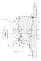
図1は、本発明のテラヘルツ波発生装置の実施形態を示す図である。この図1では、光伝導アンテナについては図2中のS−S線での断面図、光源装置についてはブロック図を示す。図2は、図1に示すテラヘルツ波発生装置の光伝導アンテナの平面図、図3は、図1に示すテラヘルツ波発生装置の光源装置の断面斜視図、図4は、図3中のA−A線での断面図、図5は、図3中のB−B線での断面図である。なお、以下では、図1、図3〜5中の上側を「上」、下側を「下」として説明を行う。
Hereinafter, a photoconductive antenna, a terahertz wave generation device, a camera, an imaging device, and a measurement device according to the present invention will be described in detail based on preferred embodiments shown in the accompanying drawings.
<First Embodiment>
FIG. 1 is a diagram showing an embodiment of a terahertz wave generator according to the present invention. In FIG. 1, the photoconductive antenna is a cross-sectional view taken along line SS in FIG. 2, and the light source device is a block diagram. 2 is a plan view of the photoconductive antenna of the terahertz wave generating device shown in FIG. 1, FIG. 3 is a cross-sectional perspective view of the light source device of the terahertz wave generating device shown in FIG. 1, and FIG. FIG. 5 is a sectional view taken along line B-B in FIG. 3. In the following description, the upper side in FIGS. 1 and 3 to 5 will be described as “upper” and the lower side as “lower”.
図1に示すように、テラヘルツ波発生装置1は、励起光である光パルス(パルス光)を発生する光源装置3と、光源装置3で発生した光パルスが照射されることによりテラヘルツ波を発生する光伝導アンテナ2とを有している。なお、テラヘルツ波とは、周波数が、100GHz以上30THz以下の電磁波、特に、300GHz以上3THz以下の電磁波を言う。
図3〜図5に示すように、光源装置3は、本実施形態では、光パルスを発生する光パルス発生部4と、光パルス発生部4で発生した光パルスに対し、パルス圧縮を行う第1のパルス圧縮部5と、第1のパルス圧縮部5でパルス圧縮がなされた光パルスに対し、パルス圧縮を行う第2のパルス圧縮部7と、光パルスを増幅する増幅部6とを有している。
As shown in FIG. 1, a terahertz wave generator 1 generates a terahertz wave by irradiating a light source device 3 that generates a light pulse (pulse light) that is excitation light and a light pulse generated by the light source device 3. And a photoconductive antenna 2. The terahertz wave means an electromagnetic wave having a frequency of 100 GHz to 30 THz, particularly an electromagnetic wave of 300 GHz to 3 THz.
As shown in FIGS. 3 to 5, in the present embodiment, the light source device 3 includes an optical pulse generator 4 that generates an optical pulse and a first pulse that compresses the optical pulse generated by the optical pulse generator 4. 1
増幅部6は、第1のパルス圧縮部5の前段、または第1のパルス圧縮部5と第2のパルス圧縮部7との間に設けられるが、図示の構成では、増幅部6は、第1のパルス圧縮部5と第2のパルス圧縮部7との間に設けられている。これにより、第1のパルス圧縮部5でパルス圧縮がなされた光パルスが、増幅部6で増幅され、増幅部6で増幅された光パルスが、第2のパルス圧縮部7でパルス圧縮がなされる。
The amplifying
また、光源装置3から出射する光パルスのパルス幅(半値幅)は、特に限定されないが、1f秒以上800f秒以下であることが好ましく、10f秒以上200f秒以下であることよりが好ましい。
また、光源装置3から出射する光パルスの周波数は、後述する光伝導アンテナ2のi型半導体層24のバンドギャップに対応する周波数以上に設定される。
The pulse width (half width) of the light pulse emitted from the light source device 3 is not particularly limited, but is preferably 1 f second or more and 800 f second or less, more preferably 10 f second or more and 200 f second or less.
The frequency of the light pulse emitted from the light source device 3 is set to be equal to or higher than the frequency corresponding to the band gap of the i-
また、光パルス発生部4は、例えば、DBRレーザー、DFBレーザー、モード同期レーザー等、いわゆる半導体レーザーを用いることができる。この光パルス発生部4で発生する光パルスのパルス幅は、特に限定されないが、1p秒以上100p秒以下であることが好ましい。
また、第1のパルス圧縮部5は、可飽和吸収に基づくパルス圧縮を行うものである。すなわち、第1のパルス圧縮部5は、可飽和吸収体を有しており、その可飽和吸収体により、光パルスを圧縮し、そのパルス幅を減少させる。
また、第2のパルス圧縮部7は、群速度分散補償に基づくパルス圧縮を行うものである。すなわち、第2のパルス圧縮部7は、群速度分散補償媒体、本実施形態では、結合導波路構造を有しており、その結合導波路構造により、光パルスを圧縮し、そのパルス幅を減少させる。
The optical pulse generator 4 may be a so-called semiconductor laser such as a DBR laser, a DFB laser, or a mode-locked laser. The pulse width of the optical pulse generated by the optical pulse generator 4 is not particularly limited, but is preferably 1 psec or more and 100 psec or less.
The first
The second
また、光源装置3の光パルス発生部4と、第1のパルス圧縮部5と、増幅部6と、第2のパルス圧縮部7とは、一体化、すなわち同一基板上に集積されている。
具体的には、光源装置3は、半導体基板である基板31と、基板31上に設けられたクラッド層32と、クラッド層32上に設けられた活性層33と、活性層33上に設けられた導波路構成プロセス用エッチングストップ層34と、導波路構成プロセス用エッチングストップ層34上に設けられたクラッド層35と、クラッド層35上に設けられたコンタクト層36と、導波路構成プロセス用エッチングストップ層34上に設けられた絶縁層37と、基板31の表面に設けられたクラッド層32側の電極38と、コンタクト層36および絶縁層37の表面に設けられたクラッド層35側の電極391、392、393、394および395とを有している。また、光パルス発生部4の導波路構成プロセス用エッチングストップ層34と、クラッド層35との間には、回折格子30が設けられている。なお、導波路構成プロセス用エッチングストップ層は、活性層の直上に限らず、例えば、クラッド層の中に設けられていてもよい。
In addition, the light pulse generation unit 4, the first
Specifically, the light source device 3 is provided on a
なお、各部の構成材料は、特に限定されないが、一例として、基板31、コンタクト層36としては、それぞれ、例えば、GaAs等が挙げられる。また、クラッド層32、35、導波路構成プロセス用エッチングストップ層34、回折格子30としては、それぞれ、例えば、AlGaAs等が挙げられる。また、活性層33としては、例えば、多重量子井戸と呼ばれる量子効果を用いた構成等が挙げられる。具体的には、活性層33としては、例えば、井戸層(GaAs井戸層)とバリア層(AlGaAsバリア層)とを交互に複数ずつ設けてなる多重量子井戸等で構成された分布屈折率型多重量子井戸と呼ばれる構造のもの等が挙げられる。
In addition, although the constituent material of each part is not specifically limited, As an example, as the board |
また、図示の構成では、光源装置3における導波路は、クラッド層32と、活性層33と、導波路構成プロセス用エッチングストップ層34と、クラッド層35とで構成されている。また、クラッド層35は、導波路の上部にのみ、その導波路に対応した形状に設けられている。また、クラッド層35は、不要な部分をエッチングにより除去することにより形成されている。なお、製造方法によっては、導波路構成プロセス用エッチングストップ層34を省略してもよい。
In the illustrated configuration, the waveguide in the light source device 3 includes a
また、クラッド層35およびコンタクト層36は、それぞれ、2つずつ設けられている。一方のクラッド層35およびコンタクト層36は、光パルス発生部4と、第1のパルス圧縮部5と、増幅部6と、第2のパルス圧縮部7の一部を構成し、連続的に設けられており、他方のクラッド層35およびコンタクト層36は、第2のパルス圧縮部7の一部を構成している。すなわち、第2のパルス圧縮部7には、1対のクラッド層35と、1対のコンタクト層36とが設けられている。
Two
また、電極391は、光パルス発生部4のクラッド層35に対応するように設けられ、また、電極392は、第1のパルス圧縮部5のクラッド層35に対応するように設けられ、また、電極393は、増幅部6のクラッド層35に対応するように設けられ、また、電極394および395は、それぞれ、第2のパルス圧縮部7の2つのクラッド層35に対応するように設けられている。なお、電極38は、光パルス発生部4、第1のパルス圧縮部5、増幅部6および第2のパルス圧縮部7の共通の電極である。そして、電極38と電極391とで光パルス発生部4の1対の電極が構成され、また、電極38と電極392とで第1のパルス圧縮部5の1対の電極が構成され、また、電極38と電極393とで増幅部6の1対の電極が構成され、また、電極38と電極394、電極38と電極395とで第2のパルス圧縮部7の2対の電極が構成される。
In addition, the
なお、光源装置3の全体形状は、図示の構成では、直方体をなしているが、これに限定されないことは、言うまでもない。
また、光源装置3の寸法は、特に限定されないが、例えば、1mm以上10mm以下×0.5mm以上5mm以下×0.1mm以上1mm以下とすることができる。
なお、本発明では、光源装置の構成は、前述した構成に限定されないことは、言うまでもない。
In addition, although the whole shape of the light source device 3 has comprised the rectangular parallelepiped in the structure of illustration, it cannot be overemphasized that it is not limited to this.
Moreover, although the dimension of the light source device 3 is not specifically limited, For example, it is 1 mm or more and 10 mm or less x0.5 mm or more and 5 mm or less x0.1 mm or more and 1 mm or less.
In the present invention, it goes without saying that the configuration of the light source device is not limited to the configuration described above.
次に、光伝導アンテナ2について説明する。
図1および図2に示すように、光伝導アンテナ2は、基板21と、基板21上に設けられた光伝導アンテナ本体20とを有している。
基板21としては、光伝導アンテナ本体20を支持できるものであれば、特に限定されず、例えば、各種の半導体材料で構成された半導体基板、各種の樹脂材料で構成された樹脂基板、各種のガラス材料で構成されたガラス基板等を用いることができるが、半導体基板が好ましい。また、基板21として半導体基板を用いる場合、その半導体材料としては、特に限定されず、各種のものを用いることができるが、III−V属化合物半導体が好ましい。また、III−V属化合物半導体としては、特に限定されず、例えば、GaAs、InP、InAs、InSb等が挙げられる。
Next, the photoconductive antenna 2 will be described.
As shown in FIGS. 1 and 2, the photoconductive antenna 2 includes a
The
また、基板21の形状は、図示の構成では、後述するn型半導体層22とi型半導体層24とp型半導体層23との積層方向から見たとき、四角形をなしている。なお、基板21の形状は、四角形には限定されず、この他、例えば、円形、楕円形や、三角形、五角形、六角形等の他の多角形等が挙げられる。以下では、「n型半導体層22とi型半導体層24とp型半導体層23との積層方向から見たとき」を、「平面視」とも言う。また、「n型半導体層22とi型半導体層24とp型半導体層23との積層方向」を、単に、「積層方向」とも言う。
In the configuration shown in the drawing, the shape of the
光伝導アンテナ本体20は、n型半導体層(第1導電層)22と、テラヘルツ波を発生するi型半導体層(半導体層)24と、p型半導体層(第2導電層)23と、誘電体層25と、被覆層26と、テラヘルツ波を反射させる反射層(第1反射層)27と、1対の電極を構成する電極28(第1電極)および電極(第2電極)29とを有している。
この場合、基板21上に、n型半導体層22と、i型半導体層24と、p型半導体層23とが、基板21側からこの順序で積層されている(設けられている)。すなわち、基板21上には、n型半導体層と、i型半導体層と、p型半導体層とが基板21側からこの順序で積層された積層体(pin構造)が形成されている。さらに換言すれば、i型半導体層24は、n型半導体層22と、p型半導体層23とに挟まれて形成されている。
The
In this case, the n-
また、電極28は、基板21およびn型半導体層22上に設けられている。すなわち、電極28は、n型半導体層22に接触し、n型半導体層22に電気的に接続されている。
また、電極29は、p型半導体層23および誘電体層25上に設けられている。すなわち、電極29は、p型半導体層23に接触し、p型半導体層23に電気的に接続されている。また、電極29は、積層方向から誘電体層25の基板21と反対側の面に接触しており、テラヘルツ波を反射させる第2反射層を兼ねている。第2反射層を設けることにより、誘電体層25の上面(誘電体層25の基板21と反対側の面)から漏れるテラヘルツ波を誘電体層25内に反射し、テラヘルツ波を効率良く導くことができる。なお、第2反射層を電極29とは別に設けてもよいことは言うまでもない。
The
The
また、電極29は、p型半導体層23に対応する部位に設けられた開口291を有している。開口291により、p型半導体層23のi型半導体層24と反対側の面が露出する。そして、このテラヘルツ波発生装置1では、光源装置3で発生した光パルスは、開口291を介してp型半導体層23に照射されるようになっている。したがって、開口291により、光パルスが通過(透過)窓部が構成される。なお、開口291に、光パルスを透過可能な光透過性を有する図示しない保護層が設けられていてもよい。
Further, the
また、開口291の形状は、図示の構成では、平面視で、円形をなしている。なお、開口291形状は、円形には限定されず、この他、例えば、楕円形や、三角形、四角形、五角形、六角形等の多角形等が挙げられる。
また、平面視での開口291の面積Sは、特に限定されず、諸条件に応じて適宜設定されるものであるが、1μm2以上10000μm2以下であることが好ましく、10μm2以上100μm2以下であることがより好ましい。
開口291の面積Sが、前記下限値未満であると、他の条件によってはその開口291の部位のみに光パルスを集光させることができず、光パルスが無駄になり、また、前記上限値を超えると、他の条件によってはi型半導体層24内の複数の領域において発生したテラヘルツ波同士が干渉してしまう。
Further, the shape of the
Further, the area S of the
If the area S of the
また、誘電体層25は、基板21上に設けられている。この誘電体層25は、積層体の側面におけるi型半導体層24の部分、すなわち、積層方向に対して垂直な法線を有するi型半導体層24の表面に接触している。なお、積層体の側面は、i型半導体層24のn型半導体層22とp型半導体層23との間において露出する面、あるいは、n型半導体層22およびp型半導体層23に接触しない面とも言える。
The
また、被覆層26は、基板21およびn型半導体層22上に設けられている。この被覆層26は、積層体の側面におけるi型半導体層24の部分のうち、誘電体層25が接触していない部位に接触している(覆っている)。これにより、積層体の側面におけるi型半導体層24の部分は、誘電体層25および被覆層26により覆われている。これによって、i型半導体層24の腐食等を防止することができる。
The
また、反射層27は、基板21上に設けられ、積層方向から誘電体層25の基板21側の面に接触している。すなわち、反射層27は、基板21と誘電体層25との間に介在している。換言すれば、誘電体層25は、反射層27と前述の第2反射層である電極29とによって積層方向から挟まれている。この反射層27を設けることにより、誘電体層25の下面から基板21側に漏れてしまうテラヘルツ波を誘電体層25内に反射することができ、これによりテラヘルツ波を効率良く導くことができる。なお、前記電極28で反射層27を構成し、電極28が第1反射層を兼ねるようにしてもよいことは言うまでもない。
The
また、反射層27の厚さdは、特に限定されず、諸条件に応じて適宜設定されるものであるが、10mm以上500mm以下であることが好ましく、30mm以上300mm以下であることがより好ましい。
反射層27の厚さdが、前記下限値未満であると、他の条件によってはテラヘルツ波が反射層27に吸収されてしまい、また、前記上限値を超えると、他の条件によってはその反射層27が邪魔になる。
Further, the thickness d of the
If the thickness d of the
前記n型半導体層22は、n型(第1導電型)の不純物を含む半導体材料で構成されている。n型半導体層22のキャリア濃度(不純物濃度)は、1×10¹⁷/cm3以上であることが好ましく、1×1020/cm3以上であることがより好ましく、1×1020/cm3以上1×1025/cm3以下であることがさらに好ましい。なお、n型不純物としては、特に限定されず、例えば、Si、Ge、S、Se等が挙げられる。
また、n型半導体層22の厚さd1は、特に限定されず、諸条件に応じて適宜設定されるものであるが、1μm以上4mm以下であることが好ましく、1μm以上10μm以下であることがより好ましい。
The n-
Further, the thickness d1 of the n-
また、p型半導体層23は、p型(第2導電型)の不純物を含む半導体材料で構成されている。p型半導体層23のキャリア濃度は、1×10¹⁷/cm3以上であることが好ましく、1×1020/cm3以上であることがより好ましく、1×1020/cm3以上1×1025/cm3以下であることがさらに好ましい。なお、p型不純物としては、特に限定されず、例えば、Zn、Mg、C等が挙げられる。
The p-
また、p型半導体層23は、平面視で、電極29の開口291内に位置し、p型半導体層23の開口291の外側に位置する部位よりも厚さが薄い薄肉部231を有している。これにより、光パルスがp型半導体層23で吸収されてしまうことを抑制することができ、また、p型半導体層23の開口291の外側に位置する部位の厚さを適正値に設定することができる。
また、p型半導体層23の薄肉部231の厚さd2は、特に限定されず、諸条件に応じて適宜設定されるものであるが、1μm以上2mm以下であることが好ましく、1μm以上10μm以下であることがより好ましい。
Further, the p-
Further, the thickness d2 of the
また、i型半導体層24は、半導体材料で構成されている。このi型半導体層24を構成する半導体材料は、真性半導体であることが好ましいが、n型不純物やp型不純物を少量含んでいてもよい。
換言すると、i型半導体層24は、n型不純物を含む場合は、n型半導体層22よりもキャリア濃度が低いといえ、また、p型不純物を含む場合は、p型半導体層23よりもキャリア濃度が低いといえる。なお、i型半導体層24は、n型不純物、p型不純物のいずれを含む場合でもn型半導体層22およびp型半導体層23よりもキャリア濃度が低いことが好ましい。
具体的には、i型半導体層24のキャリア濃度は、1×10¹⁸/cm3以下であることが好ましく、1×1012/cm3以上1×1018/cm3以下であることがより好ましく、1×1012/cm3以上1×1016/cm3以下であることがさらに好ましい。
The i-
In other words, when the i-
Specifically, the carrier concentration of the i-
また、i型半導体層24の厚さd3は、特に限定されず、諸条件に応じて適宜設定されるものであるが、1μm以上4mm以下であることが好ましく、1μm以上10μm以下であることがより好ましい。
i型半導体層24の厚さd3が、前記下限値未満であると、他の条件によってはi型半導体層24の形成が困難であり、また、前記上限値を超えると、他の条件によっては耐電圧が不十分となり、i型半導体層24内に大きい電界強度の電界を形成できず、これにより高い強度のテラヘルツ波を発生することができない。
なお、p型半導体層23、n型半導体層22、i型半導体層24の半導体材料としては、それぞれ、特に限定されず、各種のものを用いることができるが、III−V属化合物半導体が好ましい。また、III−V属化合物半導体としては、特に限定されず、例えば、GaAs、InP、InAs、InSb等が挙げられる。
In addition, the thickness d3 of the i-
If the thickness d3 of the i-
The semiconductor materials of the p-
また、誘電体層25は、誘電体材料で構成され、i型半導体層24で発生したテラヘルツ波を所定方向に導く機能を有している。この誘電体層25を構成する誘電体材料の比誘電率(誘電率)は、i型半導体層24を構成する半導体材料の比誘電率よりも高いことが好ましい。テラヘルツ波は、誘電率のより高い物質中を進もうとする性質を有している。したがって、i型半導体層24で発生したテラヘルツ波は、そのi型半導体層24の側面から誘電体層25に入射し、その誘電体層25内を進む。このようにしてi型半導体層24で発生したテラヘルツ波が誘電体層25により所定の方向に導かれ、これによって、指向性を有し、高い強度のテラヘルツ波を発生することができる。
The
また、誘電体層25の形状は、特に限定されないが、図示の構成では、平面視で、扇形の中心側の部分(扇形の外形を構成する2つの直線の交点を含む部分)を除いたような形状をなしており、誘電体層25のテラヘルツ波を出射する出射部251の形状が、平面視で、円弧状をなしている。すなわち、平面視で、誘電体層25の幅Wは、i型半導体層24に対して近位側から遠位側に向って(i型半導体層24から離れるに従って)漸増している。これにより、誘電体層25によりテラヘルツ波を効率良く導くことができる。
なお、誘電体層25は、その一部のみが幅Wがi型半導体層24に対して近位側から遠位側に向って漸増してもよい。すなわち、誘電体層25は、平面視で、幅Wがi型半導体層24に対して近位側から遠位側に向って漸増する部位を有していればよい。
In addition, the shape of the
Only a part of the
また、誘電体層25を構成する誘電体材料の比誘電率は、20以上であることが好ましく、30以上200以下であることがより好ましい。
このような誘電体材料(高誘電率材料)としては、例えば、窒素添加ハフニウムアルミネート(比誘電率:20)、酸化ハフニウム(比誘電率:23)、酸化イットリウム(比誘電率:25)、酸化ランタン(比誘電率:27)、五酸化ニオブ(比誘電率:41)、二酸化チタン(ルチル)(比誘電率:80)、酸化チタン(比誘電率:160)等が挙げられる。
The relative dielectric constant of the dielectric material constituting the
As such a dielectric material (high dielectric constant material), for example, nitrogen-added hafnium aluminate (relative permittivity: 20), hafnium oxide (relative permittivity: 23), yttrium oxide (relative permittivity: 25), Examples thereof include lanthanum oxide (relative permittivity: 27), niobium pentoxide (relative permittivity: 41), titanium dioxide (rutile) (relative permittivity: 80), and titanium oxide (relative permittivity: 160).
また、被覆層26の構成材料の比誘電率は、誘電体層25を構成する誘電体材料の比誘電率よりも低いことが好ましく、i型半導体層24を構成する半導体材料の比誘電率よりも低いことがより好ましい。これにより、誘電体層25によりテラヘルツ波を効率良く導くことができる。
また、被覆層26の構成材料の比誘電率は、20以下であることが好ましく、2以上10以下であることがより好ましい。
The relative dielectric constant of the constituent material of the
Moreover, the relative dielectric constant of the constituent material of the
このような被覆層26の構成材料(低誘電率材料)としては、例えば、ポリイミド(比誘電率:3)、ボラジン系化合物(比誘電率:2.3)、SiN(比誘電率:7)、SiO2(比誘電率:4)、水酸化シロキサン(比誘電率:3)、ベンゾシクロブテン(比誘電率:2.7)、フッ素系樹脂(比誘電率:2.7)等が挙げられる。
なお、電極28および29には、それぞれ、図示しないパッド、導線、コネクター等を介して電源装置18が電気的に接続され、電極28と電極29との間に、電極28側が正となるように、直流電圧が印加される。
Such constituent material of the coating layer 26 (low-k material), for example, polyimide (relative dielectric constant: 3), Bo Rajin compound (dielectric constant: 2.3), SiN (dielectric constant: 7 ), SiO 2 (relative dielectric constant: 4), water oxidation Shi Rokisan (relative dielectric constant: 3), benzocyclobutene (dielectric constant: 2.7), fluorine-based resin (dielectric constant: 2.7) Etc.
The
次に、テラヘルツ波発生装置1の作用について説明する。
テラヘルツ波発生装置1では、まず、光源装置3の光パルス発生部4で、光パルスを発生する。光パルス発生部4で発生した光パルスのパルス幅は、目標のパルス幅に比べて大きい。その光パルス発生部4で発生した光パルスは、導波路を通り、第1のパルス圧縮部5、増幅部6、第2のパルス圧縮部7をこの順序で順次通過する。
Next, the operation of the terahertz wave generator 1 will be described.
In the terahertz wave generator 1, first, an optical pulse is generated by the optical pulse generator 4 of the light source device 3. The pulse width of the optical pulse generated by the optical pulse generator 4 is larger than the target pulse width. The optical pulse generated by the optical pulse generation unit 4 passes through the waveguide, and sequentially passes through the first
まず、第1のパルス圧縮部5で、光パルスに対し、可飽和吸収に基づくパルス圧縮がなされ、光パルスのパルス幅が減少する。次に、増幅部6で、光パルスが増幅される。最後に、第2のパルス圧縮部7で、光パルスに対し、群速度分散補償に基づくパルス圧縮がなされ、光パルスのパルス幅がさらに減少する。このようにして、目標のパルス幅の光パルスが発生し、第2のパルス圧縮部7から出射する。
First, in the first
光源装置3から出射した光パルスは、光伝導アンテナ2の電極29の開口291に照射され、i型半導体層24でテラヘルツ波が発生する。このテラヘルツ波は、i型半導体層24の側面から誘電体層25に入射し、その誘電体層25内を進み、誘電体層25により所定の方向に導かれる。また、誘電体層25内を進むテラヘルツ波は、電極29および反射層27で反射し、誘電体層25の上面または下面(積層方向の面)から漏れてしまうことが防止され、これによりテラヘルツ波を効率良く導くことができる。
The light pulse emitted from the light source device 3 is applied to the
以上説明したように、このテラヘルツ波発生装置1によれば、i型半導体層24で発生したテラヘルツ波が誘電体層25により所定の方向に導かれ、これによって、指向性を有する。この結果、高い強度のテラヘルツ波を発生することができる。
また、光源装置3が第1のパルス圧縮部5、増幅部6および第2のパルス圧縮部7を有しているので、光源装置3の小型化、ひいてはテラヘルツ波発生装置1の小型化を図りつつ、所望の波高で、かつ所望のパルス幅の光パルスを発生することができ、これにより、所望のテラヘルツ波を確実に発生することができる。
As described above, according to the terahertz wave generating device 1, the terahertz wave generated in the i-
In addition, since the light source device 3 includes the first
<イメージング装置の実施形態>
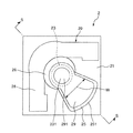
図6は、本発明のイメージング装置の実施形態を示すブロック図、図7は、図6に示すイメージング装置のテラヘルツ波検出部を示す平面図、図8は、対象物のテラヘルツ帯でのスペクトルを示すグラフ、図9は、対象物の物質A、BおよびCの分布を示す画像の図である。
<Embodiment of Imaging Apparatus>
6 is a block diagram showing an embodiment of the imaging apparatus of the present invention, FIG. 7 is a plan view showing a terahertz wave detection unit of the imaging apparatus shown in FIG. 6, and FIG. 8 is a spectrum of the target in the terahertz band. The graph shown in FIG. 9 is an image showing the distribution of the substances A, B and C of the object.
図6に示すように、イメージング装置100は、テラヘルツ波を発生するテラヘルツ波発生部9と、テラヘルツ波発生部9から出射し、対象物150を透過または反射したテラヘルツ波を検出するテラヘルツ波検出部11と、テラヘルツ波検出部11の検出結果に基づいて、対象物150の画像、すなわち、画像データを生成する画像形成部12とを備えている。なお、テラヘルツ波発生部9の構成は、前記テラヘルツ波発生装置1と同様であるので、テラヘルツ波発生部9についての説明は省略する。
As illustrated in FIG. 6, the
また、テラヘルツ波検出部11としては、目的の波長のテラヘルツ波を通過させるフィルター15と、フィルター15を通過した前記目的の波長のテラヘルツ波を検出する検出部17とを備えたものを用いる。また、検出部17としては、テラヘルツ波を熱に変換して検出するもの、すなわち、テラヘルツ波を熱に変換し、そのテラヘルツ波のエネルギー(強度)を検出し得るものを用いる。このような検出部としては、例えば、焦電センサー、ボロメーター等が挙げられる。なお、テラヘルツ波検出部11としては、前記の構成のものに限定されないことは、言うまでもない。
The terahertz
また、フィルター15は、2次元的に配置された複数の画素(単位フィルター部)16を有している。すなわち、各画素16は、行列状に配置されている。
また、各画素16は、互いに異なる波長のテラヘルツ波を通過させる複数の領域、すなわち、通過させるテラヘルツ波の波長(以下、「通過波長」とも言う)が互いに異なる複数の領域を有している。なお、図示の構成では、各画素16は、第1の領域161、第2の領域162、第3の領域163および第4の領域164を有している。
The
Each
また、検出部17は、フィルター15の各画素16の第1の領域161、第2の領域162、第3の領域163および第4の領域164に対応してそれぞれ設けられた第1の単位検出部171、第2の単位検出部172、第3の単位検出部173および第4の単位検出部174を有している。各第1の単位検出部171、各第2の単位検出部172、各第3の単位検出部173および各第4の単位検出部174は、それぞれ、各画素16の第1の領域161、第2の領域162、第3の領域163および第4の領域164を通過したテラヘルツ波を熱に変換して検出する。これにより、各画素16のそれぞれにおいて、4つの目的の波長のテラヘルツ波をそれぞれ確実に検出することができる。
The
次に、イメージング装置100の使用例について説明する。
まず、分光イメージングの対象となる対象物150が、3つの物質A、BおよびCで構成されているとする。イメージング装置100は、この対象物150の分光イメージングを行う。また、ここでは、一例として、テラヘルツ波検出部11は、対象物150を反射したテラヘルツ波を検出することとする。
Next, a usage example of the
First, it is assumed that an
テラヘルツ波検出部11のフィルター15の各画素16においては、第1の領域161および第2の領域162を使用する。
また、第1の領域161の通過波長をλ1、第2の領域162の通過波長をλ2とし、対象物150で反射したテラヘルツ波の波長λ1の成分の強度をα1、波長λ2の成分の強度をα2としたとき、その強度α2と強度α1の差分(α2−α1)が、物質Aと物質Bと物質Cとで、互いに顕著に区別できるように、前記第1の領域161の通過波長λ1および第2の領域162の通過波長λ2が設定されている。
In each
Further, the transmission wavelength of the
図8に示すように、物質Aにおいては、対象物150で反射したテラヘルツ波の波長λ2の成分の強度α2と波長λ1の成分の強度α1の差分(α2−α1)は、正値となる。
また、物質Bにおいては、強度α2と強度α1の差分(α2−α1)は、零となる。
また、物質Cにおいては、強度α2と強度α1の差分(α2−α1)は、負値となる。
イメージング装置100により、対象物150の分光イメージングを行う際は、まず、テラヘルツ波発生部9により、テラヘルツ波を発生し、そのテラヘルツ波を対象物150に照射する。そして、対象物150で反射したテラヘルツ波をテラヘルツ波検出部11で、α1およびα2として検出する。この検出結果は、画像形成部12に送出される。なお、この対象物150へのテラヘルツ波の照射および対象物150で反射したテラヘルツ波の検出は、対象物150の全体に対して行う。
As shown in FIG. 8, in the substance A, the difference (α2−α1) between the intensity α2 of the component of wavelength λ2 and the intensity α1 of the component of wavelength λ1 reflected by the
In the substance B, the difference (α2−α1) between the intensity α2 and the intensity α1 is zero.
Further, in the substance C, the difference (α2−α1) between the intensity α2 and the intensity α1 is a negative value.
When spectral imaging of the
画像形成部12においては、前記検出結果に基づいて、フィルター15の第2の領域162を通過したテラヘルツ波の波長λ2の成分の強度α2と、第1の領域161を通過したテラヘルツ波の波長λ1の成分の強度α1の差分(α2−α1)を求める。そして、対象物150のうち、前記差分が正値となる部位を物質A、前記差分が零となる部位を物質B、前記差分が負値となる部位を物質Cと判断し、特定する。
In the
また、画像形成部12では、図9に示すように、対象物150の物質A、BおよびCの分布を示す画像の画像データを作成する。この画像データは、画像形成部12から図示しないモニターに送出され、そのモニターにおいて、対象物150の物質A、BおよびCの分布を示す画像が表示される。この場合、例えば、対象物150の物質Aの分布する領域は黒色、物質Bの分布する領域は灰色、物質Cの分布する領域は白色に色分けして表示される。このイメージング装置100では、以上のように、対象物150を構成する各物質の同定と、その各物質の分布測定とを同時に行うことができる。
なお、イメージング装置100の用途は、前記のものに限らず、例えば、人物に対してテラヘルツ波を照射し、その人物を透過または反射したテラヘルツ波を検出し、画像形成部12において処理を行うことにより、その人物が、拳銃、ナイフ、違法な薬物等を所持しているか否かを判別することもできる。
In addition, the
The application of the
<計測装置の実施形態>
図10は、本発明の計測装置の実施形態を示すブロック図である。
以下、計測装置の実施形態について、前述したイメージング装置の実施形態との相違点を中心に説明し、同様の事項については前述の実施形態と同じ符号を付し、その詳細な説明を省略する。
図10に示すように、計測装置200は、テラヘルツ波を発生するテラヘルツ波発生部9と、テラヘルツ波発生部9から出射し、対象物160を透過または反射したテラヘルツ波を検出するテラヘルツ波検出部11と、テラヘルツ波検出部11の検出結果に基づいて、対象物160を計測する計測部13とを備えている。
<Embodiment of measuring device>
FIG. 10 is a block diagram showing an embodiment of the measuring apparatus of the present invention.
Hereinafter, the embodiment of the measurement apparatus will be described with a focus on the differences from the above-described embodiment of the imaging apparatus, the same matters are denoted by the same reference numerals as those of the above-described embodiment, and the detailed description thereof will be omitted.
As illustrated in FIG. 10, the
次に、計測装置200の使用例について説明する。
計測装置200により、対象物160の分光計測を行う際は、まず、テラヘルツ波発生部9により、テラヘルツ波を発生し、そのテラヘルツ波を対象物160に照射する。そして、対象物160を透過または反射したテラヘルツ波をテラヘルツ波検出部11で検出する。この検出結果は、計測部13に送出される。なお、この対象物160へのテラヘルツ波の照射および対象物160を透過または反射したテラヘルツ波の検出は、対象物160の全体に対して行う。
計測部13においては、前記検出結果から、フィルター15の第1の領域161、第2の領域162、第3の領域163および第4の領域164を通過したテラヘルツ波のそれぞれの強度を把握し、対象物160の成分およびその分布の分析等を行う。
Next, a usage example of the measuring
When performing spectroscopic measurement of the
In the
<カメラの実施形態>
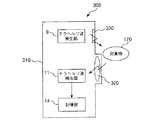
図11は、本発明のカメラの実施形態を示すブロック図である。また、図12に本発明のカメラの実施形態を示す概略斜視図を示す。
以下、カメラの実施形態について、前述したイメージング装置の実施形態との相違点を中心に説明し、同様の事項については前述の実施形態と同じ符号を付し、その詳細な説明を省略する。
<Embodiment of Camera>
FIG. 11 is a block diagram showing an embodiment of the camera of the present invention. FIG. 12 is a schematic perspective view showing an embodiment of the camera of the present invention.
Hereinafter, the embodiment of the camera will be described focusing on the differences from the above-described embodiment of the imaging apparatus, the same matters will be denoted by the same reference numerals as those of the above-described embodiment, and detailed description thereof will be omitted.
図11および図12に示すように、カメラ300は、テラヘルツ波を発生するテラヘルツ波発生部9と、テラヘルツ波発生部9から出射し、対象物170にて反射したテラヘルツ波を検出するテラヘルツ波検出部11と、記憶部14とを備えている。そして、これらの各部はカメラ300の筐体310に収められている。また、カメラ300は、対象物170にて反射したテラヘルツ波をテラヘルツ波検出部11に収束(結像)させるレンズ(光学系)320と、テラヘルツ波発生部9にて発生したテラヘルツ波を筐体310の外部へ出射させるための窓部330を備える。レンズ320や窓部330はテラヘルツ波を透過・屈折させるシリコン、石英、ポリエチレンなどの部材によって構成されている。なお、窓部330は、スリットのように単に開口が設けられている構成としても良い。
As shown in FIGS. 11 and 12, the
次に、カメラ300の使用例について説明する。
カメラ300により、対象物170を撮像する際は、まず、テラヘルツ波発生部9により、テラヘルツ波を発生し、そのテラヘルツ波を対象物170に照射する。そして、対象物170にて反射したテラヘルツ波をレンズ320によってテラヘルツ波検出部11に収束(結像)させて検出する。この検出結果は、記憶部14に送出され、記憶される。なお、この対象物170へのテラヘルツ波の照射および対象物170にて反射したテラヘルツ波の検出は、対象物170の全体に対して行う。また、前記検出結果は、例えば、パーソナルコンピューター等の外部装置に送信することもできる。パーソナルコンピューターでは、前記検出結果に基づいて、各処理を行うことができる。
Next, a usage example of the
When the
以上、本発明の光伝導アンテナ、テラヘルツ波発生装置、カメラ、イメージング装置および計測装置を、図示の実施形態に基づいて説明したが、本発明はこれに限定されるものではなく、各部の構成は、同様の機能を有する任意の構成のものに置換することができる。また、本発明に、他の任意の構成物が付加されていてもよい。
また、前記実施形態では、第1導電層をn型半導体層とし、第2導電層をp型半導体層としたが、本発明では、これに限定されず、第1導電層をp型半導体層とし、第2導電層をn型半導体層としてもよい。
また、本発明では、光源装置において、光パルス発生部が別体になっていてもよい。
As described above, the photoconductive antenna, the terahertz wave generation device, the camera, the imaging device, and the measurement device of the present invention have been described based on the illustrated embodiment, but the present invention is not limited to this, and the configuration of each part is It can be replaced with any configuration having a similar function. In addition, any other component may be added to the present invention.
In the embodiment, the first conductive layer is an n-type semiconductor layer and the second conductive layer is a p-type semiconductor layer. However, the present invention is not limited to this, and the first conductive layer is a p-type semiconductor layer. The second conductive layer may be an n-type semiconductor layer.
In the present invention, in the light source device, the light pulse generator may be a separate body.
1…テラヘルツ波発生装置 2…光伝導アンテナ 20…光伝導アンテナ本体 21…基板 22…n型半導体層 23…p型半導体層 231…薄肉部 24…i型半導体層 25…誘電体層 251…出射部 26…被覆層 27…反射層 28、29…電極 291…開口 3…光源装置 30…回折格子 31…基板 32、35…クラッド層 33…活性層 34…導波路構成プロセス用エッチングストップ層 36…コンタクト層 37…絶縁層 38、391〜395…電極 4…光パルス発生部 5…第1のパルス圧縮部 6…増幅部 7…第2のパルス圧縮部 9…テラヘルツ波発生部 11…テラヘルツ波検出部 12…画像形成部 13…計測部 14…記憶部 15…フィルター 16…画素 161…第1の領域 162…第2の領域 163…第3の領域 164…第4の領域 17…検出部 171…第1の単位検出部 172…第2の単位検出部 173…第3の単位検出部 174…第4の単位検出部 18…電源装置 100…イメージング装置 150、160、170…対象物 200…計測装置 300…カメラ 310…筐体 320…レンズ 330…窓部
DESCRIPTION OF SYMBOLS 1 ... Terahertz wave generator 2 ...
Claims (17)
第1導電型の不純物を含む半導体材料で構成された第1導電層と、
前記第1導電型と異なる第2導電型の不純物を含む半導体材料で構成された第2導電層と、
前記第1導電層と前記第2導電層との間に挟まれ、かつ前記第1導電層の半導体材料または前記第2導電層の半導体材料よりもキャリア濃度が低い半導体材料で構成された半導体層と、
前記第1導電層に電気的に接続する第1電極と、
前記第2導電層に電気的に接続され、かつパルス光が通過する開口を有する第2電極と、
前記第1導電層と前記半導体層と前記第2導電層との積層方向に垂直な法線を有する前記半導体層の面に接触し、誘電体材料で構成された誘電体層と、
前記積層方向に垂直な法線を有する前記半導体層の面のうち、前記誘電体層が接触していない部位を覆う被覆層と、を備えることを特徴とする光伝導アンテナ。 A photoconductive antenna that generates terahertz waves,
A first conductive layer made of a semiconductor material containing an impurity of the first conductivity type;
A second conductive layer made of a semiconductor material containing an impurity of a second conductivity type different from the first conductivity type;
A semiconductor layer sandwiched between the first conductive layer and the second conductive layer and made of a semiconductor material having a lower carrier concentration than the semiconductor material of the first conductive layer or the semiconductor material of the second conductive layer When,
A first electrode electrically connected to the first conductive layer;
A second electrode electrically connected to the second conductive layer and having an opening through which pulsed light passes;
A dielectric layer made of a dielectric material in contact with a surface of the semiconductor layer having a normal line perpendicular to a stacking direction of the first conductive layer, the semiconductor layer, and the second conductive layer;
A photoconductive antenna , comprising: a covering layer that covers a portion of the surface of the semiconductor layer having a normal line perpendicular to the stacking direction that is not in contact with the dielectric layer .
第1導電型の不純物を含む半導体材料で構成された第1導電層と、
前記第1導電型と異なる第2導電型の不純物を含む半導体材料で構成された第2導電層と、
前記第1導電層と前記第2導電層との間に挟まれ、かつ前記第1導電層の半導体材料または前記第2導電層の半導体材料よりもキャリア濃度が低い半導体材料で構成された半導体層と、
前記第1導電層に電気的に接続する第1電極と、
前記第2導電層に電気的に接続され、かつパルス光が通過する開口を有する第2電極と、
前記第1導電層と前記半導体層と前記第2導電層との積層方向に垂直な法線を有する前記半導体層の面に接触し、誘電体材料で構成された誘電体層と、を備え、
前記第2導電層は、薄肉部を有し、
前記薄肉部は、前記積層方向から見たとき、前記開口内に位置し、前記第2導電層の前記開口の外側に位置する部位よりも厚さが薄い、ことを特徴とする光伝導アンテナ。 A photoconductive antenna that generates terahertz waves,
A first conductive layer made of a semiconductor material containing an impurity of the first conductivity type;
A second conductive layer made of a semiconductor material containing an impurity of a second conductivity type different from the first conductivity type;
A semiconductor layer sandwiched between the first conductive layer and the second conductive layer and made of a semiconductor material having a lower carrier concentration than the semiconductor material of the first conductive layer or the semiconductor material of the second conductive layer When,
A first electrode electrically connected to the first conductive layer;
A second electrode electrically connected to the second conductive layer and having an opening through which pulsed light passes;
A dielectric layer made of a dielectric material in contact with a surface of the semiconductor layer having a normal line perpendicular to a stacking direction of the first conductive layer, the semiconductor layer, and the second conductive layer ;
The second conductive layer has a thin portion,
The thin-walled portion is located in the opening when viewed from the stacking direction, and is thinner than a portion located outside the opening of the second conductive layer .
前記光源にて発生したパルス光が照射されることによりテラヘルツ波を発生する光伝導アンテナと、を備え、
前記光伝導アンテナは、第1導電型の不純物を含む半導体材料で構成された第1導電層と、
前記第1導電型と異なる第2導電型の不純物を含む半導体材料で構成された第2導電層と、
前記第1導電層と前記第2導電層との間に挟まれ、かつ前記第1導電層の半導体材料または前記第2導電層の半導体材料よりもキャリア濃度が低い半導体材料で構成された半導体層と、
前記第1導電層に電気的に接続する第1電極と、
前記第2導電層に電気的に接続され、かつ前記パルス光が通過する開口を有する第2電極と、
前記第1導電層と前記半導体層と前記第2導電層との積層方向に垂直な法線を有する前記半導体層の面に接触し、誘電体材料で構成された誘電体層と、
前記積層方向に垂直な法線を有する前記半導体層の面のうち、前記誘電体層が接触していない部位を覆う被覆層と、を備えることを特徴とするテラヘルツ波発生装置。 A light source that generates pulsed light;
A photoconductive antenna that generates terahertz waves when irradiated with pulsed light generated by the light source,
The photoconductive antenna includes a first conductive layer made of a semiconductor material containing impurities of a first conductivity type,
A second conductive layer made of a semiconductor material containing an impurity of a second conductivity type different from the first conductivity type;
A semiconductor layer sandwiched between the first conductive layer and the second conductive layer and made of a semiconductor material having a lower carrier concentration than the semiconductor material of the first conductive layer or the semiconductor material of the second conductive layer When,
A first electrode electrically connected to the first conductive layer;
A second electrode electrically connected to the second conductive layer and having an opening through which the pulsed light passes;
A dielectric layer made of a dielectric material in contact with a surface of the semiconductor layer having a normal line perpendicular to a stacking direction of the first conductive layer, the semiconductor layer, and the second conductive layer;
A terahertz wave generator comprising: a covering layer that covers a portion of the surface of the semiconductor layer that has a normal line perpendicular to the stacking direction and is not in contact with the dielectric layer .
前記光源にて発生したパルス光が照射されることによりテラヘルツ波を発生する光伝導アンテナと、を備え、
前記光伝導アンテナは、第1導電型の不純物を含む半導体材料で構成された第1導電層と、
前記第1導電型と異なる第2導電型の不純物を含む半導体材料で構成された第2導電層と、
前記第1導電層と前記第2導電層との間に挟まれ、かつ前記第1導電層の半導体材料または前記第2導電層の半導体材料よりもキャリア濃度が低い半導体材料で構成された半導体層と、
前記第1導電層に電気的に接続する第1電極と、
前記第2導電層に電気的に接続され、かつ前記パルス光が通過する開口を有する第2電極と、
前記第1導電層と前記半導体層と前記第2導電層との積層方向に垂直な法線を有する前記半導体層の面に接触し、誘電体材料で構成された誘電体層と、を備え、
前記第2導電層は、薄肉部を有し、
前記薄肉部は、前記積層方向から見たとき、前記開口内に位置し、前記第2導電層の前記開口の外側に位置する部位よりも厚さが薄い、ことを特徴とするテラヘルツ波発生装置。 A light source that generates pulsed light;
A photoconductive antenna that generates terahertz waves when irradiated with pulsed light generated by the light source,
The photoconductive antenna includes a first conductive layer made of a semiconductor material containing impurities of a first conductivity type,
A second conductive layer made of a semiconductor material containing an impurity of a second conductivity type different from the first conductivity type;
A semiconductor layer sandwiched between the first conductive layer and the second conductive layer and made of a semiconductor material having a lower carrier concentration than the semiconductor material of the first conductive layer or the semiconductor material of the second conductive layer When,
A first electrode electrically connected to the first conductive layer;
A second electrode electrically connected to the second conductive layer and having an opening through which the pulsed light passes;
A dielectric layer made of a dielectric material in contact with a surface of the semiconductor layer having a normal line perpendicular to a stacking direction of the first conductive layer, the semiconductor layer, and the second conductive layer ;
The second conductive layer has a thin portion,
The terahertz wave generating device characterized in that the thin-walled portion is located in the opening when viewed from the stacking direction and is thinner than a portion located outside the opening of the second conductive layer. .
前記テラヘルツ波発生部から出射し、対象物を反射したテラヘルツ波を検出するテラヘルツ波検出部と、を備え、
前記テラヘルツ波発生部は、パルス光を発生する光源と、
前記光源にて発生したパルス光が照射されることによりテラヘルツ波を発生する光伝導アンテナと、を備え、
前記光伝導アンテナは、第1導電型の不純物を含む半導体材料で構成された第1導電層と、
前記第1導電型と異なる第2導電型の不純物を含む半導体材料で構成された第2導電層と、
前記第1導電層と前記第2導電層との間に挟まれ、かつ前記第1導電層の半導体材料または前記第2導電層の半導体材料よりもキャリア濃度が低い半導体材料で構成された半導体層と、
前記第1導電層に電気的に接続する第1電極と、
前記第2導電層に電気的に接続され、かつ前記パルス光が通過する開口を有する第2電極と、
前記第1導電層と前記半導体層と前記第2導電層との積層方向に垂直な法線を有する前記半導体層の面に接触し、誘電体材料で構成された誘電体層と、
前記積層方向に垂直な法線を有する前記半導体層の面のうち、前記誘電体層が接触していない部位を覆う被覆層と、を備えることを特徴とするカメラ。 A terahertz wave generator for generating terahertz waves;
A terahertz wave detection unit that detects a terahertz wave that is emitted from the terahertz wave generation unit and reflected from an object; and
The terahertz wave generator includes a light source that generates pulsed light,
A photoconductive antenna that generates terahertz waves when irradiated with pulsed light generated by the light source,
The photoconductive antenna includes a first conductive layer made of a semiconductor material containing impurities of a first conductivity type,
A second conductive layer made of a semiconductor material containing an impurity of a second conductivity type different from the first conductivity type;
A semiconductor layer sandwiched between the first conductive layer and the second conductive layer and made of a semiconductor material having a lower carrier concentration than the semiconductor material of the first conductive layer or the semiconductor material of the second conductive layer When,
A first electrode electrically connected to the first conductive layer;
A second electrode electrically connected to the second conductive layer and having an opening through which the pulsed light passes;
A dielectric layer made of a dielectric material in contact with a surface of the semiconductor layer having a normal line perpendicular to a stacking direction of the first conductive layer, the semiconductor layer, and the second conductive layer;
A camera comprising: a covering layer that covers a portion of the surface of the semiconductor layer having a normal line perpendicular to the stacking direction that is not in contact with the dielectric layer .
前記テラヘルツ波発生部から出射し、対象物を反射したテラヘルツ波を検出するテラヘルツ波検出部と、を備え、
前記テラヘルツ波発生部は、パルス光を発生する光源と、
前記光源にて発生したパルス光が照射されることによりテラヘルツ波を発生する光伝導アンテナと、を備え、
前記光伝導アンテナは、第1導電型の不純物を含む半導体材料で構成された第1導電層と、
前記第1導電型と異なる第2導電型の不純物を含む半導体材料で構成された第2導電層と、
前記第1導電層と前記第2導電層との間に挟まれ、かつ前記第1導電層の半導体材料または前記第2導電層の半導体材料よりもキャリア濃度が低い半導体材料で構成された半導体層と、
前記第1導電層に電気的に接続する第1電極と、
前記第2導電層に電気的に接続され、かつ前記パルス光が通過する開口を有する第2電極と、
前記第1導電層と前記半導体層と前記第2導電層との積層方向に垂直な法線を有する前記半導体層の面に接触し、誘電体材料で構成された誘電体層と、を備え、
前記第2導電層は、薄肉部を有し、
前記薄肉部は、前記積層方向から見たとき、前記開口内に位置し、前記第2導電層の前記開口の外側に位置する部位よりも厚さが薄い、ことを特徴とするカメラ。 A terahertz wave generator for generating terahertz waves;
A terahertz wave detection unit that detects a terahertz wave that is emitted from the terahertz wave generation unit and reflected from an object; and
The terahertz wave generator includes a light source that generates pulsed light,
A photoconductive antenna that generates terahertz waves when irradiated with pulsed light generated by the light source,
The photoconductive antenna includes a first conductive layer made of a semiconductor material containing impurities of a first conductivity type,
A second conductive layer made of a semiconductor material containing an impurity of a second conductivity type different from the first conductivity type;
A semiconductor layer sandwiched between the first conductive layer and the second conductive layer and made of a semiconductor material having a lower carrier concentration than the semiconductor material of the first conductive layer or the semiconductor material of the second conductive layer When,
A first electrode electrically connected to the first conductive layer;
A second electrode electrically connected to the second conductive layer and having an opening through which the pulsed light passes;
A dielectric layer made of a dielectric material in contact with a surface of the semiconductor layer having a normal line perpendicular to a stacking direction of the first conductive layer, the semiconductor layer, and the second conductive layer ;
The second conductive layer has a thin portion,
The camera , wherein the thin portion is located in the opening when viewed from the stacking direction and is thinner than a portion located outside the opening of the second conductive layer .
前記テラヘルツ波発生部から出射し、対象物を透過または反射したテラヘルツ波を検出するテラヘルツ波検出部と、
前記テラヘルツ波検出部の検出結果に基づいて、前記対象物の画像を生成する画像形成部と、を備え、
前記テラヘルツ波発生部は、パルス光を発生する光源と、
前記光源にて発生したパルス光が照射されることによりテラヘルツ波を発生する光伝導アンテナと、を備え、
前記光伝導アンテナは、第1導電型の不純物を含む半導体材料で構成された第1導電層と、
前記第1導電型と異なる第2導電型の不純物を含む半導体材料で構成された第2導電層と、
前記第1導電層と前記第2導電層との間に挟まれ、かつ前記第1導電層の半導体材料または前記第2導電層の半導体材料よりもキャリア濃度が低い半導体材料で構成された半導体層と、
前記第1導電層に電気的に接続する第1電極と、
前記第2導電層に電気的に接続され、かつ前記パルス光が通過する開口を有する第2電極と、
前記第1導電層と前記半導体層と前記第2導電層との積層方向に垂直な法線を有する前記半導体層の面に接触し、誘電体材料で構成された誘電体層と、
前記積層方向に垂直な法線を有する前記半導体層の面のうち、前記誘電体層が接触していない部位を覆う被覆層と、を備えることを特徴とするイメージング装置。 A terahertz wave generator for generating terahertz waves;
A terahertz wave detection unit that detects a terahertz wave that is emitted from the terahertz wave generation unit and is transmitted or reflected by an object;
An image forming unit that generates an image of the object based on a detection result of the terahertz wave detection unit,
The terahertz wave generator includes a light source that generates pulsed light,
A photoconductive antenna that generates terahertz waves when irradiated with pulsed light generated by the light source,
The photoconductive antenna includes a first conductive layer made of a semiconductor material containing impurities of a first conductivity type,
A second conductive layer made of a semiconductor material containing an impurity of a second conductivity type different from the first conductivity type;
A semiconductor layer sandwiched between the first conductive layer and the second conductive layer and made of a semiconductor material having a lower carrier concentration than the semiconductor material of the first conductive layer or the semiconductor material of the second conductive layer When,
A first electrode electrically connected to the first conductive layer;
A second electrode electrically connected to the second conductive layer and having an opening through which the pulsed light passes;
A dielectric layer made of a dielectric material in contact with a surface of the semiconductor layer having a normal line perpendicular to a stacking direction of the first conductive layer, the semiconductor layer, and the second conductive layer;
An imaging apparatus comprising: a covering layer that covers a portion of the surface of the semiconductor layer that has a normal line perpendicular to the stacking direction and is not in contact with the dielectric layer .
前記テラヘルツ波発生部から出射し、対象物を透過または反射したテラヘルツ波を検出するテラヘルツ波検出部と、
前記テラヘルツ波検出部の検出結果に基づいて、前記対象物の画像を生成する画像形成部と、を備え、
前記テラヘルツ波発生部は、パルス光を発生する光源と、
前記光源にて発生したパルス光が照射されることによりテラヘルツ波を発生する光伝導アンテナと、を備え、
前記光伝導アンテナは、第1導電型の不純物を含む半導体材料で構成された第1導電層と、
前記第1導電型と異なる第2導電型の不純物を含む半導体材料で構成された第2導電層と、
前記第1導電層と前記第2導電層との間に挟まれ、かつ前記第1導電層の半導体材料または前記第2導電層の半導体材料よりもキャリア濃度が低い半導体材料で構成された半導体層と、
前記第1導電層に電気的に接続する第1電極と、
前記第2導電層に電気的に接続され、かつ前記パルス光が通過する開口を有する第2電極と、
前記第1導電層と前記半導体層と前記第2導電層との積層方向に垂直な法線を有する前記半導体層の面に接触し、誘電体材料で構成された誘電体層と、を備え、
前記第2導電層は、薄肉部を有し、
前記薄肉部は、前記積層方向から見たとき、前記開口内に位置し、前記第2導電層の前記開口の外側に位置する部位よりも厚さが薄い、ことを特徴とするイメージング装置。 A terahertz wave generator for generating terahertz waves;
A terahertz wave detection unit that detects a terahertz wave that is emitted from the terahertz wave generation unit and is transmitted or reflected by an object;
An image forming unit that generates an image of the object based on a detection result of the terahertz wave detection unit,
The terahertz wave generator includes a light source that generates pulsed light,
A photoconductive antenna that generates terahertz waves when irradiated with pulsed light generated by the light source,
The photoconductive antenna includes a first conductive layer made of a semiconductor material containing impurities of a first conductivity type,
A second conductive layer made of a semiconductor material containing an impurity of a second conductivity type different from the first conductivity type;
A semiconductor layer sandwiched between the first conductive layer and the second conductive layer and made of a semiconductor material having a lower carrier concentration than the semiconductor material of the first conductive layer or the semiconductor material of the second conductive layer When,
A first electrode electrically connected to the first conductive layer;
A second electrode electrically connected to the second conductive layer and having an opening through which the pulsed light passes;
A dielectric layer made of a dielectric material in contact with a surface of the semiconductor layer having a normal line perpendicular to a stacking direction of the first conductive layer, the semiconductor layer, and the second conductive layer ;
The second conductive layer has a thin portion,
The thin-film portion is located in the opening when viewed from the stacking direction, and is thinner than a portion located outside the opening of the second conductive layer .
前記テラヘルツ波発生部から出射し、対象物を透過または反射したテラヘルツ波を検出するテラヘルツ波検出部と、
前記テラヘルツ波検出部の検出結果に基づいて、前記対象物を計測する計測部と、を備え、
前記テラヘルツ波発生部は、パルス光を発生する光源と、
前記光源にて発生したパルス光が照射されることによりテラヘルツ波を発生する光伝導アンテナと、を備え、
前記光伝導アンテナは、第1導電型の不純物を含む半導体材料で構成された第1導電層と、
前記第1導電型と異なる第2導電型の不純物を含む半導体材料で構成された第2導電層と、
前記第1導電層と前記第2導電層との間に挟まれ、かつ前記第1導電層の半導体材料または前記第2導電層の半導体材料よりもキャリア濃度が低い半導体材料で構成された半導体層と、
前記第1導電層に電気的に接続する第1電極と、
前記第2導電層に電気的に接続され、かつ前記パルス光が通過する開口を有する第2電極と、
前記第1導電層と前記半導体層と前記第2導電層との積層方向に垂直な法線を有する前記半導体層の面に接触し、誘電体材料で構成された誘電体層と、
前記積層方向に垂直な法線を有する前記半導体層の面のうち、前記誘電体層が接触していない部位を覆う被覆層と、を備えることを特徴とする計測装置。 A terahertz wave generator for generating terahertz waves;
A terahertz wave detection unit that detects a terahertz wave that is emitted from the terahertz wave generation unit and is transmitted or reflected by an object;
Based on the detection result of the terahertz wave detection unit, a measurement unit that measures the object,
The terahertz wave generator includes a light source that generates pulsed light,
A photoconductive antenna that generates terahertz waves when irradiated with pulsed light generated by the light source,
The photoconductive antenna includes a first conductive layer made of a semiconductor material containing impurities of a first conductivity type,
A second conductive layer made of a semiconductor material containing an impurity of a second conductivity type different from the first conductivity type;
A semiconductor layer sandwiched between the first conductive layer and the second conductive layer and made of a semiconductor material having a lower carrier concentration than the semiconductor material of the first conductive layer or the semiconductor material of the second conductive layer When,
A first electrode electrically connected to the first conductive layer;
A second electrode electrically connected to the second conductive layer and having an opening through which the pulsed light passes;
A dielectric layer made of a dielectric material in contact with a surface of the semiconductor layer having a normal line perpendicular to a stacking direction of the first conductive layer, the semiconductor layer, and the second conductive layer;
A measuring apparatus comprising: a covering layer that covers a portion of the surface of the semiconductor layer that has a normal line perpendicular to the stacking direction and is not in contact with the dielectric layer .
前記テラヘルツ波発生部から出射し、対象物を透過または反射したテラヘルツ波を検出するテラヘルツ波検出部と、
前記テラヘルツ波検出部の検出結果に基づいて、前記対象物を計測する計測部と、を備え、
前記テラヘルツ波発生部は、パルス光を発生する光源と、
前記光源にて発生したパルス光が照射されることによりテラヘルツ波を発生する光伝導アンテナと、を備え、
前記光伝導アンテナは、第1導電型の不純物を含む半導体材料で構成された第1導電層と、
前記第1導電型と異なる第2導電型の不純物を含む半導体材料で構成された第2導電層と、
前記第1導電層と前記第2導電層との間に挟まれ、かつ前記第1導電層の半導体材料または前記第2導電層の半導体材料よりもキャリア濃度が低い半導体材料で構成された半導体層と、
前記第1導電層に電気的に接続する第1電極と、
前記第2導電層に電気的に接続され、かつ前記パルス光が通過する開口を有する第2電極と、
前記第1導電層と前記半導体層と前記第2導電層との積層方向に垂直な法線を有する前記半導体層の面に接触し、誘電体材料で構成された誘電体層と、を備え、
前記第2導電層は、薄肉部を有し、
前記薄肉部は、前記積層方向から見たとき、前記開口内に位置し、前記第2導電層の前記開口の外側に位置する部位よりも厚さが薄い、ことを特徴とする計測装置。 A terahertz wave generator for generating terahertz waves;
A terahertz wave detection unit that detects a terahertz wave that is emitted from the terahertz wave generation unit and is transmitted or reflected by an object;
Based on the detection result of the terahertz wave detection unit, a measurement unit that measures the object,
The terahertz wave generator includes a light source that generates pulsed light,
A photoconductive antenna that generates terahertz waves when irradiated with pulsed light generated by the light source,
The photoconductive antenna includes a first conductive layer made of a semiconductor material containing impurities of a first conductivity type,
A second conductive layer made of a semiconductor material containing an impurity of a second conductivity type different from the first conductivity type;
A semiconductor layer sandwiched between the first conductive layer and the second conductive layer and made of a semiconductor material having a lower carrier concentration than the semiconductor material of the first conductive layer or the semiconductor material of the second conductive layer When,
A first electrode electrically connected to the first conductive layer;
A second electrode electrically connected to the second conductive layer and having an opening through which the pulsed light passes;
A dielectric layer made of a dielectric material in contact with a surface of the semiconductor layer having a normal line perpendicular to a stacking direction of the first conductive layer, the semiconductor layer, and the second conductive layer ;
The second conductive layer has a thin portion,
The thin-walled portion is a measurement apparatus characterized in that when viewed from the stacking direction, the thin-walled portion is located within the opening and is thinner than a portion located outside the opening of the second conductive layer .
Priority Applications (3)
| Application Number | Priority Date | Filing Date | Title |
|---|---|---|---|
| JP2011278883A JP5910064B2 (en) | 2011-12-20 | 2011-12-20 | Photoconductive antenna, terahertz wave generator, camera, imaging device, and measuring device |
| CN2012105484098A CN103178431A (en) | 2011-12-20 | 2012-12-17 | Photoconductive antenna, terahertz wave generating device, camera, imaging device, and measuring device |
| US13/717,835 US9306112B2 (en) | 2011-12-20 | 2012-12-18 | Photoconductive antenna, terahertz wave generating device, camera, imaging device, and measuring device |
Applications Claiming Priority (1)
| Application Number | Priority Date | Filing Date | Title |
|---|---|---|---|
| JP2011278883A JP5910064B2 (en) | 2011-12-20 | 2011-12-20 | Photoconductive antenna, terahertz wave generator, camera, imaging device, and measuring device |
Publications (3)
| Publication Number | Publication Date |
|---|---|
| JP2013131575A JP2013131575A (en) | 2013-07-04 |
| JP2013131575A5 JP2013131575A5 (en) | 2015-02-05 |
| JP5910064B2 true JP5910064B2 (en) | 2016-04-27 |
Family
ID=48609171
Family Applications (1)
| Application Number | Title | Priority Date | Filing Date |
|---|---|---|---|
| JP2011278883A Active JP5910064B2 (en) | 2011-12-20 | 2011-12-20 | Photoconductive antenna, terahertz wave generator, camera, imaging device, and measuring device |
Country Status (3)
| Country | Link |
|---|---|
| US (1) | US9306112B2 (en) |
| JP (1) | JP5910064B2 (en) |
| CN (1) | CN103178431A (en) |
Families Citing this family (5)
| Publication number | Priority date | Publication date | Assignee | Title |
|---|---|---|---|---|
| JP5799538B2 (en) * | 2011-03-18 | 2015-10-28 | セイコーエプソン株式会社 | Terahertz wave generator, camera, imaging device, measuring device, and light source device |
| JP5987346B2 (en) * | 2012-02-23 | 2016-09-07 | セイコーエプソン株式会社 | Antenna, terahertz wave generation device, camera, imaging device, and measurement device |
| WO2015028029A1 (en) | 2013-08-29 | 2015-03-05 | Danmarks Tekniske Universitet | Detection of terahertz radiation |
| JP2015148541A (en) * | 2014-02-07 | 2015-08-20 | セイコーエプソン株式会社 | Light conduction antenna, camera, imaging apparatus and measurement apparatus |
| JP7208032B2 (en) * | 2019-01-28 | 2023-01-18 | キヤノン株式会社 | semiconductor equipment |
Family Cites Families (13)
| Publication number | Priority date | Publication date | Assignee | Title |
|---|---|---|---|---|
| JPS5264287A (en) * | 1975-11-25 | 1977-05-27 | Hitachi Ltd | Group iii-v compound semiconductor element |
| DE2964810D1 (en) | 1978-07-29 | 1983-03-24 | Fujitsu Ltd | A method of coating side walls of semiconductor devices |
| JPS5519854A (en) * | 1978-07-29 | 1980-02-12 | Fujitsu Ltd | Formation of protective film |
| JPH0715979B2 (en) * | 1987-08-27 | 1995-02-22 | 三菱電機株式会社 | Superlattice image sensor |
| JP4278405B2 (en) * | 2003-02-28 | 2009-06-17 | シャープ株式会社 | Oxide semiconductor light emitting device and manufacturing method thereof |
| JP2006302919A (en) * | 2005-04-15 | 2006-11-02 | Sony Corp | Vertical cavity surface emitting laser and manufacturing method thereof |
| JP2006313803A (en) | 2005-05-09 | 2006-11-16 | Matsushita Electric Ind Co Ltd | Terahertz electromagnetic wave generator |
| US8274058B1 (en) * | 2006-01-25 | 2012-09-25 | Sandia Corporation | Integrated heterodyne terahertz transceiver |
| JP2007300022A (en) * | 2006-05-02 | 2007-11-15 | Material Design Factory:Kk | Terahertz wave amplifier, terahertz wave modulator, and communication apparatus, and sensing apparatus using it |
| CN101127432A (en) * | 2006-08-16 | 2008-02-20 | 中国科学院半导体研究所 | Ti Hz quanta cascaded semiconductor laser material and its growth method |
| JP5441469B2 (en) * | 2009-03-27 | 2014-03-12 | キヤノン株式会社 | Resonator |
| KR101048717B1 (en) | 2010-01-19 | 2011-07-14 | 삼성전기주식회사 | Pcb strip and manufacturing method for printed circuit board having electro device embedded therein |
| JP5582822B2 (en) * | 2010-02-26 | 2014-09-03 | キヤノン株式会社 | Electromagnetic wave generator |
-
2011
- 2011-12-20 JP JP2011278883A patent/JP5910064B2/en active Active
-
2012
- 2012-12-17 CN CN2012105484098A patent/CN103178431A/en active Pending
- 2012-12-18 US US13/717,835 patent/US9306112B2/en active Active
Also Published As
| Publication number | Publication date |
|---|---|
| CN103178431A (en) | 2013-06-26 |
| US9306112B2 (en) | 2016-04-05 |
| JP2013131575A (en) | 2013-07-04 |
| US20130153765A1 (en) | 2013-06-20 |
Similar Documents
| Publication | Publication Date | Title |
|---|---|---|
| JP6003063B2 (en) | Photoconductive antenna, terahertz wave generator, camera, imaging device, and measuring device | |
| JP5799538B2 (en) | Terahertz wave generator, camera, imaging device, measuring device, and light source device | |
| JP5998479B2 (en) | Photoconductive antenna, terahertz wave generator, camera, imaging device, and measuring device | |
| JP5910064B2 (en) | Photoconductive antenna, terahertz wave generator, camera, imaging device, and measuring device | |
| JP6214201B2 (en) | Image acquisition device | |
| US20130134309A1 (en) | Nonlinear optical and electro-optical devices and methods of use thereof for amplification of non-linear properties | |
| JP2012222303A (en) | Terahertz wave generator, camera, imaging apparatus, and measuring apparatus | |
| JP2013007679A (en) | Terahertz wave generator, camera, imaging apparatus and measuring device | |
| JP2014165412A (en) | Short optical pulse generation device, terahertz wave generation device, camera, imaging apparatus, and measuring device | |
| JP2014053346A (en) | Short optical pulse generator, terahertz wave generator, camera, imaging device, and measuring device | |
| JP6721431B2 (en) | Quantum cascade detector | |
| US20130120584A1 (en) | Short light pulse generating device, terahertz wave generating device, camera, imaging device, and measuring device | |
| US20150228840A1 (en) | Photoconductive antenna, camera, imaging device, and measurement device | |
| US9513212B2 (en) | Photoconductive antenna, camera, imaging device, and measurement device | |
| JP5987346B2 (en) | Antenna, terahertz wave generation device, camera, imaging device, and measurement device | |
| JP2017084991A (en) | Terahertz wave generator, imaging device, camera, and measurement device | |
| Yardimci et al. | High-sensitivity, broadband terahertz detectors based on plasmonic nano-antenna arrays | |
| US20150168296A1 (en) | Short optical pulse generator, terahertz wave generator, camera, imaging apparatus, and measurement apparatus | |
| JP2015119034A (en) | Short optical pulse generation device, terahertz wave generation device, camera, imaging device and measurement device | |
| JP2015118245A (en) | Short optical pulse generation device, terahertz wave generation device, camera, imaging device and measurement device | |
| JP2016009778A (en) | Photoconductive antenna, terahertz wave generation device, camera, imaging device and measurement device | |
| JP2016219586A (en) | Photoconductive antenna, terahertz wave generation device, camera, imaging device, and measurement device |
Legal Events
| Date | Code | Title | Description |
|---|---|---|---|
| A521 | Request for written amendment filed |
Free format text: JAPANESE INTERMEDIATE CODE: A523 Effective date: 20141211 |
|
| A621 | Written request for application examination |
Free format text: JAPANESE INTERMEDIATE CODE: A621 Effective date: 20141211 |
|
| A131 | Notification of reasons for refusal |
Free format text: JAPANESE INTERMEDIATE CODE: A131 Effective date: 20151215 |
|
| A521 | Request for written amendment filed |
Free format text: JAPANESE INTERMEDIATE CODE: A523 Effective date: 20160212 |
|
| TRDD | Decision of grant or rejection written | ||
| A01 | Written decision to grant a patent or to grant a registration (utility model) |
Free format text: JAPANESE INTERMEDIATE CODE: A01 Effective date: 20160301 |
|
| A61 | First payment of annual fees (during grant procedure) |
Free format text: JAPANESE INTERMEDIATE CODE: A61 Effective date: 20160314 |
|
| R150 | Certificate of patent or registration of utility model |
Ref document number: 5910064 Country of ref document: JP Free format text: JAPANESE INTERMEDIATE CODE: R150 |