JP5905906B2 - Electrostatic remote plasma source - Google Patents
Electrostatic remote plasma source Download PDFInfo
- Publication number
- JP5905906B2 JP5905906B2 JP2013551290A JP2013551290A JP5905906B2 JP 5905906 B2 JP5905906 B2 JP 5905906B2 JP 2013551290 A JP2013551290 A JP 2013551290A JP 2013551290 A JP2013551290 A JP 2013551290A JP 5905906 B2 JP5905906 B2 JP 5905906B2
- Authority
- JP
- Japan
- Prior art keywords
- electrode
- plasma
- chamber
- fluid
- power
- Prior art date
- Legal status (The legal status is an assumption and is not a legal conclusion. Google has not performed a legal analysis and makes no representation as to the accuracy of the status listed.)
- Active
Links
- 239000012530 fluid Substances 0.000 claims description 81
- 238000000034 method Methods 0.000 claims description 51
- 238000012545 processing Methods 0.000 claims description 49
- 230000003993 interaction Effects 0.000 claims description 10
- 239000007789 gas Substances 0.000 description 33
- 238000003860 storage Methods 0.000 description 29
- 230000005684 electric field Effects 0.000 description 16
- 238000007667 floating Methods 0.000 description 15
- 230000008569 process Effects 0.000 description 13
- 235000012431 wafers Nutrition 0.000 description 11
- 230000008901 benefit Effects 0.000 description 9
- 238000004891 communication Methods 0.000 description 7
- 230000006698 induction Effects 0.000 description 6
- 239000007788 liquid Substances 0.000 description 6
- 230000002459 sustained effect Effects 0.000 description 6
- 238000010849 ion bombardment Methods 0.000 description 5
- 150000002500 ions Chemical class 0.000 description 5
- 230000008878 coupling Effects 0.000 description 4
- 238000010168 coupling process Methods 0.000 description 4
- 238000005859 coupling reaction Methods 0.000 description 4
- 230000001939 inductive effect Effects 0.000 description 4
- 230000004048 modification Effects 0.000 description 4
- 238000012986 modification Methods 0.000 description 4
- 239000004020 conductor Substances 0.000 description 3
- 238000001816 cooling Methods 0.000 description 3
- 238000010586 diagram Methods 0.000 description 3
- 238000010494 dissociation reaction Methods 0.000 description 3
- 230000005593 dissociations Effects 0.000 description 3
- 238000009826 distribution Methods 0.000 description 3
- 238000005530 etching Methods 0.000 description 3
- 239000003574 free electron Substances 0.000 description 3
- 230000006870 function Effects 0.000 description 3
- 239000011261 inert gas Substances 0.000 description 3
- 230000002093 peripheral effect Effects 0.000 description 3
- 230000004044 response Effects 0.000 description 3
- 239000004065 semiconductor Substances 0.000 description 3
- XKRFYHLGVUSROY-UHFFFAOYSA-N Argon Chemical compound [Ar] XKRFYHLGVUSROY-UHFFFAOYSA-N 0.000 description 2
- 230000001133 acceleration Effects 0.000 description 2
- 230000004888 barrier function Effects 0.000 description 2
- 230000015556 catabolic process Effects 0.000 description 2
- 239000000919 ceramic Substances 0.000 description 2
- 238000011109 contamination Methods 0.000 description 2
- 238000005137 deposition process Methods 0.000 description 2
- 230000003628 erosive effect Effects 0.000 description 2
- 238000011065 in-situ storage Methods 0.000 description 2
- 239000004973 liquid crystal related substance Substances 0.000 description 2
- 230000003287 optical effect Effects 0.000 description 2
- 239000002245 particle Substances 0.000 description 2
- 230000037361 pathway Effects 0.000 description 2
- 238000005086 pumping Methods 0.000 description 2
- 239000000758 substrate Substances 0.000 description 2
- 239000010409 thin film Substances 0.000 description 2
- 238000012546 transfer Methods 0.000 description 2
- 229910000859 α-Fe Inorganic materials 0.000 description 2
- 229910052782 aluminium Inorganic materials 0.000 description 1
- XAGFODPZIPBFFR-UHFFFAOYSA-N aluminium Chemical compound [Al] XAGFODPZIPBFFR-UHFFFAOYSA-N 0.000 description 1
- 229910052786 argon Inorganic materials 0.000 description 1
- 238000004140 cleaning Methods 0.000 description 1
- 239000011248 coating agent Substances 0.000 description 1
- 238000000576 coating method Methods 0.000 description 1
- 150000001875 compounds Chemical class 0.000 description 1
- 238000010276 construction Methods 0.000 description 1
- 239000000356 contaminant Substances 0.000 description 1
- 238000013500 data storage Methods 0.000 description 1
- 230000000593 degrading effect Effects 0.000 description 1
- 238000005516 engineering process Methods 0.000 description 1
- 239000010408 film Substances 0.000 description 1
- 239000010795 gaseous waste Substances 0.000 description 1
- 239000011521 glass Substances 0.000 description 1
- 238000009434 installation Methods 0.000 description 1
- 230000005596 ionic collisions Effects 0.000 description 1
- 238000002955 isolation Methods 0.000 description 1
- 230000009191 jumping Effects 0.000 description 1
- 238000012423 maintenance Methods 0.000 description 1
- 239000000463 material Substances 0.000 description 1
- 238000005259 measurement Methods 0.000 description 1
- 229910052751 metal Inorganic materials 0.000 description 1
- 239000002184 metal Substances 0.000 description 1
- 150000004767 nitrides Chemical class 0.000 description 1
- 238000011017 operating method Methods 0.000 description 1
- 230000003647 oxidation Effects 0.000 description 1
- 238000007254 oxidation reaction Methods 0.000 description 1
- 230000002085 persistent effect Effects 0.000 description 1
- 229920001690 polydopamine Polymers 0.000 description 1
- 229920000642 polymer Polymers 0.000 description 1
- APTZNLHMIGJTEW-UHFFFAOYSA-N pyraflufen-ethyl Chemical compound C1=C(Cl)C(OCC(=O)OCC)=CC(C=2C(=C(OC(F)F)N(C)N=2)Cl)=C1F APTZNLHMIGJTEW-UHFFFAOYSA-N 0.000 description 1
- 230000006798 recombination Effects 0.000 description 1
- 238000005215 recombination Methods 0.000 description 1
- 239000007787 solid Substances 0.000 description 1
- 239000011343 solid material Substances 0.000 description 1
- 241000894007 species Species 0.000 description 1
- 238000005507 spraying Methods 0.000 description 1
- 230000003068 static effect Effects 0.000 description 1
- 239000000126 substance Substances 0.000 description 1
- 238000006467 substitution reaction Methods 0.000 description 1
- XLYOFNOQVPJJNP-UHFFFAOYSA-N water Substances O XLYOFNOQVPJJNP-UHFFFAOYSA-N 0.000 description 1
- 238000004804 winding Methods 0.000 description 1
Images


Classifications
-
- H—ELECTRICITY
- H01—ELECTRIC ELEMENTS
- H01J—ELECTRIC DISCHARGE TUBES OR DISCHARGE LAMPS
- H01J37/00—Discharge tubes with provision for introducing objects or material to be exposed to the discharge, e.g. for the purpose of examination or processing thereof
- H01J37/32—Gas-filled discharge tubes
- H01J37/32431—Constructional details of the reactor
- H01J37/32532—Electrodes
- H01J37/32541—Shape
-
- H—ELECTRICITY
- H01—ELECTRIC ELEMENTS
- H01J—ELECTRIC DISCHARGE TUBES OR DISCHARGE LAMPS
- H01J37/00—Discharge tubes with provision for introducing objects or material to be exposed to the discharge, e.g. for the purpose of examination or processing thereof
- H01J37/32—Gas-filled discharge tubes
- H01J37/32009—Arrangements for generation of plasma specially adapted for examination or treatment of objects, e.g. plasma sources
- H01J37/32357—Generation remote from the workpiece, e.g. down-stream
-
- H—ELECTRICITY
- H01—ELECTRIC ELEMENTS
- H01J—ELECTRIC DISCHARGE TUBES OR DISCHARGE LAMPS
- H01J37/00—Discharge tubes with provision for introducing objects or material to be exposed to the discharge, e.g. for the purpose of examination or processing thereof
- H01J37/32—Gas-filled discharge tubes
- H01J37/32009—Arrangements for generation of plasma specially adapted for examination or treatment of objects, e.g. plasma sources
- H01J37/32082—Radio frequency generated discharge
- H01J37/32091—Radio frequency generated discharge the radio frequency energy being capacitively coupled to the plasma
-
- H—ELECTRICITY
- H01—ELECTRIC ELEMENTS
- H01J—ELECTRIC DISCHARGE TUBES OR DISCHARGE LAMPS
- H01J37/00—Discharge tubes with provision for introducing objects or material to be exposed to the discharge, e.g. for the purpose of examination or processing thereof
- H01J37/32—Gas-filled discharge tubes
- H01J37/32009—Arrangements for generation of plasma specially adapted for examination or treatment of objects, e.g. plasma sources
- H01J37/32082—Radio frequency generated discharge
- H01J37/32174—Circuits specially adapted for controlling the RF discharge
- H01J37/32183—Matching circuits
-
- H—ELECTRICITY
- H01—ELECTRIC ELEMENTS
- H01J—ELECTRIC DISCHARGE TUBES OR DISCHARGE LAMPS
- H01J37/00—Discharge tubes with provision for introducing objects or material to be exposed to the discharge, e.g. for the purpose of examination or processing thereof
- H01J37/32—Gas-filled discharge tubes
- H01J37/32431—Constructional details of the reactor
- H01J37/3244—Gas supply means
-
- H—ELECTRICITY
- H01—ELECTRIC ELEMENTS
- H01J—ELECTRIC DISCHARGE TUBES OR DISCHARGE LAMPS
- H01J37/00—Discharge tubes with provision for introducing objects or material to be exposed to the discharge, e.g. for the purpose of examination or processing thereof
- H01J37/32—Gas-filled discharge tubes
- H01J37/32431—Constructional details of the reactor
- H01J37/32532—Electrodes
- H01J37/32568—Relative arrangement or disposition of electrodes; moving means
-
- H—ELECTRICITY
- H05—ELECTRIC TECHNIQUES NOT OTHERWISE PROVIDED FOR
- H05H—PLASMA TECHNIQUE; PRODUCTION OF ACCELERATED ELECTRICALLY-CHARGED PARTICLES OR OF NEUTRONS; PRODUCTION OR ACCELERATION OF NEUTRAL MOLECULAR OR ATOMIC BEAMS
- H05H1/00—Generating plasma; Handling plasma
- H05H1/02—Arrangements for confining plasma by electric or magnetic fields; Arrangements for heating plasma
- H05H1/03—Arrangements for confining plasma by electric or magnetic fields; Arrangements for heating plasma using electrostatic fields
-
- H—ELECTRICITY
- H05—ELECTRIC TECHNIQUES NOT OTHERWISE PROVIDED FOR
- H05H—PLASMA TECHNIQUE; PRODUCTION OF ACCELERATED ELECTRICALLY-CHARGED PARTICLES OR OF NEUTRONS; PRODUCTION OR ACCELERATION OF NEUTRAL MOLECULAR OR ATOMIC BEAMS
- H05H1/00—Generating plasma; Handling plasma
- H05H1/24—Generating plasma
- H05H1/46—Generating plasma using applied electromagnetic fields, e.g. high frequency or microwave energy
-
- H—ELECTRICITY
- H01—ELECTRIC ELEMENTS
- H01J—ELECTRIC DISCHARGE TUBES OR DISCHARGE LAMPS
- H01J2237/00—Discharge tubes exposing object to beam, e.g. for analysis treatment, etching, imaging
- H01J2237/32—Processing objects by plasma generation
- H01J2237/327—Arrangements for generating the plasma
-
- H—ELECTRICITY
- H05—ELECTRIC TECHNIQUES NOT OTHERWISE PROVIDED FOR
- H05H—PLASMA TECHNIQUE; PRODUCTION OF ACCELERATED ELECTRICALLY-CHARGED PARTICLES OR OF NEUTRONS; PRODUCTION OR ACCELERATION OF NEUTRAL MOLECULAR OR ATOMIC BEAMS
- H05H1/00—Generating plasma; Handling plasma
- H05H1/24—Generating plasma
- H05H1/46—Generating plasma using applied electromagnetic fields, e.g. high frequency or microwave energy
- H05H1/4645—Radiofrequency discharges
- H05H1/466—Radiofrequency discharges using capacitive coupling means, e.g. electrodes
Landscapes
- Physics & Mathematics (AREA)
- Engineering & Computer Science (AREA)
- Plasma & Fusion (AREA)
- Chemical & Material Sciences (AREA)
- Analytical Chemistry (AREA)
- Spectroscopy & Molecular Physics (AREA)
- Electromagnetism (AREA)
- Optics & Photonics (AREA)
- Plasma Technology (AREA)
- Physical Or Chemical Processes And Apparatus (AREA)
- Chemical Vapour Deposition (AREA)
- Drying Of Semiconductors (AREA)
Description
(優先権)
本願は、非仮特許出願であり、米国特許出願第61/436,131号(2011年1月25日出願、名称「Electrostatic Remote Plasma Source」)、および米国特許出願第61/554,536号(2011年11月2日出願、名称「Electrostatic Remote Plasma Source and Enhancements」)の利益を主張する。両出願は、参照により本明細書に援用される。
(priority)
This application is a non-provisional patent application, U.S. Patent Application No. 61 / 436,131 (filed January 25, 2011, entitled "Electrostatic Remote Plasma Source"), and U.S. Patent Application No. 61 / 554,536 ( Claims the benefit of “Electrostatic Remote Plasma Source and Enhancements”, filed November 2, 2011). Both applications are hereby incorporated by reference.
(発明の分野)
本発明は、概して、遠隔プラズマ源に関する。特に、限定としてではないが、本発明は、遠隔プラズマ源を使用して、処理ガスを解離、イオン化、および/または励起するためのシステム、方法、および装置に関する。
(Field of Invention)
The present invention generally relates to remote plasma sources. In particular, but not by way of limitation, the present invention relates to systems, methods, and apparatus for dissociating, ionizing, and / or exciting process gases using a remote plasma source.
遠隔プラズマ源(RPS)は、ガスを励起させるプラズマを通して、ガスを移動させることによって、イオン、遊離基、原子、および分子を含む活性ガスを産生するために使用される。活性ガスおよび遊離基は、固体材料および/または薄膜(例えば、半導体ウエハ、ディスプレイパネル、および他の能動素子基板上で見出されるもの)の処理を含む多数の産業および科学的用途のために使用される。イオン、解離された原子、および遊離基を含む活性または励起されたガスは、半導体処理チャンバ壁から蒸着した薄膜を除去するためにも使用される。RPSのさらなる使用は、ポンピングがプラズマ温度によって促進され、かつ、化合物ガスが流れのプラズマイオン化によってより安全な元素形態に分解され得るように、ポンプ流中のガス状廃棄物をイオン化し、削減することである。 A remote plasma source (RPS) is used to produce an active gas containing ions, free radicals, atoms, and molecules by moving the gas through a plasma that excites the gas. Active gases and free radicals are used for many industrial and scientific applications, including processing of solid materials and / or thin films (eg, those found on semiconductor wafers, display panels, and other active device substrates). The An activated or excited gas containing ions, dissociated atoms, and free radicals is also used to remove the deposited film from the semiconductor processing chamber walls. Further use of RPS ionizes and reduces gaseous waste in the pump stream so that pumping is facilitated by the plasma temperature and the compound gas can be broken down into safer elemental forms by plasma ionization of the stream That is.
RPSは、RPSにおいて、ガスが、線形誘導プラズマチャンバ中に導入され、ガスが、反応種に解離され、反応種がチャンバから流出し、源の下流で作用を果たす(例えば、基板に対し)ように使用されるように開発されてきた。これらのタイプのRPSでは、誘導コイルが、典型的には、チャンバのまわりに軸方向に配置され、プラズマ内に電流を誘導的に誘発する。 The RPS is such that in RPS, gas is introduced into a linear induction plasma chamber, gas is dissociated into reactive species, and the reactive species flow out of the chamber and act downstream of the source (eg, to the substrate). Has been developed to be used. In these types of RPS, induction coils are typically placed axially around the chamber to induce current inductively in the plasma.
トロイダル源もまた、トロイダル源において、電流が、一般的トロイダルチャンバ内に含まれるトロイダルプラズマ内に誘発されるように開発されている。これらのトロイダル源は、多くの場合、フェライト系変圧器配置を使用して、一次の組の巻線によって産生される電場を誘導的に結合し、フェライト磁心中に電場を集束させ、次いで、変圧器の二次ループを構成する、プラズマ内の電流を誘発させる。 Toroidal sources have also been developed in which current is induced in a toroidal plasma contained within a typical toroidal chamber. These toroidal sources often use a ferrite-based transformer arrangement to inductively couple the electric field produced by the primary set of windings, focus the electric field in the ferrite core, and then transform the To induce a current in the plasma that constitutes the secondary loop of the vessel.
これらの誘導線形および誘導トロイダル遠隔源は、いくつかの短所を有する。例えば、それらは、典型的には、プラズマが、ICP状態、または時として、H−モード動作と称される、高電流状態にあるときのみ、最適に動作する。この状態は、典型的には、源内の電場強度および電流密度の臨界閾値に到達することなしに産生されることはできない。その結果、低電力高圧動作は、困難であり、多くの場合、可能性ではない。同様に、ICP状況における動作は、適正な電荷密度がプラズマ内で達成されることを要求し、プラズマ点火中にこの状態を達成することは、困難であり得る。この理由から、これらの源は、多くの場合、処理ガスが導入され得る前に、易イオン化性ガス、例えば、アルゴンを使用して、点火が達成されることを要求する。 These guided linear and guided toroidal remote sources have several disadvantages. For example, they typically operate optimally only when the plasma is in an ICP state, or high current state, sometimes referred to as H-mode operation. This state typically cannot be produced without reaching critical thresholds for the electric field strength and current density in the source. As a result, low power high pressure operation is difficult and in many cases not possible. Similarly, operation in an ICP situation requires that proper charge density be achieved in the plasma, and this state can be difficult to achieve during plasma ignition. For this reason, these sources often require ignition to be achieved using a readily ionizable gas, such as argon, before the process gas can be introduced.
加えて、トロイダル源は、従来、電気的および熱的に伝導性の材料、例えば、アルミニウムから設計され、これらの源を動作させるために要求される高電力密度により、水冷を要求する。電流が、プラズマを通しての代わりに、チャンバ本体を通して流動することを防止するために、トロイダル源の設計は、典型的には、本体中に誘電破壊を組み込む。これらの誘電破壊は、その近傍において、高電圧降下(すなわち、高電場)を被り、源の壁へとイオン加速をもたらす。このイオン加速は、これらの場所における壁の浸食をもたらし、内側壁の損傷およびデバイスの動作寿命の短縮につながる。壁のこのイオン衝撃はまた、粒子発生をもたらす。これらの源内における粒子発生は、特に、薄膜構造、半導体デバイス、またはこれらの遠隔源によって清浄されている下流ツールを損傷し得る。 In addition, toroidal sources are conventionally designed from electrically and thermally conductive materials such as aluminum and require water cooling due to the high power density required to operate these sources. To prevent current from flowing through the chamber body instead of through the plasma, toroidal source designs typically incorporate dielectric breakdown in the body. These dielectric breakdowns are subjected to high voltage drops (ie, high electric fields) in their vicinity, resulting in ion acceleration to the source walls. This ion acceleration results in wall erosion at these locations, leading to damage to the inner wall and shortened device operating life. This ion bombardment of the walls also results in particle generation. Particle generation within these sources can in particular damage thin film structures, semiconductor devices, or downstream tools being cleaned by these remote sources.
線形誘導源は、コイルが線形源の周りを巻いている場所の近くで最大であるので、非均一電場分布を見せる。その結果、源の内側の部分は、イオン衝突を介して、より早く腐食し、したがって、線形源は、多くの場合、寿命が短縮される。 A linear induction source exhibits a non-uniform electric field distribution because it is maximal near where the coil is wound around the linear source. As a result, the inner part of the source erodes faster via ion bombardment, and therefore linear sources often have a reduced lifetime.
上記の通り、既存のRPS源は、多くの場合、不満足なものであり、改良されたRPS源が、ほぼ確実に、将来、必要とされるであろう。 As noted above, existing RPS sources are often unsatisfactory and improved RPS sources will almost certainly be needed in the future.
図面に示される、本発明の例示的実施形態は、以下に要約される。これらおよび他の実施形態は、発明を実施するための形態の項において、より完全に説明される。しかしながら、本発明を本発明の開示または発明を実施するための形態に説明される形態に限定する意図はないことを理解されたい。当業者は、多数の修正、均等物、および代替構造が存在し、請求項に表される本発明の精神および範囲内であることを認識し得る。 Exemplary embodiments of the present invention shown in the drawings are summarized below. These and other embodiments are more fully described in the Detailed Description section. However, it should be understood that the invention is not intended to be limited to the forms described in the disclosure or the detailed description. Those skilled in the art will recognize that numerous modifications, equivalents, and alternative structures exist and are within the spirit and scope of the invention as expressed in the claims.
本開示のいくつかの実施形態は、第1の電極、第2の電極、チャンバ、およびRF電源入力を備えている遠隔プラズマ源として特徴付けられ得る。第1または第2の電極の一方は、少なくとも部分的に、他方の電極を囲むことができる。チャンバは、少なくとも部分的に、チャンバ壁によって封入され、処理チャンバに結合するために構成されることができる。チャンバ壁は、第1および第2の電極を分離することができる。さらに、チャンバは、チャンバの中への第1の流体の流入のための第1の経路を含むことができ、さらに、第2の流体を処理チャンバ中に提供するように構成される第2の経路を含むことができる。第2の流体は、第1の流体から生成される、解離流体の少なくとも一部を含むことができる。RF電源入力は、RF電源に結合し、RF電力をRF電源から第1の電極に提供するように構成することができる。RF電力は、チャンバの少なくとも一部内にプラズマを静電的に持続させるように、第2の電極に静電的に結合することができる。 Some embodiments of the present disclosure may be characterized as a remote plasma source comprising a first electrode, a second electrode, a chamber, and an RF power input. One of the first or second electrodes can at least partially surround the other electrode. The chamber can be configured to be at least partially enclosed by the chamber wall and coupled to the processing chamber. The chamber wall can separate the first and second electrodes. Further, the chamber can include a first path for the inflow of the first fluid into the chamber, and further configured to provide a second fluid into the processing chamber. A route can be included. The second fluid can include at least a portion of the dissociation fluid generated from the first fluid. The RF power input can be coupled to the RF power source and configured to provide RF power from the RF power source to the first electrode. RF power can be electrostatically coupled to the second electrode to electrostatically sustain the plasma within at least a portion of the chamber.
本開示の他の実施形態もまた、容量結合された遠隔プラズマ内にプラズマを持続させる方法として特徴付けられ得る。本方法は、少なくとも部分的に、容量結合された遠隔プラズマ源のチャンバを封入するチャンバ壁によって分離される、2つの容量結合された電極間にRF電力を通すことを含むことができる。本方法はまた、プラズマに容量結合されているRF電力によってチャンバ内でプラズマを持続させることを含むことができる。本方法はさらに、第1の流体をチャンバ中に提供することと、プラズマとの相互作用によって、第1の流体の少なくとも一部を解離させることとを含むことができる。本方法はさらに、容量結合された遠隔プラズマ源に連結された処理チャンバに第2の流体を通すことであって、第2の流体が、第1の流体から生成される、解離流体の少なくとも一部を含む、ことを含むことができる。 Other embodiments of the present disclosure may also be characterized as a method of sustaining a plasma in a capacitively coupled remote plasma. The method can include passing RF power between two capacitively coupled electrodes separated at least in part by a chamber wall that encloses a chamber of a capacitively coupled remote plasma source. The method can also include sustaining the plasma in the chamber with RF power capacitively coupled to the plasma. The method can further include providing a first fluid into the chamber and dissociating at least a portion of the first fluid by interaction with the plasma. The method further includes passing a second fluid through a processing chamber coupled to a capacitively coupled remote plasma source, wherein the second fluid is generated from the first fluid. Can include.
本開示の他の実施形態は、容量結合されたプラズマを遠隔で持続させるための方法を行うプロセッサ可読命令によってエンコードされる、非一過性有形コンピュータ可読記憶媒体として特徴付けられ得る。本方法は、少なくとも部分的に、容量結合された遠隔プラズマ源のチャンバを封入するチャンバ壁によって分離される、2つの容量結合された電極間にRF電力を通すことを含むことができる。本方法はまた、プラズマに容量結合されているRF電力を介して、チャンバ内でプラズマを持続させることを含むことができる。本方法はさらに、第1の流体をチャンバ中に提供することと、プラズマとの相互作用によって、第1の流体の少なくとも一部を解離させることとを含むことができる。本方法はさらに、容量結合された遠隔プラズマ源に結合された処理チャンバに、第2の流体を通すことであって、第2の流体が、第1の流体から生成される、解離流体の少なくとも一部を含む、ことを含むことができる。
本明細書は、少なくとも、以下の事項も提供する。
(項目1)
遠隔プラズマ源であって、
第1の電極と、
第2の電極であって、前記第1または第2の電極の一方は、少なくとも部分的に、他方を囲む、第2の電極と、
少なくとも部分的に、チャンバ壁によって封入されているチャンバであって、前記チャンバは、処理チャンバに結合するために構成され、前記チャンバ壁は、前記第1および第2の電極を分離し、
前記チャンバは、
前記チャンバの中への第1の流体の流入のための第1の経路と、
第2の流体を前記処理チャンバに提供するように構成される、第2の経路であって、前記第2の流体は、前記第1の流体から生成された解離流体の少なくとも一部を含む、第2の経路と
を含む、チャンバと、
RF電源に結合するように構成されているRF電源入力であって、前記RF電源入力は、RF電力を前記RF電源から前記第1の電極に提供し、前記RF電源は、前記第2の電極に静電的に結合することにより、前記チャンバの少なくとも一部内にプラズマを静電的に持続させる、RF電源入力と
を備えている、遠隔プラズマ源。
(項目2)
前記第1または第2の電極のうちの少なくとも1つを前記プラズマから分離する第1の誘電構成要素をさらに備え、前記第1の誘電構成要素は、その電極を前記プラズマからDC絶縁し、前記プラズマがその電極と相互作用することを防止する、項目1に記載の遠隔プラズマ源。
(項目3)
第2の誘電構成要素をさらに備え、前記第2の誘電構成要素は、前記プラズマと、前記第1の誘電構成要素によってDC絶縁されていない電極とを分離する、項目2に記載の遠隔プラズマ源。
(項目4)
前記第2の電極は、前記第1の電極より長い、項目1に記載の遠隔プラズマ源。
(項目5)
前記第2の電極は、接地されている、項目1に記載の遠隔プラズマ源。
(項目6)
前記第1および第2の電極は、1つ以上の傾斜した縁を有する、項目1に記載の遠隔プラズマ源。
(項目7)
前記第1の経路は、前記第1の流体を前記チャンバ中に半径方向に提供する、項目1に記載の遠隔プラズマ源。
(項目8)
前記第1の経路は、前記第1の流体を前記チャンバ中に軸方向に提供する、項目1に記載の遠隔プラズマ源。
(項目9)
前記第1および第2の電極は、同心円状に整列されている、項目1に記載の遠隔プラズマ源。
(項目10)
前記チャンバ壁は、前記第1または第2の電極のうちの一方の内側表面である、項目1に記載の遠隔プラズマ源。
(項目11)
容量結合された遠隔プラズマ源内でプラズマを持続させる方法であって、
少なくとも部分的に、前記容量結合された遠隔プラズマ源のチャンバを封入するチャンバ壁によって分離されている2つの容量結合された電極間にRF電力を通すことと、
前記プラズマに容量結合されている前記RF電力によって、前記チャンバ内でプラズマを持続させることと、
第1の流体を前記チャンバの中に提供することと、
前記プラズマとの相互作用によって、前記第1の流体の少なくとも一部を解離させることと、
第2の流体を前記容量結合された遠隔プラズマ源に結合された処理チャンバに通すことと
を含む、方法。
(項目12)
第1または第2の電極の一方を前記プラズマから分離する第1の誘電構成要素によって、前記第1または第2の電極の一方を前記プラズマからDC絶縁することをさらに含む、項目11に記載の方法。
(項目13)
前記第1の誘電構成要素および第2の誘電構成要素によって、前記第1および第2の電極の両方を前記プラズマからDC絶縁することをさらに含み、前記第1および第2の誘電構成要素は、前記プラズマを前記第1および第2の誘電構成要素から分離する、項目12に記載の方法。
(項目14)
前記第1または第2の電極の一方を接地することをさらに含む、項目11に記載の方法。
(項目15)
前記第1の流体は、前記チャンバの中に軸方向に提供されている、項目11に記載の方法。
(項目16)
前記第1の流体は、前記チャンバの中に半径方向に提供されている、項目11に記載の方法。
(項目17)
前記第1および第2の電極を同心円状に配置することをさらに含む、項目11に記載の方法。
(項目18)
前記チャンバ壁は、前記第1または第2の電極の一方の内側表面である、項目11に記載の方法。
(項目19)
容量結合されたプラズマを遠隔で持続させる方法を実行するためのプロセッサ可読命令によってエンコードされている非一過性有形コンピュータ可読記憶媒体であって、前記方法は、
前記容量結合された遠隔プラズマ源のチャンバを規定するチャンバ壁によって分離されている2つの容量結合された電極間にRF電力を通すことと、
前記プラズマに容量結合されている前記RF電力によって、前記チャンバ内でプラズマを持続させることと、
第1の流体を前記チャンバの中に提供することと、
前記プラズマとの相互作用によって、前記第1の流体の少なくとも一部を解離させることと、
第2の流体を前記容量結合された遠隔プラズマ源に結合された処理チャンバに通すことであって、前記第2の流体は、前記第1の流体から生成された解離流体の少なくとも一部を含む、ことと
を含む、コンピュータ可読記憶媒体。
Other embodiments of the present disclosure may be characterized as non-transitory tangible computer readable storage media encoded by processor readable instructions that perform a method for remotely sustaining a capacitively coupled plasma. The method can include passing RF power between two capacitively coupled electrodes separated at least in part by a chamber wall that encloses a chamber of a capacitively coupled remote plasma source. The method can also include sustaining the plasma in the chamber via RF power that is capacitively coupled to the plasma. The method can further include providing a first fluid into the chamber and dissociating at least a portion of the first fluid by interaction with the plasma. The method further includes passing a second fluid through a processing chamber coupled to a capacitively coupled remote plasma source, wherein the second fluid is generated from the first fluid at least of the dissociating fluid. Including part.
The present specification also provides at least the following items.
(Item 1)
A remote plasma source,
A first electrode;
A second electrode, wherein one of the first or second electrodes at least partially surrounds the other;
A chamber that is at least partially enclosed by a chamber wall, the chamber configured to couple to a processing chamber, the chamber wall separating the first and second electrodes;
The chamber is
A first path for inflow of a first fluid into the chamber;
A second path configured to provide a second fluid to the processing chamber, the second fluid including at least a portion of a dissociating fluid generated from the first fluid; The second route and
Including a chamber;
An RF power input configured to couple to an RF power source, wherein the RF power input provides RF power from the RF power source to the first electrode, and the RF power source is configured to couple the second electrode. An RF power input that electrostatically couples to at least a portion of the chamber to sustain the plasma electrostatically.
A remote plasma source.
(Item 2)
A first dielectric component that separates at least one of the first or second electrodes from the plasma, the first dielectric component DC-insulating the electrode from the plasma; Item 2. The remote plasma source of item 1, which prevents the plasma from interacting with its electrodes.
(Item 3)
The remote plasma source of item 2, further comprising a second dielectric component, wherein the second dielectric component separates the plasma from an electrode that is not DC isolated by the first dielectric component. .
(Item 4)
The remote plasma source of item 1, wherein the second electrode is longer than the first electrode.
(Item 5)
The remote plasma source of item 1, wherein the second electrode is grounded.
(Item 6)
The remote plasma source of item 1, wherein the first and second electrodes have one or more inclined edges.
(Item 7)
The remote plasma source of item 1, wherein the first path provides the first fluid radially into the chamber.
(Item 8)
The remote plasma source of claim 1, wherein the first path provides the first fluid axially into the chamber.
(Item 9)
The remote plasma source of item 1, wherein the first and second electrodes are concentrically aligned.
(Item 10)
The remote plasma source of item 1, wherein the chamber wall is an inner surface of one of the first or second electrodes.
(Item 11)
A method for sustaining a plasma in a capacitively coupled remote plasma source comprising:
At least partially passing RF power between two capacitively coupled electrodes separated by a chamber wall enclosing the capacitively coupled remote plasma source chamber;
Sustaining the plasma in the chamber by the RF power capacitively coupled to the plasma;
Providing a first fluid into the chamber;
Dissociating at least a portion of the first fluid by interaction with the plasma;
Passing a second fluid through a processing chamber coupled to the capacitively coupled remote plasma source;
Including a method.
(Item 12)
12. The item 11 further comprising DC isolating one of the first or second electrodes from the plasma by a first dielectric component that separates one of the first or second electrodes from the plasma. Method.
(Item 13)
Further comprising DC isolating both the first and second electrodes from the plasma by the first dielectric component and the second dielectric component, the first and second dielectric components comprising: 13. A method according to item 12, wherein the plasma is separated from the first and second dielectric components.
(Item 14)
12. The method of item 11, further comprising grounding one of the first or second electrodes.
(Item 15)
12. The method of item 11, wherein the first fluid is provided axially in the chamber.
(Item 16)
12. A method according to item 11, wherein the first fluid is provided radially in the chamber.
(Item 17)
12. The method of item 11, further comprising disposing the first and second electrodes concentrically.
(Item 18)
12. A method according to item 11, wherein the chamber wall is an inner surface of one of the first or second electrodes.
(Item 19)
A non-transitory tangible computer readable storage medium encoded with processor readable instructions for performing a method of remotely sustaining a capacitively coupled plasma, the method comprising:
Passing RF power between two capacitively coupled electrodes separated by a chamber wall defining a chamber of the capacitively coupled remote plasma source;
Sustaining the plasma in the chamber by the RF power capacitively coupled to the plasma;
Providing a first fluid into the chamber;
Dissociating at least a portion of the first fluid by interaction with the plasma;
Passing a second fluid through a processing chamber coupled to the capacitively coupled remote plasma source, wherein the second fluid includes at least a portion of a dissociated fluid generated from the first fluid. And that
A computer-readable storage medium including:
本発明の種々の目的および利点ならびにより完全な理解は、付随の図面と関連して検討されるとき、以下の発明を実施するための形態および添付の請求項を参照することによって、明白となり、かつより容易に理解される。
本開示は、概して、プラズマ処理に関する。より具体的には、限定ではないが、本開示は、容量結合された遠隔プラズマ源を介したプラズマ処理に関する。 The present disclosure relates generally to plasma processing. More specifically, but not exclusively, the present disclosure relates to plasma processing via a capacitively coupled remote plasma source.
最初に、図1を参照すると、示されるのは、本発明のいくつかの実施形態が実現され得る、環境を描写する、ブロック図である。示されるように、概して、活性ガスおよび遊離基を処理チャンバ102に提供するように動作する、遠隔プラズマ源(RPS)104は、処理チャンバ102と別個である、機能構成要素として動作する。本明細書に開示されるのは、図1に描写される、RPS104の本発明のいくつかの変形例であり、電力システム110、整合ネットワーク108、および源本体106を含み得る。整合ネットワーク108および電力システム110は、源本体106と統合されている(例えば、同じ筐体内に)ように描写されるが、これは、必ずしも、要求されるものではなく、多くの実装では、電力システム110および整合ネットワーク108は、源本体106から分離され得る。
Referring initially to FIG. 1, shown is a block diagram depicting an environment in which some embodiments of the present invention may be implemented. As shown, a remote plasma source (RPS) 104, generally operating to provide active gas and free radicals to the
処理チャンバ102は、異なるタイプのプロセス(例えば、エッチングおよび蒸着プロセス)をもたらす、種々の異なるタイプの処理チャンバによって実現され得る。また、処理チャンバ102によって行われるプロセスのタイプに応じて、RPS104は、種々の目的のために使用され得る(例えば、誘電エッチングプロセス後、ウエハからポリマーを清浄する、または蒸着プロセス後、チャンバ102内側壁を清浄する)。これらのプロセスは、活性ガスおよび/または遊離基を源本体106から処理チャンバ102中に導入することによってもたらされることができる。
The
電力システム110は、ある範囲のAC周波数、例えば、VHF範囲、ならびにパルス状DCおよび他の時変波形で動作することができる。電力、周波数、DCおよび/またはACバイアス、パルス幅、ならびにパルス変調とともに、電力システム110の他の電気特性は、ハードウェア、ソフトウェア、ファームウェア、またはこれらの組み合わせにおいて具現化され得る、制御回路または論理150を介して、制御されることができる。当業者は、制御回路または論理150が、他の図に図示されない場合でも、依然として、本開示において後に論じられる実施形態のいずれかと使用され得ることを認識するであろう。プラズマ密度または電場強度(例えば、処理チャンバ102内の)を検出するためのセンサは、電力システム110が、フィードバックまたはフィードフォワードシステムとして動作するように、制御回路または論理150と通信することができる。
The
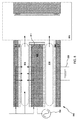
図2は、RPSの例示的機能構成要素の断面を図示する。RPS202は、少なくとも部分的に、チャンバ壁によって封入され、処理チャンバ206に結合するように構成される、RPSチャンバ203を含む。チャンバ壁は、第1の電極210および第2の電極212を分離することができ、第1の電極210は、RPSチャンバ203内に配置される。第2の電極212はまた、少なくとも部分的に、第1の電極210に対向する、または少なくとも部分的に、それを囲む(例えば、取り囲む)と言える。いくつかの実施形態では、RPSチャンバ203の壁は、第2の電極212の内側表面である。RF電源204は、RF電力(例えば、任意の時変電力)をRF電源入力205に、次いで、第1の電極210に提供する一方、第2の電極212は、随意の接地経路208を介して、接地されるか、または浮動である。RF電力は、主に、第2の電極212(いくつかの誘導結合もまた、生じ得る)と、RPSチャンバ203の少なくとも一部内で点火され、持続される、プラズマ216とに、静電的に(容量的に)結合される。
FIG. 2 illustrates a cross section of exemplary functional components of the RPS. The
RPS202は、プラズマ216と第1の電極210とが、異なる電位で動作し得るように、第1の電極210をプラズマ216から分離し、第1の電極210をプラズマ216からDC絶縁する第1の誘電構成要素220(例えば、セラミック)を含むことができる。第1の誘電構成要素220はまた、プラズマ216が、第1の電極210と相互作用することを防止するように配置されることができる。RPS202はまた、プラズマ216と第2の電極212とが、異なる電位で動作し得るように、第2の電極212をプラズマ216から分離し、第2の電極212をプラズマ216からDC絶縁する、第2の誘電構成要素222(例えば、セラミック)を含むことができる。第2の誘電構成要素222はまた、プラズマ216が、第2の電極212と相互作用することを防止するように配置されることができる。
The
十分な電力密度において、または2つの電極210、212間の電場強度が、十分に高いとき、第1と第2の誘電構成要素220、222間の流体(ガス、液体、または2つの組み合わせ)は、プラズマ216をイオン化し、形成する。流体は、物質の相の部分集合であり、ガス(任意の粘度)、液体、およびプラズマを含む。プラズマ216を点火する同じRF電力もまた、プラズマ216を容量的に持続させることができる。第1の流体(ガス、液体、または2つの組み合わせ)、例えば、非活性ガスは、第1の経路、例えば、軸方向流入経路218a、内側に向いた半径方向流入経路218b、または外側に向いた半径方向流入経路218cを介して、RPS202中に通されることができる。第1の経路は、第1の流体がチャンバ203中に通り、最適位置(例えば、最大プラズマ216の密度のエリア;第1と第2の電極210、212との間のエリア;最大流体−プラズマ相互作用が存在するエリア)で、プラズマ216と相互作用することを可能にする。第1の流体は、プラズマ216と相互作用し、第2の流体(ガス、液体、または2つの組み合わせ)、例えば、活性ガスおよび/または遊離基を形成するように解離し、第2の経路を介して、処理チャンバ206に通されることができる。第2の流体は、第1の流体から発生した解離流体の少なくとも一部を含むことができる。第2の経路は、例えば、1つ以上の流出経路219として実装されることができる。
At a sufficient power density or when the electric field strength between the two electrodes 210, 212 is sufficiently high, the fluid (gas, liquid, or combination of the two) between the first and second
本開示の目的のために、プラズマは、所望のプラズマ密度(また、電子またはイオン密度としても知られる)を維持することによって、または所望の値によって、電子−イオンの再結合率を超えるイオン化率を維持することによって持続される。ある実施形態では、プラズマは、プラズマ密度108〜1013自由電子/CM3が存在する場合、持続される。 For purposes of this disclosure, the plasma is an ionization rate that exceeds the electron-ion recombination rate by maintaining a desired plasma density (also known as electron or ion density) or by a desired value. Is maintained by maintaining In certain embodiments, the plasma is sustained when a plasma density of 10 8 to 10 13 free electrons / CM 3 is present.
ガスが、プラズマ216を通過するにつれて、RPS202と流体連通する処理チャンバ206に提供され得る活性ガスおよび/または遊離基を形成するように解離する。活性ガスおよび/または遊離基は、処理チャンバ206内の表面(例えば、チャンバ壁またはチャック搭載ウエハ224)と相互作用し、種々のプロセス、例えば、清浄およびエッチングを行うことができる。
As the gas passes through the
誘電構成要素220、222は、種々の形態をとることができる。例えば、誘電構成要素220、222は、電極210、212上に加工される化学層または障壁であることができる(例えば、エピタキシャル成長、酸化、スプレーコーティングを介して)。それらはまた、電極210、212と別個であるが、例えば、接続フランジ(図示せず)を介して、それに取り付けられる構造であることができる。いくつかの実施形態では、誘電構成要素220、222は、相互に結合されることができるが、しかしながら、それらは、典型的には、相互にDC絶縁される。
The
電極210、212および誘電構成要素220、222は、全て、内側構成要素(第1の電極210および第1の誘電構成要素220)を取り囲む、外側構成要素(第2の電極212および第2の誘電構成要素222)を伴う、種々の形状をとることができる。一事例では、RPS202は、管状または円筒形形状を有することができる。言い換えると、ウエハ224の観点から見ると、RPS202は、中心における第1の電極210と、外側リングを形成する第2の電極212とを伴う、一組のリングに見える。別の実施形態では、傾斜した縁を有する長方形を使用することができる(ウエハ224に対して傾斜した角を伴う一組の正方形に見える)。これらの構成要素は、同軸方向に整合される(例えば、同心円状)ことができるが、いくつかの実施形態では、2つの電極は、同じ軸を共有する必要はない(同心円状である必要はない)。
The electrodes 210, 212 and the
第1および第2の電極210、212は、例えば、第1の電極210が処理チャンバ206と交わる場所に、鋭い縁を有するように図示されるが、多くの実施形態では、これらの鋭い縁は、傾斜されまたは湾曲されることができる(例えば、図8における要素811参照)。これは、導体上の鋭い縁が、それらの縁または角近傍の電場密度を増加させる傾向にあるためであり、これは、RPS202における非均一電場密度につながる。非均一電場密度は、「ホットスポット」につながるか、またはRPS202の一部は、プラズマ216からより大きなイオン衝突を被り、したがって、RPS202の他の部分より早く浸食する。電極210、212の縁を湾曲させる、したがって、より均一な電場密度を確立することによって、RPS202は、ホットスポットを被らず、交換が要求されるまでの寿命が延長される。一実施形態では、第1の電極210の縁に対する曲率半径240は、実質的に、第1の電極の半径242と等しく、第2の電極212の縁に対する曲率半径244は、実質的に、第2の電極212の半径246と等しい。
Although the first and second electrodes 210, 212 are illustrated as having sharp edges, for example, where the first electrode 210 intersects the
軸方向経路218aならびに内側に向いたおよび外側に向いた半径方向経路218b、218cはそれぞれ、第1の経路の絶対的方向、配置、数、または構成ではなく、第1の流体に対する流動の相対的方向を図示する。いくつかの実施形態では、第1の経路は、電極210、212、誘電構成要素220、222、および/またはRPS202内に開口部を含み、第1の流体(例えば、加圧された非活性ガス)をRPS202に流入させ、プラズマ216と相互作用させることができる。いくつかの実施形態では、第1の流体は、異なる経路を通って、チャンバ203中に通る、複数の流体を含むことができる。したがって、複数の流体は、プラズマ216の異なる部分と相互作用することができる。
The axial path 218a and the inward and outward
経路218a、218b、218cは、RPS202の上半分にのみ流入するように図示されるが、RPS202の下半分上の経路インジケータの省略は、単に、図を簡略化するためである。当業者は、経路218a、218b、218cが、第1の流体がプラズマ216を通して、等しく分布されるように、RPS202全体の周囲に配置されることができることを認識するであろう。一方、いくつかの実施形態では、経路218a、218b、218cは、第1の流体が、RPSチャンバ203中に非均一に分配されるように配置されることができる。例えば、第1の流体は、RPSチャンバ203の中心の周囲に半径方向に分配される一方、RPSチャンバ203の端部近傍には分配されないことができる。
Although the
いくつかの実施形態では、第1の流体は、1つ以上の流体、例えば、ガス、液体、または2つの組み合わせを含むことができる。第2の流体もまた、1つ以上の流体、例えば、ガス、液体、または2つの組み合わせを含むことができる。いくつかの事例では、第1および第2の流体の一部または全部が、同じ流体であることができる。例えば、非活性ガスは、第1の流体として、チャンバ203内に流入し、部分的に、プラズマ216内で解離し、活性ガスおよび/または遊離基を形成し得る。これらは、第2の流体として、第1の流体(例えば、非活性ガス)の一部とともに、処理チャンバ206に通されることができ、第2の流体は、第1の流体の一部ならびにいくつかの活性ガスおよび/または遊離基を備えている。
In some embodiments, the first fluid can include one or more fluids, eg, gas, liquid, or a combination of the two. The second fluid can also include one or more fluids, eg, gas, liquid, or a combination of the two. In some cases, some or all of the first and second fluids can be the same fluid. For example, the non-active gas may flow into the
プラズマ216の境界は、この境界位置が、その定義に応じて変動するので、点線によって指定され、必ずしも、正確な縮尺で描かれていない。プラズマ216の境界は、範囲108〜1013の自由電子/CM3から選択されるプラズマ密度として、定義され得る。言い換えると、プラズマ216の境界内の全場所において、少なくとも108〜1013の自由電子/CM3が存在し得る。
The boundary of the
多くの実装では、電源204は、プラズマ216に点火し、持続させる、交流電圧を提供するVHF電源(例えば、実質的に、13.6MHZを上回る)によって実現される。比較的に高周波数(例えば、実質的に、13.6MHZを上回る)での動作は、第1の電極210に印加される電圧を減少させ、電力効率を改善し、RPSチャンバ203の壁の浸食を低減させることが可能であることが分かっている。ある範囲の周波数が利用され得(例えば、限定としてではないが、60MHZを含む)、本明細書にさらに論じられるように、2つ以上の電源204もまた、第1の電極210に電力を印加するために利用され得る。例えば、追加の電源(図示せず)(例えば、2MHZ電力供給源)によって、第1の電極210に追加の電力を印加することは、修正されたプラズマ216の密度分布を産生し、単一源または周波数が、第1の電極210に印加される事例より望ましくあり得ることが分かっている。
In many implementations, the
電源は、時として、少なくとも部分的に、非給電電極(図3、5、7、9)に対向する、または少なくとも部分的に、それを囲む(例えば、取り囲む)電極に、RF電力を電極に供給するように図示されるであろうが、他の事例では、ヒトが、給電または非接地または非浮動電極と接触することを回避するために、電源を内側電極に結合することが、好ましくあり得る(例えば、図2、4、6、8)。言い換えると、RF電力が、内側電極に供給されるとき、高電圧とのヒト接触は、可能性が低い。 The power supply is sometimes at least partially opposed to, or at least partially, surrounding (eg, surrounding) the non-powered electrode (FIGS. 3, 5, 7, 9) and RF power to the electrode. Although illustrated as being supplied, in other cases it may be preferable to couple a power supply to the inner electrode to avoid human contact with the powered or non-grounded or non-floating electrodes. Obtain (eg, FIGS. 2, 4, 6, 8). In other words, human contact with high voltage is unlikely when RF power is supplied to the inner electrode.
プラズマ216は、RPSチャンバ203の一部または全体内で点火され、持続されることができる。いくつかの実施形態では、プラズマ216は、RPS202の外側でさえ持続されることができ、例えば、プラズマ216は、処理チャンバ206中に拡張する。
The
本明細書に開示されるRPS202は、線形およびトロイダル源と比較して、いくつかの利点を有する。第1に、RPS202の長寿命が、「ホットスポット」を回避し、RPSチャンバ203内でより均一な電場の分布を達成することによって、可能となることである。これは、RPSチャンバ203内の均一電場および電力密度の維持を伴う。前述のように、電極210、212の湾曲された縁の使用は、電場および電力均一性を向上させる方法の1つである。第2に、電極210、212のうちの少なくとも1つに対する、浮動するプラズマ216の電位によって可能にされるように、イオン衝突が減少されることである。誘電構成要素220、222は、プラズマ216と電極210、212の一方または両方との間にDC絶縁を生成し、したがって、プラズマ216の電位が電極210、212の一方または両方に対して浮動することを可能にする。プラズマ216の電位が浮動することによって、シース電圧がより低くなり、したがって、RPSチャンバ203の壁に損傷を及ぼすイオン衝突が少ない。チャンバ203損傷を低下させることはまた、より低い局所電力によって可能となる(例えば、同じ電力が、システム中に入力されるが、局所高電力領域が、当技術分野におけるものほどひどくない)。言い換えると、静電RPS202は、誘導結合された源と同じプラズマ216の密度を持続することができるが、チャンバ203の壁損傷が少ない。この利点を別の方法で説明すると、DC電位(シース電位に見える)をRF電位から分離することによって、より強力なシース電圧に向けられ、したがって、より短いチャンバ203寿命となるのではなく、より多くのエネルギーが、プラズマ216の密度に向けられることができる。
The
1つ以上の誘電構成要素220、222はまた、チャンバ203の壁と活性ガスおよび遊離基との相互作用、ならびにプラズマ216の汚染を低減させる。プラズマ216の汚染は、先行技術では、プラズマが、金属チャンバ壁に飛び跳ね、プラズマ中に汚染物質を放出させる場合、生じ得る。当技術分野におけるチャンバ飛び跳ねの原因の1つは、2つの接地される電位間のチャンバ壁の表面を電流が流れる、接地アークである。1つ以上の誘電構成要素220、222は、接地アークを回避するのに役立ち得る。
One or more
電極210、212の配置もまた、当技術分野において可能ではなかった位置および角度において、非活性ガスが、プラズマ216に流入することを可能にする。例えば、トロイダルおよび線形誘導源は、RPS202では可能なように、外側に向いた半径方向経路218cを提供することは不可能である。第1の電極210の導入は、流体の通路のための新しい通路および配置ならびに他の機能、例えば、冷却を提供する。
The placement of the electrodes 210, 212 also allows non-active gas to flow into the
RPS202の別の利点は、多くの場合、誘導的に結合された源において要求される、変圧器の回避である。RPS202はまた、典型的には、当技術分野における源より高い周波数(例えば、>30MHZ、>160MHZ)で動作することができる。これらのより高い周波数では、プラズマ216を点火および持続させるために使用される電圧は、より低くなり、イオン衝突によるチャンバ壁損傷の減少につながる。言い換えると、容量RPS202では、より高い周波数において、より多くの割合の電力が、シース電圧ではなく、プラズマ216の密度の増加に投入される。この同じ利点は、誘導源では生じず、代わりに、周波数増加は、単に、より多くの電力をシース電圧に加え、したがって、チャンバ浸食が多くなる。
Another advantage of
より高い周波数(例えば、>30MHZ)で動作する容量結合されたRPS202は、RPS202が、当技術分野における源より広い点火および動作範囲を有することを可能にする(例えば、圧力、流量、電力、および/または周波数に対してより広範囲の容認可能パラメータ)。例えば、RPS202は、先行技術源と同じ圧力であるが、より低い電力で動作することができ、低電力処理用途において有利であり得る。先行技術源は、典型的には、RPS202と同じ電力および圧力でプラズマを持続できない。
Capacitively coupled
容量結合されたRPS202はまた、シャワーヘッドタイプの原位置源より小さい専有エリアを有し、誘導源と類似する専有エリアを有する。しかしながら、同じRPS202の専有エリアは、種々の処理チャンバ206のサイズのために使用することができる(例えば、処理チャンバ206が、より大きなウエハを収容するために増加される場合)一方、誘導遠隔源およびシャワーヘッド原位置源は、典型的には、より大きな処理チャンバを収容するために、サイズを増加させる。RPS202はまた、処理チャンバ206の外部に搭載され、設置および保守のために有利であり得る。
The capacitively coupled
RPS202はまた、ラック搭載VHF電源204および統合された整合ネットワーク回路(固定または選択可能のいずれか)を可能にする。RPS202はまた、掃引周波数インピーダンス整合を行うことができ、統合された点火回路を含むことができる。これは、有利には、多くの場合、別個の点火ならびに動作手順および回路を有する、誘導遠隔源に匹敵する。
The
誘導源内のコーティングおよび誘電体は、典型的には、プラズマへの結合効率を最大限にするように最適化される(例えば、より薄い誘電層を介して)。対照的に、RPS202は、誘電構成要素220、222が、材料タイプまたは厚さに修正を受けても、結合の減少を被らない。これは、誘電構成要素220、222が、結合効率を劣化させずに、より良好にある処理結果をもたらすために、修正されることを可能にする。
The coating and dielectric in the induction source are typically optimized to maximize the coupling efficiency to the plasma (eg, through a thinner dielectric layer). In contrast,
RPS202のための動作電力は、限定されないが、範囲100〜7000ワット、および10mトル〜200トルの圧力範囲を含むことができる。プラズマ216の密度は、1011−1012/cm3の範囲を含むことができ、プラズマ216は、ある実施形態では、RPS源チャンバ203を越えて、処理チャンバ206中に拡張または投出されるようにすることができる(また、遠隔投影プラズマ源としても知られる)。プラズマ216の密度は、例えば、主要放電領域にわたる平均としてのプラズマ216のバルクの測定値であることができる。主要放電領域は、チャンバ203の少なくとも一部を含むことができ、いくつかの実施形態では、処理チャンバ206中に拡張することができる。
The operating power for the
RPS202の別の利点は、電極210、212の一方が、接地されるか、または浮動であることができるため、ウエハ224が、接地される必要がなく、したがって、独特の処理(例えば、窒化物表面の作製、低エネルギーエッチング、または表面修正)を可能にすることである。言い換えると、RPS202を使用することによって、ウエハ224は、任意の所望の電位において、浮動またはバイアスされ得る(RF回路の一部である必要はない)。これは、接地懸念およびVHFチャンバ203の適合性を緩和し、さらに、ウエハ224のVHFプラズマ処理を可能にする。この技術は、また、後方適用性があり、したがって、修正せずに、古い処理チャンバ206と使用することができる。
Another advantage of the
ウエハ224が、本明細書では、図示および説明されるが、当業者は、種々の他の処理標的が、ウエハ224に代用され得ることを認識するであろう。例えば、ガラスシート(例えば、LCD、LED、およびプラズマテレビ製品用)が、処理チャンバ206内で処理されることができる。
Although
図2に描写される構成要素は、多くの実施形態に関連付けられた機能構成要素を伝えることを意図する。そのうちのいくつかは、本明細書でさらに論じられる。図2におけるこれらの構成要素の描写は、機械的または電気的ハードウェア略図であることを意図しない。したがって、描写される構成要素は、並べ替えられ、修正される一方、依然として、同じ機能性を提供し得る。さらに、いくつかの構成要素は、組み合わせられ、または除去され得、追加の構成要素が、種々の実装において追加され得る。例えば、電極210、212の幾何学的側面および相対的位置付けは、実質的に、実施形態毎に変動し得る。また、電源204は、整合ネットワーク(例えば、図1における108)を伴わずに図示される。しかしながら、当業者は、電源204が、インピーダンス整合回路を含むことが想定され得ることを認識するであろう。電源204は、第1の電極210に結合されるが、電源204は、代替として、第2の電極212に連結されることができ、第1の電極210は、接地または浮動されることができる(図3参照)。2つの誘電構成要素220、222が示されるが、いくつかの実施形態では、単一誘電構成要素のみ、使用される(図4−7参照)。3つの流入経路218a、218b、218cが、図示されるが、実際は、これらの経路のうちの1つ以上のみ、使用することができる。電極210、212は、同じ長さを有するように図示されるが、いくつかの実施形態では、RF電力を電源204から受電する電極(給電電極)は、接地または浮動電極より短い(図8−9参照)。
The components depicted in FIG. 2 are intended to convey functional components associated with many embodiments. Some of them are discussed further herein. The depiction of these components in FIG. 2 is not intended to be a mechanical or electrical hardware schematic. Thus, the depicted components can be rearranged and modified while still providing the same functionality. In addition, some components may be combined or removed, and additional components may be added in various implementations. For example, the geometrical aspects and relative positioning of the electrodes 210, 212 can vary substantially from embodiment to embodiment. Also, the
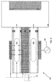
図3は、RPS302の実施形態を図示し、RF電力は、少なくとも部分的に、内側電極310を囲む外側電極312に提供され、内側電極310は、随意の接地接続308を介して接地され、または電気的に浮動であることができる。RPS302はまた、内側電極310をプラズマ316から分離する、第1の誘電構成要素320を含む。RPS302はさらに、外側電極312をプラズマ316から分離する、第2の誘電構成要素322を含む。
FIG. 3 illustrates an embodiment of
図4は、RPS402の実施形態を図示し、RF電力は、少なくとも部分的に、外側電極412によって囲まれる、内側電極410に提供され、外側電極412は、随意の接地接続408を介して接続され、または電気的に浮動であることができる。RPS402はまた、外側電極412をプラズマ416から分離する、第1の誘電構成要素420を含む。
FIG. 4 illustrates an embodiment of
図5は、RPS502の実施形態を図示し、RF電力は、内側電極510を取り囲む、外側電極512に提供され、内側電極510は、随意の接地接続508を介して、接地される、または電気的に浮動であることができる。RPS502はまた、外側電極512をプラズマ516から分離する、第1の誘電構成要素520を含む。
FIG. 5 illustrates an embodiment of
図6は、RPS602の実施形態を図示し、RF電力は、少なくとも部分的に、外側電極612によって囲まれる、内側電極610に提供され、外側電極612は、随意の接地接続608を介して、接地され、または電気的に浮動であることができる。RPS602はまた、内側電極610をプラズマ616から分離する、第1の誘電構成要素620を含む。
FIG. 6 illustrates an embodiment of
図7は、RPS702の実施形態を図示し、RF電力は、内側電極710を取り囲む、外側電極712に提供され、内側電極710は、随意の接地接続708を介して、接地され、または電気的に浮動されることができる。RPS702はまた、内側電極710およびプラズマ716を分離する、第1の誘電構成要素720を含む。
FIG. 7 illustrates an embodiment of an
図8は、RPS802の実施形態を図示し、RF電力は、少なくとも部分的に、第2の電極812(外側電極)によって囲まれる、第1の電極810(内側電極)に提供される。第2の電極812は、随意の接地接続808を介して、接地され、または電気的に浮動であることができる。RPS802はまた、第1の電極810をプラズマ816から分離する、第1の誘電構成要素820と、第2の電極812をプラズマ816から分離する、第2の誘電構成要素822を含む。第1の電極810は、第2の電極812より短い(あまり長くない)。言い換えると、電源804(給電電極)を介して給電される電極は、非給電(接地または浮動)電極より短い。これらの同じラインに沿って、第1の誘電構成要素820は、第1の電極810の正面の周りを巻く。言い換えると、第1の電極810およびプラズマ816の全部分間に、誘電障壁を提供する。
FIG. 8 illustrates an embodiment of
第1の電極810は、第2の電極812ほど長くない。例えば、第1の電極810は、実施例としていくつか挙げると、第2の電極812の長さの90%、80%、50%、または25%であることができる。いくつかの事例では、第1の電極810は、その直径または半径より短い、長さを有することができる。そのような場合、プラズマ816は、第1の電極810を封入するのではなく、より管状に成形される。
The first electrode 810 is not as long as the second electrode 812. For example, the first electrode 810 can be 90%, 80%, 50%, or 25% of the length of the second electrode 812, to name a few. In some cases, the first electrode 810 can have a length that is less than its diameter or radius. In such a case, the
図示されるように、第1の電極810は、処理チャンバ806の近位において鋭い縁を有する。しかしながら、他の実施形態では、これらの縁は、湾曲または傾斜されることができ(点線811によって示されるように)、特に、実質的に、第1の電極810の直径の半分に等しい、半径を有するように、湾曲されることができる。
As shown, the first electrode 810 has a sharp edge proximal to the
図9は、RPS902の実施形態を図示し、RF電力は、第1の電極910(内側電極)を取り囲む、第2の電極912(外側電極)に提供される。内側電極910は、随意の接地接続908を介して、接地され、または電気的に浮動であることができる。RPS902はまた、第1の電極910をプラズマ916から分離する、第1の誘電構成要素920と、第2の電極912をプラズマ916から分離する、第2の誘電構成要素922とを含む。第2の電極912は、第1の電極910より短い(あまり長くない)。言い換えると、電源904(給電電極)を介して給電される電極は、非給電(接地または浮動)電極より短い。第1および第2の誘電構成要素920、922は、均等長を有するように図示されるが、いくつかの実施形態では、これらの長さは、等しくある必要はない。
FIG. 9 illustrates an embodiment of
RPS902は、少なくとも部分的に、第1および第2の誘電構成要素920、922によって封入され得る、チャンバ903を含む。プラズマ916は、第2の電極912によって囲まれる、チャンバ903の一部内に閉じ込められることができる。プラズマ916の一部は、第2の電極912の閉じ込めを越えて拡張することができるが、典型的には、チャンバ903の長さにわたって延在せず、または例えば、処理チャンバ906中まで延在しない。
The
閉じ込めは、典型的には、プラズマ916が、電極910、912が重複する、RPSチャンバ903の領域内に閉じ込められるものとして図示される。例えば、図9のプラズマ916は、主に、第2の電極912がより長い第1の電極910に重複するRPSチャンバ903のその領域に閉じ込められる。
Confinement is typically illustrated as the
内側電極が接地される、前述の種々の実施形態では、RPSは、追加の利点を有する。すなわち、外側に向いた半径方向流入経路を介して流入する非活性ガスは、導入点(例えば、給電電極とチャンバとの間)の電位差を横断する必要はない。 In the various embodiments described above where the inner electrode is grounded, the RPS has additional advantages. That is, the inert gas flowing in through the outward radial inflow path need not cross the potential difference at the introduction point (eg, between the feed electrode and the chamber).
全図示される実施形態では、第1の電極と第2の電極との間の半径方向距離は、電流が、主に、プラズマを介して、電極間を通過するように十分に小さい。言い換えると、電極間の領域(例えば、チャンバ203)は、低電力動作モードにおいて、好ましい電流経路であることができる。電力または圧力が、増加される場合、または種々のプラズマ特性が、改変される場合、任意の電位における任意の他の導体または電極が、三次電極として作用することができ、電極と本第3の電極との間のプラズマのための「拡張区域」を生成または拡張するために使用することができる。例えば、ポンピングプレナムまたはチャンバの壁が接地され、したがって、第3の電極として作用することができ、プラズマは、この第3の電極に向かって拡張する。プラズマを高電場強度の領域外に拡張させることによって、種々の利点を達成することができる。1つは、活性ガスおよび遊離基が、より低い電場強度が存在する拡張区域内のプラズマ中に形成され得、これは、そうでなければ、典型的プラズマ領域内で形成が困難または不可能である。別の1つは、例えば、異なる種が、異なる寿命を有する場合、拡張区域内のプラズマを使用して、望ましくない活性ガスおよび遊離基を濾過または除去することができる。拡張区域はまた、RF電力が印加されるボリュームを拡張させ、したがって、局所電力密度を減少させ、冷却の解決策を単純化する。 In all illustrated embodiments, the radial distance between the first electrode and the second electrode is sufficiently small so that current passes between the electrodes, primarily through the plasma. In other words, the region between the electrodes (eg, chamber 203) can be the preferred current path in the low power mode of operation. If power or pressure is increased, or if various plasma properties are modified, any other conductor or electrode at any potential can act as a tertiary electrode, and the electrode and third It can be used to create or expand an “expansion zone” for the plasma between the electrodes. For example, the pumping plenum or chamber wall is grounded and can thus act as a third electrode, and the plasma expands towards this third electrode. Various advantages can be achieved by extending the plasma out of the region of high electric field strength. For one, active gases and free radicals can be formed in a plasma in an extended zone where lower electric field strength exists, which is otherwise difficult or impossible to form in a typical plasma region. is there. Another is, for example, where different species have different lifetimes, the plasma in the extended zone can be used to filter or remove unwanted active gases and free radicals. The extended area also expands the volume to which RF power is applied, thus reducing the local power density and simplifying the cooling solution.
本開示における電極は、多くの場合、第1および第2の電極として説明され、第1の電極は、少なくとも部分的に、第2の電極によって囲まれるように図示されたが、これらの配置は、第1の電極が、少なくとも部分的に、第2の電極を囲むように、反対にされることができる。 Although the electrodes in this disclosure are often described as first and second electrodes, and the first electrode is shown at least partially surrounded by the second electrode, these arrangements are The first electrode can be reversed so as to at least partially surround the second electrode.
図10は、容量結合された遠隔プラズマ源内でプラズマを持続させる方法を図示する。本方法は、図2の図要素を挿入的に参照して説明されるであろう。本方法は、第1の通過動作1002において、2つの容量結合された電極(例えば、210および212)間にRF電力を通すことを含む。電極は、容量結合された遠隔プラズマ源のチャンバ(例えば、203)を規定するチャンバ壁によって分離されることができる。本方法はさらに、持続動作1004において、チャンバ内にプラズマ(例えば、216)を持続させることを含む。プラズマは、プラズマに容量結合されているRF電力を介して、持続されることができる。第1の流体は、提供動作1006を介して、チャンバ中に提供されることができる(例えば、半径方向にまたは軸方向に)。第1の流体が、プラズマと相互作用するにつれて、第1の流体の少なくとも一部は、解離動作1008において、解離し、活性ガスおよび/または遊離基を形成することができる。活性ガスおよび/または遊離基と、時として、第1の流体の一部を備えている第2の流体は、次いで、第2の通過動作1010において、容量結合された遠隔プラズマ源に結合される処理チャンバへ通ることができる。
FIG. 10 illustrates a method for sustaining a plasma in a capacitively coupled remote plasma source. The method will be described with additional reference to the diagram elements of FIG. The method includes passing RF power between two capacitively coupled electrodes (eg, 210 and 212) in a
本明細書に説明されるシステムおよび方法は、本明細書に説明される具体的物理的デバイスに加え、機械、例えば、コンピュータシステム内に実装することができる。図11は、コンピュータシステム1100の例示的形態における、機械の一実施形態の概略表現を示し、その中で、一組の命令によって、デバイスに、本開示の側面および/または方法論のうちの任意の1つ以上を実施あるいは実行させることができる。図11における構成要素は、実施例にすぎず、任意のハードウェア、ソフトウェア、埋込論理構成要素、または特定の実施形態を実装する、2つ以上のそのような構成要素の組み合わせの使用または機能性の範囲を限定しない。
The systems and methods described herein can be implemented in machines, eg, computer systems, in addition to the specific physical devices described herein. FIG. 11 shows a schematic representation of an embodiment of a machine in an exemplary form of a
コンピュータシステム1100は、プロセッサ1101と、メモリ1103と、バス1140を介して、相互におよび他の構成要素と通信する、記憶装置1108とを含み得る。バス1140はまた、ディスプレイ1132、1つ以上の入力デバイス1133(例えば、キーパッド、キーボード、マウス、スタイラス等を含み得る)、1つ以上の出力デバイス1134、1つ以上の記憶デバイス1135、および種々の有形記憶媒体1136をリンクし得る。これらの要素は全て、直接、あるいは1つ以上のインターフェースまたはアダプタを介して、バス1140とインターフェースをとり得る。例えば、種々の有形記憶媒体1136は、記憶媒体インターフェース1126を介して、バス1140とインターフェースをとることができる。コンピュータシステム1100は、1つ以上の集積回路(IC)、印刷回路基板(PCB)、モバイルハンドヘルドデバイス(例えば、携帯電話またはPDA)、ラップトップまたはノートブックコンピュータ、分散型コンピュータシステム、コンピューティンググリッド、またはサーバを含むが、それらに限定されない、任意の好適な物理的形態を有し得る。
プロセッサ1101(例えば、中央処理ユニット(CPU))は、随意に、命令、データ、またはコンピュータアドレスの一時的ローカル記憶のためのキャッシュメモリユニット1102を含む。プロセッサ1101は、コンピュータ可読命令の実行を補助するように構成される。コンピュータシステム1100は、プロセッサ1101が、1つ以上の有形コンピュータ可読記憶媒体、例えば、メモリ1103、記憶装置1108、記憶デバイス1135、および/または記憶媒体1136内で具現化されるソフトウェアを実行する結果として、機能性を提供し得る。コンピュータ可読媒体は、特定の実施形態を実装する、ソフトウェアを記憶し得、プロセッサ1101は、ソフトウェアを実行し得る。メモリ1103は、1つ以上の他のコンピュータ可読媒体(例えば、大容量記憶デバイス1135、1136)または1つ以上の他の源から、好適なインターフェース、例えば、ネットワークインターフェース1120を通して、ソフトウェアを読み取り得る。ソフトウェアは、プロセッサ1101に、本明細書に説明または図示される、1つ以上のプロセスあるいは1つ以上のプロセスの1つ以上のステップを行わせ得る。そのようなプロセスまたはステップを行うことは、メモリ1103内に記憶されたデータ構造を定義することと、ソフトウェアによって指示されるように、データ構造を修正することとを含み得る。
A processor 1101 (eg, a central processing unit (CPU)) optionally includes a
メモリ1103は、限定されないが、ランダムアクセスメモリ構成要素(例えば、RAM1104)(例えば、静的RAM「SRAM」、動的RAM「DRAM等」、読取専用構成要素(例えば、ROM1105)、および任意のそれらの組み合わせを含む、種々の構成要素(例えば、機械可読媒体)を含み得る。ROM1105は、一方向に、データおよび命令をプロセッサ1101に通信するように作用し得、RAM1104は、双方向に、データおよび命令をプロセッサ1101と通信するように作用し得る。ROM1105およびRAM1104は、以下に説明される、任意の好適な有形コンピュータ可読媒体を含み得る。一実施例では、例えば、起動の際、コンピュータシステム1100内の要素間で情報を転送するのに役立つ、基本ルーチンを含む、基本入/出力システム1106(BIOS)が、メモリ1103内に記憶され得る。
The
固定記憶装置1108は、随意に、記憶制御ユニット1107を通して、双方向に、プロセッサ1101に接続される。固定記憶装置1108は、追加のデータ記憶容量を提供し、また、本明細書に説明される任意の好適な有形コンピュータ可読媒体を含み得る。記憶装置1108は、オペレーティングシステム1109、EXEC1110(実行ファイル)、データ1111、APVアプリケーション1112(アプリケーションプログラム)、および同等物を記憶するために使用され得る。多くの場合、常時ではないが、記憶装置1108は、一次記憶(例えば、メモリ1103)より低速である、二次記憶装置媒体(例えば、ハードディスク)である。記憶装置1108はまた、光ディスクドライブ、固体メモリデバイス(例えば、フラッシュベースのシステム)、または前述の任意の組み合わせを含むことができる。記憶装置1108内の情報は、適切な場合、メモリ1103内の仮想メモリとして組み込まれ得る。
一実施例では、記憶デバイス1135は、記憶デバイスインターフェース1125を介して、コンピュータシステム1100と可撤性にインターフェースがとられ得る(例えば、外部ポートコネクタ(図示せず)を介して)。特に、記憶デバイス1135および関連付けられた機械可読媒体は、機械可読命令、データ構造、プログラムモジュール、および/またはコンピュータシステム1100のための他のデータの不揮発性および/または揮発性記憶を提供し得る。一実施例では、ソフトウェアは、完全にまたは部分的に、記憶デバイス1135上の機械可読媒体内に常駐し得る。別の実施例では、ソフトウェアは、完全にまたは部分的に、プロセッサ1101内に常駐し得る。
In one embodiment,
バス1140は、種々のサブシステムを接続する。ここでは、バスの参照は、必要に応じて、共通機能を果たす、1つ以上のデジタル信号ラインを包含し得る。バス1140は、限定されないが、メモリバス、メモリコントローラ、周辺バス、ローカルバス、および種々のバスアーキテクチャのいずれかを使用する任意のそれらの組み合わせを含む、いくつかのタイプのバス構造のいずれかであり得る。限定ではなく、実施例として、そのようなアーキテクチャとして、業界標準アーキテクチャ(ISA)バス、拡張ISA(EISA)バス、マイクロチャネルアーキテクチャ(MCA)バス、ビデオエレクトロニクス規格協会ローカルバス(VLB)、周辺装置相互接続(PCI)バス、PCI−エクスプレス(PCI−X)バス、アクセラレーテッドグラフィックポート(AGP)バス、ハイパートランスポート(HTX)バス、シリアルアドバンストテクノロジーアタッチメント(SATA)バス、および任意のそれらの組み合わせが挙げられる。
A
コンピュータシステム1100はまた、入力デバイス1133を含み得る。一実施例では、コンピュータシステム1100のユーザは、入力デバイス1133を介して、コマンドおよび/または他の情報をコンピュータシステム1100に入力し得る。入力デバイス1133の実施例として、英数字入力デバイス(例えば、キーボード)、ポインティングデバイス(例えば、マウスまたはタッチパッド)、タッチパッド、ジョイスティック、ゲームパッド、オーディオ入力デバイス(例えば、マイクロホン、音声応答システム等)、光学スキャナ、ビデオまたは静止画捕捉デバイス(例えば、カメラ)、および任意のそれらの組み合わせが挙げられるが、それらに限定されない。入力デバイス1133は、限定されないが、シリアル、パラレル、ゲームポート、USB、FIREWIRE、THUNDERBOLT、または前述の任意の組み合わせを含む、種々の入力インターフェース1123(例えば、入力インターフェース1123)のいずれかを介して、バス1140にインターフェースがとられ得る。
特定の実施形態では、コンピュータシステム1100が、ネットワーク1130に接続されると、コンピュータシステム1100は、ネットワーク1130に接続された他のデバイス、具体的には、モバイルデバイスおよび企業システムと通信し得る。コンピュータシステム1100へおよびそこからの通信は、ネットワークインターフェース1120を通して送信され得る。例えば、ネットワークインターフェース1120は、ネットワーク1130から、1つ以上のパケット(例えば、インターネットプロトコル(IP)パケット)の形態において、着信通信(例えば、他のデバイスからの要求または応答)を受信し得、コンピュータシステム1100は、処理のために、メモリ1103内に着信通信を記憶し得る。コンピュータシステム1100は、同様に、メモリ1103内に、1つ以上のパケットの形態において、発信通信(例えば、他のデバイスへの要求または応答)を記憶し、ネットワークインターフェース1120から、ネットワーク1130に通信され得る。プロセッサ1101は、処理のために、メモリ1103内に記憶されたこれらの通信パケットにアクセスし得る。
In certain embodiments, when the
ネットワークインターフェース1120の実施例として、ネットワークインターフェースカード、モデム、および任意のそれらの組み合わせが挙げられるが、それらに限定されない。ネットワーク1130またはネットワークセグメント1130の実施例として、広域ネットワーク(WAN)(例えば、インターネット、企業ネットワーク)、ローカルエリアネットワーク(LAN)(例えば、オフィス、建物、キャンパス、または他の比較的に小さい地理的空間に関連付けられたネットワーク)、電話回線、2つのコンピューティングデバイス間の直接接続、および任意のそれらの組み合わせが挙げられるが、それらに限定されない。ネットワーク、例えば、ネットワーク1130は、有線および/または無線モードの通信を採用し得る。一般に、任意のネットワークトポロジが使用され得る。
Examples of
情報およびデータは、ディスプレイ1132を通して、表示されることができる。ディスプレイ1132の実施例として、液晶ディスプレイ(LCD)、有機液晶ディスプレイ(OLED)、ブラウン管(CRT)、プラズマディスプレイ、および任意のそれらの組み合わせが挙げられるが、それらに限定されない。ディスプレイ1132は、バス1140を介して、プロセッサ1101、メモリ1103、および固定記憶装置1108、ならびに他のデバイス、例えば、入力デバイス1133とインターフェースをとることができる。ディスプレイ1132は、ビデオインターフェース1122を介して、バス1140にリンクされ、ディスプレイ1132とバス1140との間のデータの転送は、グラフィック制御1121を介して、制御されることができる。
Information and data can be displayed through
ディスプレイ1132に加え、コンピュータシステム1100は、限定されないが、オーディオスピーカ、プリンタ、および任意のそれらの組み合わせを含む、1つ以上の他の周辺出力デバイス1134を含み得る。そのような周辺出力デバイスは、出力インターフェース1124を介して、バス1140に接続され得る。出力インターフェース1124の実施例として、シリアルポート、パラレル接続、USBポート、FIREWIREポート、THUNDERBOLTポート、および任意のそれらの組み合わせが挙げられるが、それらに限定されない。
In addition to
加えて、または代替として、コンピュータシステム1100は、ソフトウェアの代わりに、またはそれとともに、本明細書に説明または図示される、1つ以上のプロセスまたは1つ以上のプロセスの1つ以上のステップを実行するように動作し得る、回路内に配線される、または別様に具現化される、論理の結果として、機能性を提供し得る。本開示におけるソフトウェアの参照は、論理を包含し得、論理の参照は、ソフトウェアを包含し得る。さらに、コンピュータ可読媒体の参照は、必要に応じて、実行のためのソフトウェアを記憶する回路(例えば、IC)、実行のための論理を具現化する回路、または両方を包含し得る。本開示は、ハードウェア、ソフトウェア、または両方の任意の好適な組み合わせを包含する。
Additionally or alternatively, the
結論として、本発明は、とりわけ、遠隔プラズマ源内で容量結合されたプラズマを持続させるための方法、システム、および装置を提供する。当業者は、多数の変形例および代用が、実質的に、本明細書に説明される実施形態によって達成されるものと同じ結果を達成するために、本発明、その使用、ならびに構成において行われてもよいことを容易に認識することができる。故に、本発明を開示される例示的形態に限定する意図はない。多くの変形例、修正、および代替構造は、開示される発明の範囲および精神内にある。 In conclusion, the present invention provides, among other things, a method, system, and apparatus for sustaining a capacitively coupled plasma in a remote plasma source. Those skilled in the art will recognize that numerous variations and substitutions may be made in the present invention, its uses, and configurations to achieve substantially the same results as achieved by the embodiments described herein. Can be easily recognized. Accordingly, there is no intention to limit the invention to the disclosed exemplary forms. Many variations, modifications, and alternative constructions are within the scope and spirit of the disclosed invention.
Claims (14)
前記遠隔プラズマ源は、
第1の電極と、
第2の電極であって、前記第1または第2の電極の一方は、少なくとも部分的に、他方を囲む、第2の電極と、
少なくとも部分的に、チャンバ壁によって封入されているチャンバであって、前記チャンバは、大気圧未満処理チャンバに外部から結合されるように構成され、前記チャンバ壁は、前記第1および第2の電極を分離し、
前記チャンバは、
前記チャンバの中への第1の流体の流入のための第1の経路と、
第2の流体を前記処理チャンバに提供するように構成される、第2の経路であって、前記第2の流体は、前記第1の流体から生成された解離流体の少なくとも一部を含む、第2の経路と
を含む、チャンバと、
RF電源に結合するように構成されているRF電源入力であって、前記RF電源入力は、RF電力を前記RF電源から前記第1の電極に提供するように構成されており、前記RF電力は、前記第2の電極に静電的に結合することにより、前記チャンバの少なくとも一部内にプラズマを静電的に持続させる、RF電源入力と、
前記第1の電極を前記プラズマから分離する第1の誘電構成要素であって、前記第1の誘電構成要素は、前記第1の電極を前記プラズマからDC絶縁し、前記プラズマが前記第1の電極と相互作用することを防止する、第1の誘電構成要素と、
前記第2の電極を前記プラズマから分離する第2の誘電構成要素であって、前記第2の誘電構成要素は、前記第2の電極を前記プラズマからDC絶縁し、前記プラズマが前記第2の電極と相互作用することを防止する、第2の誘電構成要素と、
大気圧未満の圧力の範囲にわたる前記遠隔プラズマ源の動作を可能にするように前記RF電源および前記第1の電極に結合される制御可能なインピーダンス整合回路と
を備えている、遠隔プラズマ源。 A remote plasma source,
The remote plasma source is
A first electrode;
A second electrode, wherein one of the first or second electrodes at least partially surrounds the other;
A chamber that is at least partially enclosed by a chamber wall, the chamber configured to be externally coupled to a sub- atmospheric processing chamber , the chamber wall including the first and second electrodes Isolate
The chamber is
A first path for inflow of a first fluid into the chamber;
A second path configured to provide a second fluid to the processing chamber, the second fluid including at least a portion of a dissociating fluid generated from the first fluid; A chamber comprising: a second path;
A RF power input configured to be coupled to an RF power source, the RF power input is configured to provide RF power from the RF power source to the first electrode, the RF power An RF power input that electrostatically couples to the second electrode to electrostatically sustain a plasma within at least a portion of the chamber ;
A first dielectric component separating said first electrode from said plasma, said first dielectric component DC-insulating said first electrode from said plasma, said plasma being said first A first dielectric component that prevents interaction with the electrode;
A second dielectric component that separates the second electrode from the plasma, the second dielectric component DC-insulating the second electrode from the plasma, wherein the plasma is the second dielectric component. A second dielectric component that prevents interaction with the electrode;
A remote plasma source comprising a controllable impedance matching circuit coupled to the RF power source and the first electrode to allow operation of the remote plasma source over a range of pressures below atmospheric pressure .
前記方法は、
前記遠隔プラズマ源を処理チャンバに外部から搭載することと、
前記遠隔プラズマ源および前記処理チャンバで大気圧未満封入部を生成することと、
前記容量結合された遠隔プラズマ源のチャンバを少なくとも部分的に封入するチャンバ壁によって分離されている2つの容量結合された電極間にRF電源からのRF電力を通すことと、
前記プラズマに容量結合されている前記RF電力によって、前記チャンバ内でプラズマを持続させることと、
第1の流体を前記チャンバの中に提供することと、
前記プラズマとの相互作用によって、前記第1の流体の少なくとも一部を解離させることと、
第2の流体を前記容量結合された遠隔プラズマ源に結合された処理チャンバに通すことと、
前記第1の電極を前記プラズマから分離する第1の誘電構成要素によって、前記第1の電極を前記プラズマからDC絶縁することと、
前記第2の電極を前記プラズマから分離する第2の誘電構成要素によって、前記第2の電極を前記プラズマからDC絶縁することと、
大気圧未満の圧力の範囲にわたる前記遠隔プラズマ源の動作を可能にするように前記RF電源で前記プラズマのインピーダンスを選択可能に整合させることと
を含む、方法。 A method for sustaining a plasma in a capacitively coupled remote plasma source comprising:
The method
Mounting the remote plasma source externally to the processing chamber;
Generating a sub-atmospheric enclosure in the remote plasma source and the processing chamber;
Passing RF power from an RF power source between two capacitively coupled electrodes separated by a chamber wall that at least partially encloses the chamber of the capacitively coupled remote plasma source;
Sustaining the plasma in the chamber by the RF power capacitively coupled to the plasma;
Providing a first fluid into the chamber;
Dissociating at least a portion of the first fluid by interaction with the plasma;
Passing a second fluid through a processing chamber coupled to the capacitively coupled remote plasma source ;
DC isolating the first electrode from the plasma by a first dielectric component that separates the first electrode from the plasma;
DC isolating the second electrode from the plasma by a second dielectric component that separates the second electrode from the plasma;
Selectively matching the impedance of the plasma with the RF power source to allow operation of the remote plasma source over a range of pressures less than atmospheric pressure .
The method of claim 9 , wherein the chamber wall is an inner surface of one of the first or second electrodes.
Applications Claiming Priority (7)
| Application Number | Priority Date | Filing Date | Title |
|---|---|---|---|
| US201161436131P | 2011-01-25 | 2011-01-25 | |
| US61/436,131 | 2011-01-25 | ||
| US201161554536P | 2011-11-02 | 2011-11-02 | |
| US61/554,536 | 2011-11-02 | ||
| US13/356,546 | 2012-01-23 | ||
| US13/356,546 US8723423B2 (en) | 2011-01-25 | 2012-01-23 | Electrostatic remote plasma source |
| PCT/US2012/022380 WO2012103101A1 (en) | 2011-01-25 | 2012-01-24 | Electrostatic remote plasma source |
Related Child Applications (1)
| Application Number | Title | Priority Date | Filing Date |
|---|---|---|---|
| JP2016053343A Division JP2016149365A (en) | 2011-01-25 | 2016-03-17 | Electrostatic remote plasma source |
Publications (2)
| Publication Number | Publication Date |
|---|---|
| JP2014511543A JP2014511543A (en) | 2014-05-15 |
| JP5905906B2 true JP5905906B2 (en) | 2016-04-20 |
Family
ID=46543681
Family Applications (2)
| Application Number | Title | Priority Date | Filing Date |
|---|---|---|---|
| JP2013551290A Active JP5905906B2 (en) | 2011-01-25 | 2012-01-24 | Electrostatic remote plasma source |
| JP2016053343A Pending JP2016149365A (en) | 2011-01-25 | 2016-03-17 | Electrostatic remote plasma source |
Family Applications After (1)
| Application Number | Title | Priority Date | Filing Date |
|---|---|---|---|
| JP2016053343A Pending JP2016149365A (en) | 2011-01-25 | 2016-03-17 | Electrostatic remote plasma source |
Country Status (7)
| Country | Link |
|---|---|
| US (3) | US8723423B2 (en) |
| EP (1) | EP2668830A4 (en) |
| JP (2) | JP5905906B2 (en) |
| KR (1) | KR20140005244A (en) |
| CN (2) | CN107396526B (en) |
| TW (1) | TWI538570B (en) |
| WO (1) | WO2012103101A1 (en) |
Cited By (1)
| Publication number | Priority date | Publication date | Assignee | Title |
|---|---|---|---|---|
| JP2016149365A (en) * | 2011-01-25 | 2016-08-18 | アドバンスト・エナジー・インダストリーズ・インコーポレイテッドAdvanced Energy Industries, Inc. | Electrostatic remote plasma source |
Families Citing this family (173)
| Publication number | Priority date | Publication date | Assignee | Title |
|---|---|---|---|---|
| PL2790205T3 (en) | 2009-02-17 | 2018-10-31 | Solvix Gmbh | A power supply device for plasma processing |
| US9435029B2 (en) | 2010-08-29 | 2016-09-06 | Advanced Energy Industries, Inc. | Wafer chucking system for advanced plasma ion energy processing systems |
| US9287086B2 (en) | 2010-04-26 | 2016-03-15 | Advanced Energy Industries, Inc. | System, method and apparatus for controlling ion energy distribution |
| US9767988B2 (en) | 2010-08-29 | 2017-09-19 | Advanced Energy Industries, Inc. | Method of controlling the switched mode ion energy distribution system |
| US11615941B2 (en) | 2009-05-01 | 2023-03-28 | Advanced Energy Industries, Inc. | System, method, and apparatus for controlling ion energy distribution in plasma processing systems |
| US9287092B2 (en) * | 2009-05-01 | 2016-03-15 | Advanced Energy Industries, Inc. | Method and apparatus for controlling ion energy distribution |
| US8501631B2 (en) | 2009-11-19 | 2013-08-06 | Lam Research Corporation | Plasma processing system control based on RF voltage |
| US9309594B2 (en) | 2010-04-26 | 2016-04-12 | Advanced Energy Industries, Inc. | System, method and apparatus for controlling ion energy distribution of a projected plasma |
| US9362089B2 (en) | 2010-08-29 | 2016-06-07 | Advanced Energy Industries, Inc. | Method of controlling the switched mode ion energy distribution system |
| US10283321B2 (en) | 2011-01-18 | 2019-05-07 | Applied Materials, Inc. | Semiconductor processing system and methods using capacitively coupled plasma |
| US9220162B2 (en) * | 2011-03-09 | 2015-12-22 | Samsung Electronics Co., Ltd. | Plasma generating apparatus and plasma generating method |
| US8884525B2 (en) | 2011-03-22 | 2014-11-11 | Advanced Energy Industries, Inc. | Remote plasma source generating a disc-shaped plasma |
| US10225919B2 (en) | 2011-06-30 | 2019-03-05 | Aes Global Holdings, Pte. Ltd | Projected plasma source |
| US10325759B2 (en) | 2012-02-22 | 2019-06-18 | Lam Research Corporation | Multiple control modes |
| US9390893B2 (en) | 2012-02-22 | 2016-07-12 | Lam Research Corporation | Sub-pulsing during a state |
| US9462672B2 (en) | 2012-02-22 | 2016-10-04 | Lam Research Corporation | Adjustment of power and frequency based on three or more states |
| US10157729B2 (en) | 2012-02-22 | 2018-12-18 | Lam Research Corporation | Soft pulsing |
| US9114666B2 (en) | 2012-02-22 | 2015-08-25 | Lam Research Corporation | Methods and apparatus for controlling plasma in a plasma processing system |
| US9502216B2 (en) | 2013-01-31 | 2016-11-22 | Lam Research Corporation | Using modeling to determine wafer bias associated with a plasma system |
| US9171699B2 (en) | 2012-02-22 | 2015-10-27 | Lam Research Corporation | Impedance-based adjustment of power and frequency |
| US9197196B2 (en) | 2012-02-22 | 2015-11-24 | Lam Research Corporation | State-based adjustment of power and frequency |
| US9320126B2 (en) | 2012-12-17 | 2016-04-19 | Lam Research Corporation | Determining a value of a variable on an RF transmission model |
| US10128090B2 (en) | 2012-02-22 | 2018-11-13 | Lam Research Corporation | RF impedance model based fault detection |
| US9368329B2 (en) | 2012-02-22 | 2016-06-14 | Lam Research Corporation | Methods and apparatus for synchronizing RF pulses in a plasma processing system |
| US9295148B2 (en) | 2012-12-14 | 2016-03-22 | Lam Research Corporation | Computation of statistics for statistical data decimation |
| US9842725B2 (en) | 2013-01-31 | 2017-12-12 | Lam Research Corporation | Using modeling to determine ion energy associated with a plasma system |
| KR102085496B1 (en) | 2012-08-28 | 2020-03-05 | 에이이에스 글로벌 홀딩스 피티이 리미티드 | Wide dynamic range ion energy bias control; fast ion energy switching; ion energy control and pulsed bias supply; and a virtual front panel |
| US9685297B2 (en) | 2012-08-28 | 2017-06-20 | Advanced Energy Industries, Inc. | Systems and methods for monitoring faults, anomalies, and other characteristics of a switched mode ion energy distribution system |
| US9210790B2 (en) * | 2012-08-28 | 2015-12-08 | Advanced Energy Industries, Inc. | Systems and methods for calibrating a switched mode ion energy distribution system |
| US9132436B2 (en) | 2012-09-21 | 2015-09-15 | Applied Materials, Inc. | Chemical control features in wafer process equipment |
| US8752524B2 (en) * | 2012-11-02 | 2014-06-17 | Mcalister Technologies, Llc | Fuel injection systems with enhanced thrust |
| US9155182B2 (en) | 2013-01-11 | 2015-10-06 | Lam Research Corporation | Tuning a parameter associated with plasma impedance |
| US9620337B2 (en) | 2013-01-31 | 2017-04-11 | Lam Research Corporation | Determining a malfunctioning device in a plasma system |
| US9779196B2 (en) | 2013-01-31 | 2017-10-03 | Lam Research Corporation | Segmenting a model within a plasma system |
| US10256079B2 (en) | 2013-02-08 | 2019-04-09 | Applied Materials, Inc. | Semiconductor processing systems having multiple plasma configurations |
| US9362130B2 (en) | 2013-03-01 | 2016-06-07 | Applied Materials, Inc. | Enhanced etching processes using remote plasma sources |
| US9119283B2 (en) * | 2013-03-14 | 2015-08-25 | Lam Research Corporation | Chamber matching for power control mode |
| US9502221B2 (en) | 2013-07-26 | 2016-11-22 | Lam Research Corporation | Etch rate modeling and use thereof with multiple parameters for in-chamber and chamber-to-chamber matching |
| US9496122B1 (en) | 2014-01-10 | 2016-11-15 | Reno Technologies, Inc. | Electronically variable capacitor and RF matching network incorporating same |
| US10455729B2 (en) | 2014-01-10 | 2019-10-22 | Reno Technologies, Inc. | Enclosure cooling system |
| US9755641B1 (en) | 2014-01-10 | 2017-09-05 | Reno Technologies, Inc. | High speed high voltage switching circuit |
| US9844127B2 (en) | 2014-01-10 | 2017-12-12 | Reno Technologies, Inc. | High voltage switching circuit |
| US9594105B2 (en) | 2014-01-10 | 2017-03-14 | Lam Research Corporation | Cable power loss determination for virtual metrology |
| US9865432B1 (en) | 2014-01-10 | 2018-01-09 | Reno Technologies, Inc. | RF impedance matching network |
| US9196459B2 (en) | 2014-01-10 | 2015-11-24 | Reno Technologies, Inc. | RF impedance matching network |
| US10431428B2 (en) | 2014-01-10 | 2019-10-01 | Reno Technologies, Inc. | System for providing variable capacitance |
| US9697991B2 (en) | 2014-01-10 | 2017-07-04 | Reno Technologies, Inc. | RF impedance matching network |
| US9502218B2 (en) | 2014-01-31 | 2016-11-22 | Applied Materials, Inc. | RPS assisted RF plasma source for semiconductor processing |
| US9550694B2 (en) | 2014-03-31 | 2017-01-24 | Corning Incorporated | Methods and apparatus for material processing using plasma thermal source |
| US9284210B2 (en) | 2014-03-31 | 2016-03-15 | Corning Incorporated | Methods and apparatus for material processing using dual source cyclonic plasma reactor |
| US9533909B2 (en) | 2014-03-31 | 2017-01-03 | Corning Incorporated | Methods and apparatus for material processing using atmospheric thermal plasma reactor |
| US10950421B2 (en) | 2014-04-21 | 2021-03-16 | Lam Research Corporation | Using modeling for identifying a location of a fault in an RF transmission system for a plasma system |
| US9309598B2 (en) | 2014-05-28 | 2016-04-12 | Applied Materials, Inc. | Oxide and metal removal |
| KR102247560B1 (en) | 2014-07-14 | 2021-05-03 | 삼성전자 주식회사 | Plasma generating method in RPS(Remote Plasma Source) and method for fabricating semiconductor device comprising the same plasma generating method |
| US9966240B2 (en) | 2014-10-14 | 2018-05-08 | Applied Materials, Inc. | Systems and methods for internal surface conditioning assessment in plasma processing equipment |
| US9355922B2 (en) | 2014-10-14 | 2016-05-31 | Applied Materials, Inc. | Systems and methods for internal surface conditioning in plasma processing equipment |
| US11637002B2 (en) | 2014-11-26 | 2023-04-25 | Applied Materials, Inc. | Methods and systems to enhance process uniformity |
| US10573496B2 (en) | 2014-12-09 | 2020-02-25 | Applied Materials, Inc. | Direct outlet toroidal plasma source |
| US10224210B2 (en) | 2014-12-09 | 2019-03-05 | Applied Materials, Inc. | Plasma processing system with direct outlet toroidal plasma source |
| US9536749B2 (en) | 2014-12-15 | 2017-01-03 | Lam Research Corporation | Ion energy control by RF pulse shape |
| US20160200618A1 (en) | 2015-01-08 | 2016-07-14 | Corning Incorporated | Method and apparatus for adding thermal energy to a glass melt |
| US11257693B2 (en) | 2015-01-09 | 2022-02-22 | Applied Materials, Inc. | Methods and systems to improve pedestal temperature control |
| US9728437B2 (en) | 2015-02-03 | 2017-08-08 | Applied Materials, Inc. | High temperature chuck for plasma processing systems |
| US20160225652A1 (en) | 2015-02-03 | 2016-08-04 | Applied Materials, Inc. | Low temperature chuck for plasma processing systems |
| US9729122B2 (en) | 2015-02-18 | 2017-08-08 | Reno Technologies, Inc. | Switching circuit |
| US10340879B2 (en) | 2015-02-18 | 2019-07-02 | Reno Technologies, Inc. | Switching circuit |
| US11017983B2 (en) | 2015-02-18 | 2021-05-25 | Reno Technologies, Inc. | RF power amplifier |
| US9306533B1 (en) | 2015-02-20 | 2016-04-05 | Reno Technologies, Inc. | RF impedance matching network |
| US9525412B2 (en) | 2015-02-18 | 2016-12-20 | Reno Technologies, Inc. | Switching circuit |
| US10224186B2 (en) | 2015-03-13 | 2019-03-05 | Aes Global Holdings, Pte. Ltd | Plasma source device and methods |
| US11150283B2 (en) | 2015-06-29 | 2021-10-19 | Reno Technologies, Inc. | Amplitude and phase detection circuit |
| US10692699B2 (en) | 2015-06-29 | 2020-06-23 | Reno Technologies, Inc. | Impedance matching with restricted capacitor switching |
| US11335540B2 (en) | 2015-06-29 | 2022-05-17 | Reno Technologies, Inc. | Impedance matching network and method |
| US11342160B2 (en) | 2015-06-29 | 2022-05-24 | Reno Technologies, Inc. | Filter for impedance matching |
| US11342161B2 (en) | 2015-06-29 | 2022-05-24 | Reno Technologies, Inc. | Switching circuit with voltage bias |
| US10984986B2 (en) | 2015-06-29 | 2021-04-20 | Reno Technologies, Inc. | Impedance matching network and method |
| US11081316B2 (en) | 2015-06-29 | 2021-08-03 | Reno Technologies, Inc. | Impedance matching network and method |
| US9691645B2 (en) | 2015-08-06 | 2017-06-27 | Applied Materials, Inc. | Bolted wafer chuck thermal management systems and methods for wafer processing systems |
| US9741593B2 (en) | 2015-08-06 | 2017-08-22 | Applied Materials, Inc. | Thermal management systems and methods for wafer processing systems |
| US9349605B1 (en) | 2015-08-07 | 2016-05-24 | Applied Materials, Inc. | Oxide etch selectivity systems and methods |
| US10504700B2 (en) | 2015-08-27 | 2019-12-10 | Applied Materials, Inc. | Plasma etching systems and methods with secondary plasma injection |
| DE102015216976A1 (en) * | 2015-09-04 | 2017-03-09 | Fraunhofer-Gesellschaft zur Förderung der angewandten Forschung e.V. | Apparatus for producing a plasma jet and method for surface treatment |
| US9748076B1 (en) * | 2016-04-20 | 2017-08-29 | Advanced Energy Industries, Inc. | Apparatus for frequency tuning in a RF generator |
| US10522371B2 (en) | 2016-05-19 | 2019-12-31 | Applied Materials, Inc. | Systems and methods for improved semiconductor etching and component protection |
| US10504754B2 (en) | 2016-05-19 | 2019-12-10 | Applied Materials, Inc. | Systems and methods for improved semiconductor etching and component protection |
| US10629473B2 (en) | 2016-09-09 | 2020-04-21 | Applied Materials, Inc. | Footing removal for nitride spacer |
| US9934942B1 (en) | 2016-10-04 | 2018-04-03 | Applied Materials, Inc. | Chamber with flow-through source |
| US10546729B2 (en) | 2016-10-04 | 2020-01-28 | Applied Materials, Inc. | Dual-channel showerhead with improved profile |
| US10062579B2 (en) | 2016-10-07 | 2018-08-28 | Applied Materials, Inc. | Selective SiN lateral recess |
| US10163696B2 (en) | 2016-11-11 | 2018-12-25 | Applied Materials, Inc. | Selective cobalt removal for bottom up gapfill |
| US10026621B2 (en) | 2016-11-14 | 2018-07-17 | Applied Materials, Inc. | SiN spacer profile patterning |
| US10566206B2 (en) | 2016-12-27 | 2020-02-18 | Applied Materials, Inc. | Systems and methods for anisotropic material breakthrough |
| US10431429B2 (en) | 2017-02-03 | 2019-10-01 | Applied Materials, Inc. | Systems and methods for radial and azimuthal control of plasma uniformity |
| US10319739B2 (en) | 2017-02-08 | 2019-06-11 | Applied Materials, Inc. | Accommodating imperfectly aligned memory holes |
| US10943834B2 (en) | 2017-03-13 | 2021-03-09 | Applied Materials, Inc. | Replacement contact process |
| US10262836B2 (en) * | 2017-04-28 | 2019-04-16 | Seongsik Chang | Energy-efficient plasma processes of generating free charges, ozone, and light |
| US11276590B2 (en) | 2017-05-17 | 2022-03-15 | Applied Materials, Inc. | Multi-zone semiconductor substrate supports |
| US11276559B2 (en) | 2017-05-17 | 2022-03-15 | Applied Materials, Inc. | Semiconductor processing chamber for multiple precursor flow |
| US10497579B2 (en) | 2017-05-31 | 2019-12-03 | Applied Materials, Inc. | Water-free etching methods |
| CN109148250B (en) * | 2017-06-15 | 2020-07-17 | 北京北方华创微电子装备有限公司 | Impedance matching device and impedance matching method |
| US10920320B2 (en) | 2017-06-16 | 2021-02-16 | Applied Materials, Inc. | Plasma health determination in semiconductor substrate processing reactors |
| US10541246B2 (en) | 2017-06-26 | 2020-01-21 | Applied Materials, Inc. | 3D flash memory cells which discourage cross-cell electrical tunneling |
| US10727080B2 (en) | 2017-07-07 | 2020-07-28 | Applied Materials, Inc. | Tantalum-containing material removal |
| US11101110B2 (en) | 2017-07-10 | 2021-08-24 | Reno Technologies, Inc. | Impedance matching network and method |
| US11398370B2 (en) | 2017-07-10 | 2022-07-26 | Reno Technologies, Inc. | Semiconductor manufacturing using artificial intelligence |
| US11289307B2 (en) | 2017-07-10 | 2022-03-29 | Reno Technologies, Inc. | Impedance matching network and method |
| US10483090B2 (en) | 2017-07-10 | 2019-11-19 | Reno Technologies, Inc. | Restricted capacitor switching |
| US11476091B2 (en) | 2017-07-10 | 2022-10-18 | Reno Technologies, Inc. | Impedance matching network for diagnosing plasma chamber |
| US11114280B2 (en) | 2017-07-10 | 2021-09-07 | Reno Technologies, Inc. | Impedance matching with multi-level power setpoint |
| US10727029B2 (en) | 2017-07-10 | 2020-07-28 | Reno Technologies, Inc | Impedance matching using independent capacitance and frequency control |
| US11521833B2 (en) | 2017-07-10 | 2022-12-06 | Reno Technologies, Inc. | Combined RF generator and RF solid-state matching network |
| US11393659B2 (en) | 2017-07-10 | 2022-07-19 | Reno Technologies, Inc. | Impedance matching network and method |
| US11315758B2 (en) | 2017-07-10 | 2022-04-26 | Reno Technologies, Inc. | Impedance matching using electronically variable capacitance and frequency considerations |
| US10714314B1 (en) | 2017-07-10 | 2020-07-14 | Reno Technologies, Inc. | Impedance matching network and method |
| US10541184B2 (en) | 2017-07-11 | 2020-01-21 | Applied Materials, Inc. | Optical emission spectroscopic techniques for monitoring etching |
| US10043674B1 (en) | 2017-08-04 | 2018-08-07 | Applied Materials, Inc. | Germanium etching systems and methods |
| US10297458B2 (en) | 2017-08-07 | 2019-05-21 | Applied Materials, Inc. | Process window widening using coated parts in plasma etch processes |
| US10283324B1 (en) | 2017-10-24 | 2019-05-07 | Applied Materials, Inc. | Oxygen treatment for nitride etching |
| US10424487B2 (en) | 2017-10-24 | 2019-09-24 | Applied Materials, Inc. | Atomic layer etching processes |
| CN111868873B (en) | 2017-11-17 | 2023-06-16 | 先进工程解决方案全球控股私人有限公司 | Synchronized pulsing of plasma processing source and substrate bias |
| CN111788655B (en) | 2017-11-17 | 2024-04-05 | 先进工程解决方案全球控股私人有限公司 | Spatial and temporal control of ion bias voltage for plasma processing |
| TWI767088B (en) | 2017-11-17 | 2022-06-11 | 新加坡商Aes全球公司 | Plasma processing system, control method for modulating supplies therein and related plasma processing control system |
| KR102644960B1 (en) | 2017-11-29 | 2024-03-07 | 코멧 테크놀로지스 유에스에이, 인크. | Retuning for impedance matching network control |
| US10256112B1 (en) | 2017-12-08 | 2019-04-09 | Applied Materials, Inc. | Selective tungsten removal |
| US10903054B2 (en) | 2017-12-19 | 2021-01-26 | Applied Materials, Inc. | Multi-zone gas distribution systems and methods |
| US11328909B2 (en) | 2017-12-22 | 2022-05-10 | Applied Materials, Inc. | Chamber conditioning and removal processes |
| KR20200072557A (en) * | 2017-12-27 | 2020-06-22 | 매슨 테크놀로지 인크 | Plasma processing apparatus and method |
| US10854426B2 (en) | 2018-01-08 | 2020-12-01 | Applied Materials, Inc. | Metal recess for semiconductor structures |
| US10964512B2 (en) | 2018-02-15 | 2021-03-30 | Applied Materials, Inc. | Semiconductor processing chamber multistage mixing apparatus and methods |
| US10679870B2 (en) | 2018-02-15 | 2020-06-09 | Applied Materials, Inc. | Semiconductor processing chamber multistage mixing apparatus |
| TWI766433B (en) | 2018-02-28 | 2022-06-01 | 美商應用材料股份有限公司 | Systems and methods to form airgaps |
| US10593560B2 (en) | 2018-03-01 | 2020-03-17 | Applied Materials, Inc. | Magnetic induction plasma source for semiconductor processes and equipment |
| US10319600B1 (en) | 2018-03-12 | 2019-06-11 | Applied Materials, Inc. | Thermal silicon etch |
| US10497573B2 (en) | 2018-03-13 | 2019-12-03 | Applied Materials, Inc. | Selective atomic layer etching of semiconductor materials |
| US10573527B2 (en) | 2018-04-06 | 2020-02-25 | Applied Materials, Inc. | Gas-phase selective etching systems and methods |
| US10490406B2 (en) | 2018-04-10 | 2019-11-26 | Appled Materials, Inc. | Systems and methods for material breakthrough |
| US10699879B2 (en) | 2018-04-17 | 2020-06-30 | Applied Materials, Inc. | Two piece electrode assembly with gap for plasma control |
| US10886137B2 (en) | 2018-04-30 | 2021-01-05 | Applied Materials, Inc. | Selective nitride removal |
| CN112335342B (en) | 2018-06-14 | 2023-07-14 | Mks仪器公司 | Radical output monitor for remote plasma source and method of use |
| US10755941B2 (en) | 2018-07-06 | 2020-08-25 | Applied Materials, Inc. | Self-limiting selective etching systems and methods |
| US10872778B2 (en) | 2018-07-06 | 2020-12-22 | Applied Materials, Inc. | Systems and methods utilizing solid-phase etchants |
| US10672642B2 (en) | 2018-07-24 | 2020-06-02 | Applied Materials, Inc. | Systems and methods for pedestal configuration |
| US10892198B2 (en) | 2018-09-14 | 2021-01-12 | Applied Materials, Inc. | Systems and methods for improved performance in semiconductor processing |
| US11049755B2 (en) | 2018-09-14 | 2021-06-29 | Applied Materials, Inc. | Semiconductor substrate supports with embedded RF shield |
| US11062887B2 (en) | 2018-09-17 | 2021-07-13 | Applied Materials, Inc. | High temperature RF heater pedestals |
| US11417534B2 (en) | 2018-09-21 | 2022-08-16 | Applied Materials, Inc. | Selective material removal |
| US11682560B2 (en) | 2018-10-11 | 2023-06-20 | Applied Materials, Inc. | Systems and methods for hafnium-containing film removal |
| US11121002B2 (en) | 2018-10-24 | 2021-09-14 | Applied Materials, Inc. | Systems and methods for etching metals and metal derivatives |
| US11437242B2 (en) | 2018-11-27 | 2022-09-06 | Applied Materials, Inc. | Selective removal of silicon-containing materials |
| US11721527B2 (en) | 2019-01-07 | 2023-08-08 | Applied Materials, Inc. | Processing chamber mixing systems |
| US10920319B2 (en) | 2019-01-11 | 2021-02-16 | Applied Materials, Inc. | Ceramic showerheads with conductive electrodes |
| US11521831B2 (en) | 2019-05-21 | 2022-12-06 | Reno Technologies, Inc. | Impedance matching network and method with reduced memory requirements |
| US10886104B2 (en) * | 2019-06-10 | 2021-01-05 | Advanced Energy Industries, Inc. | Adaptive plasma ignition |
| US11114279B2 (en) | 2019-06-28 | 2021-09-07 | COMET Technologies USA, Inc. | Arc suppression device for plasma processing equipment |
| US11527385B2 (en) | 2021-04-29 | 2022-12-13 | COMET Technologies USA, Inc. | Systems and methods for calibrating capacitors of matching networks |
| US11596309B2 (en) | 2019-07-09 | 2023-03-07 | COMET Technologies USA, Inc. | Hybrid matching network topology |
| US11107661B2 (en) | 2019-07-09 | 2021-08-31 | COMET Technologies USA, Inc. | Hybrid matching network topology |
| KR20220031713A (en) | 2019-07-12 | 2022-03-11 | 에이이에스 글로벌 홀딩스 피티이 리미티드 | Bias supply with single controlled switch |
| US11887820B2 (en) | 2020-01-10 | 2024-01-30 | COMET Technologies USA, Inc. | Sector shunts for plasma-based wafer processing systems |
| US11521832B2 (en) | 2020-01-10 | 2022-12-06 | COMET Technologies USA, Inc. | Uniformity control for radio frequency plasma processing systems |
| US11670488B2 (en) | 2020-01-10 | 2023-06-06 | COMET Technologies USA, Inc. | Fast arc detecting match network |
| US11830708B2 (en) | 2020-01-10 | 2023-11-28 | COMET Technologies USA, Inc. | Inductive broad-band sensors for electromagnetic waves |
| US11605527B2 (en) | 2020-01-20 | 2023-03-14 | COMET Technologies USA, Inc. | Pulsing control match network |
| US11961711B2 (en) | 2020-01-20 | 2024-04-16 | COMET Technologies USA, Inc. | Radio frequency match network and generator |
| US11688584B2 (en) | 2020-04-29 | 2023-06-27 | Advanced Energy Industries, Inc. | Programmable ignition profiles for enhanced plasma ignition |
| TW202143800A (en) * | 2020-05-11 | 2021-11-16 | 洪再和 | Separated remote plasma source |
| TW202143799A (en) * | 2020-05-11 | 2021-11-16 | 洪再和 | Semiconductor procedure equipment with external plasma source and external plasma source thereof |
| US11355325B2 (en) | 2020-05-28 | 2022-06-07 | Applied Materials, Inc. | Methods and systems for monitoring input power for process control in semiconductor process systems |
| US11373844B2 (en) | 2020-09-28 | 2022-06-28 | COMET Technologies USA, Inc. | Systems and methods for repetitive tuning of matching networks |
| US11923175B2 (en) | 2021-07-28 | 2024-03-05 | COMET Technologies USA, Inc. | Systems and methods for variable gain tuning of matching networks |
| US11942309B2 (en) | 2022-01-26 | 2024-03-26 | Advanced Energy Industries, Inc. | Bias supply with resonant switching |
| US11670487B1 (en) | 2022-01-26 | 2023-06-06 | Advanced Energy Industries, Inc. | Bias supply control and data processing |
| US11657980B1 (en) | 2022-05-09 | 2023-05-23 | COMET Technologies USA, Inc. | Dielectric fluid variable capacitor |
Family Cites Families (57)
| Publication number | Priority date | Publication date | Assignee | Title |
|---|---|---|---|---|
| JPH04193329A (en) | 1990-11-28 | 1992-07-13 | Hitachi Ltd | Apparatus for ion recovery |
| JPH06219718A (en) * | 1993-01-25 | 1994-08-09 | Semiconductor Energy Lab Co Ltd | Method for synthesizing c60 with plasma |
| US5354413A (en) * | 1993-03-18 | 1994-10-11 | Advanced Micro Devices, Inc. | Electrode position controller for a semiconductor etching device |
| US5487785A (en) | 1993-03-26 | 1996-01-30 | Tokyo Electron Kabushiki Kaisha | Plasma treatment apparatus |
| US5891350A (en) | 1994-12-15 | 1999-04-06 | Applied Materials, Inc. | Adjusting DC bias voltage in plasma chambers |
| IL118638A (en) | 1996-06-12 | 2002-02-10 | Fruchtman Amnon | Beam generator |
| JPH10199697A (en) * | 1997-01-10 | 1998-07-31 | Pearl Kogyo Kk | Surface treatment device by atmospheric pressure plasma |
| US6239553B1 (en) * | 1999-04-22 | 2001-05-29 | Applied Materials, Inc. | RF plasma source for material processing |
| JP3401596B2 (en) * | 1999-09-22 | 2003-04-28 | 独立行政法人産業技術総合研究所 | Method for modifying one side of fabric and fabric having one side modified |
| US6291938B1 (en) | 1999-12-31 | 2001-09-18 | Litmas, Inc. | Methods and apparatus for igniting and sustaining inductively coupled plasma |
| US6326584B1 (en) | 1999-12-31 | 2001-12-04 | Litmas, Inc. | Methods and apparatus for RF power delivery |
| US6392210B1 (en) | 1999-12-31 | 2002-05-21 | Russell F. Jewett | Methods and apparatus for RF power process operations with automatic input power control |
| US6156667A (en) | 1999-12-31 | 2000-12-05 | Litmas, Inc. | Methods and apparatus for plasma processing |
| JP4384645B2 (en) | 2001-01-11 | 2009-12-16 | 株式会社日立国際電気 | Processing tube |
| JP2003049272A (en) | 2001-08-07 | 2003-02-21 | Konica Corp | Atmospheric pressure plasma treating device, atmospheric pressure plasma treating method and electrode system for atmospheric pressure plasma treating device |
| JP4414765B2 (en) | 2002-02-20 | 2010-02-10 | パナソニック電工株式会社 | Plasma processing apparatus and plasma processing method |
| NL1020716C2 (en) * | 2002-05-30 | 2003-12-02 | Tno | Antimicrobial packaging. |
| US6707051B2 (en) | 2002-07-10 | 2004-03-16 | Wintek Corporation | RF loaded line type capacitive plasma source for broad range of operating gas pressure |
| US7504006B2 (en) | 2002-08-01 | 2009-03-17 | Applied Materials, Inc. | Self-ionized and capacitively-coupled plasma for sputtering and resputtering |
| KR100486724B1 (en) * | 2002-10-15 | 2005-05-03 | 삼성전자주식회사 | Inductively coupled plasma generating apparatus with serpentine coil antenna |
| US6802366B1 (en) | 2002-10-31 | 2004-10-12 | Advanced Energy Industries, Inc. | Swage method for cooling pipes |
| JP2004207145A (en) | 2002-12-26 | 2004-07-22 | Sekisui Chem Co Ltd | Discharge plasma processing device |
| US6724148B1 (en) * | 2003-01-31 | 2004-04-20 | Advanced Energy Industries, Inc. | Mechanism for minimizing ion bombardment energy in a plasma chamber |
| US7468494B2 (en) | 2003-01-31 | 2008-12-23 | Advanced Energy Industries | Reaction enhancing gas feed for injecting gas into a plasma chamber |
| US6819096B2 (en) | 2003-01-31 | 2004-11-16 | Advanced Energy Industries, Inc. | Power measurement mechanism for a transformer coupled plasma source |
| US6927358B2 (en) | 2003-01-31 | 2005-08-09 | Advanced Energy Industries, Inc. | Vacuum seal protection in a dielectric break |
| US6822396B2 (en) | 2003-01-31 | 2004-11-23 | Advanced Energy Industries, Inc. | Transformer ignition circuit for a transformer coupled plasma source |
| JP2005322416A (en) * | 2003-05-01 | 2005-11-17 | Gunma Univ | Atmospheric pressure low-temperature plasma device and surface treating method |
| DE10320805B4 (en) * | 2003-05-08 | 2010-10-28 | Je Plasmaconsult Gmbh | Device for processing cylindrical, at least one electrically conductive wire having substrates |
| CN2671287Y (en) * | 2003-11-06 | 2005-01-12 | 中国科学院物理研究所 | Impulse high-energy density plasma generator |
| US7413069B2 (en) * | 2004-02-28 | 2008-08-19 | Applied Materials, Inc. | Methods and apparatus for transferring a substrate carrier within an electronic device manufacturing facility |
| US7164095B2 (en) | 2004-07-07 | 2007-01-16 | Noritsu Koki Co., Ltd. | Microwave plasma nozzle with enhanced plume stability and heating efficiency |
| US20060130971A1 (en) | 2004-12-21 | 2006-06-22 | Applied Materials, Inc. | Apparatus for generating plasma by RF power |
| US7922979B2 (en) * | 2005-03-28 | 2011-04-12 | Mitsubishi Denki Kabushiki Kaisha | Silent discharge plasma apparatus |
| EP1870974B1 (en) | 2005-03-28 | 2014-05-07 | Mitsubishi Denki Kabushiki Kaisha | Silent discharge type plasma device |
| US8187416B2 (en) * | 2005-05-20 | 2012-05-29 | Applied Materials, Inc. | Interior antenna for substrate processing chamber |
| JP4930913B2 (en) * | 2005-09-12 | 2012-05-16 | 東レバッテリーセパレータフィルム合同会社 | Plasma processing method and processing apparatus for porous material |
| JP4489680B2 (en) * | 2005-10-03 | 2010-06-23 | 株式会社アドテック プラズマ テクノロジー | Microwave plasma generation method and apparatus |
| CN100482031C (en) * | 2006-03-14 | 2009-04-22 | 中国科学院物理研究所 | Barrier glow discharging plasma generator and generation with atmosphere medium |
| JP4109301B2 (en) * | 2006-08-08 | 2008-07-02 | 株式会社アドテック プラズマ テクノロジー | Microwave plasma torch |
| US8314560B2 (en) * | 2006-11-28 | 2012-11-20 | Samco Inc. | Plasma processing apparatus |
| CN101022074A (en) * | 2007-03-14 | 2007-08-22 | 万京林 | Differential feed dielectric barrier discharging low-temperature plasma device |
| TW200845197A (en) * | 2007-03-28 | 2008-11-16 | Matsushita Electric Ind Co Ltd | Plasma etching apparatus |
| US7453191B1 (en) * | 2007-07-06 | 2008-11-18 | Uion Co., Ltd. | Induction concentration remote atmospheric pressure plasma generating apparatus |
| CN101227790B (en) * | 2008-01-25 | 2011-01-26 | 华中科技大学 | Plasma jet apparatus |
| EP2297377B1 (en) * | 2008-05-30 | 2017-12-27 | Colorado State University Research Foundation | Plasma-based chemical source device and method of use thereof |
| TWI641292B (en) | 2008-08-04 | 2018-11-11 | Agc北美平面玻璃公司 | Plasma source |
| JP2010103455A (en) * | 2008-09-26 | 2010-05-06 | Mitsubishi Electric Corp | Plasma processing apparatus |
| CN101720163B (en) * | 2008-10-10 | 2012-12-19 | 河南理工大学 | Medium barrier glow discharge reactor at atmospheric pressure |
| US20100101727A1 (en) * | 2008-10-27 | 2010-04-29 | Helin Ji | Capacitively coupled remote plasma source with large operating pressure range |
| US8222822B2 (en) * | 2009-10-27 | 2012-07-17 | Tyco Healthcare Group Lp | Inductively-coupled plasma device |
| TWI500804B (en) * | 2009-11-17 | 2015-09-21 | Applied Materials Inc | Large area plasma processing chamber with at-electrode rf matching |
| JP5554099B2 (en) * | 2010-03-18 | 2014-07-23 | 東京エレクトロン株式会社 | Plasma processing apparatus and plasma processing method |
| WO2011119611A2 (en) | 2010-03-22 | 2011-09-29 | Applied Materials, Inc. | Dielectric deposition using a remote plasma source |
| US9309594B2 (en) | 2010-04-26 | 2016-04-12 | Advanced Energy Industries, Inc. | System, method and apparatus for controlling ion energy distribution of a projected plasma |
| US8723423B2 (en) * | 2011-01-25 | 2014-05-13 | Advanced Energy Industries, Inc. | Electrostatic remote plasma source |
| CN103237404A (en) * | 2013-05-14 | 2013-08-07 | 哈尔滨工业大学 | Air plasma generating device in coaxial discharging mode |
-
2012
- 2012-01-23 US US13/356,546 patent/US8723423B2/en active Active
- 2012-01-24 KR KR20137021615A patent/KR20140005244A/en not_active Application Discontinuation
- 2012-01-24 CN CN201710831581.7A patent/CN107396526B/en active Active
- 2012-01-24 EP EP12739805.5A patent/EP2668830A4/en not_active Withdrawn
- 2012-01-24 WO PCT/US2012/022380 patent/WO2012103101A1/en active Application Filing
- 2012-01-24 JP JP2013551290A patent/JP5905906B2/en active Active
- 2012-01-24 CN CN2012800137906A patent/CN103444268A/en active Pending
- 2012-01-30 TW TW101102799A patent/TWI538570B/en active
-
2014
- 2014-03-27 US US14/227,583 patent/US9142388B2/en active Active
-
2015
- 2015-06-16 US US14/741,109 patent/US9524854B2/en active Active
-
2016
- 2016-03-17 JP JP2016053343A patent/JP2016149365A/en active Pending
Cited By (1)
| Publication number | Priority date | Publication date | Assignee | Title |
|---|---|---|---|---|
| JP2016149365A (en) * | 2011-01-25 | 2016-08-18 | アドバンスト・エナジー・インダストリーズ・インコーポレイテッドAdvanced Energy Industries, Inc. | Electrostatic remote plasma source |
Also Published As
| Publication number | Publication date |
|---|---|
| US20120187844A1 (en) | 2012-07-26 |
| KR20140005244A (en) | 2014-01-14 |
| TWI538570B (en) | 2016-06-11 |
| US9524854B2 (en) | 2016-12-20 |
| JP2016149365A (en) | 2016-08-18 |
| US9142388B2 (en) | 2015-09-22 |
| US8723423B2 (en) | 2014-05-13 |
| US20150279631A1 (en) | 2015-10-01 |
| EP2668830A4 (en) | 2015-08-19 |
| WO2012103101A1 (en) | 2012-08-02 |
| CN103444268A (en) | 2013-12-11 |
| EP2668830A1 (en) | 2013-12-04 |
| US20140210345A1 (en) | 2014-07-31 |
| JP2014511543A (en) | 2014-05-15 |
| CN107396526A (en) | 2017-11-24 |
| CN107396526B (en) | 2021-08-31 |
| TW201234936A (en) | 2012-08-16 |
Similar Documents
| Publication | Publication Date | Title |
|---|---|---|
| JP5905906B2 (en) | Electrostatic remote plasma source | |
| KR100974845B1 (en) | A plasma processing apparatus and method | |
| KR101854922B1 (en) | Radio frequency (rf) ground return arrangements | |
| US6872281B1 (en) | Chamber configuration for confining a plasma | |
| US6320320B1 (en) | Method and apparatus for producing uniform process rates | |
| JP4713352B2 (en) | Method and apparatus for confining plasma and increasing flow conductance | |
| US10225919B2 (en) | Projected plasma source | |
| EP1412963B1 (en) | Antenna arrangement and plasma processing apparatus with such an arrangement | |
| KR102099408B1 (en) | Plasma etching method and plasma etching device | |
| KR20160140352A (en) | Plasma processing apparatus and plasma processing method | |
| EP3648553B1 (en) | Plasma treatment device | |
| US20050051273A1 (en) | Plasma processing apparatus | |
| KR20190035577A (en) | Plasma processing apparatus | |
| JP7366188B2 (en) | power system | |
| KR100972371B1 (en) | Compound plasma source and method for dissociating gases using the same | |
| JP5174848B2 (en) | Plasma processing method and plasma processing apparatus | |
| US9336996B2 (en) | Plasma processing systems including side coils and methods related to the plasma processing systems | |
| KR20170134012A (en) | Plasma chamber using the chamber block possible plasma ignition | |
| KR20170134000A (en) | Plasma chamber having multi plasma chanel |
Legal Events
| Date | Code | Title | Description |
|---|---|---|---|
| A621 | Written request for application examination |
Free format text: JAPANESE INTERMEDIATE CODE: A621 Effective date: 20140312 |
|
| A977 | Report on retrieval |
Free format text: JAPANESE INTERMEDIATE CODE: A971007 Effective date: 20141212 |
|
| A131 | Notification of reasons for refusal |
Free format text: JAPANESE INTERMEDIATE CODE: A131 Effective date: 20150119 |
|
| A601 | Written request for extension of time |
Free format text: JAPANESE INTERMEDIATE CODE: A601 Effective date: 20150417 |
|
| A601 | Written request for extension of time |
Free format text: JAPANESE INTERMEDIATE CODE: A601 Effective date: 20150518 |
|
| A521 | Request for written amendment filed |
Free format text: JAPANESE INTERMEDIATE CODE: A523 Effective date: 20150526 |
|
| A131 | Notification of reasons for refusal |
Free format text: JAPANESE INTERMEDIATE CODE: A131 Effective date: 20151104 |
|
| TRDD | Decision of grant or rejection written | ||
| A01 | Written decision to grant a patent or to grant a registration (utility model) |
Free format text: JAPANESE INTERMEDIATE CODE: A01 Effective date: 20160301 |
|
| A61 | First payment of annual fees (during grant procedure) |
Free format text: JAPANESE INTERMEDIATE CODE: A61 Effective date: 20160317 |
|
| R150 | Certificate of patent or registration of utility model |
Ref document number: 5905906 Country of ref document: JP Free format text: JAPANESE INTERMEDIATE CODE: R150 |
|
| S111 | Request for change of ownership or part of ownership |
Free format text: JAPANESE INTERMEDIATE CODE: R313113 |
|
| R350 | Written notification of registration of transfer |
Free format text: JAPANESE INTERMEDIATE CODE: R350 |
|
| R250 | Receipt of annual fees |
Free format text: JAPANESE INTERMEDIATE CODE: R250 |
|
| R250 | Receipt of annual fees |
Free format text: JAPANESE INTERMEDIATE CODE: R250 |
|
| R250 | Receipt of annual fees |
Free format text: JAPANESE INTERMEDIATE CODE: R250 |
|
| R250 | Receipt of annual fees |
Free format text: JAPANESE INTERMEDIATE CODE: R250 |
|
| R250 | Receipt of annual fees |
Free format text: JAPANESE INTERMEDIATE CODE: R250 |
|
| R250 | Receipt of annual fees |
Free format text: JAPANESE INTERMEDIATE CODE: R250 |