JP5851501B2 - Voltage converter - Google Patents
Voltage converter Download PDFInfo
- Publication number
- JP5851501B2 JP5851501B2 JP2013517629A JP2013517629A JP5851501B2 JP 5851501 B2 JP5851501 B2 JP 5851501B2 JP 2013517629 A JP2013517629 A JP 2013517629A JP 2013517629 A JP2013517629 A JP 2013517629A JP 5851501 B2 JP5851501 B2 JP 5851501B2
- Authority
- JP
- Japan
- Prior art keywords
- primary
- voltage converter
- capacitor
- rectifier
- voltage
- Prior art date
- Legal status (The legal status is an assumption and is not a legal conclusion. Google has not performed a legal analysis and makes no representation as to the accuracy of the status listed.)
- Active
Links
- 239000003990 capacitor Substances 0.000 claims description 151
- 238000004804 winding Methods 0.000 claims description 138
- 238000006243 chemical reaction Methods 0.000 claims description 15
- 238000002955 isolation Methods 0.000 claims description 9
- 230000002441 reversible effect Effects 0.000 claims description 8
- 102100031577 High affinity copper uptake protein 1 Human genes 0.000 claims description 4
- 101710196315 High affinity copper uptake protein 1 Proteins 0.000 claims description 4
- 102100031145 Probable low affinity copper uptake protein 2 Human genes 0.000 claims description 4
- 101710095010 Probable low affinity copper uptake protein 2 Proteins 0.000 claims description 4
- 230000006870 function Effects 0.000 description 19
- 230000001052 transient effect Effects 0.000 description 11
- 230000009466 transformation Effects 0.000 description 9
- 238000010586 diagram Methods 0.000 description 8
- 239000004065 semiconductor Substances 0.000 description 6
- 230000009471 action Effects 0.000 description 5
- 230000003071 parasitic effect Effects 0.000 description 4
- 230000007704 transition Effects 0.000 description 4
- 230000008859 change Effects 0.000 description 3
- 230000008878 coupling Effects 0.000 description 3
- 238000010168 coupling process Methods 0.000 description 3
- 238000005859 coupling reaction Methods 0.000 description 3
- 230000007423 decrease Effects 0.000 description 3
- 230000002238 attenuated effect Effects 0.000 description 2
- 230000008901 benefit Effects 0.000 description 2
- 230000000694 effects Effects 0.000 description 2
- 230000004048 modification Effects 0.000 description 2
- 238000012986 modification Methods 0.000 description 2
- 230000010355 oscillation Effects 0.000 description 2
- 230000000737 periodic effect Effects 0.000 description 2
- 238000004904 shortening Methods 0.000 description 2
- 102000015494 Mitochondrial Uncoupling Proteins Human genes 0.000 description 1
- 108010050258 Mitochondrial Uncoupling Proteins Proteins 0.000 description 1
- 230000009286 beneficial effect Effects 0.000 description 1
- 230000001419 dependent effect Effects 0.000 description 1
- 238000001514 detection method Methods 0.000 description 1
- 238000011161 development Methods 0.000 description 1
- 230000018109 developmental process Effects 0.000 description 1
- 230000005669 field effect Effects 0.000 description 1
- 230000006698 induction Effects 0.000 description 1
- 238000009413 insulation Methods 0.000 description 1
- 230000007246 mechanism Effects 0.000 description 1
- 238000000034 method Methods 0.000 description 1
- 230000037361 pathway Effects 0.000 description 1
- 230000009467 reduction Effects 0.000 description 1
- 230000004044 response Effects 0.000 description 1
- 238000009738 saturating Methods 0.000 description 1
- 238000000926 separation method Methods 0.000 description 1
- 239000007787 solid Substances 0.000 description 1
- 230000001502 supplementing effect Effects 0.000 description 1
- 230000001360 synchronised effect Effects 0.000 description 1
- 230000002123 temporal effect Effects 0.000 description 1
- 230000001960 triggered effect Effects 0.000 description 1
Images


Classifications
-
- H—ELECTRICITY
- H02—GENERATION; CONVERSION OR DISTRIBUTION OF ELECTRIC POWER
- H02M—APPARATUS FOR CONVERSION BETWEEN AC AND AC, BETWEEN AC AND DC, OR BETWEEN DC AND DC, AND FOR USE WITH MAINS OR SIMILAR POWER SUPPLY SYSTEMS; CONVERSION OF DC OR AC INPUT POWER INTO SURGE OUTPUT POWER; CONTROL OR REGULATION THEREOF
- H02M1/00—Details of apparatus for conversion
- H02M1/12—Arrangements for reducing harmonics from ac input or output
-
- H—ELECTRICITY
- H02—GENERATION; CONVERSION OR DISTRIBUTION OF ELECTRIC POWER
- H02M—APPARATUS FOR CONVERSION BETWEEN AC AND AC, BETWEEN AC AND DC, OR BETWEEN DC AND DC, AND FOR USE WITH MAINS OR SIMILAR POWER SUPPLY SYSTEMS; CONVERSION OF DC OR AC INPUT POWER INTO SURGE OUTPUT POWER; CONTROL OR REGULATION THEREOF
- H02M3/00—Conversion of dc power input into dc power output
- H02M3/22—Conversion of dc power input into dc power output with intermediate conversion into ac
- H02M3/24—Conversion of dc power input into dc power output with intermediate conversion into ac by static converters
- H02M3/28—Conversion of dc power input into dc power output with intermediate conversion into ac by static converters using discharge tubes with control electrode or semiconductor devices with control electrode to produce the intermediate ac
- H02M3/325—Conversion of dc power input into dc power output with intermediate conversion into ac by static converters using discharge tubes with control electrode or semiconductor devices with control electrode to produce the intermediate ac using devices of a triode or a transistor type requiring continuous application of a control signal
- H02M3/335—Conversion of dc power input into dc power output with intermediate conversion into ac by static converters using discharge tubes with control electrode or semiconductor devices with control electrode to produce the intermediate ac using devices of a triode or a transistor type requiring continuous application of a control signal using semiconductor devices only
- H02M3/33507—Conversion of dc power input into dc power output with intermediate conversion into ac by static converters using discharge tubes with control electrode or semiconductor devices with control electrode to produce the intermediate ac using devices of a triode or a transistor type requiring continuous application of a control signal using semiconductor devices only with automatic control of the output voltage or current, e.g. flyback converters
- H02M3/33523—Conversion of dc power input into dc power output with intermediate conversion into ac by static converters using discharge tubes with control electrode or semiconductor devices with control electrode to produce the intermediate ac using devices of a triode or a transistor type requiring continuous application of a control signal using semiconductor devices only with automatic control of the output voltage or current, e.g. flyback converters with galvanic isolation between input and output of both the power stage and the feedback loop
-
- H—ELECTRICITY
- H02—GENERATION; CONVERSION OR DISTRIBUTION OF ELECTRIC POWER
- H02M—APPARATUS FOR CONVERSION BETWEEN AC AND AC, BETWEEN AC AND DC, OR BETWEEN DC AND DC, AND FOR USE WITH MAINS OR SIMILAR POWER SUPPLY SYSTEMS; CONVERSION OF DC OR AC INPUT POWER INTO SURGE OUTPUT POWER; CONTROL OR REGULATION THEREOF
- H02M7/00—Conversion of ac power input into dc power output; Conversion of dc power input into ac power output
- H02M7/02—Conversion of ac power input into dc power output without possibility of reversal
- H02M7/04—Conversion of ac power input into dc power output without possibility of reversal by static converters
- H02M7/12—Conversion of ac power input into dc power output without possibility of reversal by static converters using discharge tubes with control electrode or semiconductor devices with control electrode
- H02M7/145—Conversion of ac power input into dc power output without possibility of reversal by static converters using discharge tubes with control electrode or semiconductor devices with control electrode using devices of a thyratron or thyristor type requiring extinguishing means
- H02M7/155—Conversion of ac power input into dc power output without possibility of reversal by static converters using discharge tubes with control electrode or semiconductor devices with control electrode using devices of a thyratron or thyristor type requiring extinguishing means using semiconductor devices only
-
- H—ELECTRICITY
- H02—GENERATION; CONVERSION OR DISTRIBUTION OF ELECTRIC POWER
- H02M—APPARATUS FOR CONVERSION BETWEEN AC AND AC, BETWEEN AC AND DC, OR BETWEEN DC AND DC, AND FOR USE WITH MAINS OR SIMILAR POWER SUPPLY SYSTEMS; CONVERSION OF DC OR AC INPUT POWER INTO SURGE OUTPUT POWER; CONTROL OR REGULATION THEREOF
- H02M7/00—Conversion of ac power input into dc power output; Conversion of dc power input into ac power output
- H02M7/02—Conversion of ac power input into dc power output without possibility of reversal
- H02M7/04—Conversion of ac power input into dc power output without possibility of reversal by static converters
- H02M7/12—Conversion of ac power input into dc power output without possibility of reversal by static converters using discharge tubes with control electrode or semiconductor devices with control electrode
- H02M7/21—Conversion of ac power input into dc power output without possibility of reversal by static converters using discharge tubes with control electrode or semiconductor devices with control electrode using devices of a triode or transistor type requiring continuous application of a control signal
- H02M7/217—Conversion of ac power input into dc power output without possibility of reversal by static converters using discharge tubes with control electrode or semiconductor devices with control electrode using devices of a triode or transistor type requiring continuous application of a control signal using semiconductor devices only
-
- Y—GENERAL TAGGING OF NEW TECHNOLOGICAL DEVELOPMENTS; GENERAL TAGGING OF CROSS-SECTIONAL TECHNOLOGIES SPANNING OVER SEVERAL SECTIONS OF THE IPC; TECHNICAL SUBJECTS COVERED BY FORMER USPC CROSS-REFERENCE ART COLLECTIONS [XRACs] AND DIGESTS
- Y02—TECHNOLOGIES OR APPLICATIONS FOR MITIGATION OR ADAPTATION AGAINST CLIMATE CHANGE
- Y02B—CLIMATE CHANGE MITIGATION TECHNOLOGIES RELATED TO BUILDINGS, e.g. HOUSING, HOUSE APPLIANCES OR RELATED END-USER APPLICATIONS
- Y02B70/00—Technologies for an efficient end-user side electric power management and consumption
- Y02B70/10—Technologies improving the efficiency by using switched-mode power supplies [SMPS], i.e. efficient power electronics conversion e.g. power factor correction or reduction of losses in power supplies or efficient standby modes
Description
本願は、2010年6月20日付米国暫定特許出願第61/359793号及びそれに対応する非暫定特許出願並びに2010年6月20日付欧州特許出願第10167766号に基づく優先権主張を伴う出願であるので、米国暫定特許出願第61/359793号及び欧州特許出願第10167766号の全内容を、この参照を以て且つあらゆる意図及び目的において明示的に本願に繰り入れ、本願に全く同一の記載があるかの如く扱うことにする。 Since this application is a US Provisional Patent Application No. 61/359793 and its corresponding non-provisional patent application dated June 20, 2010 and a European Patent Application No. 10167766 dated June 20, 2010, with priority claims. The entire contents of US Provisional Patent Application No. 61/359793 and European Patent Application No. 10167766 are hereby expressly incorporated herein by reference and for all purposes and purposes, and are treated as if they had the exact same description. I will decide.
本発明は、1個又は複数個の一次巻線及び複数個の二次分巻巻線を有する変圧器と、入力交流電圧より周波数が高い交流電圧をその入力交流電圧に応じ一次巻線上に発生させる手段と、を備え、入力交流電圧又は直流電圧を出力直流電圧に変換する電圧変換器に関する。 The present invention provides a transformer having one or a plurality of primary windings and a plurality of secondary shunt windings, and generates an AC voltage having a higher frequency than the input AC voltage on the primary winding according to the input AC voltage. And a voltage converter for converting an input AC voltage or a DC voltage into an output DC voltage.
交流回路網で直流電圧出力に使用される高効率電圧変換器に対しては、多数の国際標準化規則に合致すること、ひいては他装置の作動を邪魔しないことや入力電圧(主電圧)に質的劣化を及ぼさないことが求められる。特に、電気自動車用充電装置等で必要とされるkW域大出力で重視されるのは、入力電流(主電流)内高調波成分が少ないことである。 For high-efficiency voltage converters used for DC voltage output in AC networks, conform to a number of international standardization rules, and therefore do not interfere with the operation of other devices and qualitatively for input voltage (main voltage) It is required not to deteriorate. In particular, it is important to have a large output in the kW range that is required for a charging device for an electric vehicle, etc., because there are few harmonic components in the input current (main current).
理想的なケースでは、電圧変換器が回路網内で抵抗のように振る舞い、その回路網への流入電流がどの瞬間でも入力電圧に比例する値となる。入力電圧が通例の如く正弦波であるなら流入電流もまた純粋な正弦波、即ち高調波を全く含まない波形になろう。 In the ideal case, the voltage converter behaves like a resistor in the network, and the current flowing into the network is a value proportional to the input voltage at any moment. If the input voltage is a sine wave as usual, the incoming current will also be a pure sine wave, ie a waveform that does not contain any harmonics.
しかし、負荷がオーミックな抵抗であることは少なく、大抵はインダクタンス成分やキャパシタンス成分を含んでいる。例えば、純粋なコンデンサを整流器経由で交流回路網に接続した場合、流入電流は急峻なパルスとなり多くの高調波が生じる。 However, the load is rarely an ohmic resistance, and usually includes an inductance component and a capacitance component. For example, when a pure capacitor is connected to an AC network via a rectifier, the inflow current becomes a steep pulse and many harmonics are generated.
これを防ぐ手段としては、整流器・コンデンサ間に力率補正(PFC)回路が挿入されることが多い。その簡略な例は昇圧変換器であり、その制御を通じ、回路網への流入電流を入力電圧と同様の波形、例えば正弦波に近づけることができる。 As a means for preventing this, a power factor correction (PFC) circuit is often inserted between the rectifier and the capacitor. A simple example is a step-up converter, and through its control, the current flowing into the circuit network can be brought close to a waveform similar to the input voltage, for example, a sine wave.
電気自動車用充電装置には、更に、小型、軽量且つ頑丈であるのに回路網からバッテリへとほぼ損失無しでエネルギを供給できる、という条件も課される。安全性及び電磁適合性(EMC)を満たすため、回路網・バッテリ間を電圧分離する策も講ずるべきである。 Electric vehicle charging devices are also subject to the condition that they are small, light and rugged, but can deliver energy from the network to the battery with virtually no loss. In order to meet safety and electromagnetic compatibility (EMC), measures should be taken to isolate the voltage between the network and the battery.
これらの条件を踏まえしばしば狙われるのがPFC段階の省略である。加えて、電圧変換器には、できるだけ簡略でエネルギ変換効率が高いことが求められる。課される軽量小型条件を満たせる策が高周波クロックの使用しかない場合も多い。しかし、クロック周波数を高めると電力半導体素子でのスイッチング損失が増大してしまう。それを避ける上で有効なのが共振型の回路構成、即ち共振回路を用い半導体素子のスイッチングを無電流又は無電圧で行いスイッチング損失を抑える回路構成である。 Based on these conditions, it is often omitted to omit the PFC stage. In addition, the voltage converter is required to be as simple as possible and have high energy conversion efficiency. In many cases, the use of a high-frequency clock is the only way to meet the light and small requirements imposed. However, when the clock frequency is increased, the switching loss in the power semiconductor element increases. Effective in avoiding this is a resonant circuit configuration, that is, a circuit configuration that uses a resonant circuit to switch a semiconductor element with no current or voltage and suppress switching loss.
その種の電圧変換器としては、入力直流電圧を出力直流電圧に変換するDC/DC共振変換器、例えば特許文献1記載のものが知られている。この変換器では、フルブリッジ型のインバータが、変圧器内一次分巻巻線それぞれに接続されている。それら一次分巻巻線間にはコンデンサが挿入され、インバータの出力端同士が当該一次分巻巻線及びコンデンサからなる直列接続体で接続されている。更に、その直列接続体にはフルブリッジ型の整流器が接続されており、その入力端が当該コンデンサ、出力端がインバータの入力端に接続されでいる。二次側には、インバータ出力電圧を出力直流電圧に変換するセンターポイント型の整流器がある。
As such a voltage converter, a DC / DC resonant converter that converts an input DC voltage into an output DC voltage, for example, one described in
また、特許文献2に記載のDC/DC共振変換器には、ブリッジを伴う入力端や、複数個の出力端が備わっている。また、この変換器では、共振インダクタンス及び共振キャパシタンスによって共振回路が形成されている。更に、この変換器には変圧器が備わっており、その一次巻線が上掲のブリッジ、二次巻線が整流器に接続されている。加えて、この変換器には、上掲の共振回路から見て下流に位置するよう昇圧段が設けられている。上掲の共振回路は付随するスイッチング素子の働きで短絡されているが、そのスイッチング素子が開くと共振インダクタンス内に貯留済のエネルギが解放される。
Further, the DC / DC resonance converter described in
これらを含め従来型の回路には、バックコンバータとしての容量内で作動しうる場合が、基本的に、入力電圧を変圧器巻数比に従い変換して得られる電圧が出力電圧より高い場合に限られるため、整流交流回路網で動作させたときに高調波電流が発生する、という難点がある。出力電圧より高い電圧にしないと、入力交流電圧ゼロクロス点の近傍で大規模な「電流不足」が発生する。 Conventional circuits including these can operate within the capacity of a buck converter, but basically only when the voltage obtained by converting the input voltage according to the transformer turns ratio is higher than the output voltage. Therefore, there is a drawback that harmonic current is generated when operated in a rectifying AC network. If the voltage is not higher than the output voltage, a large-scale “insufficient current” occurs near the input AC voltage zero cross point.
本発明はこれに鑑みなされたものであり、より優れた電圧変換器、特に入力電圧が低めの場合でも電力を搬送可能で高調波電流があまり生じない電圧変換器を実現することを目的としている。 The present invention has been made in view of this, and an object of the present invention is to realize a more excellent voltage converter, particularly a voltage converter that can carry power even when the input voltage is low and does not generate much harmonic current. .
この目的に鑑み、本発明では、技術分野の欄に記載の電圧変換器に、更に、
その入力端を介し変圧器内の対応する二次分巻巻線の第1端に接続されており、出力端が出力直流電圧の供給に使用されるフルブリッジ型の第1二次整流器と、
第1二次整流器の入力端同士を結ぶ直列接続体が二次分巻巻線との協働で形成されるよう二次分巻巻線の第2端間に挿入された第1二次コンデンサと、
その入力端に第1二次コンデンサ及び各二次分巻巻線の第2端が接続される一方、その出力が第1二次整流器のそれと同極性になるよう、第1二次整流器に並列接続されたフルブリッジ型の第2二次整流器と、
を設ける。
In view of this object, the present invention provides a voltage converter described in the technical field,
A full bridge type first secondary rectifier connected to the first end of the corresponding secondary shunt winding in the transformer via its input end, the output end being used to supply the output DC voltage;
A first secondary capacitor inserted between the second ends of the secondary shunt winding so that a series connection body connecting the input ends of the first secondary rectifier is formed in cooperation with the secondary shunt winding. When,
The first secondary capacitor and the second end of each secondary shunt winding are connected to the input end of the first secondary rectifier in parallel so that the output is the same polarity as that of the first secondary rectifier. A connected full-bridge second secondary rectifier;
Is provided.
本発明に係る構成では、第1二次整流器及び第1二次コンデンサを通じ二次分巻巻線同士を直列に作動させることや、第2二次整流器を通じ二次分巻巻線同士を並列に作動あせることができる。 In the configuration according to the present invention, the secondary shunt windings are operated in series through the first secondary rectifier and the first secondary capacitor, or the secondary shunt windings are connected in parallel through the second secondary rectifier. Can be actuated.
二次分巻巻線同士を並列接続すると入出力電圧間変圧比がかなり高まるので、入力電圧ゼロクロス点の近傍での電流不足が有意に低減されることとなる。入力電圧がより高い期間で作動させても、この並列接続体は顕著な損失増加や有意なパルス減衰時間長期化をもたらさない。 When the secondary shunt windings are connected in parallel, the transformation ratio between the input and output voltages is considerably increased, so that current shortage near the input voltage zero cross point is significantly reduced. Even when operated at higher input voltage periods, this parallel connection does not result in a significant loss increase or a significant increase in pulse decay time.
特記すべき長所の一つは、二次分巻巻線間直並列接続切替に付加的手段が必要ない点、即ち制御信号供給が必要ない点である。第1二次コンデンサの電圧によって切替がトリガされ、二次分巻巻線に誘起する交流電圧によってその第1二次コンデンサが持続的に充電される結果、周期的な切替が引き起こされるからである。なお、本願では、「スイッチ」「スイッチング」「切替可能」等の語を、回路遮断型スイッチによる物理的切替を示唆する意味で、また電流方向の切替や反転を包含する意味で使用している。そのため、「スイッチ」「スイッチング」「切替可能」等の語を「切替」と読み替えることもできる。 One of the advantages to be noted is that no additional means is required for switching the series-parallel connection between the secondary shunt windings, that is, no control signal supply is required. This is because switching is triggered by the voltage of the first secondary capacitor, and the first secondary capacitor is continuously charged by the alternating voltage induced in the secondary shunt winding, resulting in periodic switching. . In the present application, the terms “switch”, “switching”, “switchable” and the like are used to indicate physical switching by a circuit interruption type switch and to include switching and reversal of the current direction. . Therefore, words such as “switch”, “switching”, and “switchable” can be read as “switching”.
このように、本件技術分野で既知の回路に比べ電流不足継続期間がかなり短縮され、高調波成分が有意に低減されるので、PFC条件をより充足させやすくなる。 In this way, the current shortage duration is considerably shortened and the harmonic components are significantly reduced as compared with circuits known in the present technical field, so that the PFC condition can be more easily satisfied.
本発明の有益な実施形態及び更なる展開形態については、従属形式請求項及び明細書に概記されているので、それらに関する図面と併せ参照されたい。 Advantageous embodiments and further developments of the invention are outlined in the dependent claims and the specification and should be referred to in conjunction with the drawings relating thereto.
本発明の電圧変換器では、更に、
上掲の変圧器に備わる一次巻線の個数を2個とし、また
それら一次巻線上に交流電圧を発生させる手段として、
入力交流電圧を整流するフルブリッジ型又はセンターポイント型の第1一次整流器と、
その出力端を介し変圧器内の対応する一次巻線に接続されたフルブリッジ型の一次インバータと、
一次インバータの出力端同士を結ぶ直列接続体が一次巻線との協働で形成されるよう一次巻線間に挿入された第1一次コンデンサと、
その入力端を介し第1一次コンデンサ、出力端を介し一次インバータの入力端に接続されており、一次インバータに対し逆並列なフルブリッジ型の第2一次整流器と、
を設けるのが望ましい。
In the voltage converter of the present invention, further,
The number of primary windings provided in the above transformer is two, and means for generating an AC voltage on the primary windings,
A full bridge type or center point type first primary rectifier for rectifying an input AC voltage;
A full-bridge primary inverter connected to the corresponding primary winding in the transformer via its output,
A first primary capacitor inserted between the primary windings so that a series connection body connecting the output ends of the primary inverter is formed in cooperation with the primary windings;
A first primary capacitor via its input end, a second primary rectifier of a full bridge type connected to the input end of the primary inverter via its output end, and antiparallel to the primary inverter;
It is desirable to provide.
この構成では、一次側に形成される共振回路の働きで一次インバータ内トランジスタが無電力切替される。そのため、この電圧変換器は高い動作時エネルギ効率及び良好なEMC挙動を呈する。 In this configuration, the transistor in the primary inverter is switched without power by the action of the resonance circuit formed on the primary side. Therefore, this voltage converter exhibits high operating energy efficiency and good EMC behavior.
本発明の電圧変換器には、更に、一次インバータを駆動する第1制御変圧器を設けるのが望ましい。互いに対角配置されているトランジスタそれぞれをオンオフさせるための信号であるので、一次インバータ駆動用の制御信号は対称的な信号となる。第1制御変圧器の二次巻線は、一次インバータを比較的簡略な技術的手段で駆動できるよう、一次インバータ内トランジスタのうち相応の極性を有するものの制御入力端に接続するのが望ましい。 The voltage converter of the present invention preferably further includes a first control transformer for driving the primary inverter. Since this is a signal for turning on and off each of the transistors arranged diagonally to each other, the control signal for driving the primary inverter is a symmetric signal. The secondary winding of the first control transformer is preferably connected to the control input of a transistor in the primary inverter having a corresponding polarity so that the primary inverter can be driven by relatively simple technical means.
本発明の電圧変換器は、特に、第2二次コンデンサ及び1個又は複数個のスイッチング素子からなる直列接続体を介し第1二次整流器の入力端間が接続される形態にするのが望ましい。この形態では、その二次分巻巻線に生じる周期的な短絡に伴い、変圧器の漏れインダクタンスが一種のチョークとして働き昇圧変換が生じる。第2二次コンデンサは、この昇圧変換による出力電圧過剰が原因で第1、第2又はその双方の二次整流器が導通停止状態になったときに「仮想負荷」として働く。従って、その又はそれらの二次整流器で電流不足が現に生じても電流が流れ続ける。即ち、PFC条件が次善の形態で充足される。第2二次コンデンサで新たに共振回路が形成され、スイッチング素子に流れる電流が当該スイッチング素子の開放に先立ち0まで減衰するので、昇圧変換段階でのスイッチング損失はかなりの程度回避されることとなる。 In particular, the voltage converter of the present invention preferably has a configuration in which the input terminals of the first secondary rectifier are connected to each other through a series connection body including a second secondary capacitor and one or a plurality of switching elements. . In this embodiment, along with the periodic short circuit occurring in the secondary shunt winding, the leakage inductance of the transformer acts as a kind of choke and boost conversion occurs. The second secondary capacitor functions as a “virtual load” when the first, second, or both secondary rectifiers are brought into a conduction stop state due to an excessive output voltage due to the boost conversion. Therefore, current continues to flow even if a current shortage actually occurs in the or those secondary rectifiers. That is, the PFC condition is satisfied in the next best form. A new resonance circuit is formed by the second secondary capacitor, and the current flowing through the switching element is attenuated to 0 prior to the opening of the switching element, so that switching loss at the step-up conversion stage is avoided to a considerable extent. .
本発明の電圧変換器では、また、第2二次コンデンサ、2個のトランジスタ、並びにそれらトランジスタそれぞれに対し逆並列な内蔵又は外付けのダイオードからなる直列接続体を介し第1二次整流器の入力端間を接続し、それらトランジスタ間で順バイアス方向を逆にするのが望ましい。この実施形態では、上掲の実施形態におけるスイッチング素子が、2個のトランジスタとそれに対応する内蔵又は外付けダイオードとの逆並列接続で形成される。そのため高周波での切替が可能である。 In the voltage converter of the present invention, the input of the first secondary rectifier is also connected via a series connection comprising a second secondary capacitor, two transistors, and an internal or external diode antiparallel to each of the transistors. It is desirable to connect the ends and reverse the forward bias direction between the transistors. In this embodiment, the switching element in the above embodiment is formed by antiparallel connection of two transistors and a corresponding built-in or external diode. Therefore, switching at a high frequency is possible.
本発明の電圧変換器、特に直近に述べた2個の実施形態には、上掲のスイッチング素子例えばトランジスタを駆動する第2制御変圧器を設けるのが望ましい。この第2制御変圧器の二次巻線は、そのスイッチング素子例えば対応する極性のトランジスタを(上掲の一次インバータ内のそれに倣い)比較的簡略な技術的手段で駆動できるよう、そのスイッチング素子の制御入力端に接続するのが望ましい。 The voltage converter of the present invention, in particular the two most recently described embodiments, is preferably provided with a second control transformer for driving the switching elements listed above, for example transistors. The secondary winding of this second control transformer has its switching element, for example a corresponding polarity transistor (following that in the primary inverter listed above) so that it can be driven by relatively simple technical means. It is desirable to connect to the control input terminal.
本発明の電圧変換器には、特に、第1、第2又はその双方の二次整流器が非作動状態であるとき上掲のスイッチング素子例えばトランジスタを暫時オン状態にするコントローラを付設するのが望ましい。この形態でも、その二次分巻巻線が短絡すると変圧器の漏れインダクタンスが一種のチョークとして働き昇圧変換が生じる。コントローラは、好適なことに、この昇圧変換による出力電圧過剰が原因で第1、第2又はその双方の二次整流器に生じる導通停止状態を検知する。例えば、そうした状態の予兆である入力電圧不足等を検知し、上掲のスイッチング素子例えばトランジスタをオン状態にすることで、その予兆を克服し変圧器の二次分巻巻線に電流を供給させる。この場合、そのスイッチング素子例えばトランジスタの動作は一次インバータに同期する。導通停止状態の予兆検知は、第1、第2又はその双方の二次整流器に流れる電流の計測で行える。これに代え、入出力電圧を計測し、その結果が限界値に達したときにそのスイッチング素子例えばトランジスタをオンさせるようにしてもよい。スイッチング素子例えばトランジスタがオンになるのは、二次分巻巻線間の直並列接続切替を伴わない実施形態では
![]()
![]()
![]()
![]()
![]()
![]()
本発明の電圧変換器には、また、そのセンタータップが第1一次整流器の出力端に接続された単巻変圧器と、単巻変圧器に備わるエンドタップの接続先を一次巻線及び第1一次コンデンサを孕む直列接続体と中間回路内正電位部位との間で随時切り替えるスイッチング素子と、を設けるのが特に望ましい。単巻変圧器のエンドタップが一次巻線及び第1一次コンデンサを孕む直列接続体に接続されているときには、入力電圧が単巻変圧器での昇圧後に中間回路に印加される。これに対し、単巻変圧器のエンドタップが中間回路内正電位部位に接続されているときには、入力電圧がそのまま中間回路に印加される。従って、入力電圧が低いときでも入力電流を大きくすることができる。大電力が要求されていないときに、単巻変圧器のエンドタップを中間回路内正電位部位に接続させることもできる。その場合、単巻変圧器内巻線が互いに並列となり入力側フィルタチョークとして働く。好適なことに、インバータで常用されるIGBT(絶縁ゲートバイポーラトランジスタ)の並列ダイオードやMOSFET(金属−酸化物ー半導体電界効果トランジスタ)のボディダイオードを利用すること、即ちそれらダイオードに二役を担わせることが可能であるので、この形態は半導体デバイスの追加無しで実施することができる。 The voltage converter of the present invention also includes a single-turn transformer whose center tap is connected to the output terminal of the first primary rectifier, and a connection destination of the end tap provided in the single-turn transformer with the primary winding and the first It is particularly desirable to provide a switching element that switches at any time between a series connection body holding the primary capacitor and a positive potential portion in the intermediate circuit. When the end tap of the autotransformer is connected to a series connection that encloses the primary winding and the first primary capacitor, the input voltage is applied to the intermediate circuit after boosting the autotransformer. On the other hand, when the end tap of the autotransformer is connected to the positive potential portion in the intermediate circuit, the input voltage is directly applied to the intermediate circuit. Accordingly, the input current can be increased even when the input voltage is low. When large power is not required, the end tap of the autotransformer can be connected to the positive potential portion in the intermediate circuit. In that case, the internal windings of the autotransformer are parallel to each other and function as an input side filter choke. Preferably, the parallel diodes of IGBTs (insulated gate bipolar transistors) commonly used in inverters and the body diodes of MOSFETs (metal-oxide-semiconductor field effect transistors) are used, that is, these diodes have two roles. This configuration can be implemented without the addition of semiconductor devices.
こうした巻線切替を実行できるのは単巻変圧器に限られない。単巻変圧器の代わりに絶縁変圧器を用いることも可能である。そうした実施形態では、入力側・中間回路間も電圧分離することができる。 Such winding switching is not limited to the autotransformer. It is also possible to use an insulation transformer instead of the autotransformer. In such an embodiment, voltage separation can be performed between the input side and the intermediate circuit.
本発明の電圧変換器は、また、第1一次コンデンサに対し補助第1一次コンデンサ、第1二次コンデンサに対し補助第1二次コンデンサ、第2二次コンデンサに対し補助第2二次コンデンサを並列に挿入可能な形態にするのが望ましい。この実施形態では、入力電圧が低いときでも入力電流を大きくすること、またそれを大型且つ重量な単巻変圧器無しで実現することができる。 The voltage converter of the present invention also includes an auxiliary first primary capacitor for the first primary capacitor, an auxiliary first secondary capacitor for the first secondary capacitor, and an auxiliary second secondary capacitor for the second secondary capacitor. It is desirable to adopt a form that can be inserted in parallel. In this embodiment, even when the input voltage is low, the input current can be increased, and it can be realized without a large and heavy autotransformer.
本発明の電圧変換器では、上掲の変圧器として磁界漏れ変圧器を使用するのが望ましい。この形態では一次側・二次側間が疎結合になる。磁界漏れ変圧器の漏れインダクタンスは同変圧器の主インダクタンスに対し直列であるので、共振変換器としての共振周波数を当該漏れインダクタンスで概ね決めることができる。 In the voltage converter of the present invention, it is desirable to use a magnetic field leakage transformer as the above-mentioned transformer. In this form, the primary side and the secondary side are loosely coupled. Since the leakage inductance of the magnetic field leakage transformer is in series with the main inductance of the transformer, the resonance frequency as a resonance converter can be determined approximately by the leakage inductance.
そして、本発明の電圧変換器では、上掲の変圧器として密結合型の変圧器を使用し、その一次巻線、二次分巻巻線又はその双方に外部チョークを直列接続することもできる。即ち、密結合変圧器を磁界漏れ変圧器に代え使用することができる。密結合変圧器では主インダクタンス及び漏れインダクタンスが共に小さめになるので、変圧器の一次巻線、二次分巻巻線又はその双方に対し直列にチョークを設け、共振変換器としての共振周波数をそのチョークで画定するのが有益である。 In the voltage converter of the present invention, a tightly coupled transformer can be used as the above-described transformer, and an external choke can be connected in series to the primary winding, the secondary shunt winding, or both. . That is, the tightly coupled transformer can be used in place of the magnetic field leakage transformer. In a tightly coupled transformer, the main inductance and leakage inductance are both small, so a choke is provided in series with the transformer primary winding, secondary shunt winding, or both, and the resonant frequency as a resonant converter is It is beneficial to define with chalk.
上述した諸構成及びそれらの変形構成は任意に組み合わせることができる。本明細書、別紙特許請求の範囲及び別紙図面の読者にはご理解頂けるように、語「つなぐ」及び「接続する」は、回路素子の接続に留まらず通電可能な種々の電気的接続を包含する意味で使用されている。 Various configurations described above and their modified configurations can be arbitrarily combined. As understood by the reader of this specification, the appended claims, and the accompanying drawings, the terms “connect” and “connect” encompass various electrical connections that can be energized rather than connected to circuit elements. Used in meaning.
以下、諸模式図に示した諸実施形態を参照し本発明について詳細に説明する。それらの図中、同一の部材には同一の参照符号を付す一方、類似した機能を有する別々の部材及び構成には(特に断らない限り)添え字違いで同一の参照符号を付してある。 Hereinafter, the present invention will be described in detail with reference to embodiments shown in the schematic diagrams. In the drawings, the same members are denoted by the same reference numerals, while different members and structures having similar functions are denoted by the same reference numerals with different suffixes (unless otherwise noted).
図1に、従来型電圧変換器の一例として、特許文献1記載の共振変換器と同じ仕組みで入力交流電圧UEを出力直流電圧UAに変換する共振型の電圧変換器1aを示す。
FIG. 1 shows, as an example of a conventional voltage converter, a resonance
この図の回路には、入力交流電圧UEを整流して中間回路コンデンサCZに印加するフルブリッジ型(センターポイント型でもよい)の第1一次整流器GP1が設けられている。その整流器GP1にはフルブリッジ型の一次インバータWR1が接続されており、そのインバータWR1の出力端は対応する変圧器TR1内一次分巻巻線WP1,WP2に接続されている。それら巻線WP1・WP2間には一次コンデンサCP1が挿入されており、それと巻線WP1,WP2とからなる直列接続体によってインバータWR1の出力端間が接続されている。そのインバータWR1にはフルブリッジ型の第2一次整流器GP2が逆並列接続されており、その整流器GP2の入力端はコンデンサCP1、出力端はインバータWR1の入力端に接続されている。この図の回路には、更にフルブリッジ型の第1二次整流器GS1が設けられ、その入力端が対応する変圧器TR1内二次分巻巻線WS1,WS2に接続される一方、その出力端が出力直流電圧UAの供給に使用されている。そして、この回路の出力端にはフィルタコンデンサCAが設けられている。 The circuit of this figure is provided with a first primary rectifier GP1 of a full bridge type (or a center point type) that rectifies the input AC voltage U E and applies it to the intermediate circuit capacitor CZ. A full-bridge primary inverter WR1 is connected to the rectifier GP1, and an output terminal of the inverter WR1 is connected to the corresponding primary windings WP1 and WP2 in the transformer TR1. A primary capacitor CP1 is inserted between the windings WP1 and WP2, and the output terminal of the inverter WR1 is connected by a series connection body including the windings WP1 and WP2. A full bridge type second primary rectifier GP2 is connected in reverse parallel to the inverter WR1, and the input terminal of the rectifier GP2 is connected to the capacitor CP1, and the output terminal is connected to the input terminal of the inverter WR1. The circuit of this figure is further provided with a full bridge type first secondary rectifier GS1, whose input end is connected to the corresponding secondary shunt winding WS1, WS2 in the transformer TR1, while its output end There has been used to supply the DC output voltage U a. A filter capacitor CA is provided at the output end of this circuit.
次に、その一部及び電流経路を示す図2を参照し、図1に示した電圧変換器1aの働きについて詳細に説明する。ここからの説明は、いずれも定常状態に関するものである。
Next, the function of the
まず、あるサイクルの冒頭で一次コンデンサCP1が中間回路電圧UCZまで充電されていて(UCP1=UCZ)電流が流れていなかったとする。次いで、一次インバータWR1内トランジスタT1のうち左下のもの及び右上のものを作動させたとする。すると、キルヒホッフの第2法則(メッシュ則)に従い一次分巻巻線WP1,WP2に電圧が加わり(UWP1=UWP2=UCZ)、電流が流れてコンデンサCP1の再充電が始まる。このときの電流経路は図2に太線で示す経路となる。 First, it is assumed that the primary capacitor CP1 is charged to the intermediate circuit voltage U CZ at the beginning of a certain cycle ( UCP1 = UCZ ) and no current flows. Next, it is assumed that the lower left and upper right transistors among the transistors T1 in the primary inverter WR1 are operated. Then, according to Kirchhoff's second law (mesh law), a voltage is applied to the primary shunt windings WP1 and WP2 (U WP1 = U WP2 = U CZ ), a current flows, and recharging of the capacitor CP1 starts. The current path at this time is a path indicated by a thick line in FIG.
この再充電動作の終了時点には、一次コンデンサCP1の電圧が中間回路電圧UCZと同値で逆極性の電圧になる。通常、この時点で、共振回路の電流がダイオードDP2のうち左下のもの及び右上のものを通る破線沿いの経路で流れ始め、変圧器TR1の漏れ磁界内貯留エネルギがフィルタコンデンサCAへと輸送されてゆく。このパルス輸送が終わった時点が前半サイクルの終了時点である。次いで、一次インバータWR1内トランジスタT1のうち左下のもの及び右上のものから右下のもの及び左上のものへの切替を行うと、逆方向の電流及び電圧条件下で上述した動作が反復される。その終了時点が1サイクルの終了時点であり、その時点から次のサイクルが始まる。これらパルス同士の間に任意長の一時停止期間を挿入することもできる。 At the end of this recharging operation, the voltage of the primary capacitor CP1 is equal to the intermediate circuit voltage U CZ and has a reverse polarity. Normally, at this time, the current of the resonance circuit starts to flow along a path along the broken line passing through the lower left and upper right diodes of the diode DP2, and the stored energy in the leakage magnetic field of the transformer TR1 is transported to the filter capacitor CA. go. The time when the pulse transport is finished is the end time of the first half cycle. Next, when the transistor T1 in the primary inverter WR1 is switched from the lower left one and the upper right one to the lower right one and the upper left one, the above-described operation is repeated under reverse current and voltage conditions. The end point is the end point of one cycle, and the next cycle starts from that point. It is also possible to insert a pause period of any length between these pulses.
この構成では、一次コンデンサCP1に加わる電圧が、その過渡変動幅が中間回路電圧UCZに等しく、周波数が共振回路の動作及びトランジスタT1のスイッチング周波数で決まる交流電圧となる。同構成との関連では、一次側・二次側間結合を疎結合にすべく、一般に磁界漏れ変圧器が変圧器TR1として使用されることに留意すべきである。磁界漏れ変圧器の漏れインダクタンスが図中の分巻巻線WP1,WP2,WS1,WS2による主インダクタンスに対し直列となるため、上述したパルスの継続時間や共振周波数は、変圧器TR1の漏れインダクタンスで大きく左右される。 In this configuration, the voltage applied to the primary capacitor CP1 is an AC voltage whose transient fluctuation width is equal to the intermediate circuit voltage U CZ and whose frequency is determined by the operation of the resonance circuit and the switching frequency of the transistor T1. In connection with this configuration, it should be noted that a magnetic field leakage transformer is generally used as the transformer TR1 in order to make the coupling between the primary side and the secondary side loosely coupled. Since the leakage inductance of the magnetic field leakage transformer is in series with the main inductance by the shunt windings WP1, WP2, WS1, and WS2 in the figure, the above-described pulse duration and resonance frequency are the leakage inductance of the transformer TR1. It is greatly influenced.
第2一次整流器GP2の役目は一次コンデンサCP1の電圧UCP1を制限することである。電圧UCP1が図示極性である場合、オーバシュートが原因で電圧UCP1の値が中間回路電圧UCZを超過すると整流器GP2内ダイオードDP2のうち右下のもの及び左上のものが導通し始め、そのダイオードDP2が理想的ダイオードならば電圧UCP1が電圧UCZによる制限を受ける(UCP1=UCZ)。電圧UCP1の極性が逆の場合は、図2中に破線で示した電流経路からもわかるように、整流器GP2内ダイオードDP2のうち左下のもの及び右上のものが導通し始め、電圧UCP1が同様の、但し逆方向の制限を受ける。この動作には、コンデンサCP1に貯留されるエネルギ即ち
E=2・CP1・UCZ 2
の如く常に電圧UZの値で決まるエネルギEが出力側に余さずパルス輸送される、という効果がある。この式によれば、パルスのエネルギEは電圧UCZの自乗に従い増大する。そのため、上述したサイクルの反復周波数がfならば、輸送される電力Pは
P=4・f・CP1・UCZ 2
となる。従って、その入力端から見た電圧変換器の振る舞いは抵抗Rのような振る舞いとなり、その値は
P=UCZ 2/R
R=1/(4・f・CP1)
の如く周波数fに応じた値となる。これは、入力電圧が正弦波なら入力電流もまた正弦波になる、ということである。
The role of the second primary rectifier GP2 is to limit the voltage U CP1 of the primary capacitor CP1. When the voltage U CP1 has the indicated polarity, when the value of the voltage U CP1 exceeds the intermediate circuit voltage U CZ due to overshoot, the lower right and upper left diodes of the diode DP2 in the rectifier GP2 begin to conduct, If the diode DP2 is an ideal diode, the voltage U CP1 is limited by the voltage U CZ (U CP1 = U CZ ). When the polarity of the voltage U CP1 is reversed, as can be seen from the current path shown by the broken line in FIG. 2, the lower left diode and the upper right diode in the rectifier GP2 begin to conduct, and the voltage U CP1 is Similar but subject to reverse restrictions. In this operation, energy stored in the capacitor CP1, that is, E = 2 · CP1 · UCZ 2
Thus, there is an effect that the energy E determined by the value of the voltage U Z is always pulse-transported to the output side. According to this equation, the pulse energy E increases with the square of the voltage U CZ . Therefore, if the repetition frequency of the above-mentioned cycle is f, the transported power P is P = 4 · f · CP1 · U CZ 2
It becomes. Therefore, the behavior of the voltage converter as seen from the input end is a behavior like a resistance R, and its value is P = U CZ 2 / R
R = 1 / (4 · f · CP1)
It becomes a value according to the frequency f as follows. This means that if the input voltage is a sine wave, the input current will also be a sine wave.
一次コンデンサCP1にこうして交流電圧が印加されると、そのコンデンサCP1に加え一次分巻巻線WP1,WP2に交流電流が流れ、相応する電流が同変圧器TR1の変圧比uに従い二次分巻巻線WS1,WS2上に誘導される。なお、以下の諸例では、簡略化のためu=1であるとする。この誘導で巻線WS1,WS2に誘起された電圧は、第1二次整流器GS1で整流され、フィルタコンデンサCAでフィルタリングされた後に、出力電圧UAとして利用される。 When an AC voltage is thus applied to the primary capacitor CP1, an AC current flows to the primary shunt windings WP1 and WP2 in addition to the capacitor CP1, and the corresponding current is a secondary shunt according to the transformation ratio u of the transformer TR1. Guided on lines WS1 and WS2. In the following examples, it is assumed that u = 1 for simplification. Voltage induced in the winding WS1, WS2 in the induction is rectified by the first secondary rectifier GS1, after being filtered by filter capacitor CA, it is used as an output voltage U A.
しかしながら、第1二次整流器GS1が導通するのは、二次分巻巻線WS1,WS2に誘起された電圧が出力電圧UAを上回る場合のみである。このことは、電圧UAのゼロクロス点近傍で電流不足、特に入力電圧UEに比例し電圧UAが上昇するにつれ増大する電流不足が生じる原因であり、変圧器TR1の変圧比uもこれに寄与している。 However, the first secondary rectifier GS1 conducts is only when the voltage induced in the secondary shunt-wound winding WS1, WS2 exceeds the output voltage U A. This is the cause of the current shortage near the zero crossing point of the voltage U A , especially the current shortage that increases as the voltage U A increases in proportion to the input voltage U E , and the transformation ratio u of the transformer TR1 Has contributed.
図3に、その半サイクル長が10ms即ち一般的な入力周波数f=50Hzに相当する値である場合に関し、時刻tによる入力電圧UE及び入力電流IEの推移を示す。図示の通り、UE<UA/uになると電流不足が始まり、上述の通り出力電圧UAの上昇につれ増大していく。電圧UEの低下に反し電流不足が増し電流IE内の高調波成分が増大するため、入力側からの不本意なバックラッシュが増大していく。 FIG. 3 shows transitions of the input voltage U E and the input current I E at time t when the half cycle length is 10 ms, that is, a value corresponding to a general input frequency f = 50 Hz. As shown in the figure, when U E <U A / u, current shortage starts and increases as the output voltage U A increases as described above. Contrary to the decrease in the voltage U E, the current shortage increases and the harmonic component in the current IE increases, so that unintentional backlash from the input side increases.
容易にご理解頂けるように、こうした電流不足は変圧器TR1の変圧比
u=n2/n1
が高く設定されているほど少なくなる。しかし、変圧比uが
umax≒2UA/UE(eff)
を上回るほどであると、電流パルスが顕著に大きくなって電力損失が有意に増大する。電流パルスの減衰に費やされる時間も長くなり、それにつれ最高周波数の低下ひいては最大電力の減少が生じる。
As you can easily understand, this shortage of current is the transformer ratio of transformer TR1.
u = n 2 / n 1
The higher the is set, the smaller it becomes. However, the transformation ratio u is
u max ≒ 2U A / U E (eff)
If it exceeds the value, the current pulse is remarkably increased and the power loss is significantly increased. The time spent decaying the current pulse is also lengthened, and as a result, the maximum frequency is lowered and thus the maximum power is reduced.
図4に、本発明の好適な実施形態に係りこれらの難点を抑圧可能な構成を示す。本実施形態では、それら巻線WS1,WS2及びコンデンサCS1からなる直列接続体が二次整流器GS1(以下「第1」を冠する)の入力端間に形成されるよう、二次分巻巻線WS1・WS2間に二次コンデンサCS1が挿入されており、またその整流器GS2の入力端間にコンデンサCS1、出力端に整流器GS1の出力端がつながるよう、整流器GS1にフルブリッジ型の第2二次整流器GS2が並列接続されている。ことに好適なことに、コンデンサCP1・CS1間関係には次の式
CS1=CP1/u2
が適用されている。但し、詳細には、寄生効果及び寄生キャパシタンスを補償する目的で、コンデンサCS1のキャパシタンスはこの式で定まる値より約5〜10%大きめの値に設定されている。
FIG. 4 shows a configuration capable of suppressing these difficulties according to a preferred embodiment of the present invention. In the present embodiment, the secondary shunt winding is formed so that a series connection body composed of the windings WS1 and WS2 and the capacitor CS1 is formed between the input ends of the secondary rectifier GS1 (hereinafter referred to as “first”). A secondary capacitor CS1 is inserted between WS1 and WS2, the capacitor CS1 is connected between the input terminals of the rectifier GS2, and the output terminal of the rectifier GS1 is connected to the output terminal of the rectifier GS1. A rectifier GS2 is connected in parallel. Particularly preferably, the relationship between the capacitors CP1 and CS1 is given by the following formula: CS1 = CP1 / u 2
Has been applied. However, in detail, for the purpose of compensating for the parasitic effect and the parasitic capacitance, the capacitance of the capacitor CS1 is set to a value about 5 to 10% larger than the value determined by this equation.
次に、同図に示した共振型電圧変換器1bの機能に関し、その一部における電流経路を示す図5を参照してより詳細に説明する。以下の説明も定常状態下でのものである。
Next, the function of the resonance
この図に示した電圧変換器1bの一次側は図1に示したそれと同じであり、その動作も図1を参照して説明したものと同様の動作になる。二次側では、図5に示すように二次コンデンサCS1が充電されている状態で、二次分巻巻線WS1,WS2に電圧UWS1,UWS2が誘起される。これに応じ、第1二次整流器GS1内ダイオードDS1のうち左下のもの及び右上のものに電流が流れる。この電流は太線で示す経路を辿る。コンデンサCS1はその電流で再充電される。この再充電によって電圧UCS1の極性が反転しその値が出力電圧UAを超過すると、第2二次整流器GS2内ダイオードDS2のうち左上のもの及び右下のものが導通する。これに伴い、電流経路は破線で示した経路に変化する。ご理解頂けるように、これによって巻線WS1・WS2間接続が直列接続から並列接続へと付加的手段無し即ち制御信号無しで切り替わる。
The primary side of the
二次分巻巻線WS1,WS2にて電圧UWS1,UWS2の極性反転が生じた後の後半サイクルでは、これまで作動していなかったダイオードDS1,DS2に逆方向の電圧が加わり導通する点を除き、それまでと同様の動作が実行される。その終了後は次のサイクルが開始される。 In the latter half cycle after the polarity reversal of the voltages U WS1 and U WS2 occurs in the secondary shunt windings WS1 and WS2, a reverse voltage is applied to the diodes DS1 and DS2 that have not been operated so far, and the diodes become conductive. Except for, the same operation as before is performed. After that, the next cycle is started.
UE<UA/uの領域で電力輸送が生じない従前通りの状況で、主に二次分巻巻線WS1・WS2間接続の並列化を通じ変圧比uが略倍加する構成であるため、損失の顕著な増大やパルス減衰時間の顕著な延長が生じない。その結果、図1に示した変換器に比べ電流不足の継続期間が略半減されて高調波成分が大きく削減される。即ち、図6に示す電圧変化及び電流変化から明瞭に読み取れるように、電流不足が顕著に削減される。 In the conventional situation where power transport does not occur in the region of U E <U A / u, the transformation ratio u is substantially doubled mainly through the parallel connection of the secondary shunt windings WS1 and WS2, There is no significant increase in loss or significant increase in pulse decay time. As a result, compared with the converter shown in FIG. 1, the duration of current shortage is substantially halved and the harmonic components are greatly reduced. That is, the current shortage is remarkably reduced so that it can be clearly read from the voltage change and current change shown in FIG.
この構成との関連では、二次整流器GS1,GS2内ダイオードDS1,DS2を全く任意なまとまりで提供できる点に留意すべきである。例えば、ハーフブリッジ4個を並列に設け、それらブリッジ内のダイオードそれぞれをダイオードDS1又はDS2として使用する形態でもよい。或いは、ダイオードDS1,DS2のうち左側4個をあるフルブリッジ整流器、右側4個を別のフルブリッジ整流器で提供する形態でもよい。回路の機能が変わらなければよい。 In connection with this configuration, it should be noted that the diodes DS1, DS2 in the secondary rectifiers GS1, GS2 can be provided in any arbitrary set. For example, four half bridges may be provided in parallel, and the diodes in the bridges may be used as the diodes DS1 or DS2. Alternatively, the diodes DS1 and DS2 may be provided with four full-bridge rectifiers on the left side and four full-bridge rectifiers on the right side. It is sufficient if the function of the circuit does not change.
電流不足削減の結果入力電流lE内高調波成分が減少するものの、許容限界値をなお上回る状況が多々あることも確かである。そうした状況を防ぐには、入力電圧が非常に低い場合例えばほぼ0の場合でも作動するよう変換器を構成すればよい。図7に、本発明の他の実施形態として、この点を踏まえ昇圧変換機能を導入した形態を示す。 Although the harmonic component in the input current l E decreases as a result of the current shortage reduction, there are certainly many situations where the allowable limit value is still exceeded. To prevent such a situation, the converter may be configured to operate even when the input voltage is very low, for example near zero. FIG. 7 shows another embodiment of the present invention in which a boost conversion function is introduced in view of this point.
この図の回路では、図4に示した回路と違い、第1二次整流器GS1の入力端間が、第2二次コンデンサCS2及び1個又は複数個のスイッチング素子からなる直列接続体を介し接続されている。具体的には、図示の通り、整流器GS1の入力端間が、コンデンサCS2、2個のトランジスタT2,T3、並びにそれらトランジスタT2,T3に対し逆並列な内蔵又は外付けのダイオードD5,D6を孕む直列接続体を介し接続されている。トランジスタT2,T3の順バイアス方向は互いに逆である。 In the circuit of this figure, unlike the circuit shown in FIG. 4, the connection between the input terminals of the first secondary rectifier GS1 is connected via a second secondary capacitor CS2 and a series connection comprising one or more switching elements. Has been. Specifically, as shown in the figure, the input terminal of the rectifier GS1 includes a capacitor CS2, two transistors T2 and T3, and internal or external diodes D5 and D6 that are anti-parallel to the transistors T2 and T3. It is connected via a series connection. The forward bias directions of the transistors T2 and T3 are opposite to each other.
本実施形態の機能は以下の通りである。まず、本実施形態では、トランジスタT2,T3の働きで二次分巻巻線WS1,WS2が周期的に短絡され、変圧器TR1の漏れインダクタンスが昇圧変換チョークとして働く状態になる。更に、第2二次コンデンサCS2が、
|UE|<UA/u 又は |UE|<UA/(2u)
であるとき「仮想負荷」として作動する。この負荷には、先に説明した従来例及び実施形態ならば電流不足が生じる期間でも電流が流れ続ける。その結果、PFC条件が好適に満たされることとなる。
The function of this embodiment is as follows. First, in the present embodiment, the secondary shunt windings WS1 and WS2 are periodically short-circuited by the functions of the transistors T2 and T3, and the leakage inductance of the transformer TR1 is in a state of functioning as a boost conversion choke. Furthermore, the second secondary capacitor CS2 is
| U E | <U A / u or | U E | <U A / (2u)
When it is, it operates as “virtual load”. In this load, in the conventional example and the embodiment described above, current continues to flow even during a period in which current shortage occurs. As a result, the PFC condition is preferably satisfied.
こうした電圧変換器1cを入力側から見ると、電圧源からの入力電圧UEが小さい領域でも、その値Rが
P=UE 2/R
ひいては
R=1/(4・f・CP1)
で表される抵抗の如き振る舞いとなる。第2二次コンデンサCS2の働きで更なる共振回路が形成され、半導体スイッチ(T2,T3)に流れる電流がその開放前に0まで減衰するため、昇圧変換段階でのスイッチング損失は概ね回避されることとなる。
When such a
As a result, R = 1 / (4 · f · C P1 )
It becomes the behavior like the resistance expressed by. A further resonant circuit is formed by the action of the second secondary capacitor CS2, and the current flowing through the semiconductor switches (T2, T3) is attenuated to 0 before being opened, so that switching loss at the step-up conversion stage is largely avoided. It will be.
第2二次コンデンサCS2としては、好適にもそのキャパシタンスが
CS2=CS1/4=CP1/(4u2)
であるものが追加されている。但し、詳細には、寄生容量及び寄生キャパシタンスを補償する目的で、コンデンサCS2のキャパシタンスはこの式で定まる値より約5〜10%大きめに設定されている。
The second secondary capacitor CS2 preferably has a capacitance of C S2 = C S1 / 4 = C P1 / (4u 2 ).
What has been added. However, specifically, for the purpose of compensating for the parasitic capacitance and the parasitic capacitance, the capacitance of the capacitor CS2 is set to be about 5 to 10% larger than the value determined by this equation.
図18に、一次インバータWR1内トランジスタT1やトランジスタT2,T3を制御するコントローラCTR1を、図7に示した電圧変換器1cに付加した構成を示す。
FIG. 18 shows a configuration in which a controller CTR1 for controlling the transistor T1 in the primary inverter WR1 and the transistors T2 and T3 is added to the
この構成との関連では、図1に示した電圧変換器1aにも昇圧変換機能を付加しうる点に留意すべきである。その構成は、第2二次ジ整流器GS2や二次コンデンサCS1(以下「第1」を冠する)がない構成となる。この構成の方が回路構成が単純であるが、昇圧変換機能で克服すべき電流不足の量は多くなる。
In connection with this configuration, it should be noted that the step-up conversion function can be added to the
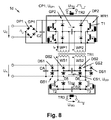
図8に、本発明の他の実施形態として、一次側及び二次側の電力スイッチ(T1〜T3)を直接駆動できるよう2個の制御変圧器TR2,TR3を追加した形態を示す。本実施形態では、対称的な制御信号を使用することで、変圧器TR2,TR3の二次巻線以外をトランジスタT1〜T3の制御入力端に接続する必要がないようにしている。 FIG. 8 shows another embodiment of the present invention in which two control transformers TR2 and TR3 are added so that the primary side and secondary side power switches (T1 to T3) can be directly driven. In this embodiment, by using symmetrical control signals, it is not necessary to connect other than the secondary windings of the transformers TR2 and TR3 to the control input terminals of the transistors T1 to T3.
輸送される電力は、一次インバータWR1内に対角配置されているトランジスタT1それぞれでのスイッチング周波数をfとした場合、概略
P=4・f・CP1・UE 2
で与えられる。このように、本変換器で輸送される電力Pは駆動周波数fに正比例する。制御変圧器TR2,TR3が低周波で飽和するのを防ぐため、パルス幅は相応の制限を受けている。
The transported power is approximately P = 4 · f · C P1 · U E 2 where f is the switching frequency in each of the transistors T1 diagonally arranged in the primary inverter WR1.
Given in. Thus, the electric power P transported by this converter is directly proportional to the drive frequency f. In order to prevent the control transformers TR2, TR3 from saturating at low frequencies, the pulse width is subject to corresponding limitations.
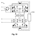
図19に、制御変圧器TR2,TR3を使用し一次インバータWR1内トランジスタT1やトランジスタT2,T3を制御するコントローラCTR2を、図8に示した電圧変換器1dに付加した構成を示す。
FIG. 19 shows a configuration in which a controller CTR2 for controlling the transistor T1 in the primary inverter WR1 and the transistors T2 and T3 using the control transformers TR2 and TR3 is added to the
図9に制御信号推移の好適例を示す。図示例では、一次インバータWR1や制御変圧器TR2,TR3のスイッチング周波数が入力周波数に比べ高くなっている。図示する都合上、ここではスイッチング周波数が実際よりかなり低めに描かれていることに留意されたい。また、明示されている通り、制御変圧器TR3の働きでトランジスタT2,T3が作動するのは入力電圧UEのゼロクロス域内、即ち次の式
|UE|<UA/u 又は |UE|<UA/(2u)
が成り立つ域内だけである。図10〜図12に、インバータWR1がパルス動作している期間に関し且つ三通りの動作条件に亘り、コンデンサCP1,CS1,CS2に加わる電圧UCP1,UCS1,UCS2や一次電流IPの典型的な推移例を示す。
FIG. 9 shows a preferred example of control signal transition. In the illustrated example, the switching frequency of the primary inverter WR1 and the control transformers TR2 and TR3 is higher than the input frequency. Note that for the sake of illustration, the switching frequency is depicted here much lower than it actually is. Further, as clearly indicated, the transistors T2 and T3 are activated by the action of the control transformer TR3 within the zero-cross range of the input voltage U E , that is, the following expression | U E | <U A / u or | U E | <U A / (2u)
It is only in the region where holds. 10 to 12 show typical examples of voltages U CP1 , U CS1 , U CS2 and primary current I P applied to the capacitors CP1, CS1, and CS2 with respect to a period during which the inverter WR1 operates in pulses and over three operating conditions. A typical transition example is shown.
図10に示したのは、入力電圧UEの過渡変動幅が出力電圧UAのそれに比べ狭い例である。この例では、電圧UEの過渡変動幅が60V、電圧UAのそれが160Vに設定されている。図示の通り、電流が減衰して0に達するより先に電圧UCP1の絶対値が60Vに達し第2一次フルブリッジ整流器GP2による制限を受けるため、コンデンサCP1,CS1は上下60Vの範囲内でしか充電されていない。他方、第2二次コンデンサCS2は−160Vから+160Vまでの範囲内で充電されている。これは、コンデンサCS2及びトランジスタT2,T3によに提供される昇圧変換機能が作動していることを表している。 FIG. 10 shows an example in which the transient fluctuation range of the input voltage U E is narrower than that of the output voltage U A. In this example, the transient fluctuation width of the voltage U E is set to 60V, and that of the voltage U A is set to 160V. As shown in the figure, since the absolute value of the voltage U CP1 reaches 60V and is limited by the second primary full-bridge rectifier GP2 before the current decays and reaches 0, the capacitors CP1 and CS1 are only within the range of 60V above and below The battery is not charged. On the other hand, the second secondary capacitor CS2 is charged within a range of −160V to + 160V. This indicates that the step-up conversion function provided by the capacitor CS2 and the transistors T2 and T3 is operating.
図11に示したのは、入力電圧UEの過渡変動幅が出力電圧UAのそれに比べやはり狭いけれども、図10に示した例に比べれば広い例である。この例では、電圧UEの公称的な過渡変動幅が120V、電圧UAのそれが160Vに設定されている。図示の通り、この例でも、第1一次コンデンサCP1の電圧過渡変動幅が第2一次整流器GP2による制限を受けているが、第1二次コンデンサCS1は120Vより若干広い過渡変動幅で充電されている。第2二次コンデンサCS2は、この例でも−160Vから+160Vまでの範囲内で充電されているが、その速度は図10に比べ有意に高まっている。即ち、コンデンサCS2及びトランジスタT2,T3により提供される昇圧変換機能がなおも作動している。 FIG. 11 shows an example in which the transient fluctuation range of the input voltage U E is narrower than that of the output voltage U A , but is wider than the example shown in FIG. In this example, the nominal transient fluctuation width of the voltage U E is set to 120V, and that of the voltage U A is set to 160V. As shown in the figure, in this example as well, the voltage transient fluctuation range of the first primary capacitor CP1 is limited by the second primary rectifier GP2, but the first secondary capacitor CS1 is charged with a transient fluctuation range slightly larger than 120V. Yes. The second secondary capacitor CS2 is charged in the range of −160V to + 160V in this example as well, but the speed is significantly higher than that in FIG. That is, the boost conversion function provided by the capacitor CS2 and the transistors T2 and T3 is still operating.
図12に示したのは、入力電圧UEの過渡変動幅が出力電圧UAのそれに比べ広い例である。この例では、電圧UEの公称的な過渡変動幅が180V、電圧UAのそれが160Vに設定されている。図示の通り、第1二次コンデンサCS1の電圧過渡変動幅が第2二次整流器GS2による160V制限を受ける一方、第1一次コンデンサCP1は180Vの過渡変動幅で充電されており、パルスの終わりに非常に近くなるまで第2一次整流器GP2による制限を受けていない。こうした場合、第2二次コンデンサCS2及びトランジスタT2,T3により提供される昇圧変換機能はもはや作動しない。 FIG. 12 shows an example in which the transient fluctuation range of the input voltage U E is wider than that of the output voltage U A. In this example, the nominal transient fluctuation width of the voltage U E is set to 180V, and that of the voltage U A is set to 160V. As shown in the figure, the voltage transient fluctuation range of the first secondary capacitor CS1 is limited by 160V by the second secondary rectifier GS2, while the first primary capacitor CP1 is charged with the transient fluctuation width of 180V, at the end of the pulse. Until very close, it is not limited by the second primary rectifier GP2. In such a case, the boost conversion function provided by the second secondary capacitor CS2 and the transistors T2 and T3 no longer operates.
更に、こうした変換器を例えば240V入力電圧仕様で設計し、より低い入力電圧例えば米国で使用される120Vで作動させた場合、出力電力はその「抵抗特性」によって有意に抑えられてしまう。入力電圧が半分であれば輸送される電力は1/4になる。この難点は、入力電圧が低いときにそれを倍加する単純な手段を設けることで克服することが可能である。 Furthermore, if such a converter is designed with a 240 V input voltage specification, for example, and operated at a lower input voltage, such as 120 V used in the United States, the output power is significantly suppressed by its “resistance characteristics”. If the input voltage is half, the transported power is ¼. This difficulty can be overcome by providing a simple means of doubling it when the input voltage is low.
図13に、本発明の他の実施形態として、そのセンタータップが第1一次整流器GP1の出力端に接続されている単巻変圧器TR4や、その変圧器TR4に備わるエンドタップの接続先を一次分巻巻線WP1,WP2及び第1一次コンデンサCP1からなる直列接続体と中間回路内正電位部位との間で随時切り替えるスイッチング素子S1,S2や、それらの素子S1,S2を駆動する巻線SP1を備える電圧変換器1eを示す。
FIG. 13 shows, as another embodiment of the present invention, a primary transformer TR4 whose center tap is connected to the output terminal of the first primary rectifier GP1, and a connection destination of an end tap provided in the transformer TR4. Switching elements S1 and S2 that are switched at any time between a series connection formed by the shunt windings WP1 and WP2 and the first primary capacitor CP1 and a positive potential portion in the intermediate circuit, and a winding SP1 that drives these elements S1 and S2 The
次に、この単巻変圧器TR4で追加された機能に関し、簡明化のため一次インバータWR1内トランジスタT1を省き対応する逆並列ボディダイオードDT1のみを示した図14を参照して説明する。この種のダイオードDT1は、対応するトランジスタT1で想定されているのとは逆の方向に電流が流れうるよう、同種のインバータで一般的なMOSFET、IGBT等に付設されるものである。同類のダイオードDT1が元々備わっていない場合でも、相応のダイオードを逆並列に外付けすることで、本実施形態のそれと同様の回路機能を実現することができる。 Next, the function added in the autotransformer TR4 will be described with reference to FIG. 14 showing only the corresponding antiparallel body diode DT1 without the transistor T1 in the primary inverter WR1 for the sake of simplicity. This kind of diode DT1 is attached to a general MOSFET, IGBT or the like with the same kind of inverter so that a current can flow in a direction opposite to that assumed in the corresponding transistor T1. Even when the similar diode DT1 is not originally provided, a circuit function similar to that of this embodiment can be realized by externally attaching a corresponding diode in antiparallel.
まず、トランジスタT1のうち左下のものがオンし、単巻変圧器TR4の左側分巻巻線に加わる電圧UTR4aが入力電圧UEに等しくなっているとする(UTR4a=UE)。また、単巻変圧器TR4の変圧比が1:2であるため(u=1:2)電圧分布が対称的で、右側分巻巻線に加わる電圧UTR4bが電圧UEに等しくなっているとする(UTR4b=UE)。無論、変圧比uをまた違う値にすることもできる。こうした電圧が加わると、トランジスタT1のうち右上のものに係る逆並列ボディダイオードDT1が導通するため、図中太線で示す電流経路に沿い、電圧UEの倍に当たる電圧が中間回路コンデンサCZに加わることとなる。従って、この電圧変換器1eでは、半分の電圧UEでも全電力を輸送し相応に大きな入力電流を流すことが可能である。ダイオードDT1が図14の如く元々備わっている場合は、このスイッチング動作を実行するための半導体素子を追加する必要もない。
First, it is assumed that the lower left transistor T1 is turned on and the voltage U TR4a applied to the left shunt winding of the autotransformer TR4 is equal to the input voltage U E (U TR4a = U E ). In addition, since the transformation ratio of the autotransformer TR4 is 1: 2 (u = 1: 2), the voltage distribution is symmetrical, and the voltage U TR4b applied to the right-hand side winding is equal to the voltage U E. (U TR4b = U E ). Of course, the transformation ratio u can be set to a different value. When such a voltage is applied, the anti-parallel body diode DT1 related to the transistor T1 on the upper right side is turned on, so that a voltage corresponding to twice the voltage U E is applied to the intermediate circuit capacitor CZ along the current path indicated by the thick line in the figure. It becomes. Therefore, in this
大電力が必要とされない場合は、単巻変圧器内分巻巻線の接続先を中間回路内正電位部位へと切り替える。この状態では、それら2個の分巻巻線が並列化され入力側フィルタチョークとして作動する。 When large electric power is not required, the connection destination of the shunt winding in the autotransformer is switched to the positive potential portion in the intermediate circuit. In this state, these two shunt windings are paralleled and operate as an input side filter choke.
図20に、図13に示した電圧変換器1eと類似するが絶縁変圧器TR5を備える点で異なる電圧変換器1gを示す。このように単巻変圧器TR4に代えて絶縁変圧器TR5を設け、その一次側を第1一次整流器GP1の出力端に接続する一方、二次側の接続先を一次分巻巻線WP1,WP2及び第1一次コンデンサCP1からなる直列接続体と中間回路内正電位部位との間でスイッチング素子により随時切り替えるようにした構成でも、同様の効果を得ることができる。
FIG. 20 shows a
図15に、図4に示した電圧変換器1bの変形例を示す。この変形例では、変圧器TR1として、漏れインダクタンス(図4では図示を省略)を利用できる磁界漏れ変圧器に代え、漏れインダクタンスの少ない密結合変圧器が使用されている。それに伴い、この図の変換器1bでは別個のチョークL1,L2が設けられ、図2に示したものに類する共振回路の形成が図られている。その意味では、この図の回路は図4に示した変換器1bの別表現、即ち磁界漏れ型の変圧器TR1に現る漏れインダクタンスを半分ずつチョークL1,L2で表した表現であるともいえる。
FIG. 15 shows a modification of the
図16に、図4に示した電圧変換器1bの二次側に別個のチョークL3,L4を設けた例を示す。その役目はお察しの通り図15中のチョークL1,L2と類似している。即ち、このチョークL3,L4は密結合型の変圧器TR1を補うためのものであると同時に、磁界漏れ変圧器の漏れインダクタンスを明示的に示したものであるともいえる。
FIG. 16 shows an example in which separate chokes L3 and L4 are provided on the secondary side of the
この図の例でチョークL3,L4が互いに結合されていることからわかるように、図15に示した例でチョークL1,L2を互いに結合させることも可能である。チョークL1・L2間結合やチョークL3・L4間結合は、例えば同一コアへの巻回という手段で、ひいてはかなり小型且つ単純な構成で実現することができる。 As can be seen from the fact that the chokes L3 and L4 are coupled to each other in the example of this figure, the chokes L1 and L2 can also be coupled to each other in the example shown in FIG. The coupling between the chokes L1 and L2 and the coupling between the chokes L3 and L4 can be realized, for example, by means of winding around the same core, and thus with a considerably small and simple configuration.
そして、図17に、本発明の他の実施形態として、図13に示した電圧変換器1eと同じく半分の入力電圧UEでも全電力を輸送可能な電圧変換器1fを示す。本実施形態では、単巻変圧器TR4を不要化するため、第2制御巻線SP2によって制御される第3スイッチS3の働きで第1一次コンデンサCP1に随時並列接続されるよう、補助第1一次コンデンサCP1’がコンデンサCP1に付設されている。同様に、第3制御巻線SP3によって制御される第4スイッチS4の働きで第1二次コンデンサCS1に随時並列接続されるよう、補助第1二次コンデンサCS1’がコンデンサCS1に付設されている。更に、第3制御巻線SP3によって制御される第5スイッチS5の働きで第2二次コンデンサCS2に随時並列接続されるよう、補助第2二次コンデンサCS2’がコンデンサCS2に付設されている。
FIG. 17 shows, as another embodiment of the present invention, a
スイッチS3〜S5を閉ざしたときにキャパシタンスが倍加されるので、入力電圧UEひいては電圧UCP1が半減しても、
P=IE・UE 及び P=4・f・CP1・UE 2
の関係により変圧器の一次分巻巻線WP1,WP2に流れる電流が同じ値に保たれる。なお、ここでいう周波数fは、中間回路コンデンサCZ、第1一次コンデンサCP1及び一次分巻巻線WP1,WP2で形成される発振回路の発振周波数ではなく、一次インバータWR1のスイッチング周波数のことである。
Since the capacitance is doubled when the switches S3 to S5 are closed, even if the input voltage U E and thus the voltage U CP1 are halved,
P = I E · U E and P = 4 · f · C P1 · U E 2
Therefore, the currents flowing through the primary shunt windings WP1 and WP2 of the transformer are maintained at the same value. The frequency f here is not the oscillation frequency of the oscillation circuit formed by the intermediate circuit capacitor CZ, the first primary capacitor CP1 and the primary shunt windings WP1 and WP2, but the switching frequency of the primary inverter WR1. .
また、第1一次コンデンサCP1に対する並列コンデンサ付設はスイッチングパルス継続時間の延長につながるが、図10〜図12に示した通り入力電圧UEの低下がスイッチングパルス継続時間の短縮につながるので、前者による延長分は後者による短縮分によって大なり小なり補償されることとなる。 Further, the provision of the parallel capacitor with respect to the first primary capacitor CP1 leads to the extension of the switching pulse duration. However, as shown in FIGS. 10 to 12, the decrease in the input voltage U E leads to the shortening of the switching pulse duration. The extension is compensated for more or less by the latter shortening.
図13に示した電圧変換器1eや図17に示した電圧変換器1fを使用すれば、同一の装置を、欧州における商用電圧と米国におけるそれとの違いによらず、同一の装置に給電することができる。その意味では、並列コンデンサ付設でキャパシタンスが倍加する構成が望ましいものの、補助的なコンデンサCP1’,CS1’,CS2’のキャパシタンス、厳密には対応するコンデンサに対するキャパシタンス比は、必要に応じ別の値に設定することも可能である。そして、留意すべきことに、スイッチS3〜S5を電気機械式のスイッチではなく固体スイッチにすることも可能である。
If the
総じて、上述した電圧変換器1a〜1fは本発明の多様な実施形態の例に過ぎず、本発明の適用範囲がそれらによって制限されるわけではないことに留意すべきである。例えば、上掲の諸実施形態で想定されているIGBTに代え他種トランジスタ、例えばMOSFETを使用することも可能である。特に、一次側共振回路は、それなりの長所を有するものの、本発明の機能を実現する上で必須のものではない。原則として、変圧器TR1向け交流電圧の生成には任意の手法を使用することができる。それによって二次側回路の機能が影響を受けることはない。本件技術分野で習熟を積まれた方々(いわゆる当業者)ならば、本発明の保護範囲から逸脱することなく、めいめいの需要に応じ本発明を適用することができよう。そして、図示した装置の諸部分が独立した発明の基礎にもなりうることをご理解頂きたい。
In general, it should be noted that the
1a〜1g 電圧変換器、CA フィルタコンデンサ、CP1 第1一次コンデンサ、CP1’ 補助第1一次コンデンサ、CS1 第1二次コンデンサ、CS1’ 補助第1二次コンデンサ、CS2 第2二次コンデンサ、CS2’ 補助第2二次コンデンサ、CTR1,CTR2 コントローラ、CZ 中間回路コンデンサ、D5,D6 ダイオード、DP1 GP1内ダイオード、DP2 GP2内ダイオード、DS1 GS1内ダイオード、DS2 GS2内ダイオード、DT1 WR1内ダイオード、GP1 第1一次整流器、GP2 第2一次整流器、GS1 第1二次整流器、GS2 第2二次整流器、I 電流、lE 入力電流、IP 一次電流、L1〜L4 チョーク、S1〜S5 スイッチ、SP1〜SP3 制御巻線、t 時刻、T1 WR1内トランジスタ、T2,T3 トランジスタ、TR1 変圧器、TR2 第1制御変圧器、TR3 第2制御変圧器、TR4 単巻変圧器、TR5 絶縁変圧器、U 電圧、UA 出力電圧、UCP1 CP1電圧、UCS1 CS1電圧、UCS2 CS2電圧、UCZ 中間回路電圧、UE 入力電圧、u 変圧比、UTR2 TR2電圧、UTR3 TR3電圧、UTR4a TR4内左側分巻巻線電圧、UTR4b TR4内右側分巻巻線電圧、UWP1 WP1電圧、UWP2 WP2電圧、UWS1 WS1電圧、UWS2 WS2電圧、WP1,WP2 TR1内一次分巻巻線、WR1 インバータ、WS1,WS2 TR1内二次分巻巻線。 1a to 1g Voltage converter, CA filter capacitor, CP1 first primary capacitor, CP1 ′ auxiliary first primary capacitor, CS1 first secondary capacitor, CS1 ′ auxiliary first secondary capacitor, CS2 second secondary capacitor, CS2 ′ Auxiliary second secondary capacitor, CTR1, CTR2 controller, CZ intermediate circuit capacitor, D5, D6 diode, DP1 GP1 diode, DP2 GP2 diode, DS1 GS1 diode, DS2 GS2 diode, DT1 WR1 diode, GP1 first primary rectifier, GP2 second primary rectifier, GS1 first secondary rectifier, GS2 second secondary rectifier, I the current, l E input current, I P primary current, L1 to L4 chalk, S1-S5 switch, SP1 to SP3 control Winding, t time, transistor in T1 WR1, T2, T3 transistors, TR1 transformer, TR2 first control transformer, TR3 second control transformer, TR4 autotransformer, TR5 isolation transformer, U voltage, U A output voltage, U CP1 CP1 voltage, U CS1 CS1 voltage, U CS2 CS2 voltage, U CZ intermediate circuit voltage, U E input voltage, u transformation ratio, U TR2 TR2 voltage, U TR3 TR3 voltage, U TR4a TR4 left side winding voltage, U TR4b TR4 right side winding Voltage, U WP1 WP1 voltage, U WP2 WP2 voltage, U WS1 WS1 voltage, U WS2 WS2 voltage, WP1, WP2 TR1 primary shunt winding, WR1 inverter, WS1, WS2 TR1 secondary shunt winding.
Claims (38)
入力交流電圧(UE)より周波数が高い交流電圧をその入力交流電圧(UE)に応じ変圧器の一次巻線(WP1,WP2)上に発生させる手段と、
を備え、入力電圧(UE)を出力直流電圧(UA)に変換する電圧変換器(1a〜1g)であって、
その入力端を介し変圧器(TR1)内の対応する二次分巻巻線(WS1,WS2)の第1端に接続されており、出力端が出力直流電圧(UA)の供給に使用されるフルブリッジ型の第1二次整流器(GS1)と、
第1二次整流器(GS1)の入力端同士を結ぶ直列接続体が二次分巻巻線(WS1,WS2)との協働で形成されるよう二次分巻巻線(WS1,WS2)の第2端間に挿入された第1二次コンデンサ(CS1)と、
その入力端に第1二次コンデンサ(CS1)及び各二次分巻巻線(WS1,WS2)の第2端が接続される一方、その出力が第1二次整流器(GS1)のそれと同極性になるよう、第1二次整流器(GS1)に並列接続されたフルブリッジ型の第2二次整流器(GS2)と、
を備えることを特徴とする電圧変換器。 A transformer (TR1) having one or more primary windings (WP1, WP2) and a plurality of secondary shunt windings (WS1, WS2);
Means for generating on the input AC voltage transformer primary winding according to (U E) from the high frequency AC voltage that the input AC voltage (U E) (WP1, WP2 ),
A voltage converter (1a to 1g) for converting an input voltage (U E ) into an output DC voltage (U A ),
The input end is connected to the first end of the corresponding secondary shunt winding (WS1, WS2) in the transformer (TR1), and the output end is used to supply the output DC voltage (U A ). A full bridge type first secondary rectifier (GS1),
The secondary shunt winding (WS1, WS2) is formed so that a series connection body connecting the input ends of the first secondary rectifier (GS1) is formed in cooperation with the secondary shunt winding (WS1, WS2). A first secondary capacitor (CS1) inserted between the second ends;
The first secondary capacitor (CS1) and the second ends of the secondary shunt windings (WS1, WS2) are connected to the input terminals of the first secondary capacitor (CS1), and the output is the same polarity as that of the first secondary rectifier (GS1). A full bridge type second secondary rectifier (GS2) connected in parallel to the first secondary rectifier (GS1),
A voltage converter comprising:
上掲の変圧器(TR1)に備わる一次巻線の個数が2個(WP1,WP2)であり、
それら一次巻線(WP1,WP2)上に交流電圧を発生させる手段が、
入力交流電圧(UE)を整流するフルブリッジ型又はセンターポイント型の第1一次整流器(GP1)と、
その出力端を介し変圧器(TR1)内の対応する一次分巻巻線(WP1,WP2)に接続されたフルブリッジ型の一次インバータ(WR1)と、
一次インバータ(WR1)の出力端間を結ぶ直列接続体が一次巻線(WP1,WP2)との協働で形成されるよう一次巻線(WP1,WP2)間に挿入された第1一次コンデンサ(CP1)と、
その入力端を介し第1一次コンデンサ(CP1)、出力端を介し一次インバータ(WR1)の入力端に接続されており、一次インバータ(WR1)に対し逆並列なフルブリッジ型の第2一次整流器(GP2)と、
を有することを特徴とする電圧変換器。 The voltage converter (1a-1g) according to claim 1,
The number of primary windings provided in the above transformer (TR1) is two (WP1, WP2),
Means for generating an alternating voltage on the primary windings (WP1, WP2),
A full bridge type or center point type first primary rectifier (GP1) for rectifying an input AC voltage (U E );
A full-bridge primary inverter (WR1) connected to a corresponding primary shunt winding (WP1, WP2) in the transformer (TR1) via its output end;
A first primary capacitor inserted between the primary windings (WP1, WP2) so that a series connection body connecting the output terminals of the primary inverter (WR1) is formed in cooperation with the primary windings (WP1, WP2). CP1)
The first primary capacitor (CP1) is connected through the input terminal, and is connected to the input terminal of the primary inverter (WR1) through the output terminal, and is a full bridge type second primary rectifier (in reverse parallel to the primary inverter (WR1)). GP2),
The voltage converter characterized by having.
入力交流電流をより高周波の交流電流に変換して変圧器の一次巻線に供給するAC/AC変換回路と、
その第1入力端を介し第1二次分巻巻線の第1端、第2入力端を介し第2二次分巻巻線の第1端に接続されており、出力端が出力直流電圧の供給に使用されるフルブリッジ型の第1二次整流器と、
その第1端を介し第1二次分巻巻線の第2端、第2端を介し第2二次分巻巻線の第2端に接続された第1二次コンデンサと、
その第1入力端を介し第1二次分巻巻線の第2端及び第1二次コンデンサの第1端、第2入力端を介し第2二次分巻巻線の第2端及び第1二次コンデンサの第2端に接続されており、出力端に第1二次整流器のそれと同極性の出力が現れるフルブリッジ型の第2二次整流器と、
を備える電圧変換器。 A transformer having one or more primary windings and first and second secondary shunt windings, the windings having respective first and second ends;
An AC / AC conversion circuit that converts an input AC current into a higher frequency AC current and supplies it to the primary winding of the transformer;
The first input terminal is connected to the first end of the first secondary shunt winding, the second input terminal is connected to the first end of the second secondary shunt winding, and the output terminal is connected to the output DC voltage. A first full-bridge rectifier used to supply
A first secondary capacitor connected to the second end of the first secondary shunt winding via the first end, the second end of the second secondary shunt winding via the second end;
The second end of the first secondary shunt winding and the first end of the first secondary capacitor via the first input end, the second end of the second secondary shunt winding and the second end of the first secondary capacitor via the second input end. A full-bridge type second secondary rectifier connected to the second end of the first secondary capacitor and having an output of the same polarity as that of the first secondary rectifier at the output end;
A voltage converter comprising:
その第1端を介し第1二次整流器の第1入力端、第2端を介し第1二次整流器の第2入力端に接続された第2二次コンデンサと、
第2二次コンデンサに直列接続されたスイッチと、
を備える電圧変換器。 The voltage converter of claim 14 , further comprising:
A second secondary capacitor connected to the first input terminal of the first secondary rectifier through the first terminal and the second input terminal of the first secondary rectifier through the second terminal;
A switch connected in series with the second secondary capacitor;
A voltage converter comprising:
上掲のスイッチたる第1トランジスタと、
第1トランジスタに逆並列接続された第1ダイオードと、
を備える電圧変換器。 The voltage converter of claim 15 , further comprising:
A first transistor as a switch,
A first diode connected in antiparallel to the first transistor;
A voltage converter comprising:
第2二次コンデンサの第2端に接続された第2トランジスタと、
第2トランジスタに逆並列接続された第2ダイオードと、
を備え、第1トランジスタ、第2二次コンデンサ及び第2トランジスタを有する直列接続体に沿い第1・第2トランジスタ間で順バイアス方向が異なる電圧変換器。 The voltage converter of claim 16 , further comprising:
A second transistor connected to the second end of the second secondary capacitor;
A second diode connected in antiparallel to the second transistor;
A voltage converter having a forward bias direction different between the first and second transistors along a series connection having a first transistor, a second secondary capacitor, and a second transistor.
その第1端を介し第1二次整流器の第1入力端、第2端を介し第1二次整流器の第2入力端に接続された第2二次コンデンサと、
第2二次コンデンサに直列接続されたスイッチと、
第2二次コンデンサに対し並列になるよう第1二次整流器の第1端・第2端間に随時挿入される補助第2二次コンデンサと、
を備える電圧変換器。 The voltage converter of claim 22 , further comprising:
A second secondary capacitor connected to the first input terminal of the first secondary rectifier through the first terminal and the second input terminal of the first secondary rectifier through the second terminal;
A switch connected in series with the second secondary capacitor;
An auxiliary second secondary capacitor inserted as needed between the first and second ends of the first secondary rectifier so as to be in parallel with the second secondary capacitor;
A voltage converter comprising:
上記スイッチとして第2二次コンデンサの第1端に接続された第1トランジスタと、
第2二次コンデンサの第2端に接続された第2トランジスタと、
を備え、第1トランジスタ、第2二次コンデンサ及びそれと並列な補助第2二次コンデンサ、並びに第2トランジスタを有する直列接続体に沿い第1・第2トランジスタ間で順バイアス方向が異なる電圧変換器。 The voltage converter of claim 23 , further comprising:
A first transistor connected to the first end of the second secondary capacitor as the switch;
A second transistor connected to the second end of the second secondary capacitor;
And a voltage converter having a forward bias direction different between the first and second transistors along a series connection having the first transistor, the second secondary capacitor and the auxiliary second secondary capacitor in parallel therewith, and the second transistor .
入力交流電流を整流する第1一次整流器と、
その第1出力端を介し第1一次分巻巻線の第1端、第2出力端を介し第2一次分巻巻線の第1端に接続されており、入力端が第1一次整流器からの整流済電流受入に使用されるフルブリッジ型の一次インバータと、
その第1入力端を介し第1一次分巻巻線の第2端、第2入力端を介し第2一次分巻巻線の第2端、出力端を介し一次インバータの入力端に接続された第2一次整流器と、
その第1端を介し第1一次分巻巻線の第2端及び第2一次整流器の第1入力端、第2端を介し第2一次分巻巻線の第2端及び第2一次整流器の第2入力端に接続された第1一次コンデンサと、
その第1入力端を介し第1二次分巻巻線の第1端、第2入力端を介し第2二次分巻巻線の第1端に接続されており、出力端が出力直流電圧の供給に使用されるフルブリッジ型の第1二次整流器と、
その第1端を介し第2二次分巻巻線の第1端、第2端を介し第2二次分巻巻線の第2端に接続された第1二次コンデンサと、
その第1入力端を介し第1二次分巻巻線の第2端及び第1二次コンデンサの第1端、第2入力端を介し第2二次分巻巻線の第2端及び第1二次コンデンサの第2端に接続されており、出力端に第1二次整流器のそれと同極性の出力が現れるフルブリッジ型の第2二次整流器と、
を備える電圧変換器。 Transformer having first and second primary shunt windings on the primary side, and first and second secondary shunt windings on the secondary side, each of which has first and second ends. And
A first primary rectifier for rectifying an input alternating current;
The first output terminal is connected to the first end of the first primary shunt winding, the second output terminal is connected to the first end of the second primary shunt winding, and the input terminal is connected to the first primary rectifier. A full-bridge primary inverter used for receiving the rectified current of
The first input terminal is connected to the second end of the first primary winding, the second input terminal is connected to the second end of the second primary winding and the output terminal is connected to the input terminal of the primary inverter A second primary rectifier;
The second end of the first primary shunt winding and the first input end of the second primary rectifier through the first end, the second end of the second primary shunt winding and the second end of the second primary rectifier through the second end. A first primary capacitor connected to the second input;
The first input terminal is connected to the first end of the first secondary shunt winding, the second input terminal is connected to the first end of the second secondary shunt winding, and the output terminal is connected to the output DC voltage. A first full-bridge rectifier used to supply
A first secondary capacitor connected to the first end of the second secondary shunt winding via the first end, and to the second end of the second secondary shunt winding via the second end;
The second end of the first secondary shunt winding and the first end of the first secondary capacitor via the first input end, the second end of the second secondary shunt winding and the second end of the first secondary capacitor via the second input end. A full-bridge type second secondary rectifier connected to the second end of the first secondary capacitor and having an output of the same polarity as that of the first secondary rectifier at the output end;
A voltage converter comprising:
その第1端を介し第1二次整流器の第1入力端、第2端を介し第1二次整流器の第2入力端に接続された第2二次コンデンサと、
第2二次コンデンサに直列接続されておりその第2二次コンデンサの第1端に接続された第1トランジスタを有するスイッチと、
第2二次コンデンサの第2端に接続された第2トランジスタと、
第1及び第2トランジスタを可制御的に駆動する第2制御変圧器と、
を備える電圧変換器。 The voltage converter of claim 26 , further comprising:
A second secondary capacitor connected to the first input terminal of the first secondary rectifier through the first terminal and the second input terminal of the first secondary rectifier through the second terminal;
A switch having a first transistor connected in series to a second secondary capacitor and connected to a first end of the second secondary capacitor;
A second transistor connected to the second end of the second secondary capacitor;
A second control transformer for controllably driving the first and second transistors;
A voltage converter comprising:
そのセンタータップが第1一次整流器の出力端に接続されており、且つ第1及び第2エンドタップを有する単巻変圧器と、
単巻変圧器の第1エンドタップを第1一次分巻巻線の第1端、第2エンドタップを第2一次分巻巻線の第1端に可制御的に接続させる1個又は複数個の単巻変圧器制御スイッチと、
を備える電圧変換器。 28. The voltage converter of claim 27 , further comprising:
A self-winding transformer having a center tap connected to the output end of the first primary rectifier and having first and second end taps;
One or more controllably connecting the first end tap of the autotransformer to the first end of the first primary winding and the second end tap to the first end of the second primary winding. With auto-transformer control switch,
A voltage converter comprising:
一次側及び二次側のうち一次側に第1一次整流器の出力端が接続された絶縁変圧器と、
絶縁変圧器の二次側を第1及び第2一次分巻巻線の第1端に可制御的に接続させる1個又は複数個の絶縁変圧器制御スイッチと、
を備える電圧変換器。 28. The voltage converter of claim 27 , further comprising:
An isolation transformer in which the output terminal of the first primary rectifier is connected to the primary side of the primary side and the secondary side;
One or more isolation transformer control switches that controllably connect the secondary side of the isolation transformer to the first ends of the first and second primary shunt windings;
A voltage converter comprising:
そのセンタータップが第1一次整流器の出力端に接続されており、且つ第1及び第2エンドタップを有する単巻変圧器と、
単巻変圧器の第1エンドタップを第1一次分巻巻線の第1端、第2エンドタップを第2一次分巻巻線の第1端に可制御的に接続させる1個又は複数個の単巻変圧器制御スイッチと、
を備える電圧変換器。 The voltage converter of claim 25 , further comprising:
A self-winding transformer having a center tap connected to the output end of the first primary rectifier and having first and second end taps;
One or more controllably connecting the first end tap of the autotransformer to the first end of the first primary winding and the second end tap to the first end of the second primary winding. With auto-transformer control switch,
A voltage converter comprising:
一次側及び二次側のうち一次側に第1一次整流器の出力端が接続された絶縁変圧器と、
絶縁変圧器の二次側を第1及び第2一次分巻巻線の第1端に可制御的に接続させる1個又は複数個の絶縁変圧器制御スイッチと、
を備える電圧変換器。 The voltage converter of claim 25 , further comprising:
An isolation transformer in which the output terminal of the first primary rectifier is connected to the primary side of the primary side and the secondary side;
One or more isolation transformer control switches that controllably connect the secondary side of the isolation transformer to the first ends of the first and second primary shunt windings;
A voltage converter comprising:
第1又は第2一次分巻巻線に直列接続された1個又は複数個の補助チョークを備え、
上掲の変圧器が密結合型である電圧変換器。 The voltage converter of claim 32 , further comprising:
One or more auxiliary chokes connected in series to the first or second primary shunt winding;
A voltage converter in which the above transformer is a tightly coupled type.
その第1端を介し第1二次整流器の第1入力端、第2端を介し第1二次整流器の第2入力端に接続された第2二次コンデンサと、
第2二次コンデンサに直列接続されたスイッチと、
第2二次コンデンサに対し並列になるよう第1二次整流器の第1入力端・第2入力端間に随時挿入される補助第2二次コンデンサと、
を備える電圧変換器。 The voltage converter of claim 36 , further comprising:
A second secondary capacitor connected to the first input terminal of the first secondary rectifier through the first terminal and the second input terminal of the first secondary rectifier through the second terminal;
A switch connected in series with the second secondary capacitor;
An auxiliary second secondary capacitor inserted as needed between the first input terminal and the second input terminal of the first secondary rectifier so as to be in parallel with the second secondary capacitor;
A voltage converter comprising:
入力交流電流を整流する第1一次整流器と、
その第1出力端を介し第1一次分巻巻線の第1端、第2出力端を介し第2一次分巻巻線の第1端に接続されており、入力端が第1一次整流器からの整流済電流受入に使用されるフルブリッジ型の一次インバータと、
その第1入力端を介し第1一次分巻巻線の第2端、第2入力端を介し第2一次分巻巻線の第2端、出力端を介し一次インバータの入力端に接続された第2一次整流器と、
その第1端を介し第1一次分巻巻線の第2端及び第2一次整流器の第1入力端、第2端を介し第2一次分巻巻線の第2端及び第2一次整流器の第2入力端に接続された第1一次コンデンサと、
その第1入力端を介し第1二次分巻巻線の第1端、第2入力端を介し第2二次分巻巻線の第1端に接続されており、出力端が出力直流電圧の供給に使用されるフルブリッジ型の第1二次整流器と、
その第1端を介し第1二次整流器の第1入力端、第2端を介し第1二次整流器の第2入力端に接続された第2二次コンデンサと、
第2二次コンデンサに直列接続されており第1トランジスタを有するスイッチと、
第1トランジスタに逆並列接続された第1ダイオードと、
第2二次コンデンサの第2端に接続された第2トランジスタと、
第2トランジスタに逆並列接続された第2ダイオードと、
を備え、第1トランジスタ、第2二次コンデンサ及び第2トランジスタを有する直列接続体に沿い第1及び第2トランジスタ間で順バイアス方向が異なる電圧変換器。 Transformer having first and second primary shunt windings on the primary side, and first and second secondary shunt windings on the secondary side, each of which has first and second ends. And
A first primary rectifier for rectifying an input alternating current;
The first output terminal is connected to the first end of the first primary shunt winding, the second output terminal is connected to the first end of the second primary shunt winding, and the input terminal is connected to the first primary rectifier. A full-bridge primary inverter used for receiving the rectified current of
The first input terminal is connected to the second end of the first primary shunt winding, the second input terminal is connected to the second end of the second primary shunt winding, and the output terminal is connected to the input terminal of the primary inverter. A second primary rectifier;
The second end of the first primary shunt winding and the first input end of the second primary rectifier through the first end, the second end of the second primary shunt winding and the second end of the second primary rectifier through the second end. A first primary capacitor connected to the second input;
The first input terminal is connected to the first end of the first secondary shunt winding, the second input terminal is connected to the first end of the second secondary shunt winding, and the output terminal is connected to the output DC voltage. A first full-bridge rectifier used to supply
Its first secondary rectifier first input terminal of via a first end, a second secondary capacitor connected to the second input terminal of the first secondary rectifier via the second end,
A switch having a first transistor connected in series to a second secondary capacitor;
A first diode connected in antiparallel to the first transistor;
A second transistor connected to the second end of the second secondary capacitor;
A second diode connected in antiparallel to the second transistor;
The provided, the first transistor, the voltage converter is a forward bias differs between the first and second transistors along series connection with a second secondary capacitor and the second transistor.
Applications Claiming Priority (5)
| Application Number | Priority Date | Filing Date | Title |
|---|---|---|---|
| US35979310P | 2010-06-29 | 2010-06-29 | |
| EP10167766 | 2010-06-29 | ||
| EP10167766.4 | 2010-06-29 | ||
| US61/359,793 | 2010-06-29 | ||
| PCT/IB2011/052841 WO2012001627A2 (en) | 2010-06-29 | 2011-06-28 | Voltage converter |
Publications (2)
| Publication Number | Publication Date |
|---|---|
| JP2013530673A JP2013530673A (en) | 2013-07-25 |
| JP5851501B2 true JP5851501B2 (en) | 2016-02-03 |
Family
ID=43244903
Family Applications (1)
| Application Number | Title | Priority Date | Filing Date |
|---|---|---|---|
| JP2013517629A Active JP5851501B2 (en) | 2010-06-29 | 2011-06-28 | Voltage converter |
Country Status (6)
| Country | Link |
|---|---|
| US (1) | US8693214B2 (en) |
| EP (1) | EP2589136B1 (en) |
| JP (1) | JP5851501B2 (en) |
| KR (1) | KR20130126580A (en) |
| CN (1) | CN102959840B (en) |
| WO (1) | WO2012001627A2 (en) |
Families Citing this family (12)
| Publication number | Priority date | Publication date | Assignee | Title |
|---|---|---|---|---|
| EP2385617A1 (en) * | 2010-05-06 | 2011-11-09 | Brusa Elektronik AG | Dc/dc converter with control |
| US9641095B1 (en) * | 2014-02-21 | 2017-05-02 | Pai Capital Llc | Power converter output stage using heat dissipating bus bars |
| EP3024133A1 (en) * | 2014-11-24 | 2016-05-25 | Broadband Power Solutions | DC-to-AC power converter |
| US20160226367A1 (en) * | 2015-02-03 | 2016-08-04 | Alstom Technology Ltd | High power electrical module and high power electrical circuit |
| US9812977B2 (en) * | 2015-04-01 | 2017-11-07 | Futurewei Technologies, Inc. | Resonant converters with an improved voltage regulation range |
| AU2016377688B2 (en) * | 2015-12-22 | 2022-03-10 | Thermatool Corp. | High frequency power supply system with closely regulated output for heating a workpiece |
| JP6745134B2 (en) * | 2016-05-12 | 2020-08-26 | 東京エレクトロン株式会社 | Plasma processing device |
| US10944283B2 (en) | 2017-12-22 | 2021-03-09 | Industrial Technology Research Institute | Distributed single-stage on-board charging device and method thereof |
| DE102019123554A1 (en) | 2018-09-03 | 2020-03-05 | Brusa Elektronik Ag | Converter device |
| CN109286325B (en) * | 2018-11-14 | 2020-08-14 | 广东电网有限责任公司 | Resonance analysis method for multi-machine parallel connection of power electronic transformer |
| DE102019106485B4 (en) * | 2019-03-14 | 2021-04-08 | Dr. Ing. H.C. F. Porsche Aktiengesellschaft | Weissach rectifier arrangement |
| US11081968B2 (en) * | 2019-06-12 | 2021-08-03 | Delta Electronics, Inc. | Isolated boost converter |
Family Cites Families (65)
| Publication number | Priority date | Publication date | Assignee | Title |
|---|---|---|---|---|
| DE1638344A1 (en) | 1968-03-05 | 1969-09-18 | Kaick Avk Generatoren | Brushless synchronous machine with special exciter |
| US3517300A (en) | 1968-04-16 | 1970-06-23 | Gen Electric | Power converter circuits having a high frequency link |
| DE1763299A1 (en) | 1968-05-02 | 1971-10-21 | Licentia Gmbh | De-excitation circuit for brushless synchronous machines excited by rotating diodes |
| DE2127497A1 (en) | 1971-05-28 | 1972-12-07 | Siemens Ag | Arrangement for the quick de-excitation of brushless synchronous machines, which are excited by rotating uncontrolled rectifiers |
| US4017784A (en) * | 1976-05-17 | 1977-04-12 | Litton Systems, Inc. | DC to DC converter |
| DE2624532B2 (en) | 1976-06-01 | 1979-10-11 | Siemens Ag, 1000 Berlin Und 8000 Muenchen | Circuit arrangement for connecting an electronic device to an alternating voltage network |
| CA1097738A (en) | 1976-08-20 | 1981-03-17 | Westinghouse Electric Corporation | Fast de-excitation brushless exciter |
| US4336486A (en) | 1980-01-09 | 1982-06-22 | Westinghouse Electric Corp. | Dynamoelectric machines brushless supplemental excitation system |
| DE3305224A1 (en) | 1983-02-16 | 1984-08-16 | Bbc Brown Boveri & Cie | ON-BOARD BATTERY CHARGER |
| GB2152770B (en) | 1983-11-15 | 1987-04-29 | Yokogawa Hokushin Electric | Dc/dc converter |
| DE3406274A1 (en) | 1984-02-17 | 1985-08-29 | Siemens AG, 1000 Berlin und 8000 München | ELECTRIC SYNCHRONOUS MACHINE TO BE EXCITED BY ROTATING RECTIFIERS |
| SE452451B (en) | 1984-06-07 | 1987-11-30 | Svenska Utvecklings Ab | MEMBRANE STILLATION DEVICE |
| US4695933A (en) | 1985-02-11 | 1987-09-22 | Sundstrand Corporation | Multiphase DC-DC series-resonant converter |
| CA2054319C (en) | 1991-06-28 | 1995-01-17 | Hirokazu Ioroi | Power supply unit for arc processing |
| SE500682C2 (en) | 1992-04-02 | 1994-08-08 | Asea Brown Boveri | Method and apparatus for demagnetizing brushless synchronous generators |
| AT403422B (en) | 1993-06-18 | 1998-02-25 | Steyr Daimler Puch Ag | CONTROL CIRCUIT FOR BATTERY-POWERED VEHICLES |
| US5555494A (en) | 1993-09-13 | 1996-09-10 | Morris; George Q. | Magnetically integrated full wave DC to DC converter |
| US5438498A (en) * | 1993-12-21 | 1995-08-01 | Raytheon Company | Series resonant converter having a resonant snubber |
| DE9403447U1 (en) | 1994-03-01 | 1994-04-28 | Siemens Ag | Power supply device for passenger coaches |
| JPH0865904A (en) | 1994-06-06 | 1996-03-08 | Nippondenso Co Ltd | Charger for electric automobile |
| JP2865194B2 (en) | 1994-07-29 | 1999-03-08 | 株式会社アイ・ヒッツ研究所 | Single-phase input three-phase full-wave rectifier circuit and single-phase input pseudo four-phase full-wave rectifier circuit |
| US5710698A (en) | 1994-09-30 | 1998-01-20 | Lockheed Martin Energy Systems, Inc. | Delta connected resonant snubber circuit |
| AT405227B (en) | 1995-12-11 | 1999-06-25 | Steyr Daimler Puch Ag | CHARGING DEVICE FOR A BATTERY-POWERED VEHICLE |
| DE19546420C1 (en) | 1995-12-12 | 1997-04-10 | Siemens Ag | Static fail-safe current supply device for variable speed drive |
| US5754413A (en) | 1996-02-23 | 1998-05-19 | Lucent Technologies Inc. | Reduced voltage stress asymmetrical DC-to-DC converter using first and second transformers having differing turns ratios |
| US5973939A (en) | 1996-08-29 | 1999-10-26 | Trw Inc. | Double forward converter with soft-PWM switching |
| SE520786C2 (en) | 1997-03-24 | 2003-08-26 | Abb Ab | Electric power transmission system |
| DE19836401A1 (en) | 1997-09-19 | 2000-02-17 | Salcomp Oy Salo | Device for charging accumulators |
| DE19750041C1 (en) | 1997-11-12 | 1999-01-21 | Sma Regelsysteme Gmbh | Semiconductor DC voltage regulator |
| JP3361047B2 (en) | 1998-01-30 | 2003-01-07 | 株式会社東芝 | Power supply for vehicles |
| DE19941170A1 (en) | 1999-08-30 | 2001-03-08 | Herbert Weh | Self-symmetrising supply system has semiconducting switches in sub-converters that are loaded voltage symmetrically without active regulation or additional circuitry |
| US6169683B1 (en) | 1999-10-07 | 2001-01-02 | Ericsson Inc. | Resonant gate drive for synchronous rectifiers |
| US6337801B2 (en) | 1999-12-16 | 2002-01-08 | Virginia Tech Intellectual Properties, Inc. | Three-phase zero-current-transition (ZCT) inverters and rectifiers with three auxiliary switches |
| US7187566B2 (en) | 2000-03-17 | 2007-03-06 | Daikin Industries, Ltd. | Three-phase rectifier |
| JP4392975B2 (en) * | 2000-09-28 | 2010-01-06 | 新電元工業株式会社 | Constant power output DC power supply |
| DE10051156B4 (en) | 2000-10-16 | 2005-09-22 | Siemens Ag | Method and converter circuit for medium-frequency transformatory energy transmission |
| US6490183B2 (en) | 2000-12-29 | 2002-12-03 | Ericsson, Inc. | Method and apparatus for minimizing negative current build up in DC-DC converters with synchronous rectification |
| JP3463807B2 (en) | 2001-01-24 | 2003-11-05 | 日新電機株式会社 | DC-DC converter |
| JP3555137B2 (en) | 2001-10-01 | 2004-08-18 | 日新電機株式会社 | Bidirectional DC-DC converter |
| CA2369060C (en) | 2001-01-24 | 2005-10-04 | Nissin Electric Co., Ltd. | Dc-dc-converter and bi-directional dc-dc converter and method of controlling the same |
| DE10126256A1 (en) * | 2001-05-29 | 2002-12-05 | Philips Corp Intellectual Pty | Power system |
| DE10151153A1 (en) | 2001-10-19 | 2003-04-30 | Bombardier Transp Gmbh | Device for charging batteries for electric vehicles has converter containing inverter for producing a.c. voltage from step-up device's D.C. output and rectifier coupled via transformer |
| US6603675B1 (en) | 2002-01-17 | 2003-08-05 | Abb Ab | Apparatus and a method for voltage conversion |
| DE10217889A1 (en) | 2002-04-22 | 2003-11-13 | Siemens Ag | Power supply with a direct converter |
| US6765810B2 (en) | 2002-08-02 | 2004-07-20 | Artesyn Technologies, Inc. | Full-wave coupled inductor power converter having synchronous rectifiers and two input switches that are simultaneously off for a time period of each switching cycle |
| JP2004088814A (en) | 2002-08-22 | 2004-03-18 | Nissin Electric Co Ltd | Dc-dc converter |
| JP2005006455A (en) | 2003-06-13 | 2005-01-06 | Toshiba Corp | Rectification device |
| JP3931858B2 (en) * | 2003-07-29 | 2007-06-20 | 松下電器産業株式会社 | Power supply |
| US7149096B2 (en) | 2004-02-18 | 2006-12-12 | Astec International Limited | Power converter with interleaved topology |
| GB2421365B (en) | 2004-12-16 | 2007-12-27 | Alstom | Matrix converters |
| DE102005023290A1 (en) | 2005-05-20 | 2006-11-23 | Sma Technologie Ag | Bidirectional battery inverter |
| DE102005036806A1 (en) | 2005-08-02 | 2007-02-08 | Lorch Schweißtechnik GmbH | Electric power source, in particular welding power source |
| JP4628426B2 (en) | 2005-09-15 | 2011-02-09 | 三菱電機株式会社 | Control device for vehicle alternator |
| WO2007060506A2 (en) | 2005-10-14 | 2007-05-31 | Astec International Limited | Multiphase dc to dc converter |
| DE102006025975B4 (en) * | 2006-06-02 | 2008-08-28 | Siemens Ag Österreich | Inverter circuit and method for operating the inverter circuit |
| DE102006055126A1 (en) | 2006-11-22 | 2008-06-05 | Siemens Ag | Input voltage or input direct current voltage conversion method for use in power supply device i.e. current fed clock converter, involves decoupling induction voltage that is automatically induced in load coil as further output voltage |
| FI121643B (en) | 2007-03-16 | 2011-02-15 | Vacon Oyj | Current harmonics limitation |
| US7679941B2 (en) | 2007-06-06 | 2010-03-16 | General Electric Company | Power conversion system with galvanically isolated high frequency link |
| JP4770798B2 (en) | 2007-06-15 | 2011-09-14 | 株式会社豊田自動織機 | Power supply |
| JP4995277B2 (en) * | 2007-06-28 | 2012-08-08 | 新電元工業株式会社 | Bidirectional DC / DC converter |
| US7768800B2 (en) * | 2007-12-12 | 2010-08-03 | The Board Of Trustees Of The University Of Illinois | Multiphase converter apparatus and method |
| EP2144359A2 (en) | 2008-07-09 | 2010-01-13 | SMA Solar Technology AG | DC/DC-converter |
| KR20110110783A (en) | 2009-01-29 | 2011-10-07 | 브루사 일렉트로닉 아게 | Converter for single-phase and three-phase operation, d.c. voltage supply and battery charger |
| KR20120048572A (en) | 2009-06-24 | 2012-05-15 | 브루사 일렉트로닉 아게 | Circuit arrangement for power distribution in a motor vehicle |
| US8411473B2 (en) * | 2010-12-20 | 2013-04-02 | Allis Electric Co., Ltd. | Three-phase power supply with three-phase three-level DC/DC converter |
-
2011
- 2011-06-28 EP EP11738318.2A patent/EP2589136B1/en active Active
- 2011-06-28 US US13/700,800 patent/US8693214B2/en active Active
- 2011-06-28 CN CN201180032382.0A patent/CN102959840B/en active Active
- 2011-06-28 JP JP2013517629A patent/JP5851501B2/en active Active
- 2011-06-28 KR KR1020137002192A patent/KR20130126580A/en not_active Application Discontinuation
- 2011-06-28 WO PCT/IB2011/052841 patent/WO2012001627A2/en active Application Filing
Also Published As
| Publication number | Publication date |
|---|---|
| JP2013530673A (en) | 2013-07-25 |
| EP2589136B1 (en) | 2018-03-21 |
| US8693214B2 (en) | 2014-04-08 |
| CN102959840B (en) | 2016-02-17 |
| WO2012001627A3 (en) | 2012-07-26 |
| CN102959840A (en) | 2013-03-06 |
| US20130107581A1 (en) | 2013-05-02 |
| EP2589136A2 (en) | 2013-05-08 |
| KR20130126580A (en) | 2013-11-20 |
| WO2012001627A2 (en) | 2012-01-05 |
Similar Documents
| Publication | Publication Date | Title |
|---|---|---|
| JP5851501B2 (en) | Voltage converter | |
| JP4910078B1 (en) | DC / DC converter and AC / DC converter | |
| TWI489748B (en) | Power supply | |
| JP5575731B2 (en) | Power supply device and control method of power supply device | |
| KR20090085023A (en) | Device for feeding electric energy into a power grid and dc converter for such a device | |
| JPH0654528A (en) | Drive circuit for power switch of zero- volt switching power converter | |
| KR101444553B1 (en) | Power supply | |
| JP2012110108A (en) | Switching power supply device | |
| US8384246B2 (en) | Converter device and uninterruptible power supply equipped with such a device | |
| JP6439602B2 (en) | Switching power supply | |
| JP2014079108A (en) | Switching power-supply device | |
| KR20140096260A (en) | Double rectifier for multi-phase contactless energy transfer system | |
| JP2022136679A (en) | Bi-directional dc/dc converter | |
| US11356029B2 (en) | Rectifying circuit and switched-mode power supply incorporating rectifying circuit | |
| US7688044B2 (en) | Device for transforming and stabilizing a primary AC voltage for supplying an electric load | |
| JP2005348567A (en) | Dc-dc converter | |
| KR102616556B1 (en) | direct current pulse power supply | |
| JP3354454B2 (en) | Switching power supply | |
| JP6485366B2 (en) | Phase shift type full bridge type power supply circuit | |
| JP2005229666A (en) | Uninterruptible power source apparatus | |
| TWI509958B (en) | Dynamic frequency adjustment power control device | |
| JP7129927B2 (en) | Isolated switching power supply | |
| JP2008022594A (en) | Dc/dc converter | |
| WO2019117241A1 (en) | Isolated switching power supply | |
| JP2022136888A (en) | Power supply unit |
Legal Events
| Date | Code | Title | Description |
|---|---|---|---|
| A621 | Written request for application examination |
Free format text: JAPANESE INTERMEDIATE CODE: A621 Effective date: 20140522 |
|
| A977 | Report on retrieval |
Free format text: JAPANESE INTERMEDIATE CODE: A971007 Effective date: 20150212 |
|
| RD02 | Notification of acceptance of power of attorney |
Free format text: JAPANESE INTERMEDIATE CODE: A7422 Effective date: 20150225 |
|
| RD04 | Notification of resignation of power of attorney |
Free format text: JAPANESE INTERMEDIATE CODE: A7424 Effective date: 20150227 |
|
| A131 | Notification of reasons for refusal |
Free format text: JAPANESE INTERMEDIATE CODE: A131 Effective date: 20150303 |
|
| A521 | Request for written amendment filed |
Free format text: JAPANESE INTERMEDIATE CODE: A523 Effective date: 20150603 |
|
| TRDD | Decision of grant or rejection written | ||
| A01 | Written decision to grant a patent or to grant a registration (utility model) |
Free format text: JAPANESE INTERMEDIATE CODE: A01 Effective date: 20151110 |
|
| A61 | First payment of annual fees (during grant procedure) |
Free format text: JAPANESE INTERMEDIATE CODE: A61 Effective date: 20151202 |
|
| R150 | Certificate of patent or registration of utility model |
Ref document number: 5851501 Country of ref document: JP Free format text: JAPANESE INTERMEDIATE CODE: R150 |
|
| R250 | Receipt of annual fees |
Free format text: JAPANESE INTERMEDIATE CODE: R250 |
|
| R250 | Receipt of annual fees |
Free format text: JAPANESE INTERMEDIATE CODE: R250 |
|
| R250 | Receipt of annual fees |
Free format text: JAPANESE INTERMEDIATE CODE: R250 |
|
| R250 | Receipt of annual fees |
Free format text: JAPANESE INTERMEDIATE CODE: R250 |
|
| R250 | Receipt of annual fees |
Free format text: JAPANESE INTERMEDIATE CODE: R250 |
|
| S111 | Request for change of ownership or part of ownership |
Free format text: JAPANESE INTERMEDIATE CODE: R313113 |
|
| S531 | Written request for registration of change of domicile |
Free format text: JAPANESE INTERMEDIATE CODE: R313531 |
|
| R350 | Written notification of registration of transfer |
Free format text: JAPANESE INTERMEDIATE CODE: R350 |
|
| R250 | Receipt of annual fees |
Free format text: JAPANESE INTERMEDIATE CODE: R250 |