JP5819154B2 - Plasma etching equipment - Google Patents
Plasma etching equipment Download PDFInfo
- Publication number
- JP5819154B2 JP5819154B2 JP2011221688A JP2011221688A JP5819154B2 JP 5819154 B2 JP5819154 B2 JP 5819154B2 JP 2011221688 A JP2011221688 A JP 2011221688A JP 2011221688 A JP2011221688 A JP 2011221688A JP 5819154 B2 JP5819154 B2 JP 5819154B2
- Authority
- JP
- Japan
- Prior art keywords
- sample
- etching apparatus
- plasma etching
- gas
- frequency power
- Prior art date
- Legal status (The legal status is an assumption and is not a legal conclusion. Google has not performed a legal analysis and makes no representation as to the accuracy of the status listed.)
- Active
Links
Images


Classifications
-
- H—ELECTRICITY
- H01—ELECTRIC ELEMENTS
- H01J—ELECTRIC DISCHARGE TUBES OR DISCHARGE LAMPS
- H01J37/00—Discharge tubes with provision for introducing objects or material to be exposed to the discharge, e.g. for the purpose of examination or processing thereof
- H01J37/32—Gas-filled discharge tubes
- H01J37/32009—Arrangements for generation of plasma specially adapted for examination or treatment of objects, e.g. plasma sources
- H01J37/32082—Radio frequency generated discharge
- H01J37/32137—Radio frequency generated discharge controlling of the discharge by modulation of energy
- H01J37/32155—Frequency modulation
- H01J37/32165—Plural frequencies
-
- H—ELECTRICITY
- H01—ELECTRIC ELEMENTS
- H01J—ELECTRIC DISCHARGE TUBES OR DISCHARGE LAMPS
- H01J37/00—Discharge tubes with provision for introducing objects or material to be exposed to the discharge, e.g. for the purpose of examination or processing thereof
- H01J37/32—Gas-filled discharge tubes
- H01J37/32009—Arrangements for generation of plasma specially adapted for examination or treatment of objects, e.g. plasma sources
- H01J37/32082—Radio frequency generated discharge
-
- H—ELECTRICITY
- H01—ELECTRIC ELEMENTS
- H01J—ELECTRIC DISCHARGE TUBES OR DISCHARGE LAMPS
- H01J37/00—Discharge tubes with provision for introducing objects or material to be exposed to the discharge, e.g. for the purpose of examination or processing thereof
- H01J37/32—Gas-filled discharge tubes
- H01J37/32009—Arrangements for generation of plasma specially adapted for examination or treatment of objects, e.g. plasma sources
- H01J37/32192—Microwave generated discharge
- H01J37/32302—Plural frequencies
-
- H—ELECTRICITY
- H01—ELECTRIC ELEMENTS
- H01J—ELECTRIC DISCHARGE TUBES OR DISCHARGE LAMPS
- H01J37/00—Discharge tubes with provision for introducing objects or material to be exposed to the discharge, e.g. for the purpose of examination or processing thereof
- H01J37/32—Gas-filled discharge tubes
- H01J37/32431—Constructional details of the reactor
- H01J37/3244—Gas supply means
- H01J37/32449—Gas control, e.g. control of the gas flow
-
- H—ELECTRICITY
- H01—ELECTRIC ELEMENTS
- H01J—ELECTRIC DISCHARGE TUBES OR DISCHARGE LAMPS
- H01J2237/00—Discharge tubes exposing object to beam, e.g. for analysis treatment, etching, imaging
- H01J2237/006—Details of gas supplies, e.g. in an ion source, to a beam line, to a specimen or to a workpiece
-
- H—ELECTRICITY
- H01—ELECTRIC ELEMENTS
- H01J—ELECTRIC DISCHARGE TUBES OR DISCHARGE LAMPS
- H01J2237/00—Discharge tubes exposing object to beam, e.g. for analysis treatment, etching, imaging
- H01J2237/32—Processing objects by plasma generation
- H01J2237/33—Processing objects by plasma generation characterised by the type of processing
- H01J2237/334—Etching
- H01J2237/3341—Reactive etching
-
- H—ELECTRICITY
- H01—ELECTRIC ELEMENTS
- H01J—ELECTRIC DISCHARGE TUBES OR DISCHARGE LAMPS
- H01J37/00—Discharge tubes with provision for introducing objects or material to be exposed to the discharge, e.g. for the purpose of examination or processing thereof
- H01J37/32—Gas-filled discharge tubes
- H01J37/32009—Arrangements for generation of plasma specially adapted for examination or treatment of objects, e.g. plasma sources
- H01J37/32082—Radio frequency generated discharge
- H01J37/321—Radio frequency generated discharge the radio frequency energy being inductively coupled to the plasma
- H01J37/3211—Antennas, e.g. particular shapes of coils
Description
本発明は、半導体装置等の製造に用いるプラズマエッチング装置に関する。 The present invention relates to a plasma etching apparatus used for manufacturing a semiconductor device or the like.
半導体装置の加工に用いられるプラズマエッチング装置は、減圧処理室内において反応性ガスをプラズマで解離することによってイオンとラジカルを生成し、このイオンとラジカルを試料表面に照射することで試料を加工するものである。プラズマを発生させるためのエネルギーは電磁波によって与えるのが一般的であるが、この電磁波の投入方法の観点から、プラズマエッチング装置は大きく二つの方式に分類される。ひとつは、平行平板プラズマやマグネトロンRIEなどのように電磁波を発生させるためのアンテナ電極を減圧処理室内に有する有電極放電方式である。もうひとつは、マイクロ波プラズマ(例えば特許文献1)、誘導結合プラズマ(例えば特許文献2)のようにアンテナ電極を減圧処理室の外部に有し、減圧処理室と外部を分ける誘電体製の窓を介して電磁波を導入する無電極放電方式である。半導体装置の製造工程のうち、トランジスタを形成する工程(フロントエンドプロセス)では、アンテナ電極の腐食による放電特性の経時変化や、腐食されたアンテナ電極から発生する重金属によるトランジスタ特性の劣化を防止するため、無電極放電方式が用いられてきた。無電極放電方式は、誘電体製の窓の減圧処理室側に不均一なプラズマを生成する特徴がある。したがって、大口径の試料で均一なエッチングを行うためには、誘電体製の窓から試料を十分離して、拡散によってイオンを均一化する方法が用いられてきた。 A plasma etching apparatus used for processing a semiconductor device generates ions and radicals by dissociating reactive gas with plasma in a reduced pressure processing chamber, and processes the sample by irradiating the sample surface with the ions and radicals. It is. The energy for generating plasma is generally given by electromagnetic waves. From the viewpoint of the electromagnetic wave application method, plasma etching apparatuses are roughly classified into two systems. One is an electroded discharge method in which an antenna electrode for generating electromagnetic waves, such as parallel plate plasma and magnetron RIE, is provided in a decompression processing chamber. The other is a dielectric window that has an antenna electrode outside the decompression chamber, such as microwave plasma (eg, Patent Literature 1) and inductively coupled plasma (eg, Patent Literature 2), and separates the decompression chamber from the outside. This is an electrodeless discharge method in which electromagnetic waves are introduced through the. Of the semiconductor device manufacturing processes, in the process of forming a transistor (front-end process), in order to prevent deterioration in transistor characteristics due to corrosion of the antenna electrode and heavy metal generated from the corroded antenna electrode. An electrodeless discharge method has been used. The electrodeless discharge method is characterized in that non-uniform plasma is generated on the decompression chamber side of a dielectric window. Therefore, in order to perform uniform etching with a large-diameter sample, a method has been used in which the sample is sufficiently separated from a dielectric window and the ions are made uniform by diffusion.
近年の研究により、単に誘電体製の窓から試料を十分離す方法ではラジカルを十分均一化できないことが明らかになってきた。そこで発明者等は、特許文献1に記載されている技術、即ち微量の流量制御が必要な添加ガスを試料周囲に導入することによる均一性向上の効果について検討した。
Recent research has revealed that radicals cannot be made sufficiently uniform by simply separating the sample from the dielectric window. Therefore, the inventors examined the technique described in
しかしながら、添加ガスとして所望のラジカルを発生しやすいガスを試料の外周から添加しても、均一性改善に関しては、ほとんど効果がないことがわかった。 However, it has been found that even if a gas that easily generates a desired radical as an additive gas is added from the outer periphery of the sample, there is almost no effect on improving the uniformity.
本発明の目的は、無電極方式のプラズマエッチング装置において、ラジカル密度を均一化し、エッチングの均一性を向上させることのできるプラズマエッチング装置を提供することにある。 An object of the present invention is to provide a plasma etching apparatus that can make radical density uniform and improve etching uniformity in an electrodeless plasma etching apparatus.
上記目的を達成するための一実施形態として、減圧処理室に、第一のガスを供給するための第一のガス導入機構と、前記減圧処理室を構成し外部から供給される電界によりその内側でプラズマが生成される誘電体窓と、前記減圧処理室内に配置され前記プラズマにより処理される試料がその上面に載置される試料台と、前記処理中に前記試料にバイアス電圧を発生させるための第一の高周波電力を前記試料台に供給する第一の高周波電源とを備えたプラズマエッチング装置において、前記減圧処理室内に第二のガスを前記誘電体窓よりも前記試料に近い位置から供給する第二のガス導入機構と、前記試料台に第一の高周波電源とは異なる周波数のものであって前記試料の外周周辺にプラズマを発生させるための第二の高周波電力を供給する第二の高周波電源とを備えたことを特徴とするプラズマエッチング装置とする。
One embodiment for achieving the above object, the vacuum treatment chamber, the inside and the first gas introduction mechanism for supplying the first gas, the electric field supplied from the outside to constitute the vacuum treatment chamber A dielectric window for generating plasma, a sample stage on which a sample disposed in the decompression chamber and processed by the plasma is placed, and for generating a bias voltage on the sample during the processing In the plasma etching apparatus comprising the first high-frequency power source for supplying the first high-frequency power to the sample stage , the second gas is supplied from the position closer to the sample than the dielectric window into the decompression chamber . the supplying a second gas introducing mechanism, the second high-frequency power for the first high-frequency power source for generating plasma in the outer periphery around the sample be of different frequencies to the sample stage to The plasma etching apparatus is characterized in that a high frequency power source.
本発明を適用すれば、試料外周部のラジカルの低下を補うことができるため、均一なエッチングが可能な無電極方式のプラズマエッチング装置を提供することができる。 By applying the present invention, since it is possible to compensate for a decrease in radicals on the outer periphery of the sample, an electrodeless plasma etching apparatus capable of uniform etching can be provided.
本発明者等は、添加ガスとして所望のラジカルを発生しやすいガスを試料外周から導入しても、均一性が改善されない理由について検討を行なった。その結果、例えば酸素ラジカルやフロロカーボン系のラジカルは、減圧処理室内壁における消滅確率が高いため、誘電体窓近傍のプラズマ発生領域から試料に拡散する間に減圧処理室内壁近傍のラジカルが消滅し、試料近傍では、外周部のラジカル密度が低下すること、このラジカル密度の低下のため、加工後のパターン寸法が試料外周部で細くなること、試料周辺から導入されたラジカルを発生しやすいガスは、試料周辺ではなく試料上方であって誘電体窓近傍のプラズマ発生領域で解離されてラジカルを生じるため、減圧処理室内全体のラジカル密度は高まるものの減圧処理室内壁近傍のみのラジカル密度を高める効果が無くラジカル密度は均一化されないこと、減圧処理室内壁近傍のみのラジカル密度を高めラジカル密度を均一化するためには、処理室内壁近傍、特に試料周辺においてプラズマ発生領域の形成が必要であることがわかった。本発明は、これら知見に基づいて生まれたものである。
以下、実施例により詳細に説明する。
The present inventors have examined the reason why the uniformity is not improved even when a gas that easily generates a desired radical is introduced as an additive gas from the outer periphery of the sample. As a result, for example, oxygen radicals and fluorocarbon radicals have a high probability of annihilation on the inner wall of the vacuum processing chamber, so the radicals near the inner wall of the vacuum processing chamber disappear while diffusing from the plasma generation region near the dielectric window to the sample. In the vicinity of the sample, the radical density at the outer periphery decreases, the pattern density after processing decreases at the outer periphery of the sample due to this decrease in radical density, and the gas that easily generates radicals introduced from the periphery of the sample is Since radicals are generated by dissociation in the plasma generation region near the dielectric window, not in the vicinity of the sample and near the dielectric window, the radical density in the entire decompression chamber is increased, but there is no effect of increasing the radical density only in the vicinity of the wall in the decompression chamber. The radical density is not uniform, and the radical density is increased by increasing the radical density only near the inner wall of the vacuum treatment chamber. Meniwa, the processing chamber wall near it was found to be particularly necessary to form a plasma generating region in the peripheral sample. The present invention was born based on these findings.
Hereinafter, the embodiment will be described in detail.
本発明の第1の実施例について図1〜図5Eを用いて説明する。図1は、無電極放電方式の一つである誘導結合プラズマ方式のプラズマエッチング装置の全体概略構成図である。なお、同一符号は同一構成要素を示す。このプラズマエッチング装置では、ガス供給機構16からガス導入機構19を介して、エッチングガスが減圧処理室20に供給される。また、ターボ分子ポンプ22と圧力制御用可変バルブ23によって減圧処理室の排気速度を調整することによって、圧力計24でモニタされる処理室内のエッチングガスの圧力を所望の値に設定することができる。また、アルミナ製の誘電体窓26の外部に設置されたアンテナコイル13に高周波電源15から例えば13.56MHzの高周波電力を印加することによって、アンテナコイル直下の誘電体窓26の減圧処理室側にリング状のプラズマ生成部17が形成される。このプラズマ生成部17でエッチングガスからイオンとラジカルを生成し、このイオンとラジカルを拡散により輸送し、試料台18に載置された試料21に照射できる構造になっている。また、試料台18にはバイアス印加用の400kHzの高周波電源29が整合器30とローパスフィルタ31を介して取り付けられており、この高周波電源29から高周波電圧を印加することによって、試料21に負電圧を発生させ、減圧処理室20の内部の正イオンを加速して照射することができる。これとは別に、プラズマ発生用の40MHzの高周波電源2が整合器32とハイパスフィルタ33を介して試料台18に接続されており、この高周波電源2から高周波電力を投入することによって試料21の外周部にリング状のプラズマ生成領域1を形成することができる。このように周波数の異なる二つの高周波電源2および29を試料台18に取り付けることによって、正イオンを加速するための負電圧とプラズマ発生を独立に制御できる特徴がある。
A first embodiment of the present invention will be described with reference to FIGS. FIG. 1 is an overall schematic configuration diagram of an inductively coupled plasma type plasma etching apparatus which is one of electrodeless discharge types. In addition, the same code | symbol shows the same component. In this plasma etching apparatus, an etching gas is supplied from the
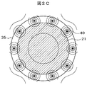
また、試料台18の外周部には誘電体製の絶縁リング35が載置されている。この絶縁リング35には、図2Aに示すように同心円状に添加ガスを供給するためのガス導入用穴40が56個等間隔で配置されており、ガス供給機構36から供給される添加ガスを試料21の外周部に導入できる構造となっている。この装置を用いて、Φ300mmのシリコン基板上に100nm厚かつ50nm幅のラインパターンの酸化膜マスクを形成した試料をエッチングした。なお、ガス導入用穴は、前記試料の最外周から試料直径の1/5以内の位置が望ましい。
A dielectric insulating
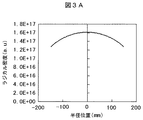
まず、エッチングガスとして、塩素、臭化水素と酸素の混合ガスをガス導入機構19から導入し、ガス導入穴40からは添加ガスは供給せず、プラズマ発生用の高周波電源2からは高周波電圧は印加せず、バイアス用の高周波電源29から高周波電圧を印加してシリコン基板のエッチングを行った。この際の、試料表面近傍の酸素ラジカル濃度分布を図3Aに示す。試料21の中央部で酸素ラジカル濃度が高く、外周部で低くなっていることがわかる。この際の加工後の試料のパターンの寸法の径方向分布を図3Bに示す。パターン寸法は、酸素ラジカル濃度分布と同様に、シリコン基板の中央部で太く、試料の外周部で細くなっていることがわかる。したがって、試料21の外周部で酸素ラジカルの密度が低下していることが原因であることがわかった。
First, as an etching gas, a mixed gas of chlorine, hydrogen bromide and oxygen is introduced from the
そこで、試料外周部の酸素ラジカル密度を増やすべく、ガス導入穴40から酸素ガスを10sccm添加してエッチングした。この際の、試料表面近傍の酸素ラジカル濃度分布を図4Aに示す。酸素ラジカル濃度は全体に増加したが、試料の中央部で酸素ラジカル濃度が高く、外周部で低い状況は変わらない。この際の加工後の試料のパターンの寸法の径方向分布を図4Bに示す。パターン寸法は全体に太くなったが、試料21の中央部が太く、試料の外周部が細い状況は変わっていない。
Therefore, in order to increase the oxygen radical density at the outer periphery of the sample, 10 sccm of oxygen gas was added from the
そこで、さらにプラズマ生成用の高周波電源2から100Wの高周波電力を投入してエッチングを行った。この際の、試料表面近傍の酸素ラジカル濃度分布を図5Aに示す。ウエハ(試料)中央部の酸素ラジカル濃度が減少するとともに外周部の酸素ラジカル濃度が増加して、酸素ラジカル濃度が均一になっていることがわかる。この際の加工後の試料のパターンの寸法の径方向分布を図5Bに示す。試料の外周部のパターンの寸法が増加し、パターン寸法が試料面内でほぼ均一になった。
Therefore, etching was further performed by supplying high-frequency power of 100 W from the high-
つぎに、ガス導入用穴40のピッチの影響について検討した。図2Bおよび図2Cは、ガス導入用穴40の個数がそれぞれ56個の場合および8個の場合のラジカル分布を等高線でそれぞれ表示している。いずれの場合も、穴近傍のラジカル密度が高く離れるにしたがって、低くなっている。図2Bの場合、穴数が多いため、ウエハ面内では同心円状のラジカル分布が実現できている。一方、図2C場合は穴数が少ないため、ウエハ面内でも、ラジカル分布は同心円ではなく、円周方向で濃度の高い部分と低い部分が見られる。この円周方向のラジカル濃度ムラは、穴のピッチaと穴とウエハ(最外周)の間の距離bの比率a/bと非常に密接な相関がある。この関係を調べた結果を図2Dに示す。a/bが小さくなるに従って、ラジカル濃度ムラは低減され、a/bが1以下ではほとんど濃度ムラがなくなっていることがわかる。すなわち、ガス導入用穴40のピッチはウエハと穴の間の距離より短くすることが望ましい。また、穴のピッチを極限まで短くした構造、すなわち、図2Eに示すようにスリット状のガス導入機構にすればさらに均一なガス供給ができると考えられる。 Next, the influence of the pitch of the gas introduction holes 40 was examined. 2B and 2C show the distribution of radicals when the number of gas introduction holes 40 is 56 and 8 respectively, with contour lines. In either case, the radical density in the vicinity of the hole decreases as the distance increases. In the case of FIG. 2B, since the number of holes is large, a concentric radical distribution is realized in the wafer surface. On the other hand, in the case of FIG. 2C, since the number of holes is small, the radical distribution is not concentric even in the wafer surface, and a portion having a high concentration and a portion having a low concentration are seen in the circumferential direction. The uneven radical concentration in the circumferential direction has a very close correlation with the pitch a of the hole and the ratio a / b of the distance b between the hole and the wafer (outermost circumference). The result of examining this relationship is shown in FIG. 2D. It can be seen that as the a / b becomes smaller, the radical concentration unevenness is reduced, and when the a / b is 1 or less, the concentration unevenness is almost eliminated. That is, it is desirable that the pitch of the gas introduction holes 40 be shorter than the distance between the wafer and the holes. Further, it is considered that a more uniform gas can be supplied by using a structure in which the pitch of the holes is shortened to the limit, that is, a slit-like gas introduction mechanism as shown in FIG. 2E.
つぎに、ガス導入穴40の位置の影響について検討した。前述の構成で、ガス導入穴40を誘電体窓26の最外周に設けて、図5Aと同様にウエハ近傍のラジカル濃度分布を調べた結果を図5Cに示す。ラジカル濃度は全体に増加するものの外周部のラジカル濃度が低い状況はそのままである。加工後の試料のパターンの寸法の径方向分布を図5Dに示す。パターン寸法は全体に太くなったが、試料の中央部が太く、試料の外周部が細い状況は変わっていない。すなわち、ガス導入穴40が試料の外周にあっても、試料から離れていると効果が得られないことがわかる。ガス添加の効果の有無を左右しているのが、ガス導入穴40とウエハの間の距離bとガス導入穴40と誘電体窓26の間の距離cである。ウエハ近傍のラジカル濃度分布の均一性とb/(b+c)の関係を図5Eに示す。b/(b+c)が0.5より小さい範囲では、b/(b+c)に比例して、ラジカル濃度分布の均一性もよくなっていることがわかる。すなわち、ガス添加によるラジカル分布均一化の効果をうるには、ガス導入穴40が誘電体窓26よりウエハに近いということが必要条件になることがわかる。
Next, the influence of the position of the
本実施例では、プラズマ発生用の高周波電源2の周波数を40MHzとしたが、4MHz以上の高周波電源であれば、いかなる周波数に設定しても同様の効果が得られる。また、本実施例では、バイアス印加用の高周波電源29の周波数を400kHzとしたが、100kHz以上で、かつ、プラズマ発生用の高周波電源2の周波数より低ければ、いかなる周波数に設定しても同様の効果が得られる。また、本実施例では試料台18の外周部に載置した絶縁リング35の上に、添加ガス用のガス導入穴40を設けたが、試料の外周でかつ、誘電体窓26より試料21に近い位置であれば同様の効果がある。ガス導入穴40のピッチに関しては、ガス導入穴40と試料間の距離よりも、ピッチが短ければ同様の効果が得られる。また、本実施例では、誘導結合プラズマ方式のプラズマエッチング装置を用いたが、無電極放電方式のプラズマエッチング装置であれば、同様の効果が得られる。本実施例では、添加ガスとして酸素を用いたが、エッチングガスや試料構造が異なれば、他の添加ガスでも同様の効果が得られる。
In this embodiment, the frequency of the high-
以上、本実施例によれば、無電極方式のプラズマエッチング装置において、試料外周周辺でラジカルを発生させることによりラジカル密度を均一化し、エッチングの均一性を向上させることのできるプラズマエッチング装置を提供することができる。また、バイアス印加用の高周波電圧とプラズマ発生用の高周波電電圧の両者を試料台に印加するため、構造が単純でありコストの増加を低減できる。 As described above, according to the present embodiment, in an electrodeless plasma etching apparatus, a plasma etching apparatus is provided that can generate radicals around the outer periphery of the sample to make the radical density uniform and improve the etching uniformity. be able to. In addition, since both the high-frequency voltage for bias application and the high-frequency electric voltage for plasma generation are applied to the sample stage, the structure is simple and the increase in cost can be reduced.
本発明の第2の実施例について図6〜図9Bを用いて説明する。なお、実施例1に記載され本実施例に未記載の事項は特段の事情が無い限り本実施例にも適用することができる。図6は、本実施例に係る有磁場マイクロ波プラズマエッチング装置の全体概略構成図である。このプラズマエッチング装置では、エッチングガスは、ガス供給ユニット16から、石英製の誘電体窓26の内部に作られたガス貯め10を経て、誘電体窓26の減圧処理室側に設けられた複数の穴11(シャワープレート構造)から、減圧処理室20の内部に導入される。また、ターボ分子ポンプ22と圧力制御用可変バルブ23によって減圧処理室20の排気速度を調整することによって、処理室内のエッチングガスの圧力を所望のちに設定することができる。また、マグネトロン53で生成されたマイクロ波が導波管54、空洞共振部55、誘電体窓26を経て、減圧処理室内に供給される構造になっており、このマイクロ波が作る横方向の電界と、コイル56の作る縦方向の静磁場の相互作用によって処理室上部にプラズマ生成部17を形成できる構造になっている。
A second embodiment of the present invention will be described with reference to FIGS. Note that the matters described in the first embodiment but not described in the present embodiment can be applied to the present embodiment as long as there is no particular circumstance. FIG. 6 is an overall schematic configuration diagram of a magnetic field microwave plasma etching apparatus according to the present embodiment. In this plasma etching apparatus, an etching gas is supplied from a
このプラズマ生成部17でエッチングガスからイオンとラジカルを生成し、このイオンとラジカルを拡散により輸送し、試料台18に載置された試料21に照射できる構造になっている。また、試料台18にはバイアス印加用の400kHzの高周波電源29が整合器30とローパスフィルタ31を介して取り付けられており、この高周波電源29から高周波電圧を印加することによって、試料21に負電圧を発生させ、減圧処理室20の内部の正イオンを加速して照射することができる。これとは別に、プラズマ発生用の27MHzの高周波電源2が整合器32とハイパスフィルタ33を介して試料台18に接続されており、この高周波電源2から高周波電力を投入することによって試料21の外周部にリング状のプラズマ生成領域1を形成することができる。特に有磁場マイクロ波プラズマエッチング装置のように減圧処理室内に縦方向の静磁場を有する装置では、プラズマ発生用の高周波電源2から供給される電力が試料21の外周部に作る横方向の電界と、コイル56の作る縦方向の静磁場の相互作用によって、試料21の外周部のみに効率的にプラズマを生成することができる。このように周波数の異なる二つの高周波電源2および29を試料台18に取り付けることによって、正イオンを加速するための負電圧とプラズマ発生を独立に制御できる特徴がある。
The
また、試料台18の外周部には誘電体製の絶縁リング35が載置されている。実施例1の図2Aと同様に、この絶縁リング35には、図2Aに示すように同心円状に添加ガスを供給するためのガス導入穴40が配置されており、ガス供給機構36から供給される添加ガスを試料21の外周部に導入できる構造となっている。
A dielectric insulating
この装置を用いて、Φ300mmのシリコンウエハ上に300nm厚のSi3N4膜を堆積させ、その上に200nm厚かつ50nm幅のラインパターンの有機材料のマスクを形成した試料をエッチングした。 Using this apparatus, a Si3N4 film having a thickness of 300 nm was deposited on a Φ300 mm silicon wafer, and a sample having a 200 nm thick and 50 nm wide line pattern organic material mask formed thereon was etched.
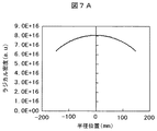
まず、エッチングガスとして、ガス供給機構16からCHF3とArの混合ガスを供給し、ガス導入穴40からは添加ガスは供給せず、プラズマ発生用の高周波電源2からは高周波電力を供給せず、バイアス用の400kHzの高周波電源29からのみ高周波電圧を印加してエッチングを行った。この際の、試料表面近傍のCxFy系ラジカル濃度分布を図7Aに示す。試料21の中央部でラジカル濃度が高く、外周部で低くなっていることがわかるこの際の加工後の試料21のパターンの寸法の径方向分布を図7Bに示す。パターン寸法は、CxFy系ラジカル濃度分布と同様に、試料21の中央部で太く、試料21の外周部で細くなっていることがわかる。すなわち、試料21の外周部でCxFy系のラジカルの密度が低下していることが原因であることがわかった。
First, as an etching gas, a mixed gas of CHF3 and Ar is supplied from the
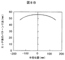
そこで、試料外周部のCxFy系のラジカルの密度を増やすべく、添加ガス導入用のガス導入穴40からCH2F2を10sccm添加してエッチングした。この際の、試料表面近傍のラジカル濃度分布を図8Aに示す。CxFy系ラジカル濃度は全体に増加したが、試料21の中央部でラジカル濃度が高く、外周部で低い状況は変わらない。この際の加工後の試料のパターンの寸法の径方向分布を図8Bに示す。パターン寸法は全体に太くなったが、試料21の中央部が太く、試料21の外周部が細い状況は変わっていない。
Therefore, in order to increase the density of CxFy-based radicals on the outer periphery of the sample, 10 sccm of CH2F2 was added from the
そこで、さらにプラズマ生成用の高周波電源2から50Wの高周波電力を投入してエッチングを行った。試料21の外周部のパターンの寸法が増加し、パターン寸法が試料面内でほぼ均一になった。
Therefore, etching was performed by supplying 50 W of high frequency power from the high
そこで、さらにプラズマ生成用の高周波電源2から100Wの高周波電力を投入してエッチングを行った。この際の、試料表面近傍のCxFy系ラジカル濃度分布を図9Aに示す。ウエハ(試料)中央部のラジカル濃度が減少するとともに外周部のラジカル濃度が増加して、ラジカル濃度が均一になっていることがわかる。この際の加工後の試料のパターンの寸法の径方向分布を図9Bに示す。試料の外周部のパターンの寸法が増加し、パターン寸法が試料面内でほぼ均一になった。
Therefore, etching was further performed by supplying high-frequency power of 100 W from the high-
本実施例では、プラズマ発生用の高周波電源2の周波数を27MHzとしたが、4MHz以上の高周波電源であれば、いかなる周波数に設定しても同様の効果が得られる。また、本実施例では、バイアス印加用の高周波電源29の周波数を400KHzとしたが、100kHz以上で、かつ、プラズマ発生用の高周波電源2の周波数より低ければ、いかなる周波数に設定しても同様の効果が得られる。また、本実施例では試料台18の外周部に載置した絶縁リング35の上に、添加ガス用のガス導入穴40を設けたが、試料の外周でかつ、誘電体窓26より試料21に近い位置であれば同様の効果がある。また、本実施例では、有磁場マイクロ波プラズマ方式のプラズマエッチング装置を用いたが、無電極放電方式のプラズマエッチング装置であれば、同様の効果が得られる。本実施例では、添加ガスとしてCH2F2を用いたが、フロロカーボンガスであれば同様の効果が得られる。また、エッチングガスや試料構造が異なれば、他の添加ガスでも同様の効果が得られる。
In this embodiment, the frequency of the high-
以上、本実施例によれば、無電極方式のプラズマエッチング装置において、試料外周周辺でラジカルを発生させることによりラジカル密度を均一化し、エッチングの均一性を向上させることのできるプラズマエッチング装置を提供することができる。また、バイアス印加用の高周波電圧とプラズマ発生用の高周波電電圧の両者を試料台に印加するため、構造が単純でありコストの増加を低減できる。 As described above, according to the present embodiment, in an electrodeless plasma etching apparatus, a plasma etching apparatus is provided that can generate radicals around the outer periphery of the sample to make the radical density uniform and improve the etching uniformity. be able to. In addition, since both the high-frequency voltage for bias application and the high-frequency electric voltage for plasma generation are applied to the sample stage, the structure is simple and the increase in cost can be reduced.
本発明の第3の実施例について図10〜図13を用いて説明する。なお、実施例1又は2に記載され本実施例に未記載の事項は特段の事情が無い限り本実施例にも適用することができる。図10は、本実施例に係るマイクロ波エッチング装置の全体概略構成図である。このプラズマエッチング装置では、エッチングガスは、ガス供給ユニット16から、石英製の誘電体窓26の内部に作られたガス貯め10を経て、誘電体窓26の減圧処理室側に設けられた複数の穴11(シャワープレート構造)から、減圧処理室20の内部に導入される。また、ターボ分子ポンプ22と圧力制御用可変バルブ23によって減圧処理室20の排気速度を調整することによって、減圧処理室内のエッチングガスの圧力を所望のちに設定することができる。また、マグネトロン53で生成されたマイクロ波が導波管54、空洞共振部55、誘電体窓26を経て、減圧処理室内に供給される構造になっており、投入されたマイクロ波の電力によって誘電体窓26の近傍にプラズマ生成部17を形成できる構造になっている。
A third embodiment of the present invention will be described with reference to FIGS. Note that matters described in the first or second embodiment but not described in the present embodiment can also be applied to the present embodiment unless there are special circumstances. FIG. 10 is an overall schematic configuration diagram of the microwave etching apparatus according to the present embodiment. In this plasma etching apparatus, an etching gas is supplied from a
このプラズマ生成部17でエッチングガスからイオンとラジカルを生成し、このイオンとラジカルを拡散により輸送し、試料台18に載置された試料21に照射できる構造になっている。また、試料台18にはバイアス印加用の400kHzの高周波電源29が整合器30とローパスフィルタ31を介して取り付けられており、この高周波電源29から高周波電圧を印加することによって、試料21に負電圧を発生させ、減圧処理室20の内部の正イオンを加速して照射することができる。
The
また、試料台18の外周部には誘電体製の絶縁リング35が載置されている。実施例1の図と同様に、この絶縁リング35には、図2Aに示すように同心円状に添加ガスを供給するためのガス導入穴40が配置されており、ガス供給機構36から供給される添加ガスを試料21の外周部に導入できる構造となっている。
A dielectric insulating
また、絶縁リング上には、ガス導入穴40の外側には試料台18から絶縁された電極41が搭載されている。この電極41には、プラズマ発生用の27MHzの高周波電源2が整合器32とハイパスフィルタ33を介して試料台18に接続されており、この高周波電源2から高周波電力を投入することによって試料21の外周部にプラズマ生成領域1を形成することができる。このように試料台18および絶縁された電極41にそれぞれ周波数の異なる二つの高周波電源2および29を取り付けることによって、正イオンを加速するための負電圧とプラズマ発生を独立に制御できる特徴がある。
On the insulating ring, an
この装置を用いて、Φ300mmのシリコンウエハ上に300nm厚の有機膜を堆積させ、その上に20nm厚かつ50nm幅のラインパターンのSiO2のマスクを形成した試料をエッチングした。
Using this apparatus, an organic film having a thickness of 300 nm was deposited on a silicon wafer having a diameter of 300 mm, and a sample on which a
まず、エッチングガスとして、O2とArの混合ガスを用い、添加ガスは供給せず、プラズマ発生用の27MHzの高周波電圧は印加せず、バイアス用の400kHzの高周波電圧を印加してエッチングを行った。加工後の試料21の外周部の有機膜の加工形状を図11に示す。有機膜のパターン60が試料21の中心部に向かって倒れていることがわかる。有機膜のパターンは酸素ラジカル密度分布が不均一になると倒れやすいことがわかっている。研究の結果、試料21の中央部に比べ、外周部の酸素ラジカル密度が低くなっており、酸素ラジカル密度分布が不均一になっていることが確認された。
First, a mixed gas of
そこで、試料21の外周部の酸素ラジカルの密度を増やすべく、添加ガス導入用のガス導入穴40から酸素を10sccm添加してエッチングした。加工後の試料21の外周部の有機膜の加工形状を図12に示す。有機膜のパターン60が試料21の中心部に向かって倒れていることがわかる。研究の結果、この方法では、試料21の外周部の酸素ラジカル密度が十分増えないことがわかった。
Therefore, in order to increase the density of oxygen radicals on the outer peripheral portion of the
そこで、さらにプラズマ生成用の高周波電源2から100Wの高周波電力を投入してエッチングを行った。この際の加工後の形状を図13に示す。この場合には試料中心部へ向かう倒れは見られなかった。また、試料の外周部のパターンの寸法が増加し、パターン寸法が試料面内でほぼ均一になった。なお、加工後の断面形状に関し、実施例1におけるシリコン基板のエッチングや実施例2におけるSi3N4膜のエッチングでも同様である。
Therefore, etching was further performed by supplying high-frequency power of 100 W from the high-
本実施例では、プラズマ発生用の高周波電源2の周波数を27MHzとしたが、4MHz以上の高周波電源であれば、いかなる周波数に設定しても同様の効果が得られる。また、本実施例では、バイアス印加用の高周波電源29の周波数を400KHzとしたが、100kHz以上で、かつ、プラズマ発生用の高周波電源2の周波数より低ければ、いかなる周波数に設定しても同様の効果が得られる。また、本実施例では試料台18の外周部に載置した絶縁リング35の上に、添加ガス用のガス導入穴40を設けたが、試料の外周でかつ、誘電体窓26より試料21に近い位置であれば同様の効果がある。また、本実施例では、マイクロ波プラズマ方式のプラズマエッチング装置を用いたが、無電極放電方式のプラズマエッチング装置であれば、同様の効果が得られる。本実施例では、添加ガスとして酸素を用いたが、エッチングガスや試料構造が異なれば、他の添加ガスでも同様の効果が得られる。
In this embodiment, the frequency of the high-
以上、本実施例によれば、無電極方式のプラズマエッチング装置において、試料外周周辺でラジカルを発生させることによりラジカル密度を均一化し、エッチングの均一性を向上させることのできるプラズマエッチング装置を提供することができる。また、試料周辺のプラズマ発生領域形成用電極を試料台と絶縁して設けることにより、正イオンを加速するための負電圧とプラズマ発生を独立に制御することができる。 As described above, according to the present embodiment, in an electrodeless plasma etching apparatus, a plasma etching apparatus is provided that can generate radicals around the outer periphery of the sample to make the radical density uniform and improve the etching uniformity. be able to. In addition, by providing the plasma generating region forming electrode around the sample and being insulated from the sample stage, the negative voltage for accelerating positive ions and the plasma generation can be controlled independently.
なお、本発明は上記した実施例に限定されるものではなく、様々な変形例が含まれる。例えば、上記した実施例は本発明を分かりやすく説明するために詳細に説明したものであり、必ずしも説明した全ての構成を備えるものに限定されるものではない。また、ある実施例の構成の一部を他の実施例の構成に置き換えることも可能であり、また、ある実施例の構成に他の実施例の構成を加えることも可能である。また、各実施例の構成の一部について、他の構成の追加・削除・置換をすることが可能である。 In addition, this invention is not limited to an above-described Example, Various modifications are included. For example, the above-described embodiments have been described in detail for easy understanding of the present invention, and are not necessarily limited to those having all the configurations described. Further, a part of the configuration of a certain embodiment can be replaced with the configuration of another embodiment, and the configuration of another embodiment can be added to the configuration of a certain embodiment. Further, it is possible to add, delete, and replace other configurations for a part of the configuration of each embodiment.
1…プラズマ生成領域、2…高周波電源、10…ガス貯め、11…ガス穴、13…アンテナコイル、15…高周波電源、16…ガス供給機構(ユニット)、17…プラズマ生成部、18…試料台、19…ガス導入機構、20…減圧処理室、21…試料、22…ターボ分子ポンプ、23…圧力制御用可変バルブ、24…圧力計、26…誘電体窓、29…高周波電源、30…整合器、31…ローパスフィルタ、32…整合器、33…ハイパスフィルタ、35…絶縁リング、36…ガス供給機構、40…ガス導入穴、41…電極、53…マグネトロン、54…導波管、55…空洞共振部、56…コイル、60…有機膜のパターン。
DESCRIPTION OF
Claims (10)
前記減圧処理室内に第二のガスを前記誘電体窓よりも前記試料に近い位置から供給する第二のガス導入機構と、前記試料台に第一の高周波電源とは異なる周波数のものであって前記試料の外周周辺にプラズマを発生させるための第二の高周波電力を供給する第二の高周波電源とを備えたことを特徴とするプラズマエッチング装置。 A vacuum processing chamber, a first gas introduction mechanism for supplying a first gas, and the dielectric window in which the plasma is generated in the inside by an electric field supplied from the outside to constitute the vacuum treatment chamber, the A sample stage placed in an upper surface of a sample placed in a decompression chamber and processed by the plasma, and a first high-frequency power for generating a bias voltage for the sample during the process is supplied to the sample stage. In a plasma etching apparatus equipped with a first high frequency power supply
A second second gas introduction mechanism for supplying gas from a position closer to the sample than the dielectric window into the vacuum processing chamber, there is a frequency different from the first high-frequency power to the sample stage plasma etching apparatus characterized by comprising a second and a high frequency power source for supplying a second high-frequency power for generating plasma to the periphery around the sample.
前記第二のガスは、前記試料の最外周から前記試料直径の1/5以内の位置から供給されるものであることを特徴とするプラズマエッチング装置。 The plasma etching apparatus according to claim 1, wherein
The plasma etching apparatus, wherein the second gas is supplied from a position within 1/5 of the sample diameter from the outermost periphery of the sample.
前記第二の高周波電力の周波数が4MHz以上で、かつ、前記第一の高周波電力の周波数が前記第二の高周波電力の周波数より低いことを特徴とするプラズマエッチング装置。 In the plasma etching apparatus according to claim 1 or 2 ,
A plasma etching apparatus, wherein the frequency of the second high frequency power is 4 MHz or more , and the frequency of the first high frequency power is lower than the frequency of the second high frequency power .
前記プラズマを生成するための電界がマイクロ波のものであって、かつ、前記減圧処理室内に磁場を供給するためのソレノイドコイルとを備えたことを特徴とするプラズマエッチング装置。 In the plasma etching apparatus according to any one of claims 1 to 3 ,
Be those electric field for generating the plasma is a microwave, and a plasma etching apparatus is characterized in that a order of Soviet Renoidokoiru to supply a magnetic field to the vacuum processing chamber.
前記試料台の外周部に誘電体製のリングを有しており、このリング上に前記第二のガスの導入穴を有することを特徴とするプラズマエッチング装置。 The plasma etching apparatus according to claim 1, wherein
A plasma etching apparatus comprising a dielectric ring on an outer peripheral portion of the sample stage, and an introduction hole for the second gas on the ring.
前記試料台の外周部に誘電体製のリングを有しており、このリング上に前記第二のガスの導入穴を有することを特徴とするプラズマエッチング装置。 In the plasma etching apparatus according to claim 3,
A plasma etching apparatus comprising a dielectric ring on an outer peripheral portion of the sample stage, and an introduction hole for the second gas on the ring.
前記第二のガスの導入穴は、前記リング内に設けられた円周状のスリットであることを特徴とするプラズマエッチング装置。 The plasma etching apparatus according to claim 5, wherein
The plasma etching apparatus according to claim 1, wherein the second gas introduction hole is a circumferential slit provided in the ring.
前記第二のガスの導入穴は、ピッチaで前記リングに沿い、かつ前記試料の最外周からの距離がbとなるように配置され、a/bが1以下であることを特徴とするプラズマエッチング装置。 The plasma etching apparatus according to claim 5, wherein
The second gas introduction hole is disposed along the ring at a pitch a so that the distance from the outermost periphery of the sample is b, and a / b is 1 or less. Etching equipment.
前記第二のガスの導入穴は、前記試料の最外周からの距離がb、前記誘電体窓からの距離がcとなるように配置され、b/(b+c)が0.5以下であることを特徴とするプラズマエッチング装置。 The plasma etching apparatus according to claim 5, wherein
The second gas introduction hole is arranged such that the distance from the outermost periphery of the sample is b and the distance from the dielectric window is c, and b / (b + c) is 0.5 or less. A plasma etching apparatus.
前記第二のガスは、酸素ガスもしくはフロロカーボンガスであることを特徴とするプラズマエッチング装置。 The plasma etching apparatus according to claim 1, wherein
The plasma etching apparatus, wherein the second gas is oxygen gas or fluorocarbon gas.
Priority Applications (4)
| Application Number | Priority Date | Filing Date | Title |
|---|---|---|---|
| JP2011221688A JP5819154B2 (en) | 2011-10-06 | 2011-10-06 | Plasma etching equipment |
| US13/592,129 US20130087285A1 (en) | 2011-10-06 | 2012-08-22 | Plasma etching apparatus |
| US15/370,486 US9960014B2 (en) | 2011-10-06 | 2016-12-06 | Plasma etching method |
| US15/951,814 US10418224B2 (en) | 2011-10-06 | 2018-04-12 | Plasma etching method |
Applications Claiming Priority (1)
| Application Number | Priority Date | Filing Date | Title |
|---|---|---|---|
| JP2011221688A JP5819154B2 (en) | 2011-10-06 | 2011-10-06 | Plasma etching equipment |
Publications (3)
| Publication Number | Publication Date |
|---|---|
| JP2013084653A JP2013084653A (en) | 2013-05-09 |
| JP2013084653A5 JP2013084653A5 (en) | 2014-11-20 |
| JP5819154B2 true JP5819154B2 (en) | 2015-11-18 |
Family
ID=48041303
Family Applications (1)
| Application Number | Title | Priority Date | Filing Date |
|---|---|---|---|
| JP2011221688A Active JP5819154B2 (en) | 2011-10-06 | 2011-10-06 | Plasma etching equipment |
Country Status (2)
| Country | Link |
|---|---|
| US (3) | US20130087285A1 (en) |
| JP (1) | JP5819154B2 (en) |
Families Citing this family (8)
| Publication number | Priority date | Publication date | Assignee | Title |
|---|---|---|---|---|
| JP5819154B2 (en) * | 2011-10-06 | 2015-11-18 | 株式会社日立ハイテクノロジーズ | Plasma etching equipment |
| KR101452828B1 (en) * | 2012-08-28 | 2014-10-23 | 주식회사 유진테크 | Apparatus for processing substrate |
| JP6539113B2 (en) | 2015-05-28 | 2019-07-03 | 株式会社日立ハイテクノロジーズ | Plasma processing apparatus and plasma processing method |
| JP6595335B2 (en) * | 2015-12-28 | 2019-10-23 | 株式会社日立ハイテクノロジーズ | Plasma processing equipment |
| AU2021349358A1 (en) | 2020-09-24 | 2023-02-09 | 6K Inc. | Systems, devices, and methods for starting plasma |
| KR20230095080A (en) | 2020-10-30 | 2023-06-28 | 6케이 인크. | Systems and methods for synthesizing spheroidized metal powders |
| JP2022107873A (en) * | 2021-01-12 | 2022-07-25 | 東京エレクトロン株式会社 | Substrate processing device and cleaning method |
| US20230411123A1 (en) * | 2022-06-09 | 2023-12-21 | 6K Inc. | Plasma apparatus and methods for processing feed material utilizing an upstream swirl module and composite gas flows |
Family Cites Families (25)
| Publication number | Priority date | Publication date | Assignee | Title |
|---|---|---|---|---|
| JP2894658B2 (en) * | 1992-01-17 | 1999-05-24 | 株式会社東芝 | Dry etching method and apparatus |
| JP2870719B2 (en) * | 1993-01-29 | 1999-03-17 | 東京エレクトロン株式会社 | Processing equipment |
| US5498313A (en) * | 1993-08-20 | 1996-03-12 | International Business Machines Corp. | Symmetrical etching ring with gas control |
| US5744049A (en) * | 1994-07-18 | 1998-04-28 | Applied Materials, Inc. | Plasma reactor with enhanced plasma uniformity by gas addition, and method of using same |
| JPH09115880A (en) * | 1995-10-16 | 1997-05-02 | Hitachi Ltd | Dry etching apparatus |
| JPH1064881A (en) * | 1996-08-20 | 1998-03-06 | Hitachi Ltd | Plasma etching device, and plasma etching method |
| US6042687A (en) * | 1997-06-30 | 2000-03-28 | Lam Research Corporation | Method and apparatus for improving etch and deposition uniformity in plasma semiconductor processing |
| US6263829B1 (en) * | 1999-01-22 | 2001-07-24 | Applied Materials, Inc. | Process chamber having improved gas distributor and method of manufacture |
| JP2001185542A (en) * | 1999-12-27 | 2001-07-06 | Hitachi Ltd | Plasma processor and plasma processing method using the same |
| KR100406173B1 (en) * | 2000-06-13 | 2003-11-19 | 주식회사 하이닉스반도체 | Heater Block Having Catalyst Injection means |
| JP4717295B2 (en) * | 2000-10-04 | 2011-07-06 | 株式会社半導体エネルギー研究所 | Dry etching apparatus and etching method |
| US6676760B2 (en) * | 2001-08-16 | 2004-01-13 | Appiled Materials, Inc. | Process chamber having multiple gas distributors and method |
| US20040025791A1 (en) * | 2002-08-09 | 2004-02-12 | Applied Materials, Inc. | Etch chamber with dual frequency biasing sources and a single frequency plasma generating source |
| US6942816B2 (en) | 2003-02-12 | 2005-09-13 | Lam Research Corporation | Methods of reducing photoresist distortion while etching in a plasma processing system |
| CN100463112C (en) * | 2003-05-30 | 2009-02-18 | 周星工程股份有限公司 | Apparatus for semiconductor device |
| JP4566789B2 (en) * | 2005-03-07 | 2010-10-20 | 株式会社日立ハイテクノロジーズ | Plasma processing method and plasma processing apparatus |
| JP4590363B2 (en) * | 2005-03-16 | 2010-12-01 | 日本碍子株式会社 | Gas supply member and processing apparatus using the same |
| US8097120B2 (en) * | 2006-02-21 | 2012-01-17 | Lam Research Corporation | Process tuning gas injection from the substrate edge |
| US20070245958A1 (en) * | 2006-04-24 | 2007-10-25 | Applied Materials, Inc. | Dual plasma source process using a variable frequency capacitively coupled source for controlling ion radial distribution |
| US20080073032A1 (en) * | 2006-08-10 | 2008-03-27 | Akira Koshiishi | Stage for plasma processing apparatus, and plasma processing apparatus |
| JP5074741B2 (en) * | 2006-11-10 | 2012-11-14 | 株式会社日立ハイテクノロジーズ | Vacuum processing equipment |
| JP2010016124A (en) * | 2008-07-02 | 2010-01-21 | Hitachi High-Technologies Corp | Plasma treatment device, and plasma treatment method |
| TWI539517B (en) * | 2010-02-12 | 2016-06-21 | 應用材料股份有限公司 | Kit for use in processing chamber and processing chamber using kit for gas flow improvements |
| JP5819154B2 (en) * | 2011-10-06 | 2015-11-18 | 株式会社日立ハイテクノロジーズ | Plasma etching equipment |
| JP6120527B2 (en) * | 2012-11-05 | 2017-04-26 | 東京エレクトロン株式会社 | Plasma processing method |
-
2011
- 2011-10-06 JP JP2011221688A patent/JP5819154B2/en active Active
-
2012
- 2012-08-22 US US13/592,129 patent/US20130087285A1/en not_active Abandoned
-
2016
- 2016-12-06 US US15/370,486 patent/US9960014B2/en active Active
-
2018
- 2018-04-12 US US15/951,814 patent/US10418224B2/en active Active
Also Published As
| Publication number | Publication date |
|---|---|
| US9960014B2 (en) | 2018-05-01 |
| US20130087285A1 (en) | 2013-04-11 |
| JP2013084653A (en) | 2013-05-09 |
| US20180233329A1 (en) | 2018-08-16 |
| US20170084430A1 (en) | 2017-03-23 |
| US10418224B2 (en) | 2019-09-17 |
Similar Documents
| Publication | Publication Date | Title |
|---|---|---|
| JP5819154B2 (en) | Plasma etching equipment | |
| JP5264231B2 (en) | Plasma processing equipment | |
| US8222157B2 (en) | Hybrid RF capacitively and inductively coupled plasma source using multifrequency RF powers and methods of use thereof | |
| JP5931063B2 (en) | Plasma processing apparatus and plasma processing method | |
| JP5514310B2 (en) | Plasma processing method | |
| KR102390726B1 (en) | Method for etching organic film | |
| JP2006203210A (en) | Semiconductor plasma processing device and method | |
| JP2013254723A (en) | Plasma processing apparatus | |
| TWI594322B (en) | Plasma processing method and plasma processing apparatus | |
| JP2009123929A (en) | Plasma treatment apparatus | |
| JP4935149B2 (en) | Electrode plate for plasma processing and plasma processing apparatus | |
| KR102418243B1 (en) | Plasma processing apparatus and plasma processing method | |
| JP2012049376A (en) | Plasma processing apparatus and plasma processing method | |
| JP4336680B2 (en) | Reactive ion etching system | |
| JP6763750B2 (en) | How to process the object to be processed | |
| JP2000031121A (en) | Plasma discharger and plasma treating device | |
| JP6317921B2 (en) | Plasma processing equipment | |
| JP3940467B2 (en) | Reactive ion etching apparatus and method | |
| JP6595335B2 (en) | Plasma processing equipment | |
| US20220262601A1 (en) | Etching method and plasma processing apparatus | |
| KR102118405B1 (en) | Plasma processing apparatus and plasma processing method | |
| JP2023541910A (en) | Non-uniformity control of plasma discharge using magnetic field | |
| JP2016134460A (en) | Plasma processing device and plasma processing method | |
| JP2015198083A (en) | Plasma processing apparatus and plasma processing method | |
| JP2016213404A (en) | Plasma etching method |
Legal Events
| Date | Code | Title | Description |
|---|---|---|---|
| A521 | Written amendment |
Free format text: JAPANESE INTERMEDIATE CODE: A523 Effective date: 20141002 |
|
| A621 | Written request for application examination |
Free format text: JAPANESE INTERMEDIATE CODE: A621 Effective date: 20141002 |
|
| A977 | Report on retrieval |
Free format text: JAPANESE INTERMEDIATE CODE: A971007 Effective date: 20150602 |
|
| A131 | Notification of reasons for refusal |
Free format text: JAPANESE INTERMEDIATE CODE: A131 Effective date: 20150609 |
|
| A521 | Written amendment |
Free format text: JAPANESE INTERMEDIATE CODE: A523 Effective date: 20150803 |
|
| TRDD | Decision of grant or rejection written | ||
| A01 | Written decision to grant a patent or to grant a registration (utility model) |
Free format text: JAPANESE INTERMEDIATE CODE: A01 Effective date: 20150901 |
|
| A61 | First payment of annual fees (during grant procedure) |
Free format text: JAPANESE INTERMEDIATE CODE: A61 Effective date: 20150930 |
|
| R150 | Certificate of patent or registration of utility model |
Ref document number: 5819154 Country of ref document: JP Free format text: JAPANESE INTERMEDIATE CODE: R150 |
|
| S531 | Written request for registration of change of domicile |
Free format text: JAPANESE INTERMEDIATE CODE: R313531 |
|
| S533 | Written request for registration of change of name |
Free format text: JAPANESE INTERMEDIATE CODE: R313533 |
|
| R350 | Written notification of registration of transfer |
Free format text: JAPANESE INTERMEDIATE CODE: R350 |