JP5817552B2 - Electronic equipment - Google Patents
Electronic equipment Download PDFInfo
- Publication number
- JP5817552B2 JP5817552B2 JP2012011308A JP2012011308A JP5817552B2 JP 5817552 B2 JP5817552 B2 JP 5817552B2 JP 2012011308 A JP2012011308 A JP 2012011308A JP 2012011308 A JP2012011308 A JP 2012011308A JP 5817552 B2 JP5817552 B2 JP 5817552B2
- Authority
- JP
- Japan
- Prior art keywords
- cooling
- electronic
- electronic component
- air
- cooling plate
- Prior art date
- Legal status (The legal status is an assumption and is not a legal conclusion. Google has not performed a legal analysis and makes no representation as to the accuracy of the status listed.)
- Active
Links
- 238000001816 cooling Methods 0.000 claims description 184
- 239000000758 substrate Substances 0.000 claims description 62
- XLYOFNOQVPJJNP-UHFFFAOYSA-N water Substances O XLYOFNOQVPJJNP-UHFFFAOYSA-N 0.000 claims description 35
- 239000000498 cooling water Substances 0.000 claims description 27
- 239000003990 capacitor Substances 0.000 claims description 21
- 230000005669 field effect Effects 0.000 claims description 16
- 238000010438 heat treatment Methods 0.000 claims description 4
- 238000012545 processing Methods 0.000 claims description 3
- 238000007789 sealing Methods 0.000 claims description 2
- 230000003321 amplification Effects 0.000 description 23
- 238000003199 nucleic acid amplification method Methods 0.000 description 23
- 238000012546 transfer Methods 0.000 description 18
- 239000000463 material Substances 0.000 description 8
- 238000005192 partition Methods 0.000 description 5
- 229910052782 aluminium Inorganic materials 0.000 description 3
- XAGFODPZIPBFFR-UHFFFAOYSA-N aluminium Chemical compound [Al] XAGFODPZIPBFFR-UHFFFAOYSA-N 0.000 description 3
- 230000005540 biological transmission Effects 0.000 description 3
- 239000000470 constituent Substances 0.000 description 3
- 238000010586 diagram Methods 0.000 description 3
- 230000000694 effects Effects 0.000 description 3
- 229910052751 metal Inorganic materials 0.000 description 3
- 239000002184 metal Substances 0.000 description 3
- 239000012466 permeate Substances 0.000 description 3
- 239000011347 resin Substances 0.000 description 3
- 229920005989 resin Polymers 0.000 description 3
- 206010037660 Pyrexia Diseases 0.000 description 2
- 230000007423 decrease Effects 0.000 description 2
- 230000007613 environmental effect Effects 0.000 description 2
- 238000009413 insulation Methods 0.000 description 2
- 238000000034 method Methods 0.000 description 2
- 238000012986 modification Methods 0.000 description 2
- 230000004048 modification Effects 0.000 description 2
- 229910000679 solder Inorganic materials 0.000 description 2
- 239000004593 Epoxy Substances 0.000 description 1
- 238000007664 blowing Methods 0.000 description 1
- 230000015556 catabolic process Effects 0.000 description 1
- 238000007599 discharging Methods 0.000 description 1
- 230000005670 electromagnetic radiation Effects 0.000 description 1
- 239000011521 glass Substances 0.000 description 1
- 239000004519 grease Substances 0.000 description 1
- 238000012423 maintenance Methods 0.000 description 1
- 238000007747 plating Methods 0.000 description 1
- 229920001721 polyimide Polymers 0.000 description 1
- 230000005855 radiation Effects 0.000 description 1
- 238000004904 shortening Methods 0.000 description 1
Images


Landscapes
- Cooling Or The Like Of Electrical Apparatus (AREA)
Description
本発明は、電子装置に関し、例えば電力増幅装置のように、電子基板を冷却する冷却板を有する電子装置に関する。 The present invention relates to an electronic device, and more particularly to an electronic device having a cooling plate for cooling an electronic substrate, such as a power amplification device.
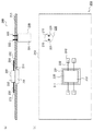
電子装置の一例として、一般的な電力増幅装置2000を説明する。図11は、一般的な電力増幅装置の構成を示す断面図である。
A general
図11に示されるように、一般的な電力増幅装置2000は、冷却板2100と、電子基板2200と、シールド蓋2300とを備えている。
As shown in FIG. 11, a general
電子基板2200は、基材2210上に、電解コンデンサ2220や電界効果トランジスタ(Field effect transistor:FET)2230を有している。
The
電界効果トランジスタ2230は、熱および電磁波を発生し、これらを周囲に輻射する。一般的な電力増幅装置2000では、水冷流路2110を有する冷却板2100が設けられている。そして、この水冷流路2110内に冷却水を流すことにより、電子基板2100を冷却している。また、電界効果トランジスタ2230の伝熱板2231を冷却板2100に直接的に接触させて、電界効果トランジスタ2230を冷却している。
The
また、一般的な電力増幅装置2000では、シールド蓋2300が設けられている。このシールド蓋2300と冷却板2100との間で電子基板2200を密閉することにより、熱や電磁波の輻射を抑止している。また、複数の電界効果トランジスタ2230が基材2210上に実装される場合には、電界効果トランジスタ2230間に仕切り板(不図示)を設けることにより、複数の電界効果トランジスタ2230の間の電磁波の干渉を抑止している。
In general power amplifying
なお、関連技術として、例えば、シールド蓋(ケース21)と冷却板1の間で密閉された電子基板(部品取付板10)を、冷却板1内の冷却流路(給水パイプ4、排水パイプ5)に冷却水を流すことによって、冷却する技術が特許文献1に開示されている。 As a related technique, for example, an electronic substrate (component mounting plate 10) sealed between a shield lid (case 21) and the cooling plate 1 is used as a cooling channel (water supply pipe 4, drain pipe 5) in the cooling plate 1. Patent Document 1 discloses a technique of cooling by flowing cooling water through
しかしながら、一般的な電力増幅装置2000では、シールド蓋2300を設けたことによって、電界効果トランジスタ2230が発する高温の熱がシールド蓋2300と冷却板2100の間で充満してしまう。このため、冷却板2100の水冷流路2120内に冷却水を流したとしても、電子基板2200が電力増幅装置2000外の温度や冷却板2100の温度よりも高くなってしまうことがあった。この結果、電解コンデンサ2220のように熱に弱い電子部品は、高温の環境下に晒されてしまい、破損したり、寿命が短くなったりする問題があった。この場合、電解コンデンサ2220の交換頻度が高くなってしまう問題も生じる。
However, in general power amplifying
また、近年、電力増幅装置2000に対しては、高出力が仕様として要求される傾向にある。また、これに伴って、電解コンデンサ2220も高耐圧、高容量が仕様として要求される傾向にある。このため、電解コンデンサ2220の容量や高さも大きくなり、電子基板2200の基材2210とシールド蓋2300の天面との間の距離を大きくする必要が生じ、電力増幅装置2000の大きさも大きくなってしまう問題があった。
In recent years, the power amplifying
本発明は、このような事情に鑑みてなされたものであり、本発明の目的は、例えば電力増幅装置など、密閉された装置内で使用される電子部品として、例えば電解コンデンサのように熱に弱い電子部品が高温下に晒されてしまい、破損が生じたり、寿命が短くなったりすることと、例えば電力増幅装置の出力などの仕様の要求により電子部品が大きくなり装置全体が大きくなってしまうという課題を解決する電子装置を提供することにある。 The present invention has been made in view of such circumstances, and an object of the present invention is to provide heat, such as an electrolytic capacitor, as an electronic component used in a sealed device such as a power amplifier. Weak electronic components are exposed to high temperatures, resulting in damage or shortening of the life, and due to requirements of specifications such as the output of the power amplification device, the electronic components become larger and the entire device becomes larger An object of the present invention is to provide an electronic device that solves the problem.
本発明の電子装置は、第1の電子部品が実装された電子基板と、熱伝導性を有し、前記電子基板の熱を冷却するように前記電子基板の背面側に設けられた冷却板と、前記冷却板との間で、前記電子基板を密閉して収容するシールド蓋と、前記電子基板の面に沿って前記冷却板内に貫通して形成され、外部の空気を通す空冷流路とを備え、前記第1の電子部品は、前記空冷流路内に配置されている。 An electronic device according to the present invention includes an electronic substrate on which a first electronic component is mounted, a cooling plate having thermal conductivity and provided on the back side of the electronic substrate so as to cool the heat of the electronic substrate. A shield lid for sealingly housing the electronic substrate between the cooling plate, an air cooling passage formed through the cooling plate along the surface of the electronic substrate, and allowing external air to pass through. The first electronic component is disposed in the air cooling channel.
本発明にかかる電子装置によれば、密閉された装置内に配置された電子部品の温度環境が高温にならないように維持して装置全体の品質を高くできるとともに、電子部品の大きさが装置全体の大きさに与える影響を低減できる。 According to the electronic device according to the present invention, the quality of the entire device can be improved by maintaining the temperature environment of the electronic component disposed in the sealed device so as not to become high temperature, and the size of the electronic component can be increased. The influence on the size of can be reduced.
<第1の実施の形態>
本発明の第1の実施の形態における電力増幅装置1000の構成について、図に基づいて説明する。
<First Embodiment>
A configuration of the power amplifying
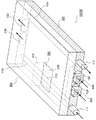
図1は、本発明の第1の実施の形態における電力増幅装置1000の構成を透過して示す透過斜視図である。図2は、電力増幅装置1000の構成を透過して示す透過平面図である。図3は、図2のA−A切断線における断面を示す断面図である。図4は、電子基板200の構成を示す図である。図4(a)は電子基板200の断面図である。図4(b)は電子基板200の平面図である。図5は、冷却板100の構成を示す平面図である。図6は、シールド蓋300の構成を内側から示す平面図である。
FIG. 1 is a transparent perspective view showing the configuration of the power amplifying
図1〜図2に示されるように、電力増幅装置1000は、冷却板100と、電子基板200と、シールド蓋300とを含んで構成されている。
As shown in FIGS. 1 to 2, the power amplifying
以下に、電子基板200、シールド蓋300および冷却板100の各構成について、図に基づいて、順次説明する。
Below, each structure of the electronic board |
まず、電子基板200の構成について説明する。図4(a)および図4(b)に示されるように、電子基板200は、基材210と、第1の電子部品220と、第2の電子部品230とを含んで構成されている。図1〜図3に示されるように、電子基板200は、冷却板100上に取り付けられる。なお、電子基板200は、通常、冷却板100上に複数取り付けられるが、ここでは説明の便宜上、1つの電子基板200が冷却板100上に設けられている例を示す。
First, the configuration of the
基材210は、例えば、板状に形成されたプリント配線基板である。基材210の材料には、ガラスエポキシ板材やポリイミドフィルムなどが用いられる。また、図4(a)および図4(b)に示されるように、基材210には、開口部211が形成されている。この開口部211の大きさは、第2の電子部品230の大きさに対応している。そして、第2の電子部品220が開口部211内に収容される。
The
第1の電子部品220は、例えば電解コンデンサなど、温度制約のある電子部品である。すなわち、第1の電子部品220は、高温下で使用すると、寿命が短縮したり破損したりするおそれがある電子部品である。
The first
図4(a)および図4(b)に示されるように、第1の電子部品220は、回路部221と端子222とを有する。回路部221は、電子回路(不図示)を樹脂などにより被覆して構成されている。第1の電子部品220が例えば電解コンデンサの場合には、回路部221内部には電極板や誘電体などが収容される。端子222は、回路部221内の電子回路に電気的に接続されている。端子222は、基材210上に設けられた電極部213に半田(不図示)などにより接続される。
As shown in FIGS. 4A and 4B, the first
第2の電子部品230は、例えば電界効果トランジスタである。この電界効果トランジスタは、電磁波を周囲に輻射するとともに、RF信号を増幅する際に自ら大量の熱を発生し、この熱を周囲に輻射する。なお、第1の電子部品230は、発熱素子であればよく、電界効果トランジスタの他に、例えば中央演算処理装置(Central Processing Unit:CPU)や、集積回路(Multi-chip Module:MCM)等であってもよい。
The second
図4(a)および図4(b)に示されるように、第2の電子部品230は、伝熱部231と回路部232と端子233を有している。伝熱部231は、金属などの伝熱部材により形成されている。伝熱部231は、図3に示されるように、冷却板100に設けられた受熱部130にグリース等により貼り付けられる。これにより、伝熱部231と受熱部130とが接触し、熱的に接続する。そして、第2の電子部品230の熱が、伝熱部231および受熱部130を介して、冷却板100へ伝達される。回路部232は、電子回路(不図示)を樹脂などにより被覆して構成されている。端子233は、回路部232内の電子回路(不図示)に電気的に接続されている。端子233は、図4(a)および図4(b)に示されるように、基材210上に設けられた電極部212に半田(不図示)などにより接続される。
As shown in FIG. 4A and FIG. 4B, the second
以上、電子基板200の構成について説明した。
The configuration of the
次に、シールド蓋300の構成について、図に基づいて説明する。
Next, the configuration of the
図6に示されるように、シールド蓋300は、天板310と、側板320と、仕切板330とを含んで構成される。側板320は、天板310の外周に沿って設けられている。シールド蓋300には、例えばアルミニウムなどの金属板や、樹脂成形部材にアルミニウムなどの金属メッキを施した部材などを用いることができる。
As shown in FIG. 6, the
図1〜図3に示されるように、シールド蓋300は、冷却板100との間で、電子基板200を密閉する。すなわち、電子基板200は、シールド蓋300と冷却板100との間で構成される密閉空間内に収容される。これにより、電界効果トランジスタ等の第2の電子部品220や電子基板200から放射される電磁波が、電力増幅装置1000の外部に放出されることを抑止できる。
As shown in FIGS. 1 to 3, the
仕切板330は、天板310および側板320に連結されている。例えば電界効果トランジスタのように電磁波を輻射するような電子部品を複数個設ける場合などに、当該電子部品間に仕切板330を設ける。これにより、電子部品間での電磁波の干渉を抑止することができる。
The
以上、シールド蓋300の構成について説明した。
The configuration of the
次に、冷却板100の構成について、図に基づいて説明する。
Next, the structure of the
図1、図2、図3および図5に示されるように、冷却板100は、矩形の平板状に形成されている。また、冷却板100は、例えばアルミニウムなどの熱伝導性を有する部材により構成されている。冷却板100は、図2に示されるように、電子基板200の背面側に設けられており、電子基板200の熱を冷却する。すなわち、電子基板200は、冷却板100の表面側に取り付けられる。
As shown in FIGS. 1, 2, 3, and 5, the
図5に示されるように、冷却板100は、水冷流路110と、空冷流路120と、受熱部130とを含んで構成される。
As shown in FIG. 5, the
水冷流路110は、図5に示されるように、冷却板100内に設けられている。図5では、水冷流路110は、空冷流路120の両側に、英字の「U」の字状に、形成されている。なお、図1および図5に示されるように、水冷流路110の一部は、空冷流路120と干渉しないように、冷却板100から露出されている。水冷流路110は1本に繋がっており、その両端には給水管111および排水管112が設けられている。
As shown in FIG. 5, the
給水管111は、水冷流路110内に冷却水を供給するための入口である。排水管112は、冷却流露110内を循環した後の冷却水を排出するための出口である。
The
図1、図2、図3および図5に示されるように、空冷流路120は、電子基板200の面に沿って冷却板100内に貫通して形成されている。空冷流路120は、外部の空気を通すことができる。また、開口部121は、空冷流路120の途中であって、電子基板100上の第1の電子部品220が配置される位置に対応する領域に、形成されている。そして、図2および図3に示されるように、第1の電子部品220が、開口部121を介して、空冷流路120内に配置される。空冷流路120内は外部の空気によって冷却される。このため、空冷流路120内に配置される第1の電子部品220は、常に外部の空気により冷却された環境下に配置される。これにより、密閉された電力増幅装置1000内に配置された電子基板200上の第1の電子部品220の温度環境が高温にならないように維持することができる。この結果、当該電子部品の寿命が短くなったり、破損したりすることを抑制できる。
As shown in FIG. 1, FIG. 2, FIG. 3, and FIG. 5, the
また、第1の電子部品220が空冷流路120内に配置されることにより、電子基板200の表面(図3の上側の面)上に他の電子部品を実装する領域を確保できる。また、第1の電子部品220が電子基板200の表面側から無くなったことにより、この領域に対応するシールド蓋300の高さ(具体的には、図3にて冷却板100の表面からシールド蓋300の上面までの距離D)を小さくすることができ、電力増幅装置1000の大きさを小さくすることができる。このことは、特に、第1の電子部品220が、電子基板200の表面上に実装された他の電子部品と比較して、最も高い電子部品であった場合に、有効である。すなわち、例えば、第1の電子部品220が電解コンデンサのように背の高い部品であった場合に、当該第1の電子部品220が電子基板200の表面上から無くなることにより、第1の電子部品220の高さに影響を受けることなく、シールド蓋300の高さDを当該シールド蓋300全体に亘って小さくすることができる。この結果、電力増幅装置1000の大きさを全体的に小さくすることができる。
In addition, by arranging the first
図3および図5に示されるように、受熱部130は、冷却板100の表面側に凹形状に設けられている。受熱部130には、第2の電子部品230の伝熱部231が収容される。したがって、受熱部130の大きさや深さは、第2の電子部品230の伝熱部231の大きさや高さに対応している。また、第2の電子部品230の伝熱部231は、受熱部130に収容されたときに、当該受熱部130に接触する。そして、第2の電子部品230の発熱が、伝熱部231および受熱部130を介して、冷却板100へ伝達する。これより、第2の電子部品230の熱が、冷却板110内で放熱される。
As shown in FIGS. 3 and 5, the
また、図2、図3および図5に示されるように、受熱部130は、水冷流路110が設けられた位置に対応して、形成されている。受熱部130は、水冷流路110に対向するように設けられている。すなわち、受熱部130は、水冷流路110に近接して設けられている。前述の通り、水冷流路120には、冷却水が供給される。したがって、第2の電子部品230の熱は、伝熱部231および受熱部130を介して冷却板110へ伝達した後、さらに水冷流路110内を流れる冷却水に伝達される。これにより、第2の電子部品230の熱が放熱される。
In addition, as shown in FIGS. 2, 3, and 5, the
以上、冷却板100の構成について説明した。
The configuration of the
次に、本発明の第1の実施の形態における電力増幅装置1000の動作について、図に基づいて説明する。電力増幅装置1000は、次に説明する通り、冷却装置3000に接続して使用される。
Next, the operation of the
図7は、電力増幅装置1000と冷却装置3000との関係を示す図である。図7に示されるように、電力増幅装置1000と冷却装置3000は、2本の接続管4100、4200により接続されている。
FIG. 7 is a diagram illustrating a relationship between the
ここでは、まず、冷却装置3000の構成を説明し、次に電力増幅装置1000と冷却装置3000の接続関係を説明し、その後に電力増幅装置1000の動作を説明する。
Here, first, the configuration of the
まず、冷却装置3000の構成について図に基づいて説明する。
First, the configuration of the
図7に示されるように、冷却装置3000は、冷却管3100と、ファン部3200と、筐体3300を含んで構成されている。
As shown in FIG. 7, the
冷却管3100は、図7に示されるように、外部の空気に晒されるように露出されて、筐体3300に取り付けられている。冷却管3100は、筐体3300の端部間(図7の紙面にて左右端部)を交互に行き来するように、形成されている。
As shown in FIG. 7, the
冷却管3100の両端部には、給水管3101および排水管3102が取り付けられている。
A
ファン部3200は、冷却管3100に対向するように、筐体3300に取り付けられている。ファン部3200は、冷却管3100に直接、風を当てる。このように、ファン部3200は、冷却管3100に対して送風することにより、冷却管3100内を流れる冷却水を冷却する。
The
以上、冷却装置3000の構成について説明した。
The configuration of the
次に、電力増幅装置1000と冷却装置3000の接続関係について説明する。
Next, the connection relationship between the
図7に示されるように、給水管3101と、電力増幅装置1000の排水管112とが、接続管4200により接続されている。また、排出管3102と、電力増幅装置1000の給水管111とが、接続管4100により接続されている。
As shown in FIG. 7, the
電力増幅装置1000の排水管112から排出される冷却水は、図7の矢印aで示すように、給水管3101から冷却装置3000内に流入する。このとき、電力増幅装置1000の排水管112から排出される冷却水は、電子基板200の熱を吸熱している。冷却装置3000内に流入した冷却水は、冷却管3100内を流れる。このとき、冷却管3100は外気に晒されているので、冷却管3100内を流れる冷却水は外気によって冷却される。冷却管3100内で冷却された冷却水は、排水管3102から排出される。冷却装置3000の排水管3102から排出された冷却水は、図7の矢印bで示すように、給水管111から電力増幅装置1000内に流入する。このように、冷却水が、電力増幅装置1000と冷却装置3000の間を循環する。このとき、冷却水は、電力増幅装置1000内で電子基板200等の熱を吸熱し、冷却装置3000内でファン部3200により冷却される。
The cooling water discharged from the
以上、電力増幅装置1000と冷却装置3000の接続関係について説明した。
The connection relationship between the
次に、電力増幅装置1000の動作について、図に基づいて説明する。
Next, the operation of the
電力増幅装置1000と冷却装置3000の電源が入ると、冷却水が電力増幅装置1000と冷却装置3000の間で循環し始めるとともに、ファン部3200が作動する。
When the power of the
図3に示されるように、電力増幅装置1000内では、第2の電子部品230の伝熱部231と、冷却板100の受熱部130が、互いに接触しており、熱的に接続している。したがって、第2の電子部品230の発熱が、伝熱部231および受熱部130を介して、冷却板100へ伝達する。これより、第2の電子部品230の発熱が、冷却板100内で放熱される。
As shown in FIG. 3, in the
また、図3に示されるように、水冷流路110は、受熱部130の近傍に配置されている。この水冷流路110内には、冷却装置3000により冷却された冷却水が流れている。このため、第2の電子部品230の発熱は、伝熱部231および受熱部130を介して冷却板100へ伝達した後、さらに水冷流路110内を流れる冷却水に伝達される。これにより、第2の電子部品230の熱が放熱される。
In addition, as shown in FIG. 3, the
さらに、図3に示されるように、第1の電子部品220が、開口部121を介して、空冷流路120内に配置される。この空冷流路120は、冷却板100を貫通して形成されているので、外部の空気を通す。このため、空冷流路120は、外部の空気によって冷却されている。したがって、第1の電子部品220は、外部の空気により冷却された空冷流路120内に配置される。
Further, as shown in FIG. 3, the first
第2の電子部品230の熱を吸熱した冷却水は、冷却板100内の水冷流路110内を流れた後、図7に示されるように、接続管4200を介して冷却装置3000内に流入する。
The cooling water that has absorbed the heat of the second
そして、冷却装置3000内では、電力増幅装置1000から流入した冷却水が、冷却管3100を通った後、接続管4100を介して電力増幅装置1000に流入する。このとき、冷却管3100内を流れる冷却水は、ファン部3200による送風によって、冷却される。
In the
以上、電力増幅装置1000の動作について説明した。
The operation of the
以上の通り、本発明の第1の実施の形態における電力増幅装置1000は、電子基板200と、冷却板100と、シールド蓋300と、空冷流路120とを備えている。電子基板200には、第1の電子部品220が実装されている。冷却板100は、熱伝導性を有し、電子基板200の熱を冷却するように電子基板200の背面側に設けられている。シールド蓋300は、冷却板100との間で、電子基板200を密閉して収容する。空冷流路120は、電子基板200の面に沿って冷却板100内に貫通して形成され、外部の空気を通す。そして、第1の電子部品220は、空冷流路120内に配置されている。
As described above, the
このように、電子基板200は、電力増幅装置1000内にて、冷却板100とシールド蓋300の間で密閉された空間内に配置されている。密閉空間内の電子基板200上に実装された第1の電子部品220は、空冷流路120内に配置されている。空冷流路120は、電子基板200の面に沿って冷却板100内に貫通して形成されており、外部の空気が通る。したがって、空冷流路120内は外部の空気によって冷却されるので、第2の電子部品230は常に外部の空気により冷却された環境下に配置される。
As described above, the
これにより、密閉された装置1000内に配置された第1の電子部品220の温度環境が高温にならないように維持することができ、当該電子部品の寿命が短くなったり破損したりすることを抑制できる。この結果、電力増幅装置1000全体の品質も高く維持できる。
As a result, the temperature environment of the first
本実施形態における電力増幅装置1000によれば、シールド蓋300と冷却板100の間で電子基板200を密閉することで、電磁波の輻射を防ぐためにシールド性を維持しつつ、環境温度によって部品寿命が変化するなどの制約がある第1の電子部品220(電解コンデンサやコイル)を空冷流路120内に配置することにより、当該第1の電子部品220を温度の低い環境下に配置することができる。これにより、メンテナンス作業の1つとして実施していた電力増幅装置1000内の電解コンデンサやコイル等の第1の電子部品220の交換の期間を長期化したり、装置1000の運用期間の条件によっては当該電子部品220の交換を省略したりすることができる。
According to the
ここで、第1の電子部品220が電解コンデンサであった場合を想定する。電解コンデンサの寿命は、アレニウスの法則に従って、温度が約10度低くなると、寿命が約2倍になることが知られている。したがって、第1の電子部品220として、電解コンデンサを空冷流路120内に配置することにより、当該電解コンデンサの環境温度が約10度以上低くできた場合には、当該電解コンデンサの寿命を約2倍以上に延ばすことができる。
Here, it is assumed that the first
また、第1の電子部品220が空冷流路120内に配置されることにより、第1の電子部品220が電子基板100の表面上から無くなる。これにより、この領域についてシールド蓋300の高さ(具体的には、図3で示す高さD)を小さくすることができ、電力増幅装置1000の大きさを小さくすることができる。このことは、特に、第1の電子部品220が電子基板200の表面上に実装された他の電子部品と比較して、最も高い電子部品であった場合に有効である。すなわち、例えば、第1の電子部品220が電解コンデンサのように高い部品であった場合に、当該第1の電子部品220が電子基板200の表面上から無くなることにより、第1の電子部品220の高さに影響されることなく、シールド蓋300全体の高さを小さくすることができる。この結果、電力増幅装置1000の大きさを全体的に小さくすることができる。このように、第1の電子部品220の大きさが電力増幅装置1000全体の大きさに与える影響を低減できる。
Further, the first
以上の通り、本発明にかかる電力増幅装置1000によれば、密閉された装置1000内に配置された電子部品(第1の電子部品220)の温度環境が高温にならないように維持して装置1000全体の品質を高くできるとともに、電子部品(第1の電子部品220)の大きさが装置1000全体の大きさに与える影響を低減できる。
As described above, according to the
前述の通り、第1の電子部品220が空冷流路120内に配置されることにより、シールド蓋300の高さD(図3参照)が小さくなると、電力増幅装置1000の大きさを小さくすることができる。この効果について、更に図を用いて、詳しく説明する。
As described above, if the height D (see FIG. 3) of the
図8は、本発明の第1の実施の形態における電力増幅装置1000をテレビ送信機用のラックに収容した例を用いて、本発明の効果を説明する図である。図8(a)は、一般的な電力増幅装置2000をテレビ送信機用のラック5000に収容した例を示す。図8(b)は、本発明の第1の実施の形態における電力増幅装置1000をテレビ送信機用のラック5000に収容した例を示す。なお、図8(a)と図8(b)に示すラック5000は、細部においては構成が異なるが、ここではラックの高さが同じであることに着目して、同一の符号5000を付している。
FIG. 8 is a diagram for explaining the effect of the present invention using an example in which the
図8(a)および図8(b)を対比する。図8(b)に示される電力増幅装置1000の高さT1は、図8(a)に示される電力増幅装置2000の高さT2よりも小さい。したがって、同じ高さのラック5000を使用した場合、明らかに、図8(b)に示される電力増幅装置1000の方が、図8(a)に示される電力増幅装置2000と比較して、より多くラック5000に収容される。
FIG. 8A and FIG. 8B are compared. The height T1 of the
本発明の電力増幅装置1000によれば、第1の電子部品220を空冷流路120内に配置するので、電力増幅装置1000の高さを低くすることができる。このため、テレビ送信機のラック5000のように、限られたスペースに何台もの電力増幅装置1000を重ねて収容する場合に、より多くの電力増幅装置1000を収容できる。また、テレビ送信機のラック5000に収容された電力増幅装置1000の出力電力は、合成して出力される。したがって、本実施形態の電力増幅装置1000のように、高さが低いと、1架のラック5000に収容できる電力増幅装置1000の個数を多くすることができる。この結果、ラック1架あたりの出力電力を高めることができる。
According to the
また、本発明の第1の実施の形態における電力増幅装置1000は、第2の電子部品230と、水冷流路110とを更に備えている。第2の電子部品230は、電子基板200に実装され、冷却板100に接触するように設けられている。水冷流路110は、冷却板100内に設けられ、冷却水を通す。そして、第2の電子部品230は、水冷流路110に近接して配置されている。これにより、第2の電子部品230の発熱は、冷却板100へ伝達した後、さらに水冷流路110内を流れる冷却水に伝達される。これにより、第2の電子部品230の熱を放熱することができる。
The
また、本発明の第1の実施の形態における電力増幅装置1000において、第1の電子部品220は、電解コンデンサまたはコイルである。電解コンデンサやコイルは、特に温度制約のある電子部品であり、高温下で使用すると寿命が短縮したり破損したりするおそれがある電子部品である。したがって、第1の電子部品220として、電解コンデンサやコイルを、冷却板100の空冷流路120内に配置することにより、これら電子部品の寿命が短くなったり破損したりすることをより効果的に抑制できる。
In the
また、本発明の第1の実施の形態における電力増幅装置1000において、第2の電子部品230は、発熱素子である。これにより、第2の電子部品230としての発熱素子の熱を効率よく放熱できる。そして、より具体的には、発熱素子は、中央演算処理装置、集積回路または電界効果トランジスタのいずれかである。
In the
<第2の実施の形態>
本発明の第2の実施の形態における電力増幅装置1000Aの構成について、図に基づいて説明する。
<Second Embodiment>
The configuration of
図9は、本発明の第2の実施の形態における電力増幅装置1000Aの構成を示す断面図である。この図9は、図3に対応する断面図である。なお、図9では、図1〜図8に示した各構成要素と同等の構成要素には、図1〜図8に示した符号と同等の符号を付している。
FIG. 9 is a cross-sectional view showing a configuration of a
図3と図9を比較する。図9では、断熱部140が空冷流路120の内面に設けられている点で、図3と異なる。
FIG. 3 is compared with FIG. FIG. 9 is different from FIG. 3 in that the
断熱部140は、前述の通り、空冷流路120の内面に設けられている。この断熱部140は、冷却板100内を伝導する熱を遮断する。このため、冷却板100内を伝導する電子基板200の熱(特に第2の電子部品230の熱)が空冷流路120内に伝達することを抑止できる。
As described above, the
冷却板100の水冷流路110内を流れる冷却水の温度は、第2の電子部品230の熱を吸熱するため、通常、電力増幅装置1000の外気の温度よりも高い(例えば、第2の電子部品230に電界効果トランジスタを用いた場合、数度〜十数度程度、高い)。冷却板100の温度も、水冷流路110内を流れる冷却水の温度と同程度にまで上昇する。
Since the temperature of the cooling water flowing in the
また、冷却板100は、前述の通り、熱伝導性を有する部材により形成されている。このため、断熱部140を設けない場合、冷却板100内を伝導する熱が空冷流路120内に伝達してしまい、空冷流路120が電力増幅装置1000の外気の温度よりも高くなってしまうおそれがあった。
Further, the
そこで、本実施の形態では、断熱部140を空冷流路120の内面に設けることにより、冷却板100内を伝導する熱を断熱部140で遮断している。これにより、冷却板100内を伝導する熱が空冷流路120内に伝達することを抑止している。
Therefore, in the present embodiment, the
以上の通り、本発明の第2の実施の形態における電力増幅装置1000Aは、空冷流路120の内面に設けられた断熱部140をさらに備えている。これにより、冷却板100内を伝導する熱を断熱部140で遮断する。そして、冷却板100内を伝導する熱が空冷流路120内に伝達することを抑止できる。この結果、空冷流路120内に配置された第1の電子部品220の温度環境が高温にならないように、より確実に維持することができ、当該電子部品の寿命が短くなったり破損したりすることをより効率よく抑制できる。
As described above, the
<第3の実施の形態>
本発明の第3の実施の形態における電力増幅装置1000Bの構成について、図に基づいて説明する。
<Third Embodiment>
The configuration of
図10は、本発明の第3の実施の形態における電力増幅装置1000Bの構成を透過して示す透過斜視図である。この図10は、図1に対応する斜視図である。なお、図10では、図1〜図9に示した各構成要素と同等の構成要素には、図1〜図9に示した符号と同等の符号を付している。
FIG. 10 is a transparent perspective view showing the configuration of the
図1と図10を比較する。図10では、ファン部400が空冷流路120の入口に設けられている点で、図1と異なる。
Compare FIG. 1 with FIG. 10 is different from FIG. 1 in that the
ファン部400は、空冷流路120内に外部の空気を強制的に流入させる機能を果たす。なお、図10では、ファン部400は空冷流路120の入口側(図10の紙面左下側)の開口に対向して配置している。ただし、ファン部400は、少なくとも上述の機能を果たせば、空冷流路120の出口側(図10の紙面右上側)の開口に対向して設けられてもよいし、さらに空冷流路120内に設けられてもよい。
The
以上の通り、本発明の第3の実施の形態における電力増幅装置1000Bは、空冷流路120内に外部の空気を強制的に流入させるファン部400をさらに備えている。これにより、空冷流路120内をより効率よく冷却することができる。この結果、空冷流路120内に配置された第1の電子部品220の温度環境が高温にならないように、より確実に維持することができ、当該電子部品の寿命が短くなったり破損したりすることをより効率よく抑制できる。
As described above, the
以上、実施の形態をもとに本発明を説明した。実施の形態は例示であり、本発明の主旨から逸脱しない限り、上述各実施の形態に対して、さまざまな変更、増減、組合せを加えてもよい。これらの変更、増減、組合せが加えられた変形例も本発明の範囲にあることは当業者に理解されるところである。 The present invention has been described above based on the embodiment. The embodiment is an exemplification, and various modifications, increases / decreases, and combinations may be added to the above-described embodiments without departing from the gist of the present invention. It will be understood by those skilled in the art that modifications to which these changes, increases / decreases, and combinations are also within the scope of the present invention.
100 冷却板
110 水冷流路
111 給水管
112 排水管
120 空冷流路
121 開口部
130 受熱部
140 断熱部
200 電子基板
210 基材
211 開口部
212 電極部
220 第1の電子部品
221 回路部
222 端子
230 第2の電子部品
231 伝熱部
232 回路部
233 端子
300 シールド蓋
310 天板
320 側板
330 仕切板
400 ファン部
1000 電力増幅装置
1000A 電力増幅装置
1000B 電力増幅装置
3000 冷却装置
3100 冷却管
3101 給水管
3102 排水管
3200 ファン部
3300 筐体
DESCRIPTION OF
Claims (7)
熱伝導性を有し、前記電子基板の熱を冷却するように前記電子基板の背面側に設けられた冷却板と、
前記冷却板との間で、前記電子基板を密閉して収容するシールド蓋と、
前記電子基板の面に沿って前記冷却板内に貫通して形成され、外部の空気を通す空冷流路とを備え、
前記第1の電子部品は、前記空冷流路内に配置された電子装置。 An electronic board on which the first electronic component is mounted;
A cooling plate having thermal conductivity and provided on the back side of the electronic substrate to cool the heat of the electronic substrate;
A shield lid for sealing and housing the electronic substrate between the cooling plate;
An air-cooling passage formed through the cooling plate along the surface of the electronic board and allowing external air to pass through,
The first electronic component is an electronic device disposed in the air cooling channel.
前記冷却板内に設けられ、冷却水を通す水冷流路とを更に備え、
前記第2の電子部品は、前記水冷流路に近接して配置された請求項1または2に記載の電子装置。 A second electronic component mounted on the electronic substrate and provided in contact with the cooling plate;
A water cooling channel provided in the cooling plate and allowing cooling water to pass therethrough;
The electronic device according to claim 1, wherein the second electronic component is disposed in proximity to the water-cooled flow path.
Priority Applications (1)
| Application Number | Priority Date | Filing Date | Title |
|---|---|---|---|
| JP2012011308A JP5817552B2 (en) | 2012-01-23 | 2012-01-23 | Electronic equipment |
Applications Claiming Priority (1)
| Application Number | Priority Date | Filing Date | Title |
|---|---|---|---|
| JP2012011308A JP5817552B2 (en) | 2012-01-23 | 2012-01-23 | Electronic equipment |
Publications (2)
| Publication Number | Publication Date |
|---|---|
| JP2013149920A JP2013149920A (en) | 2013-08-01 |
| JP5817552B2 true JP5817552B2 (en) | 2015-11-18 |
Family
ID=49047114
Family Applications (1)
| Application Number | Title | Priority Date | Filing Date |
|---|---|---|---|
| JP2012011308A Active JP5817552B2 (en) | 2012-01-23 | 2012-01-23 | Electronic equipment |
Country Status (1)
| Country | Link |
|---|---|
| JP (1) | JP5817552B2 (en) |
Cited By (1)
| Publication number | Priority date | Publication date | Assignee | Title |
|---|---|---|---|---|
| US11699634B2 (en) | 2019-05-03 | 2023-07-11 | Applied Materials, Inc. | Water cooled plate for heat management in power amplifiers |
Families Citing this family (4)
| Publication number | Priority date | Publication date | Assignee | Title |
|---|---|---|---|---|
| EP3745834A1 (en) * | 2019-05-31 | 2020-12-02 | ABB Schweiz AG | Apparatus for conducting heat |
| CN112566443B (en) * | 2019-09-25 | 2022-06-28 | 华为技术有限公司 | A vehicle temperature control system |
| US11856689B2 (en) * | 2022-01-28 | 2023-12-26 | Toyota Motor Engineering & Manufacturing North America, Inc. | Power electronics assemblies and methods of fabricating the same |
| KR102702822B1 (en) * | 2022-05-19 | 2024-09-05 | 뉴브이테크 주식회사 | Cooling apparatus for pcb and method for manufacturing the same |
-
2012
- 2012-01-23 JP JP2012011308A patent/JP5817552B2/en active Active
Cited By (1)
| Publication number | Priority date | Publication date | Assignee | Title |
|---|---|---|---|---|
| US11699634B2 (en) | 2019-05-03 | 2023-07-11 | Applied Materials, Inc. | Water cooled plate for heat management in power amplifiers |
Also Published As
| Publication number | Publication date |
|---|---|
| JP2013149920A (en) | 2013-08-01 |
Similar Documents
| Publication | Publication Date | Title |
|---|---|---|
| US10743438B2 (en) | Liquid cooling device, liquid cooling system, and control method of liquid cooling device | |
| JP5817552B2 (en) | Electronic equipment | |
| US8081463B2 (en) | Water-cooled communication chassis | |
| US10178754B2 (en) | Circuit board module and electronic device | |
| JP6072985B1 (en) | Electronics | |
| US8780557B2 (en) | Power electronics inverter with capacitor cooling | |
| JP6342136B2 (en) | Radar equipment | |
| JP5783212B2 (en) | Power supply | |
| US9151814B2 (en) | Power electronics assembly for a magnetic resonance device | |
| JP6337547B2 (en) | Electronic equipment housing | |
| JP6627901B2 (en) | Electronic equipment and devices | |
| JP2015211056A (en) | Electronic device | |
| ATE511795T1 (en) | INTERIOR COOLING STRUCTURE AND ULTRASONIC IMAGING DEVICE | |
| KR101518965B1 (en) | Compact block Up-converter having enhanced heat radiation characteristic | |
| KR101523701B1 (en) | Enclosure of wireless communication device | |
| EP2626899A2 (en) | Heat dissipating module | |
| US20130141873A1 (en) | Method of Cooling Electronic Circuit Boards Using Surface Mounted Devices | |
| US20130206370A1 (en) | Electronic apparatus | |
| WO2007105368A1 (en) | Semiconductor package mounting apparatus | |
| US7110256B2 (en) | Communication device | |
| JP2016071269A (en) | Electronic device and system | |
| US9516782B2 (en) | Arrangement for cooling electronic components and/or assemblies | |
| JP5619966B2 (en) | Heat dissipation structure | |
| JP2012079978A (en) | Cooling structure of electronic apparatus | |
| JP2010283673A (en) | Video camera provided with cooling function |
Legal Events
| Date | Code | Title | Description |
|---|---|---|---|
| A621 | Written request for application examination |
Free format text: JAPANESE INTERMEDIATE CODE: A621 Effective date: 20141217 |
|
| TRDD | Decision of grant or rejection written | ||
| A977 | Report on retrieval |
Free format text: JAPANESE INTERMEDIATE CODE: A971007 Effective date: 20150828 |
|
| A01 | Written decision to grant a patent or to grant a registration (utility model) |
Free format text: JAPANESE INTERMEDIATE CODE: A01 Effective date: 20150901 |
|
| A61 | First payment of annual fees (during grant procedure) |
Free format text: JAPANESE INTERMEDIATE CODE: A61 Effective date: 20150914 |
|
| R150 | Certificate of patent or registration of utility model |
Ref document number: 5817552 Country of ref document: JP Free format text: JAPANESE INTERMEDIATE CODE: R150 |