JP5788888B2 - Implantable co-fired electrical feedthrough - Google Patents
Implantable co-fired electrical feedthrough Download PDFInfo
- Publication number
- JP5788888B2 JP5788888B2 JP2012536917A JP2012536917A JP5788888B2 JP 5788888 B2 JP5788888 B2 JP 5788888B2 JP 2012536917 A JP2012536917 A JP 2012536917A JP 2012536917 A JP2012536917 A JP 2012536917A JP 5788888 B2 JP5788888 B2 JP 5788888B2
- Authority
- JP
- Japan
- Prior art keywords
- substrate
- feedthrough
- traces
- insulating layer
- trace
- Prior art date
- Legal status (The legal status is an assumption and is not a legal conclusion. Google has not performed a legal analysis and makes no representation as to the accuracy of the status listed.)
- Active
Links
Images


Classifications
-
- A—HUMAN NECESSITIES
- A61—MEDICAL OR VETERINARY SCIENCE; HYGIENE
- A61N—ELECTROTHERAPY; MAGNETOTHERAPY; RADIATION THERAPY; ULTRASOUND THERAPY
- A61N1/00—Electrotherapy; Circuits therefor
- A61N1/18—Applying electric currents by contact electrodes
- A61N1/32—Applying electric currents by contact electrodes alternating or intermittent currents
- A61N1/36—Applying electric currents by contact electrodes alternating or intermittent currents for stimulation
- A61N1/372—Arrangements in connection with the implantation of stimulators
- A61N1/375—Constructional arrangements, e.g. casings
- A61N1/3752—Details of casing-lead connections
- A61N1/3754—Feedthroughs
Landscapes
- Health & Medical Sciences (AREA)
- Engineering & Computer Science (AREA)
- Biomedical Technology (AREA)
- Nuclear Medicine, Radiotherapy & Molecular Imaging (AREA)
- Radiology & Medical Imaging (AREA)
- Life Sciences & Earth Sciences (AREA)
- Animal Behavior & Ethology (AREA)
- General Health & Medical Sciences (AREA)
- Public Health (AREA)
- Veterinary Medicine (AREA)
- Electrotherapy Devices (AREA)
Description
本発明は、移植可能な医療システム及び医療機器のための電気内部接続に関し、更に特定すれば、同時焼成されたセラミックスの電気フィードスルー組立体に関する。 The present invention relates to electrical interconnects for implantable medical systems and devices, and more particularly to cofired ceramic electrical feedthrough assemblies.
ここで提供される背景の記述は、一般に開示内容を代表する目的のためにある。現在名前が挙げられた発明者の仕事は、ある程度は、その仕事がこの背景技術のセクションに記述され、他の方法では出願の時点で先行技術として適格ではないであろう記述の特徴と同様である。本発明の開示に反する先行技術として明示的又は暗示的のいずれでも認められない。 The background description provided herein is generally for the purpose of representing the disclosure. The work of the inventor currently named is to some extent similar to the features of the description that the work is described in this background section and would otherwise not qualify as prior art at the time of filing. is there. Neither express nor implied is allowed as prior art contrary to the present disclosure.
電気フィードスルーを小型化することは、高レベルの電磁波妨害(EMI)保護を提供するが、小さな容器内に減らされた機能的な大きさを提供する移植可能な医療機器(IMDs)のために要求される。従来のフィードスルー技術では、EMIフィルタは、電気フィードスルーの表面上にチップ型のコンデンサや円盤状のコンデンサを搭載することで、しばしば達成される。この技術は、コンデンサの末端をハーメチックピン組立体及び接地構造体(一般に金属製IMDの外側筐体の口金と部分)に取り付けるのに要求されるリード線の相互接続の長さを増やすが、機器の全体の大きさを増やすという不利な点を欠点として持つ。非常に小さい低プロフィールで小型化された機器構造の中で電気的性能を改善する一方で、EMI保護の統一を可能にする技術が要求される。 Miniaturizing electrical feedthroughs provides high levels of electromagnetic interference (EMI) protection, but for implantable medical devices (IMDs) that provide reduced functional dimensions in small containers Required. In conventional feedthrough technology, EMI filters are often achieved by mounting chip-type capacitors or disk-shaped capacitors on the surface of the electrical feedthrough. While this technique increases the length of lead interconnection required to attach the capacitor ends to the hermetic pin assembly and grounding structure (generally the base and part of the outer housing of a metal IMD), It has the disadvantage of increasing the overall size. There is a need for a technology that can unify EMI protection while improving electrical performance in a miniaturized device structure with very low profile.
本教示は、例えば心臓ペースメーカ等のような移植可能な医療器具で使用されるタイプのフィードスルー組立体を提供し、フィードスルー組立体は、そこの上に存在する導電性トレースと共に複数の非導電性層で構成される。 The present teachings provide a type of feedthrough assembly for use in an implantable medical device such as a cardiac pacemaker, which feedthrough assembly includes a plurality of non-conductive with conductive traces thereon. Consists of sex layers.
様々な実施形態において、本開示は、移植可能な医療機器のための多層フィードスルーに関係する。多層フィードスルーは、第1端部及び第2端部を含み、第1端部と第2端部と基板長さを有する基板を更に含む。複数のトレースは、基板上に形成され、基板長さに沿って延在する。複数の接触パッドは、複数のトレースと電気的に結合され、基板の第1端部及び第2端部に延在する。絶縁層は、基板と複数のトレース上に形成される。フィードスルーは、接地面層を更に含む。 In various embodiments, the present disclosure relates to multilayer feedthroughs for implantable medical devices. The multilayer feedthrough includes a substrate having a first end and a second end, and having a first end, a second end, and a substrate length. The plurality of traces are formed on the substrate and extend along the substrate length. The plurality of contact pads are electrically coupled to the plurality of traces and extend to the first end and the second end of the substrate. An insulating layer is formed on the substrate and the plurality of traces. The feedthrough further includes a ground plane layer.
様々な実施形態において、本開示は、移植可能な医療機器のための多層フィードスルーに関係する。多層フィードスルーは、第1端部と、第2端部と、基板長さと、第1面と、第1面の反対側の第2面とを有する基板を含む。第1の複数のトレースは、第1面上に形成され、基板長さに沿って延在する。第2の複数のトレースは、第2面上に形成され、基板長さに沿って延在する。第1の複数の接触パッドは、第1の複数のトレースに電気的に結合され、基板の第1端部及び第2端部に延在する。第2の複数の接触パッドは、第2の複数のトレースに電気的に結合され、基板の第1端部及び第2端部に延在する。第1絶縁層は、第1面及び第1の複数のトレース上に形成される。第2絶縁層は、第2面及び第2の複数のトレース上に形成される。フィードスルーは、第1接地面層及び第2接地面層を更に含む。 In various embodiments, the present disclosure relates to multilayer feedthroughs for implantable medical devices. The multilayer feedthrough includes a substrate having a first end, a second end, a substrate length, a first surface, and a second surface opposite the first surface. The first plurality of traces are formed on the first surface and extend along the substrate length. The second plurality of traces are formed on the second surface and extend along the substrate length. The first plurality of contact pads are electrically coupled to the first plurality of traces and extend to the first end and the second end of the substrate. The second plurality of contact pads are electrically coupled to the second plurality of traces and extend to the first end and the second end of the substrate. The first insulating layer is formed on the first surface and the first plurality of traces. The second insulating layer is formed on the second surface and the second plurality of traces. The feedthrough further includes a first ground plane layer and a second ground plane layer.
本開示の適用可能性を有する更なる領域は、詳細な説明や特許請求の範囲及び図面から明らかになるであろう。詳細な説明と特定される実施例は、説明の目的だけを意図しており、本開示の範囲が制限されることを意図していない。 Further areas of applicability of the present disclosure will become apparent from the detailed description, the claims and the drawings. The detailed description and the identified embodiments are intended for purposes of illustration only and are not intended to limit the scope of the present disclosure.
本開示は、詳細な説明及び添付される図面から更に充分に理解されるであろう。 The present disclosure will be more fully understood from the detailed description and the accompanying drawings.
以下の記載は、本質的に単なる例示であり、開示、適用又は使用を制限する意図は全くない。明瞭にする目的で、類似の要素を特定するために、同じ参照符号が複数の図面で使用されるであろう。ここで使用されるように、A,B,Cのうちの少なくとも1つという語句は、非排除論理で使用される論理(A又はB又はC)を意味するものとして解釈されるべきである。方法内の工程は、本開示の原理を改めることなく異なる順序を排除されることがあることは理解されるべきである。 The following description is merely exemplary in nature and is in no way intended to limit the disclosure, application, or use. For purposes of clarity, the same reference numbers will be used in multiple drawings to identify similar elements. As used herein, the phrase at least one of A, B, and C should be interpreted to mean the logic (A or B or C) used in non-exclusion logic. It should be understood that steps within a method may be excluded from a different order without altering the principles of the present disclosure.
次に図1及び図2を参照すれば、本開示の様々な実施形態に従ったフィードスルー組立体10が示される。フィードスルー組立体10は、複数の層を含む。基板14は、基板14の一方の側又は両側に形成された複数のトレース15を含む。基板14は、例えば高温同時焼成セラミックスや他のセラミックス材料等の任意の非導電性材料で製作可能である。トレース15は、プラチナ、金、パラジウム等の導電性材料を基板14の表面上に被覆することで、基板14上に形成可能であり、基板の一方の端部から他方に延在する。トレース15を形成する他の方法も利用可能である。
Referring now to FIGS. 1 and 2, a
トレース15は、基板14の第1面144a及び/又は第2面144b上に形成可能である。様々な実施形態では、コンデンサ及び/又はフィルタ機器等の統合型機器、例えばSAWフィルタは、基板14上に(例えばスクリーニング工程やフォトリソグラフィ工程で)形成可能であり、或いは、基板14に印加可能であり、トレース15/接触パッド150に電気接続が可能である。例えば、SAWフィルタは、例えばリチウムニオブ酸塩やリチウムタンタル酸塩等の様々な材料で、基板14に搭載された表面に製作可能である。この場合に、以下に記述される絶縁層は、SAWフィルタを完全に囲んで、ハーメチック筺体として機能可能である。
The
絶縁層13a、13bは、それぞれ、第1面144a及び第2面144b上に形成可能である。絶縁層は、高温同時焼成セラミックスや他のセラミックス材料等の任意の非導電性材料で形成可能であり、基板14に類似する。いくつかの実施形態では、絶縁層13a、13bは、例えばアルミナやジルコニア又はそれらの結合体等の任意の生体安定性と生体適合性を有する材料で形成可能である。様々な実施形態では、絶縁層13a、13bは、基板14の第1面144a及び第2面144bの一部だけを覆う。例えば、基板の端部142a、142bは、露出されて絶縁層13a、13bで覆われないままであることが可能である。このやり方で、トレース15は、IMDに電気接続が可能である。
The
接地面12a、12bは、様々な実施形態において、絶縁層13a、13b上に形成可能である。接地面12a、12bは、例えば白金、金、パラジウム等の金属の任意の導電性材料で形成可能である。接地面12a、12bは、トレース15それ自身間の干渉を最小化するのと同様、漂遊電磁干渉(stray electromagnetic interference)からトレース15を遮蔽するのを助ける。さまざまな実施形態において、接地面12a、12bは、絶縁層13a、13bを覆う導電性材料の連続層で形成可能である。いくつかの実施形態では、接地面12a、12bは、絶縁層13a、13bを覆う導電性材料の網目や格子で形成可能である。他の絶縁層11a、11bは、IMDから接地面12a、12bを絶縁するために、接地面12a、12b上に形成可能である。
The
示された実施形態は、基板14とは別の層上に接地面12a、12bが形成されることを示すが、本開示は、異なる構成における接地面12a、12bの構成を達成する。例えば、接地面12a、12bは、基板14上に形成され、トレース15から電気的に絶縁可能である。更に、接地面12a、12bは、基板14を実質的に囲むように形成可能であり、及び/又は、基板14の第1面144a及び第2面144bに垂直に方向付けられることが可能である。接地面12a、12bは、様々な方法で、例えば、1又は2以上のトレース15、1又は2以上の接触パッド150、ウェルドリング35(以下により詳細に記述される)やそれらの組み合わせと接続されることで、電気的に接地の電位に接続可能である。例としてだけ、接地面12a、12bは、単一の絶縁層や絶縁層11a、11b内に形成された1又は2以上のビアの使用を通じて、トレース15と接続可能である。ビアの使用は、図6−7に関して、以下に、更に詳細に記述される。
Although the illustrated embodiment shows that the
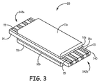
フィードスルー組立体10のトレース15は、基板14の端部142a、142bに延在可能である。この方法では、トレース15は、例えばIMD内に存在する対応する受信部スロット(不図示)と係合するためのカード端部接続部として利用可能である。様々な実施形態では、接触パッド150は、トレース15の一部として含まれる。接触パッド150は、トレース15より大きい表面領域を有することが可能であり、その結果、IMDのトレースと関連する回路との間の陽的な結合が確実にされることが可能である。様々な実施形態では、トレース15/接触パッド150は、端部142a、142bの周りに延在可能であり、図3に示されるように、基板14の端部面140上に存在可能である。端部面140上のトレース15の存在は、接触パッド150があろうとなかろうと、フィードスルー組立体10と、IMD内の受信部スロットとの間の更に一定の結合を提供可能である。
The
次に図4を参照すれば、フィードスルー組立体20は、本開示の様々な実施形態に従った統合型トランシーバ26と共に示される。上記したフィードスルー組立体10と同様、フィードスルー組立体20は、複数の層を含む。基板24は、基板24の一方の側又は両側に形成された複数のトレース25を含む。基板24は、任意の非導電性材料、例えば高温同時焼成セラミックスや他のセラミックス材料で製作可能である。トレース25は、白金や金、パラジウム等の導電性材料を基板24の表面上に被覆することで基板24上に形成可能であり、その結果、基板の一方の端部から他方に延在する。トレース25を形成する他の方法も利用可能である。トレース25は、基板24の第1面244a及び/又は第2面244b上に形成可能である。トレース25は、トレース15及び接触パッド150に関して、上述と同様、接触パッドを含むことが可能である。様々な実施形態では、コンデンサ及び/又はフィルタ機器のような一体型の機器、例えばSAWフィルタは、基板24上に形成され、トレース25に電気的に接続可能である。
Referring now to FIG. 4, the
絶縁層23a、23bは、それぞれ、第1面244a及び第2面244b上に形成可能である。絶縁層は、基板24と同様、高温同時焼成セラミックスや他のセラミックス材料等の任意の非導電性材料で形成可能である。様々な実施形態では、絶縁層23a、23bは、基板24の第1面244a及び第2面244bの一部だけを覆う。基板の端部242a、242bは、露出しているが、絶縁層23a、23bによって覆われない状態にあることが可能である。このやり方で、トレース25は、IMDに電気的に接続可能である。
The insulating layers 23a and 23b can be formed on the
接地面22a、22bは、様々な実施形態で絶縁層23a、23b上に形成可能である。接地面22a、22bは、白金や金、パラジウム等の任意の導電性材料で形成可能である。接地面22a、22bは、トレース25自身の間の干渉を最小化することと同様、トレース25を漂遊電磁干渉から遮蔽することを助ける。様々な実施形態では、接地面22a、22bは、絶縁層23a、23bを覆う絶縁材料の連続層で形成可能である。IMDから接地面22a、22bを絶縁するために、いくつかの実施形態では、他の絶縁層21a、21bは、接地面22a、22b上に形成可能である。上述されるように、接地面22a、22bは、様々な方法で、例えば1又は2以上のトレース25、1又は2以上の接触パッド150、ウェルドリング35(以下に更に充分に記述される)、或いは、それらの結合と接続することで、電気的に接地の電位に接続可能であろう。
The ground planes 22a and 22b can be formed on the insulating layers 23a and 23b in various embodiments. The ground planes 22a and 22b can be formed of any conductive material such as platinum, gold, and palladium. The ground planes 22a, 22b help shield the
フィードスルー組立体20のトレース25は、基板24の端部242a、242bに延在可能である。このやり方で、トレース25は、例えば、IMD内に存在する対応する受信部スロット(不図示)と係合するために、カード端部接続部として、利用可能である。様々な実施形態において、トレース25は、端部242a、242bの周りに延在可能であり、フィードスルー組立体10に関して図3に示されるように、基板24の端部面240上に存在可能である。端部面240上のトレース25の存在は、フィードスルー組立体20とIMDの受信器スロットとの間の更にしっかりした係合を提供可能である。
The
統合型トランシーバ26は、図4内に示されるように、基板24上に搭載された表面であろう。信号イントレース262は、IMDから統合型トランシーバ26に電気的に接続可能である。この方法では、統合型トランシーバ26は、IMDから信号を受信可能である。統合型トランシーバ26は、信号アウトトレース264に更に電気的に接続可能である。信号アウトトレース264は、アンテナに電気的に接続可能であり、或いは、送信/受信要素(不図示)に電気的に接続可能である。この方法では、統合型トランシーバ26は、遠隔機器から情報を受信するのと同様、IMDから受信した情報を遠隔機器に送信可能である。統合型トランシーバ26は、基板24上のトレースとして形成された動力線266によって動力が供給可能である。様々な実施形態では、トランシーバ26は、動力線を含むことが可能であり、及び/又は、ワイヤやリボン結合のような、基板24とその上に形成されたトレース25から離間した信号イン線及び信号アウト線を含むことが可能である。
The
次に図5を参照すれば、本開示の様々な実施形態に従ったフィードスルー組立体30が示される。フィードスルー組立体30は、上述されたフィードスルー組立体10と20に実質的に類似であろう。ウェルドリング35は、フィードスルー組立体30にハーメチックシール可能である。ウェルドリング35は、例えばチタンやニオブ、タンタル、それらの結合体等の任意の生体安定材料及び任意の生体互換性材料で製作可能である。ウェルドリング35は、IMDの本体にも接続可能であり、その結果、IMDとフィードスルー組立体30との間にハーメチックシールがある。ウェルドリング35は、例えば真鍮ジョイントや拡散結合、ガラスシール、圧縮シール等様々なやり方で、フィードスルー組立体に結合可能である。
Referring now to FIG. 5, a feedthrough assembly 30 is shown according to various embodiments of the present disclosure. The feedthrough assembly 30 will be substantially similar to the
次に図6と図7を参照すれば、本開示の様々な実施形態に従ったフィードスルー組立体200が示される。フィードスルー組立体200は、複数の層を含む。基板204は、基板204の一方の側又は両側に形成された複数のトレース205(図7)を含む。基板204は、例えば高温同時焼成セラミックス又は他のセラミックス材料等の任意の非導電性材料で製作可能である。トレース205は、白金、金、パラジム等の導電性材料を基板204の表面上に蒸着することで、基板204上に形成可能である。トレース205を形成する他の方法が利用可能である。
With reference now to FIGS. 6 and 7, a
トレース205は、基板204の第1面244a及び/又は第2面244b上に形成可能である。様々な実施形態において、コンデンサ及び/又はフィルタ機器等の統合型の機器、例えばSAWフィルタは、(例えばスクリーニングやフォトリソグラフィ工程によって)基板204上に形成可能であり、或いは、基板204に適用可能であり、トレース205/接触パッド250に電気的に接続可能である。例えば、SAWフィルタは、リチウムニオブ酸塩やリチウムタンタル酸塩等の様々な材料で、基板204に搭載された表面に製造可能である。この場合、以下に記述される絶縁層は、ハーメチック筐体として機能するために、SAWフィルタを取り囲むことが可能である。
The
絶縁層203a、203bは、それぞれ、第1面244a及び第2面244b上に形成可能である。絶縁層は、基板204に類似して、例えば高温同時焼成セラミックスや他のセラミックス材料等の任意の非導電性材料で形成可能である。いくつかの実施形態では、絶縁層203a、203bは、例えばアルミナやジルコニア、それらの結合体等の任意の生体安定性材料及び任意の生体互換性材料で形成可能である。様々な実施形態では、絶縁層203a、203bは、基板204の第1面244a及び第2面244b全体を覆う。
The insulating
接地面202a、202bは、様々な実施形態において、絶縁層203a、203b上に形成可能である。接地面202a、202bは、例えば白金や金、パラジウム、他の金属等の任意の導電性材料で形成可能である。接地面202a、202bは、トレース205それ自身の間の干渉を最小化するのと同様、漂遊電磁干渉からトレース205を遮蔽するのを助ける。様々な実施形態では、接地面202a、202bは、絶縁層203a、203bを覆う導電性材料の連続層で形成可能である。いくつかの実施形態では、接地面202a、202bは、絶縁層203a、203bを覆う導電性材料の網目又は格子で形成可能である。他の絶縁層201a、201bは、IMDから接地面202a、202bを絶縁するための接地面202a、202b上に形成可能である。示された実施形態は、接地面202a、202bが基板204から離間した層上に形成されるように示すが、本開示は、異なる構成における接地面202a、202bの構成を達成する。例えば、接地面202a、202bは、基板204上に形成可能であり、トレース205から電気的に絶縁可能である。更に、接地面202a、202bは、基板204を実質的に取り囲むように形成可能であり、及び/又は、基板204の第1面244a及び第2面244bに垂直に方向付けられることが可能である。上述されたように、接地面202a、202bは、例えば1又は2以上のトレース205や1又は2以上の接触パッド、ウェルドリング235(以下に更に充分に記述される)、それらの結合体等、様々な方法で、電気的に接地の電位に接続可能である。
The ground planes 202a, 202b can be formed on the insulating
様々な実施形態において、フィードスルー組立体200のトレース205は、基板204の端部に延在しない。替わって、接触パッド250は、別個の層(示された例の絶縁層201a)上に形成され、トレース205と電気的に結合される。このやり方で、接触パッド250は、例えばIMD内に存在する対応する受信部スロット(不図示)と係合するために、カード端部接続部として利用可能である。接触パッド250は、トレース205より大きな表面を有することが可能であり、その結果、トレースとIMDの関連する回路との間の陽的な結合は、確実なものとすることが可能である。様々な実施形態において、接触パッド250は、図3に示されたフィードスルー組立体20に類似して、フィードスルー組立体の端部の周りに延在可能である。端部面上の接触パッド250の存在は、フィードスルー組立体200とIMDの受信部スロットとの間の更にしっかりとした結合を提供可能である。
In various embodiments, the
トレース205は、ビア255を介して接触パッド250と電気的に結合可能である。ビア255は、フィードスルー組立体200の様々な層の間を延在し、白金や金、パラジウムや他の金属などの任意の導電性材料で形成可能である。示された実施形態では、ビア255は、絶縁層201aと接地面202a、絶縁層203aを通じて延在し、接触パッド250をトレース205に結合する。ビア255を接地面202aから絶縁するために、孔257は、ビア255がその中を延在する接地面202a内に形成される。いくつかの実施形態において、孔257は、絶縁材料で充填可能である。他の様々な実施形態において、孔257は、ビア255がその中を延在する様々な層内に空洞の開口部であろう。
本開示の様々な実施形態において、フィードスルー組立体200は、ウェルドリング235を含み、フィードスルー組立体200をハーメチックシールする。ウェルドリング235はまた、IMDの本体に結合可能であり、その結果、IMDとフィードスルー組立体200との間にハーメチックシールがある。ウェルドリング235は、例えば真鍮ジョイントや拡散結合、ガラスシール、圧縮シール等様々なやり方で、フィードスルー組立体に結合可能である。更に、様々な実施形態において、フィードスルー組立体200は、上述し図4に示したフィードスルー組立体20に類似して、統合型トランシーバを含むことが可能である。
In various embodiments of the present disclosure, the
本開示の幅広い教示は、様々な形態で実行可能である。それゆえに、この開示は特殊な例を含むが、図面、明細書、以下の特許請求の範囲を検討すれば他の修正案が明らかになるであろうから、本開示の真の範囲はあまり限定されるべきではない。
〔態様1〕
移植可能な医療器具のための、第1端部及び第2端部を含む多層フィードスルーであって、
前記フィードスルーの前記第1端部に対応する第1端部と、当該フィードスルーの前記第2端部に対応する第2端部と、基板長さと、第1面と、当該第1面とは反対の第2面と、を有する基板と、
前記第1面上に形成され、前記基板長さに沿って延在する、第1の複数のトレースと、
前記第2面上に形成され、前記基板長さに沿って延在する、第2の複数のトレースと、
前記第1の複数のトレースと電気的に結合された第1の複数の接触パッドと、
前記第2の複数のトレースと電気的に結合された第2の複数の接触パッドと、
前記第1面と前記第1の複数のトレースとの上に形成された第1絶縁層と、
前記第2面と前記第2の複数のトレースとの上に形成された第2絶縁層と、
第1接地面層と、
第2接地面層と、
を備え、
前記第1の複数の接触パッド及び第2の複数の接触パッドは、前記フィードスルーの前記第1端部及び前記第2端部に延在する、多層フィードスルー。
〔態様2〕
態様1に記載の多層フィードスルーにおいて、
前記基板の前記第1面上に形成された統合型トランシーバを更に備える、多層フィードスルー。
〔態様3〕
態様2に記載の多層フィードスルーにおいて、
前記第1の複数のトレースは、前記統合型トランシーバのための少なくとも1つの動力線と少なくとも1つの信号線とを含む、多層フィードスルー。
〔態様4〕
態様3に記載の多層フィードスルーにおいて、
前記第1の複数の接触パッド及び前記第2の複数の接触パッドは、前記基板の前記第1端部及び前記第2端部の周りを延在する、多層フィードスルー。
〔態様5〕
態様1に記載の多層フィードスルーにおいて、
前記第1接地面層上に形成された第3絶縁層と、前記第2接地面層上に形成された第4絶縁層とを更に備える、多層フィードスルー。
〔態様6〕
態様5に記載の多層フィードスルーにおいて、
前記第1の複数の接触パッド及び前記第2の複数の接触パッドは、それぞれ、前記第3絶縁層及び第4絶縁層上に形成された、多層フィードスルー。
〔態様7〕
態様6に記載の多層フィードスルーにおいて、
第1の複数のビアは、前記第1の複数の接触パッドを前記第1の複数のトレースに電気的に結合し、
第2の複数のビアは、前記第2の複数の接触パッドを前記第2の複数のトレースに電気的に結合する、多層フィードスルー。
〔態様8〕
態様1に記載の多層フィードスルーにおいて、
前記第1の接地面層は、導電性材料の連続層を備える、多層フィードスルー。
〔態様9〕
態様1に記載の多層フィードスルーにおいて、
前記第1の接地面層は、導電性材料の網目を備える、多層フィードスルー。
〔態様10〕
態様1に記載の多層フィードスルーにおいて、
前記基板と前記第1絶縁層と前記第2絶縁層とは、非導電性材料を備える、多層フィードスルー。
〔態様11〕
態様10に記載の多層フィードスルーにおいて、
前記非導電性材料は、高温同時焼成セラミックスを備える、多層フィードスルー。
〔態様12〕
態様1に記載の多層フィードスルーにおいて、
前記基板は、前記第1端部の直近の第1端部部分と、前記第2端部に直近の第2端部部分とを更に含み、
前記第1絶縁層及び前記第2絶縁層は、前記第1端部部分及び前記第2端部部分に存在しない、多層フィードスルー。
〔態様13〕
態様1に記載の多層フィードスルーにおいて、
前記第1接地面及び前記第2接地面は、前記第1面及び前記第2面に実質的に垂直である、多層フィードスルー。
〔態様14〕
態様1に記載の多層フィードスルーにおいて、
前記第1の複数の接触パッド及び前記第2の複数の接触パッドは、前記基板上に形成された、多層フィードスルー。
〔態様15〕
態様1の多層フィードスルーを備えた移植可能な医療機器。
〔態様16〕
態様1に記載の多層フィードスルーにおいて、
前記第1接地面層は、前記第1の複数のトレースの1つに電気的に接続する、多層フィードスルー。
The broad teachings of the disclosure can be implemented in a variety of forms. Therefore, although this disclosure includes special examples, the true scope of this disclosure is not so limited as other modifications will become apparent after studying the drawings, the specification, and the following claims. Should not be done.
[Aspect 1]
A multi-layer feedthrough including a first end and a second end for an implantable medical device comprising:
A first end corresponding to the first end of the feedthrough, a second end corresponding to the second end of the feedthrough, a substrate length, a first surface, and the first surface; A substrate having an opposite second surface, and
A first plurality of traces formed on the first surface and extending along the substrate length;
A second plurality of traces formed on the second surface and extending along the substrate length;
A first plurality of contact pads electrically coupled to the first plurality of traces;
A second plurality of contact pads electrically coupled to the second plurality of traces;
A first insulating layer formed on the first surface and the first plurality of traces;
A second insulating layer formed on the second surface and the second plurality of traces;
A first ground plane layer;
A second ground plane layer;
With
The first plurality of contact pads and the second plurality of contact pads extend to the first end and the second end of the feedthrough.
[Aspect 2]
In the multilayer feedthrough according to aspect 1,
The multilayer feedthrough further comprising an integrated transceiver formed on the first side of the substrate.
[Aspect 3]
In the multilayer feedthrough according to aspect 2,
The first plurality of traces includes a multilayer feedthrough including at least one power line and at least one signal line for the integrated transceiver.
[Aspect 4]
In the multilayer feedthrough according to aspect 3,
The first plurality of contact pads and the second plurality of contact pads extend around the first end and the second end of the substrate.
[Aspect 5]
In the multilayer feedthrough according to aspect 1,
A multilayer feedthrough further comprising a third insulating layer formed on the first ground plane layer and a fourth insulating layer formed on the second ground plane layer.
[Aspect 6]
In the multilayer feedthrough according to aspect 5,
The first plurality of contact pads and the second plurality of contact pads are multilayer feedthroughs formed on the third insulating layer and the fourth insulating layer, respectively.
[Aspect 7]
In the multilayer feedthrough according to aspect 6,
A first plurality of vias electrically coupling the first plurality of contact pads to the first plurality of traces;
The second plurality of vias electrically couples the second plurality of contact pads to the second plurality of traces.
[Aspect 8]
In the multilayer feedthrough according to aspect 1,
The first ground plane layer comprises a multi-layer feedthrough comprising a continuous layer of conductive material.
[Aspect 9]
In the multilayer feedthrough according to aspect 1,
The first ground plane layer is a multilayer feedthrough comprising a mesh of conductive material.
[Aspect 10]
In the multilayer feedthrough according to aspect 1,
The substrate, the first insulating layer, and the second insulating layer are multilayer feedthroughs comprising a non-conductive material.
[Aspect 11]
In the multilayer feedthrough according to
The non-conductive material is a multilayer feedthrough comprising high temperature co-fired ceramics.
[Aspect 12]
In the multilayer feedthrough according to aspect 1,
The substrate further includes a first end portion proximate to the first end and a second end portion proximate to the second end;
The first insulating layer and the second insulating layer are multilayer feedthroughs that are not present in the first end portion and the second end portion.
[Aspect 13]
In the multilayer feedthrough according to aspect 1,
The multilayer feedthrough, wherein the first ground plane and the second ground plane are substantially perpendicular to the first plane and the second plane.
[Aspect 14]
In the multilayer feedthrough according to aspect 1,
The first plurality of contact pads and the second plurality of contact pads are multi-layer feedthroughs formed on the substrate.
[Aspect 15]
An implantable medical device comprising the multilayer feedthrough of aspect 1.
[Aspect 16]
In the multilayer feedthrough according to aspect 1,
The first ground plane layer is a multi-layer feedthrough that electrically connects to one of the first plurality of traces.
10:フィードスルー組立体、11a,11b:他の絶縁層、12a,12b:接地面、13a,13b:絶縁層、14:基板、15:トレース、35:ウェルドリング、140:端部面、142a,142b:基板の端部、144a:第1面、144b:第2面、150:接触パッド
20:フィードスルー組立体、21a,21b:他の絶縁層、22a,22b:接地面、23a,23b:絶縁層、24:基板、25:トレース、26:統合型トランシーバ、240:端部面、242a,242b:端部、244a:第1面、244b:第2面、262:信号イントレース、264:信号アウトトレース、266:動力線
30:フィードスルー組立体、35:ウェルドリング
200:フィードスルー組立体、201a,201b:他の絶縁層、202a,202b:接地面、203a,203b:絶縁層、204:基板、205:トレース、235:ウェルドリング、250:接触パッド、255:ビア、257:孔
10: Feed-through assembly, 11a, 11b: Other insulating layer, 12a, 12b: Ground plane, 13a, 13b: Insulating layer, 14: Substrate, 15: Trace, 35: Weld ring, 140: End surface,
Claims (2)
高温同時焼成セラミックスで製作され、前記フィードスルーの前記第1端部に対応する第1端部と、当該フィードスルーの前記第2端部に対応する第2端部と、基板長さと、第1面と、当該第1面とは反対の第2面と、を有する基板と、
前記第1面上に形成され、前記基板長さに沿って延在する、第1の複数のトレースと、
前記第2面上に形成され、前記基板長さに沿って延在する、第2の複数のトレースと、
前記第1の複数のトレースと電気的に結合された第1の複数の接触パッドと、
前記第2の複数のトレースと電気的に結合された第2の複数の接触パッドと、
前記第1面と前記第1の複数のトレースとの上に形成された第1絶縁層と、
前記第2面と前記第2の複数のトレースとの上に形成された第2絶縁層と、
前記第1絶縁層上に形成された第1接地面層と、
前記第2絶縁層上に形成された第2接地面層と、
生体安定性と生体適合性を有する材料で形成され、前記第1接地面層上に形成された第3絶縁層と、
生体安定性と生体適合性を有する材料で形成され、前記第2接地面層上に形成された第4絶縁層と、
を備え、
前記基板の前記第1面上に、少なくともスクリーニング工程とフォトリソグラフィ工程のいずれかで形成された、少なくともコンデンサ及びフィルタ機器のいずれかを含む統合型機器を更に備え、
前記第3絶縁層及び第4絶縁層は、前記統合型機器を囲んで前記多層フィードスルーのハーメチック筐体として機能し、
前記第1の複数の接触パッド及び第2の複数の接触パッドは、前記フィードスルーの前記第1端部及び前記第2端部に延在する、多層フィードスルー。 A multi-layer feedthrough including a first end and a second end for an implantable medical device comprising:
A first end corresponding to the first end of the feedthrough, a second end corresponding to the second end of the feedthrough, a substrate length, a first A substrate having a surface and a second surface opposite to the first surface;
A first plurality of traces formed on the first surface and extending along the substrate length;
A second plurality of traces formed on the second surface and extending along the substrate length;
A first plurality of contact pads electrically coupled to the first plurality of traces;
A second plurality of contact pads electrically coupled to the second plurality of traces;
A first insulating layer formed on the first surface and the first plurality of traces;
A second insulating layer formed on the second surface and the second plurality of traces;
A first ground plane layer formed on the first insulating layer;
A second ground plane layer formed on the second insulating layer;
A third insulating layer formed of a material having biostability and biocompatibility and formed on the first ground plane layer;
A fourth insulating layer formed of a material having biostability and biocompatibility and formed on the second ground plane layer;
With
An integrated device including at least one of a capacitor and a filter device formed on at least one of a screening process and a photolithography process on the first surface of the substrate;
The third insulating layer and the fourth insulating layer surround the integrated device and function as a hermetic casing of the multilayer feedthrough,
The first plurality of contact pads and the second plurality of contact pads extend to the first end and the second end of the feedthrough.
前記第1の複数のトレースは、前記統合型機器のための少なくとも1つの動力線と少なくとも1つの信号線とを含む、多層フィードスルー。 The multilayer feedthrough of claim 1,
The first plurality of traces includes a multilayer feedthrough including at least one power line and at least one signal line for the integrated device .
Applications Claiming Priority (3)
| Application Number | Priority Date | Filing Date | Title |
|---|---|---|---|
| US12/608,443 | 2009-10-29 | ||
| US12/608,443 US8373075B2 (en) | 2009-10-29 | 2009-10-29 | Implantable co-fired electrical feedthroughs |
| PCT/US2010/053905 WO2011059682A1 (en) | 2009-10-29 | 2010-10-25 | Implantable co-fired electrical feedthroughs |
Publications (3)
| Publication Number | Publication Date |
|---|---|
| JP2013509247A JP2013509247A (en) | 2013-03-14 |
| JP2013509247A5 JP2013509247A5 (en) | 2013-11-14 |
| JP5788888B2 true JP5788888B2 (en) | 2015-10-07 |
Family
ID=43432172
Family Applications (1)
| Application Number | Title | Priority Date | Filing Date |
|---|---|---|---|
| JP2012536917A Active JP5788888B2 (en) | 2009-10-29 | 2010-10-25 | Implantable co-fired electrical feedthrough |
Country Status (5)
| Country | Link |
|---|---|
| US (1) | US8373075B2 (en) |
| EP (1) | EP2470264B1 (en) |
| JP (1) | JP5788888B2 (en) |
| CN (1) | CN102481454B (en) |
| WO (1) | WO2011059682A1 (en) |
Families Citing this family (23)
| Publication number | Priority date | Publication date | Assignee | Title |
|---|---|---|---|---|
| US11198014B2 (en) | 2011-03-01 | 2021-12-14 | Greatbatch Ltd. | Hermetically sealed filtered feedthrough assembly having a capacitor with an oxide resistant electrical connection to an active implantable medical device housing |
| US8694102B2 (en) * | 2011-03-09 | 2014-04-08 | Greatbatch Ltd. | Ionizing radiation-protected active implantable medical device |
| US8644002B2 (en) | 2011-05-31 | 2014-02-04 | Medtronic, Inc. | Capacitor including registration feature for aligning an insulator layer |
| US9538637B2 (en) * | 2011-06-29 | 2017-01-03 | Finisar Corporation | Multichannel RF feedthroughs |
| US20130058004A1 (en) | 2011-09-01 | 2013-03-07 | Medtronic, Inc. | Feedthrough assembly including underfill access channel and electrically insulating material |
| US8644936B2 (en) | 2012-01-09 | 2014-02-04 | Medtronic, Inc. | Feedthrough assembly including electrical ground through feedthrough substrate |
| EP2617461B1 (en) | 2012-01-16 | 2018-12-19 | Greatbatch Ltd. | Co-fired hermetically sealed feedthrough with alumina substrate and platinum filled via for an active implantable medical device |
| US10420949B2 (en) | 2012-01-16 | 2019-09-24 | Greatbatch Ltd. | Method of manufacturing a feedthrough insulator for an active implantable medical device incorporating a post conductive paste filled pressing step |
| US8649869B2 (en) | 2012-03-05 | 2014-02-11 | Pacesetter, Inc. | Implantable medical device having feedthru assembly with header side bunched conductor array and can side linear conductor array |
| WO2013172846A1 (en) * | 2012-05-17 | 2013-11-21 | Micro Motion, Inc. | Flameproof electrical feed -through |
| US9819129B2 (en) | 2013-10-04 | 2017-11-14 | Western Digital Technologies, Inc. | Hard disk drive with feedthrough connector |
| US9387332B2 (en) | 2013-10-08 | 2016-07-12 | Medtronic, Inc. | Implantable medical devices having hollow sleeve cofire ceramic structures and methods of fabricating the same |
| WO2015108051A1 (en) * | 2014-01-17 | 2015-07-23 | 株式会社村田製作所 | Laminated wiring board and inspection device provided with same |
| US9196303B2 (en) * | 2014-03-06 | 2015-11-24 | HGST Netherlands, B.V. | Feedthrough connector for hermetically sealed electronic devices |
| US9431759B2 (en) | 2014-10-20 | 2016-08-30 | HGST Netherlands B.V. | Feedthrough connector for hermetically sealed electronic devices |
| JP6752135B2 (en) * | 2016-12-19 | 2020-09-09 | マイクロ モーション インコーポレイテッド | Flameproof electric feedthrough |
| EP3449973B1 (en) | 2017-08-30 | 2022-12-21 | Greatbatch Ltd. | Hermetically sealed filtered feedthrough assembly |
| JP2018049015A (en) * | 2017-09-26 | 2018-03-29 | マイクロ モーション インコーポレイテッド | Flameproof electrical feed-through |
| US11896835B2 (en) * | 2017-10-25 | 2024-02-13 | Cochlear Limited | Electrical shielding in implantable medical devices |
| US10918874B2 (en) * | 2018-06-28 | 2021-02-16 | Medtronic, Inc. | Sealed package and method of forming same |
| GB2600950A (en) * | 2020-11-12 | 2022-05-18 | Continental Automotive Gmbh | Electronic assembly and method of producing the same |
| WO2022225517A1 (en) * | 2021-04-21 | 2022-10-27 | Kyocera International, Inc. | Ceramic feedthrough assemblies for electronic devices with metal housings |
| US11424053B1 (en) | 2021-04-21 | 2022-08-23 | Kyocera International, Inc. | Ceramic feedthrough assemblies for electronic devices with metal housings |
Family Cites Families (22)
| Publication number | Priority date | Publication date | Assignee | Title |
|---|---|---|---|---|
| KR910004079A (en) * | 1989-07-21 | 1991-02-28 | 빈센트 조렙 로너 | Improved hybrid microelectronic circuit and manufacturing method thereof |
| US5132648A (en) | 1990-06-08 | 1992-07-21 | Rockwell International Corporation | Large array MMIC feedthrough |
| WO1995034342A1 (en) * | 1994-06-16 | 1995-12-21 | Medtronic, Inc. | Implantable ceramic device enclosure |
| US5782891A (en) | 1994-06-16 | 1998-07-21 | Medtronic, Inc. | Implantable ceramic enclosure for pacing, neurological, and other medical applications in the human body |
| US5620476A (en) | 1995-11-13 | 1997-04-15 | Pacesetter, Inc. | Implantable medical device having shielded and filtered feedthrough assembly and methods for making such assembly |
| US6020562A (en) * | 1997-11-11 | 2000-02-01 | 3Com Corporation | Reduced-capacitance component mounting pads and capacitance-reduction methods for high frequency multi-layer printed circuit boards |
| JPH11195444A (en) * | 1997-12-26 | 1999-07-21 | Amp Japan Ltd | Coaxial cable terminating structure |
| US6052623A (en) | 1998-11-30 | 2000-04-18 | Medtronic, Inc. | Feedthrough assembly for implantable medical devices and methods for providing same |
| US6414835B1 (en) | 2000-03-01 | 2002-07-02 | Medtronic, Inc. | Capacitive filtered feedthrough array for an implantable medical device |
| JP3976020B2 (en) * | 2004-02-12 | 2007-09-12 | 株式会社豊田自動織機 | Surface mounting structure of electronic components for surface mounting |
| US7493167B2 (en) * | 2005-03-22 | 2009-02-17 | Greatbatch-Sierra, Inc. | Magnetically shielded AIMD housing with window for magnetically actuated switch |
| US20070060969A1 (en) | 2005-09-15 | 2007-03-15 | Burdon Jeremy W | Implantable co-fired electrical feedthroughs |
| US7068491B1 (en) | 2005-09-15 | 2006-06-27 | Medtronic, Inc. | Implantable co-fired electrical interconnect systems and devices and methods of fabrication therefor |
| WO2007117302A2 (en) | 2005-11-11 | 2007-10-18 | Greatbatch Ltd. | Low loss band pass filter for rf distance telemetry pin antennas of active implantable medical devices |
| US8160707B2 (en) | 2006-01-30 | 2012-04-17 | Medtronic, Inc. | Method and apparatus for minimizing EMI coupling in a feedthrough array having at least one unfiltered feedthrough |
| US7725190B2 (en) | 2006-01-30 | 2010-05-25 | Medtronic, Inc. | Implantable medical device feedthrough assembly including flange plate |
| US20070203530A1 (en) | 2006-02-28 | 2007-08-30 | Hubing Roger L | Filtered multipolar feedthrough assembly |
| US7668597B2 (en) | 2006-03-31 | 2010-02-23 | Medtronic, Inc. | Feedthrough array for use in implantable medical devices |
| US7746661B2 (en) * | 2006-06-08 | 2010-06-29 | Sandisk Corporation | Printed circuit board with coextensive electrical connectors and contact pad areas |
| DE102006054249A1 (en) | 2006-11-17 | 2008-05-21 | Biotronik Crm Patent Ag | Filter feedthrough for implants |
| CN102037528A (en) * | 2008-03-20 | 2011-04-27 | 格瑞巴奇有限公司 | Shielded three-terminal flat-through EMI/energy dissipating filter |
| US8626310B2 (en) | 2008-12-31 | 2014-01-07 | Medtronic, Inc. | External RF telemetry module for implantable medical devices |
-
2009
- 2009-10-29 US US12/608,443 patent/US8373075B2/en active Active
-
2010
- 2010-10-25 WO PCT/US2010/053905 patent/WO2011059682A1/en active Application Filing
- 2010-10-25 CN CN201080037306.4A patent/CN102481454B/en active Active
- 2010-10-25 JP JP2012536917A patent/JP5788888B2/en active Active
- 2010-10-25 EP EP10774089.6A patent/EP2470264B1/en active Active
Also Published As
| Publication number | Publication date |
|---|---|
| WO2011059682A1 (en) | 2011-05-19 |
| US20110102967A1 (en) | 2011-05-05 |
| CN102481454B (en) | 2014-09-03 |
| CN102481454A (en) | 2012-05-30 |
| EP2470264B1 (en) | 2015-12-23 |
| JP2013509247A (en) | 2013-03-14 |
| EP2470264A1 (en) | 2012-07-04 |
| US8373075B2 (en) | 2013-02-12 |
Similar Documents
| Publication | Publication Date | Title |
|---|---|---|
| JP5788888B2 (en) | Implantable co-fired electrical feedthrough | |
| USRE48348E1 (en) | Feedthrough filter capacitor assembly with internally grounded hermetic insulator | |
| US7046499B1 (en) | Internally grounded filtering feedthrough | |
| US5782891A (en) | Implantable ceramic enclosure for pacing, neurological, and other medical applications in the human body | |
| US10306748B2 (en) | Filtered feedthrough assembly for implantable medical electronic devices | |
| US7035077B2 (en) | Device to protect an active implantable medical device feedthrough capacitor from stray laser weld strikes, and related manufacturing process | |
| US7136273B2 (en) | Hybrid spring contact system for EMI filtered hermetic seals for active implantable medical devices | |
| US8676321B2 (en) | Connection housing and manufacture of same | |
| US9463329B2 (en) | Shielded three-terminal flat-through EMI/energy dissipating filter with co-fired hermetically sealed feedthrough | |
| US8843215B2 (en) | Connecting device | |
| US20070203530A1 (en) | Filtered multipolar feedthrough assembly | |
| WO2008103166A1 (en) | Filtered multipolar feedthrough assembly | |
| US20150283374A1 (en) | Electric Feedthrough For Electromedical Implants, Electric Contact Element Comprising Such A Feedthrough, And Electromedical Implant | |
| US20110094768A1 (en) | Implantable medical device having feedthru with an integrated interconnect/filter substrate | |
| US7590450B2 (en) | Filtered electrical interconnect assembly | |
| US8331077B2 (en) | Capacitor for filtered feedthrough with annular member |
Legal Events
| Date | Code | Title | Description |
|---|---|---|---|
| A521 | Request for written amendment filed |
Free format text: JAPANESE INTERMEDIATE CODE: A523 Effective date: 20130925 |
|
| A621 | Written request for application examination |
Free format text: JAPANESE INTERMEDIATE CODE: A621 Effective date: 20130925 |
|
| A977 | Report on retrieval |
Free format text: JAPANESE INTERMEDIATE CODE: A971007 Effective date: 20140626 |
|
| A131 | Notification of reasons for refusal |
Free format text: JAPANESE INTERMEDIATE CODE: A131 Effective date: 20140714 |
|
| A521 | Request for written amendment filed |
Free format text: JAPANESE INTERMEDIATE CODE: A523 Effective date: 20140828 |
|
| A131 | Notification of reasons for refusal |
Free format text: JAPANESE INTERMEDIATE CODE: A131 Effective date: 20150120 |
|
| A521 | Request for written amendment filed |
Free format text: JAPANESE INTERMEDIATE CODE: A523 Effective date: 20150219 |
|
| TRDD | Decision of grant or rejection written | ||
| A01 | Written decision to grant a patent or to grant a registration (utility model) |
Free format text: JAPANESE INTERMEDIATE CODE: A01 Effective date: 20150701 |
|
| A61 | First payment of annual fees (during grant procedure) |
Free format text: JAPANESE INTERMEDIATE CODE: A61 Effective date: 20150730 |
|
| R150 | Certificate of patent or registration of utility model |
Ref document number: 5788888 Country of ref document: JP Free format text: JAPANESE INTERMEDIATE CODE: R150 |
|
| R250 | Receipt of annual fees |
Free format text: JAPANESE INTERMEDIATE CODE: R250 |
|
| R250 | Receipt of annual fees |
Free format text: JAPANESE INTERMEDIATE CODE: R250 |
|
| R250 | Receipt of annual fees |
Free format text: JAPANESE INTERMEDIATE CODE: R250 |
|
| R250 | Receipt of annual fees |
Free format text: JAPANESE INTERMEDIATE CODE: R250 |
|
| R250 | Receipt of annual fees |
Free format text: JAPANESE INTERMEDIATE CODE: R250 |
|
| R250 | Receipt of annual fees |
Free format text: JAPANESE INTERMEDIATE CODE: R250 |