JP5773071B2 - Antenna device - Google Patents
Antenna device Download PDFInfo
- Publication number
- JP5773071B2 JP5773071B2 JP2014509069A JP2014509069A JP5773071B2 JP 5773071 B2 JP5773071 B2 JP 5773071B2 JP 2014509069 A JP2014509069 A JP 2014509069A JP 2014509069 A JP2014509069 A JP 2014509069A JP 5773071 B2 JP5773071 B2 JP 5773071B2
- Authority
- JP
- Japan
- Prior art keywords
- substrate
- conductive film
- reflector
- edge
- point
- Prior art date
- Legal status (The legal status is an assumption and is not a legal conclusion. Google has not performed a legal analysis and makes no representation as to the accuracy of the status listed.)
- Expired - Fee Related
Links
Images


Classifications
-
- H—ELECTRICITY
- H01—ELECTRIC ELEMENTS
- H01Q—ANTENNAS, i.e. RADIO AERIALS
- H01Q19/00—Combinations of primary active antenna elements and units with secondary devices, e.g. with quasi-optical devices, for giving the antenna a desired directional characteristic
- H01Q19/10—Combinations of primary active antenna elements and units with secondary devices, e.g. with quasi-optical devices, for giving the antenna a desired directional characteristic using reflecting surfaces
- H01Q19/18—Combinations of primary active antenna elements and units with secondary devices, e.g. with quasi-optical devices, for giving the antenna a desired directional characteristic using reflecting surfaces having two or more spaced reflecting surfaces
- H01Q19/185—Combinations of primary active antenna elements and units with secondary devices, e.g. with quasi-optical devices, for giving the antenna a desired directional characteristic using reflecting surfaces having two or more spaced reflecting surfaces wherein the surfaces are plane
-
- H—ELECTRICITY
- H01—ELECTRIC ELEMENTS
- H01Q—ANTENNAS, i.e. RADIO AERIALS
- H01Q9/00—Electrically-short antennas having dimensions not more than twice the operating wavelength and consisting of conductive active radiating elements
- H01Q9/04—Resonant antennas
- H01Q9/16—Resonant antennas with feed intermediate between the extremities of the antenna, e.g. centre-fed dipole
- H01Q9/26—Resonant antennas with feed intermediate between the extremities of the antenna, e.g. centre-fed dipole with folded element or elements, the folded parts being spaced apart a small fraction of operating wavelength
-
- H—ELECTRICITY
- H01—ELECTRIC ELEMENTS
- H01Q—ANTENNAS, i.e. RADIO AERIALS
- H01Q13/00—Waveguide horns or mouths; Slot antennas; Leaky-waveguide antennas; Equivalent structures causing radiation along the transmission path of a guided wave
- H01Q13/10—Resonant slot antennas
-
- H—ELECTRICITY
- H01—ELECTRIC ELEMENTS
- H01Q—ANTENNAS, i.e. RADIO AERIALS
- H01Q19/00—Combinations of primary active antenna elements and units with secondary devices, e.g. with quasi-optical devices, for giving the antenna a desired directional characteristic
- H01Q19/10—Combinations of primary active antenna elements and units with secondary devices, e.g. with quasi-optical devices, for giving the antenna a desired directional characteristic using reflecting surfaces
-
- H—ELECTRICITY
- H01—ELECTRIC ELEMENTS
- H01Q—ANTENNAS, i.e. RADIO AERIALS
- H01Q21/00—Antenna arrays or systems
- H01Q21/06—Arrays of individually energised antenna units similarly polarised and spaced apart
- H01Q21/20—Arrays of individually energised antenna units similarly polarised and spaced apart the units being spaced along or adjacent to a curvilinear path
- H01Q21/205—Arrays of individually energised antenna units similarly polarised and spaced apart the units being spaced along or adjacent to a curvilinear path providing an omnidirectional coverage
Description
本発明は、誘電体板系形成した導電膜に切り込みを設けたアンテナ装置に関する。 The present invention relates to an antenna device in which a cut is provided in a conductive film formed with a dielectric plate.
特許文献1に、加工コスト及びアンテナ重量を低減することができるアンテナ装置が開示されている。このアンテナ装置は、反射板の中央部の前方に配置されたダイポールアンテナを含む。反射板は、両側部に折り返し部を備えている。
特許文献2に、水平放射ビーム幅を広範囲に可変設定可能なアンテナ装置が開示されている。このアンテナ装置は、地導体板の上に、誘電体層及び放射素子が積層された構造を有する。さらに、地導体板の下面の両側部に、地導体板から所定距離に設けられたリフレクタを備えている。
特許文献3に、無指向性に近い放射パターンを持つアンテナ装置が開示されている。このアンテナ装置においては、第1の導体板の給電点に内蔵アンテナが取り付けられている。内蔵アンテナが配置される面とは異なる側の第1の導体板上に、第2の導体板が設けられている。第2の導体板は、1つの辺(接地辺)において第1の導体板に接地される。
本発明の目的は、小型化に適し、指向性を高めることが可能なアンテナ装置を提供することである。 An object of the present invention is to provide an antenna device that is suitable for downsizing and can enhance directivity.
本発明の一観点によると、
誘電体板、及び前記誘電体板の両面に形成された導電膜を含む基板と、
前記基板の両面の前記導電膜に形成され、前記基板の第1の縁の一部分から内側に向かう第1の切り込みと、
前記第1の切り込みの外周線上の第1の点において、前記導電膜に接続された第1の放射電極と、
前記第1の縁から前記基板の内側に向かって、前記第1の点よりも遠い位置に配置され、前記導電膜に電気的に接続され、前記第1の点の方を向く導電性の第1の反射板と
を有し、
前記導電膜は、
前記第1の切り込みから、前記第1の縁に沿って相互に反対向きに伸びる第1の導電部分と、
前記第1の縁から見て、前記第1の導電部分よりも内奥部に配置された第2の導電部分と
を含み、前記第1の導電部分と前記第2の導電部分との間に間隙が設けられており、
前記第1の反射板は、前記第2の導電部分に電気的に短絡されているアンテナ装置が提供される。
第1の反射板が、第1の縁近傍から放射される電磁波の指向性を高める。導電膜を、第1の導電部分と第2の導電部分とに分離すると、放射強度の前後比(F/B比)が高まる。
According to one aspect of the invention,
A substrate including a dielectric plate and a conductive film formed on both surfaces of the dielectric plate;
A first notch formed in the conductive film on both surfaces of the substrate and directed inward from a portion of the first edge of the substrate;
A first radiation electrode connected to the conductive film at a first point on an outer peripheral line of the first cut;
A conductive second electrode disposed at a position farther from the first point from the first edge toward the inside of the substrate, electrically connected to the conductive film, and facing toward the first point. possess and one of the reflector,
The conductive film
First conductive portions extending from the first cut in opposite directions along the first edge; and
A second conductive portion disposed in an inner part of the first conductive portion as viewed from the first edge; and
A gap is provided between the first conductive portion and the second conductive portion,
An antenna device is provided in which the first reflector is electrically short-circuited to the second conductive portion .
The first reflector increases the directivity of the electromagnetic wave radiated from the vicinity of the first edge. When the conductive film is separated into the first conductive portion and the second conductive portion, the front-to-back ratio (F / B ratio) of the radiation intensity increases.
前記第1の反射板を、前記基板に対して垂直な姿勢で、前記基板に取り付けてもよい。
さらに、前記第1の縁から前記基板の内側に向かって、前記第1の反射板よりも遠い領域の、前記基板に高周波回路を配置してもよい。このとき、前記第1の放射電極は、第1の伝送線路により前記高周波回路に接続される。第1の伝送線路は、前記第1の反射板が配置された仮想平面を交差し、かつ前記第1の反射板とは電気的に絶縁されている。
前記第1の反射板は、前記基板の両面に配置してもよい。前記基板を基準として、前記第1の反射板の高さは、前記基板の両面で異なる構成としてもよい。これにより、指向性を、基板の面内方向から厚さ方向に傾けることができる。The first reflecting plate may be attached to the substrate in a posture perpendicular to the substrate.
Furthermore, a high-frequency circuit may be disposed on the substrate in a region farther than the first reflecting plate from the first edge toward the inside of the substrate. At this time, the first radiation electrode is connected to the high-frequency circuit by a first transmission line. The first transmission line intersects an imaginary plane on which the first reflecting plate is disposed, and is electrically insulated from the first reflecting plate.
The first reflector may be disposed on both sides of the substrate. The height of the first reflecting plate may be different on both surfaces of the substrate with respect to the substrate. Thereby, directivity can be inclined from the in-plane direction of the substrate to the thickness direction.
前記基板は、多角形の平面形状を有する構成としてもよい。前記第1の縁は、前記多角形の1つの辺に対応する。さらに、前記多角形の他の辺に対応する前記基板の少なくとも1つの第2の縁の一部分から内側に向かって、前記導電膜に形成された第2の切り込みと、前記第2の切り込みの外周線上の第2の点において、前記導電膜に接続された第2の放射電極と、前記第2の縁から見て、前記第2の点よりも遠い位置に配置され、前記導電膜に電気的に接続され、前記第2の点の方を向く導電性の第2の反射板とを設けてもよい。
これにより、基板の面内方向の複数の方位において、放射電界強度が高まる。The substrate may have a polygonal planar shape. The first edge corresponds to one side of the polygon. Further, a second cut formed in the conductive film inward from a part of at least one second edge of the substrate corresponding to the other side of the polygon, and an outer periphery of the second cut A second radiation electrode connected to the conductive film at a second point on the line and a position farther from the second point when viewed from the second edge, and electrically connected to the conductive film And a conductive second reflector that faces the second point.
Thereby, the radiation electric field intensity increases in a plurality of directions in the in-plane direction of the substrate.
第1の反射板を設けることにより、放射強度の指向性を高めることができる。基板を、第1の導電部分と第2の導電部分とに分離することにより、放射強度の前後比を高めることができる。第1の反射板を基板の両面に配置し、基板の両面で異なる高さとすることにより、指向性を、基板の面内から厚さ方向に傾けることができる。基板を多角形とし、導電膜の各辺に対応する位置に切り込み等を設けることにより、複数の方位において、放射電界強度を高めることができる。 By providing the first reflector, the directivity of the radiation intensity can be increased. By separating the substrate into the first conductive portion and the second conductive portion, the front-to-back ratio of the radiation intensity can be increased. Directivity can be inclined in the thickness direction from the plane of the substrate by disposing the first reflecting plate on both sides of the substrate and having different heights on both sides of the substrate. By making the substrate polygonal and providing cuts or the like at positions corresponding to the respective sides of the conductive film, the radiation electric field strength can be increased in a plurality of directions.
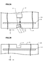
図1Aに、実施例1によるアンテナ装置の概略斜視図を示す。ほぼ正方形状の基板20の1つの縁21の一部分、例えば中央部分に切り込み23が設けられている。基板20は、後述するように、誘電体板と、その両面に形成された導電膜とを含む。切り込み23は、導電膜に形成される。切り込みは、導電膜にのみ形成してもよいし、誘電体板と導電膜との両方に形成してもよい。縁21に平行な方向をy方向、基板20の中心から縁21に向かう方向をx方向、基板20に垂直な方向をz方向とするxyz直交座標系を定義する。
FIG. 1A is a schematic perspective view of the antenna device according to the first embodiment. A
切り込み23は、縁21から基板20の内側(x軸の負の方向)に向かう。放射電極24が、切り込み23の外周線上の第1の点25において、基板20の導電膜に接続されている。切り込み23の一方の側(y軸の正の側)の導電膜と、他方の側(y軸の負の側)の導電膜との間に電位差が与えられる。一例として、同軸ケーブルの外部導体と中心導体とが、それぞれ切り込み23の相互に反対側の縁に接続される。中心導体が接続される第1の点25を接地点(ショート点)という。外部導体が接続された位置からショート点25までの露出した中心導体が、放射電極24に相当する。放射電極24は、放射電極の一部を構成する。露出した中心導体の、ショート点25とは反対側の端部を給電点28という。x方向の正の方向を「前方」といい、負の方向を「後方」ということとする。
The
縁21から基板20の内側(x軸の負の方向)に向かって、切り込み23の先端(縁21から基板20の内側に向かって、最も深い点)よりも遠い位置に反射板26が配置されている。反射板26は、基板20の導電膜に電気的に接続されており、ショート点25の方(x軸の正の方向)を向く姿勢で、基板20に固定されている。例えば、反射板26は、縁21に平行で、かつ基板20に対して垂直(yz面に平行)である。このアンテナ装置は、xy面内に関して、前方の放射強度が最大になる指向特性を有する。
A
さらに、縁21から基板20の内側に向かって、反射板26より遠い位置に、高周波回路30が搭載されている。高周波回路30は、放射電極24に高周波電力を供給する。
Further, a
図1Aでは、反射板26が基板20の両面に配置された例を示しているが、一方の面にのみ反射板26を配置してもよい。また、図1Aでは、縁21から基板20の内側に向かって切り込み23の先端よりも遠い位置に、反射板26を配置したが、反射板26を配置する位置は、ショート点25より遠い位置であればよい。
Although FIG. 1A shows an example in which the
図1Bに、基板20及び反射板26の断面図を示す。基板20は、誘電体板20A、上側導電膜20B、下側導電膜20C、及び貫通ビア20Dを含む。上側導電膜20B及び下側導電膜20Cは、それぞれ誘電体板20Aの上面及び下面に配置されている。貫通ビア20Dは、誘電体板20Aに形成された貫通孔内に配置され、上側導電膜20Bと下側導電膜20Cとを電気的に接続する。誘電体板20A、上側導電膜20B、下側導電膜20C、及び貫通ビア20Dは、アンテナ装置の動作周波数帯域において、1枚の導体板と考えることができる。なお、切り込み23(図1A)の箇所においては、上側導電膜20B及び下側導電膜20Cに切り込みが設けられており、誘電体板20Aには切り込みは形成されていない。切り込み23の部分に誘電体板20Aが残されているが、電気的には、1枚の導体板に切り込み23が形成されている構造と等価である。
FIG. 1B shows a cross-sectional view of the
上側及び下側の反射板26は、銅板等の金属板で形成されており、1つの縁がL字状に折り曲げられている。折り曲げ箇所より先端の部分が、ボルトとナット等の締結具27により、基板20に固定されている。締結具27による取り付けに代えて、はんだ等により反射板26を上側導電膜20B及び下側導電膜20Cに固定してもよい。また、反射板26として、金属板に代えて、誘電体板の表面に金属箔を形成した基板を用いてもよい。金属箔として、例えば厚さ1μm〜2μmの銅箔を用いることができる。
The upper and lower reflecting
図2Aに、切り込み23が形成された部分、縁21、及びその周囲の平面図を示す。上側導電膜20Bに、切り込み23が形成されている。上側導電膜20Bの上に、例えば送受信可能な高周波回路30が搭載されている。高周波回路30と切り込み23との間に反射板26が配置されている。切り込み23の内側に配置された放射電極24が、伝送線路37を介して高周波回路30に接続されている。伝送線路37は、反射板26と交差する。また、放射電極24は、切り込み23内に配置された容量性リアクタンス素子31を介して、ショート点25に接続されている。容量性リアクタンス素子31は、切り込み23の実効的な深さを深くする効果を持つ。
FIG. 2A shows a plan view of the portion where the
さらに、放射電極24は、ショート点25とは反対側の、切り込み23の側面に短絡されている。この短絡により、インピーダンス整合を図ることができる。
Further, the
図2Bに、切り込み23が形成された部分、縁21、及びその周囲の底面図を示す。下側導電膜20Cに、切り込み23が形成されている。上側導電膜20Bに形成された切り込み23と、下側導電膜20Cに形成された切り込み23とは、xy面の面内方向に関して重なる。切り込み23の内側には、誘電体板20A(図1B)が残る。切り込み23の最も深い部分よりやや後方に、下側の反射板26が固定されている。
FIG. 2B shows a bottom view of the portion where the
図3A及び図3Bに、それぞれ実施例2によるアンテナ装置の部分平面図及び部分底面図を示す。以下、実施例1との相違点について説明し、同一の構成については説明を省略する。図3A及び図3Bは、それぞれ実施例1の図2A及び図2Bに対応する部分を示している。 3A and 3B are a partial plan view and a partial bottom view of the antenna device according to the second embodiment, respectively. Hereinafter, differences from the first embodiment will be described, and description of the same configuration will be omitted. 3A and 3B show portions corresponding to FIGS. 2A and 2B of the first embodiment, respectively.
図3Aに示すように、実施例2においては、上側導電膜20Bが、分離帯(間隙)34により第1の導電部分32と第2の導電部分33とに分離されている。第1の導電部分32は、切り込み23から、縁21に沿って相互に反対向き(y方向の正及び負の向き)に伸びる。第2の導電部分33は、縁21から見て、第1の導電部分32より内奥部に配置されている。分離帯34は、縁21に対して平行に伸びる部分と、その両端から縁21に向かって直角に伸びる部分とで構成される。縁21に平行に伸びる部分は、切り込み23と反射板26との間に配置されている。反射板26は、第2の導電部分33に、電気的に短絡される。
As shown in FIG. 3A, in Example 2, the upper
切り込み23の内側に配置された放射電極24が、伝送線路37を介して高周波回路30に接続されている。伝送線路37は、第1の導電部分32及び分離帯34と交差した後、反射板26と交差して高周波回路30に向かう。伝送線路37と第1の導電部分32との交差箇所において、両者は相互に絶縁されている。伝送線路37は、第2の導電部分33が配置された領域内に進入する。伝送線路37が配置された領域には、伝送線路37と第2の導電部分33との絶縁を確保するために、伝送線路37よりも広いスリットが形成されている。伝送線路37は、このスリット内に配置される。伝送線路37と放射電極24との相互接続点が給電点28となる。
The
図3Bに示すように、下側導電膜20Cにも分離帯34が形成されている。分離帯34により、下側導電膜20Cが、第1の導電部分32と第2の導電部分33とに分離されている。ただし、伝送線路37(図3A)と分離帯34との交差箇所に対応する領域の底面に、グランド膜35が配置されている。グランド膜35は、誘電体板20A(図1B)の底面に形成された第1の導電部分32と第2の導電部分33とを接続する。底面側の反射板26も、第2の導電部分33に、電気的に短絡される。
As shown in FIG. 3B, the
図4に、放射電極24、伝送線路37及びその近傍の斜視図を示す。図4においては、図1Bに示した誘電体板20A、上側導電膜20B、下側導電膜20C、及び貫通ビア20Dを、1枚の導体板として表している。伝送線路37及びグランド膜35は、誘電体板20A(図1B)に設けられた貫通ビア20D(図1B)で相互に接続されない。このため、図4において、上側導電膜20B(図1B)と下側導電膜20C(図1B)とを区別して表している。伝送線路37は上側導電膜20Bの一部で構成され、グランド膜35は、下側導電膜20Cの一部で構成される。なお、図4では、反射板26の表示を省略している。
FIG. 4 is a perspective view of the
切り込み23内の領域に配置された放射電極24が、給電点28において、伝送線路37に連続する。伝送線路37は、分離帯34と交差して、第2の導電部分33が配置された領域まで伸びる。伝送線路37と分離帯34との交差箇所に、グランド膜35が配置されている。グランド膜35と伝送線路37とは、マイクロストリップラインを構成する。第2の導電部分33が配置された領域においては、誘電体板20Aの底面に形成された下側導電膜20Cと伝送線路37とが、マイクロストリップラインを構成する。放射電極24と、マイクロストリップライン構造の伝送線路37との境界点が給電点28となる。
The
図5A及び図5Bに、それぞれ図3Aの一点鎖線5A−5A、5B−5Bにおける断面図を示す。誘電体板20Aの上面に、上側導電膜20Bが配置され、底面に下側導電膜20Cが配置されている。上側導電膜20Bによって、放射電極24、伝送線路37及び第2の導電部分33が形成され、下側導電膜20Cによってグランド膜35及び第2の導電部分33が形成される。
5A and 5B are cross-sectional views taken along one-
伝送線路37と反射板26との交差箇所において、両者が接触しないように、反射板26に切り込み36が設けられている。
A
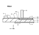
図6に、実施例2の変形例によるアンテナ装置の部分断面図を示す。図6に示した断面図は、図5Aに示した断面図に対応する。以下、図5Aに示した構造との相違点について説明する。 FIG. 6 is a partial cross-sectional view of an antenna device according to a modification of the second embodiment. The cross-sectional view shown in FIG. 6 corresponds to the cross-sectional view shown in FIG. 5A. Hereinafter, differences from the structure shown in FIG. 5A will be described.
図6に示した変形例においては、誘電体板20Aに多層配線基板が用いられる。誘電体板20A内に、伝送線路37の一部31Aが埋め込まれている。埋めこまれた部分31Aは、反射板26と交差する箇所、及び第2の導電部分33と重なる領域に配置される。上側導電膜20Bで形成された伝送線路37と内層の部分37Aとは、導電ビア37Bにより接続される。反射板26との交差箇所で、伝送線路37が誘電体板20Aの内部に配置されるため、伝送線路37と反射板26との絶縁が確保される。第2の導電部分33が配置された領域においては、伝送線路の内層の部分37Aが、上側導電膜20Bと下側導電膜20Cとで挟まれた構造を有する。
In the modification shown in FIG. 6, a multilayer wiring board is used for the
図1A、図5B等では、反射板26の平面形状をほぼ長方形としたが、他の形状でもよい。また、反射板26は、基板20に対して、必ずしも垂直にする必要はない。基板20に対して反射板26を斜めに配置してもよい。また、反射板26の大きさは、前後比の有意な改善が見られる大きさであればよい。
In FIG. 1A, FIG. 5B, etc., the planar shape of the reflecting
次に、図7A〜図9Cを参照して、上記実施例1及び実施例2の効果について説明する。アンテナ装置の各部の寸法を変えて、指向特性をシミュレーションによって算出した。 Next, effects of the first embodiment and the second embodiment will be described with reference to FIGS. 7A to 9C. The directivity was calculated by simulation while changing the dimensions of each part of the antenna device.
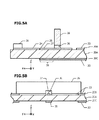
図7A及び図7Bに、それぞれシミュレーションで採用した実施例2によるアンテナ装置の平面図及び部分断面図を示す。基板20の平面形状は、一辺の長さL1が70mmの正方形であり、厚さは1mmである。第1の導電部分32のy方向及びx方向の寸法L2、L3は、それぞれ50mm及び5mmである。分離帯34の幅Wは2.5mmである。放射電極24(図3A)の幅は0.5mmであり、グランド膜35(図3B)の幅は1.1mmである。上側の反射板26の高さをT1とし、下側の反射板26の高さをT2とする。第1の導電部分32のy方向の寸法L2は、動作波長の1/2に設定することが好ましい。
7A and 7B are a plan view and a partial cross-sectional view, respectively, of the antenna device according to the second embodiment employed in the simulation. The planar shape of the
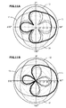
図7Cに、指向特性のシミュレーション結果を示す。中心点が−25dBiに相当し、最外周線が5dBiに相当する。x方向の負の向き(後方)の方位角を0°とし、y方向の正の向きの方位角を90°とした。前方の方位角が180°になる。図7Cにおいて、細い破線a、細い実線b、太い破線cは、それぞれ(T1,T2)=(10mm,10mm)、(15mm,5mm)、(10mm,0mm)の場合のシミュレーション結果を示す。太い実線dは、反射板26を配置しない場合のシミュレーション結果を示す。
FIG. 7C shows a simulation result of directivity characteristics. The center point corresponds to −25 dBi, and the outermost peripheral line corresponds to 5 dBi. The azimuth angle in the negative direction (backward) in the x direction was 0 °, and the azimuth angle in the positive direction in the y direction was 90 °. The front azimuth is 180 °. In FIG. 7C, a thin broken line a, a thin solid line b, and a thick broken line c indicate simulation results when (T1, T2) = (10 mm, 10 mm), (15 mm, 5 mm), and (10 mm, 0 mm), respectively. A thick solid line d indicates a simulation result when the reflecting
反射板26を設けると、後方(方位角0°)への放射が抑制され、かつ前方(方位角180°)への放射が強くなることがわかる。具体的には、(T1,T2)=(10mm,10mm)、(15mm,5mm)、(10mm,0mm)の場合の前後比(F/B比)が、それぞれ10.5dB、10.0dB、8.6dBであった。これに対し、反射板26を設けない場合の前後比は6.9dBであった。このように、反射板26を設けることにより、前方への指向性を高めることができる。
It can be seen that when the
また、図2A及び図2Bに示した実施例1のように、分離帯34を設けない場合でも、反射板26を配置することにより指向性が高まることが確認された。
Further, it was confirmed that the directivity is increased by arranging the
図7A〜図7Cでは、xy面内に関する指向特性について説明した。次に、zx面内に関する指向特性について説明する。 7A to 7C, the directional characteristics related to the xy plane have been described. Next, directivity characteristics regarding the zx plane will be described.
図8Aに示すように、x方向の負の向きを0°とし、z方向の正の向きを90°とする。図8Bに、指向特性のシミュレーション結果を示す。中心点が−5dBiに相当し、最外周線が5dBiに相当する。図8Bにおいて、細い破線a、細い実線b、太い破線cは、それぞれ(T1,T2)=(10mm,10mm)、(15mm,5mm)、(10mm,0mm)の場合のシミュレーション結果を示す。太い実線dは、反射板26を配置しない場合のシミュレーション結果を示す。上下の反射板26の高さが同一である場合(細い破線a)、及び反射板26を配置しない場合(太い実線d)には、角度180°の方向で放射強度が最大となる。上側の反射板26を下側の反射板26より高くした場合(細い実線b)、及び上側にのみ反射板26を配置した場合(太い破線c)には、放射強度が最大になる方向が、角度180°の方向から角度270°の方向(z軸の負の方向)にずれる。
As shown in FIG. 8A, the negative direction in the x direction is 0 °, and the positive direction in the z direction is 90 °. FIG. 8B shows a simulation result of directivity characteristics. The center point corresponds to −5 dBi, and the outermost peripheral line corresponds to 5 dBi. In FIG. 8B, a thin broken line a, a thin solid line b, and a thick broken line c indicate simulation results when (T1, T2) = (10 mm, 10 mm), (15 mm, 5 mm), and (10 mm, 0 mm), respectively. A thick solid line d indicates a simulation result when the reflecting
このように、上下の反射板26の高さを異ならせることにより、放射強度が最大となる方向を、x軸の正の方向から上下方向(z方向)に傾けることができる。上下の反射板26の高さを調節することにより、x軸の正の方向から、放射強度が最大となる方向までの傾き角を変化させることができる。
Thus, by making the heights of the upper and
次に、図9A〜図9Cを参照して、分離帯34(図3A)を設けることの効果について説明する。図9Aは、分離帯34を設けた実施例2によるアンテナ装置の概略平面図を示し、図9Bは、分離帯を設けていない実施例1によるアンテナ装置の概略平面図を示す。
Next, with reference to FIGS. 9A to 9C, the effect of providing the separation band 34 (FIG. 3A) will be described. 9A shows a schematic plan view of the antenna device according to the second embodiment provided with the
図9Cに、図9A及び図9Bに示したアンテナ装置の指向特性のシミュレーション結果を示す。中心点が−25dBiに相当し、最外周線が5dBiに相当する。方位の定義は、図7Cに示した方位の定義と同一である。実線9A及び破線9Bは、それぞれ図9A及び図9Bに示したアンテナ装置のシミュレーション結果を示す。上側の反射板26の高さT1及び下側の反射板26の高さT2を、共に10mmとした。
FIG. 9C shows a simulation result of the directivity of the antenna device shown in FIGS. 9A and 9B. The center point corresponds to −25 dBi, and the outermost peripheral line corresponds to 5 dBi. The definition of the azimuth is the same as the definition of the azimuth shown in FIG. 7C. A
分離帯34を形成すると、後方(x軸の負の方向)への放射強度が低下し、前方(x軸の正の方向)への放射強度が増大することがわかる。具体的には、分離帯34を形成したアンテナ装置(図9A)の前後比が10.5dBであるのに対し、分離帯を形成していないアンテナ装置(図9B)の前後比は、4.3dBである。このように、分離帯34を設けることにより、前後比を高めることができる。
When the
さらに、分離帯34を設けると、高周波回路30(図3A)から第1の導電部分32への雑音の進入を抑制することができる。
次に、図10A〜図12Bを参照して、実施例3によるアンテナ装置について説明する。以下、実施例1及び実施例2との相違点について説明し、同一の構成については説明を省略する。Furthermore, when the
Next, an antenna device according to Example 3 will be described with reference to FIGS. 10A to 12B. Hereinafter, differences from the first embodiment and the second embodiment will be described, and description of the same configuration will be omitted.
実施例1及び実施例2では、図1A等に示したように、四角形の基板20の1つの縁にのみ、切り込み23、放射電極24、反射板26等を含む放射素子が配置されていた。実施例3では、4つの縁に対応して、それぞれ実施例1による放射素子と同一構成の放射素子40が配置されている。図10Aに示したアンテナ装置には、分離帯34(図3A)が設けられておらず、図10Bに示したアンテナ装置の複数の放射素子40に、それぞれ分離帯34が設けられている。
In Example 1 and Example 2, as shown in FIG. 1A and the like, the radiating element including the
図10Cに、図10A及び図10Bに示したアンテナ装置のSパラメータのシミュレーション結果を示す。横軸は周波数を単位「GHz」で表し、縦軸はSパラメータを単位「dB」で表す。図中の破線10Aは、図10Aに示したアンテナ装置のS11、S21パラメータを示し、実線10Bは、図10Bに示したアンテナ装置のS11、S21パラメータを示す。1つの放射素子40へ給電すると、それに隣接する放射素子40から、ある程度の反射がある。S21パラメータは、この入射電力に対する反射電力の比を意味する。
FIG. 10C shows a simulation result of the S parameter of the antenna device shown in FIGS. 10A and 10B. The horizontal axis represents frequency in the unit “GHz”, and the vertical axis represents S parameter in the unit “dB”. A
図10Aに示したアンテナ装置のS21パラメータの最大値が−15dBであるのに対し、図10Bに示したアンテナ装置のS21パラメータの最大値は−18dBである。このシミュレーション結果からわかるように、各放射素子40に分離帯34を設けることにより、放射素子40間の分離性を高めることができる。分離帯34により、放射素子40内に生じる電流分布が、隣接する放射素子40内の電流分布に影響しにくくなるためである。
The maximum value of the S21 parameter of the antenna apparatus shown in FIG. 10A is −15 dB, whereas the maximum value of the S21 parameter of the antenna apparatus shown in FIG. 10B is −18 dB. As can be seen from the simulation results, the separation between the radiating
図10A及び図10Bでは、基板20の平面形状を四角形としたが、四角形以外の多角形としてもよい。例えば、三角形、五角形等の多角形としてもよい。
In FIGS. 10A and 10B, the planar shape of the
図11A及び図11Bに、それぞれ図10A及び図10Bに示したアンテナ装置の指向特性のシミュレーション結果を示す。中心点が−25dBiに相当し、最外周線が5dBiに相当する。図11A及び図11Bの太い実線I1、細い実線I2、太い破線I3、及び細い破線I4は、それぞれ方位角90°、0°、270°、180°の方向を向く放射素子40の放射特性を示す。図10A及び図10Bに示したアンテナ装置のいずれも、放射強度の強い方向が、異なる4方向を向く。
11A and 11B show simulation results of directivity characteristics of the antenna device shown in FIGS. 10A and 10B, respectively. The center point corresponds to −25 dBi, and the outermost peripheral line corresponds to 5 dBi. The thick solid line I1, the thin solid line I2, the thick broken line I3, and the thin broken line I4 in FIGS. 11A and 11B indicate the radiation characteristics of the radiating
1つの放射素子40に着目すると、図10A及び図10Bに示した放射素子40の前後比は、それぞれ7dB及び12dBである。放射素子40の各々の前後比を大きくすることにより、4方向の電界強度を分離して探索することができる。
Focusing on one radiating
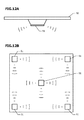
図12A及び図12Bを参照して、実施例3によるアンテナ装置の適用例について説明する。 An application example of the antenna device according to the third embodiment will be described with reference to FIGS. 12A and 12B.
図12Aに示すように、実施例3によるアンテナ装置51が建築物の天井50に取り付けられている。アンテナ装置51の基板20(図10A、図10B)は、ほぼ水平である。鉛直方向に関して、放射強度が最大になる方向が水平方向より下向きになるように、上側及び下側の反射板26(図8A)の高さが調節されている。
As shown to FIG. 12A, the
図12Bに、アンテナ装置51の平面的な配置図を示す。天井に、複数のアンテナ装置51が取り付けられている。各アンテナ装置51の放射素子40(図10A、図10B)によって、電界強度が測定される。各放射素子40で受信された電界強度に基づいて、電波の発信源の位置を絞り込むことができる。床の上で移動する人に発振器を携帯させておくことにより、人の位置を絞り込むことができる。
FIG. 12B shows a planar layout of the
鉛直方向に関して、放射強度が最大になる方向を水平方向より下向きにしておくことにより、床の上を移動する人が携帯する発振器からの電波を効率的に受信することができる。 With respect to the vertical direction, by setting the direction in which the radiation intensity becomes maximum downward from the horizontal direction, it is possible to efficiently receive radio waves from an oscillator carried by a person moving on the floor.
次に、図13A〜図13Dを参照して、ショート点25、給電点28、放射電極24の種々の構成例について説明する。
Next, various configuration examples of the
図13Aに示した給電回路は、図2Aに示した実施例1によるアンテナ装置で用いられている給電回路と等価である。切り込み23の先端の一部に給電点28が位置する。給電点28から伸びる放射電極24がショート点25に接続されている。放射電極24に、容量性リアクタンス素子31が挿入されている。さらに、放射電極24は、ショート点25とは反対側の、切り込み23の縁に、整合用ショート部60(図13A)を介して短絡されている。図13Bに示したように、整合用ショート部60を設けない構成としてもよい。
The feeding circuit shown in FIG. 13A is equivalent to the feeding circuit used in the antenna device according to the first embodiment shown in FIG. 2A. A
図13Cに示すように、切り込み23の一方の縁に給電点28を配置し、それとは反対側の縁にショート点25を設けてもよい。給電点28からショート点25まで放射電極24が伸びる。ショート点25及び給電点28は、切り込み23の開放端の近傍に位置する。図13Dに示すように、ショート点25及び給電点28の位置を、切り込み23の開放端よりも内側にずらしてもよい。このとき、開放端の両側の縁の間に、容量性リアクタンス素子31を挿入してもよい。
As shown in FIG. 13C, a
以上実施例に沿って本発明を説明したが、本発明はこれらに制限されるものではない。例えば、種々の変更、改良、組み合わせ等が可能なことは当業者に自明であろう。 Although the present invention has been described with reference to the embodiments, the present invention is not limited thereto. It will be apparent to those skilled in the art that various modifications, improvements, combinations, and the like can be made.
20 基板
20A 誘電体板
20B 上側導電膜
20C 下側導電膜
20D 貫通ビア
21 縁
23 切り込み
24 放射電極
25 接地点(ショート点)
26 反射板
27 締結具
28 給電点
29 容量性リアクタンス素子
30 高周波回路素子
31 伝送線路(マイクロストリップライン)
37A 内層の伝送線路
37B 導電ビア
32 第1の導電部分
33 第2の導電部分
34 分離帯(間隙)
35 グランド膜
36 切り込み
40 放射素子
50 天井
51 アンテナ装置
60 整合用ショート部20
26
37A Inner
32 First
Claims (6)
前記基板の両面の前記導電膜に形成され、前記基板の第1の縁の一部分から内側に向かう第1の切り込みと、
前記第1の切り込みの外周線上の第1の点において、前記導電膜に接続された第1の放射電極と、
前記第1の縁から前記基板の内側に向かって、前記第1の点よりも遠い位置に配置され、前記導電膜に電気的に接続され、前記第1の点の方を向く導電性の第1の反射板と
を有し、
前記導電膜は、
前記第1の切り込みから、前記第1の縁に沿って相互に反対向きに伸びる第1の導電部分と、
前記第1の縁から見て、前記第1の導電部分よりも内奥部に配置された第2の導電部分と
を含み、前記第1の導電部分と前記第2の導電部分との間に間隙が設けられており、
前記第1の反射板は、前記第2の導電部分に電気的に短絡されているアンテナ装置。 A substrate including a dielectric plate and a conductive film formed on both surfaces of the dielectric plate;
A first notch formed in the conductive film on both surfaces of the substrate and directed inward from a portion of the first edge of the substrate;
A first radiation electrode connected to the conductive film at a first point on an outer peripheral line of the first cut;
A conductive second electrode disposed at a position farther from the first point from the first edge toward the inside of the substrate, electrically connected to the conductive film, and facing toward the first point. possess and one of the reflector,
The conductive film
First conductive portions extending from the first cut in opposite directions along the first edge; and
A second conductive portion disposed in an inner part of the first conductive portion as viewed from the first edge; and
A gap is provided between the first conductive portion and the second conductive portion,
The antenna device, wherein the first reflector is electrically short-circuited to the second conductive portion .
前記基板の両面の前記導電膜に形成され、前記基板の第1の縁の一部分から内側に向かう第1の切り込みと、
前記第1の切り込みの外周線上の第1の点において、前記導電膜に接続された第1の放射電極と、
前記第1の縁から前記基板の内側に向かって、前記第1の点よりも遠い位置に配置され、前記導電膜に電気的に接続され、前記第1の点の方を向く導電性の第1の反射板と、
前記第1の縁から前記基板の内側に向かって、前記第1の反射板よりも遠い領域の、前記基板に配置された高周波回路と、
前記第1の反射板が配置された仮想平面と交差し、かつ前記第1の反射板とは電気的に絶縁されており、前記第1の放射電極を前記高周波回路に接続する第1の伝送線路と
を有するアンテナ装置。 A substrate including a dielectric plate and a conductive film formed on both surfaces of the dielectric plate;
A first notch formed in the conductive film on both surfaces of the substrate and directed inward from a portion of the first edge of the substrate;
A first radiation electrode connected to the conductive film at a first point on an outer peripheral line of the first cut;
A conductive second electrode disposed at a position farther from the first point from the first edge toward the inside of the substrate, electrically connected to the conductive film, and facing toward the first point. 1 reflector,
A high-frequency circuit disposed on the substrate in a region farther than the first reflector from the first edge toward the inside of the substrate;
A first transmission that intersects a virtual plane on which the first reflector is disposed and is electrically insulated from the first reflector, and connects the first radiation electrode to the high-frequency circuit. Rua antenna device having a and the line.
前記第1の縁は、前記多角形の1つの辺に対応し、
さらに、
前記多角形の他の辺に対応する前記基板の少なくとも1つの第2の縁の一部分から内側に向かって、前記導電膜に形成された第2の切り込みと、
前記第2の切り込みの外周線上の第2の点において前記導電膜に接続された第2の放射電極と、
前記第2の縁から見て、前記第2の点よりも遠い位置に配置され、前記導電膜に電気的に接続され、前記第2の点の方を向く導電性の第2の反射板と
を有する請求項1乃至5のいずれか1項に記載のアンテナ装置。
The substrate has a polygonal planar shape;
The first edge corresponds to one side of the polygon;
further,
A second cut formed in the conductive film inwardly from a portion of at least one second edge of the substrate corresponding to the other side of the polygon;
A second radiation electrode connected to the conductive film at a second point on an outer peripheral line of the second cut;
A conductive second reflector disposed at a position farther from the second point as viewed from the second edge, electrically connected to the conductive film, and facing the second point; antenna device according to any one of claims 1 to 5 having a.
Priority Applications (1)
| Application Number | Priority Date | Filing Date | Title |
|---|---|---|---|
| JP2014509069A JP5773071B2 (en) | 2012-04-02 | 2013-02-07 | Antenna device |
Applications Claiming Priority (4)
| Application Number | Priority Date | Filing Date | Title |
|---|---|---|---|
| JP2012083677 | 2012-04-02 | ||
| JP2012083677 | 2012-04-02 | ||
| JP2014509069A JP5773071B2 (en) | 2012-04-02 | 2013-02-07 | Antenna device |
| PCT/JP2013/052859 WO2013150817A1 (en) | 2012-04-02 | 2013-02-07 | Antenna device |
Publications (2)
| Publication Number | Publication Date |
|---|---|
| JP5773071B2 true JP5773071B2 (en) | 2015-09-02 |
| JPWO2013150817A1 JPWO2013150817A1 (en) | 2015-12-17 |
Family
ID=49300318
Family Applications (1)
| Application Number | Title | Priority Date | Filing Date |
|---|---|---|---|
| JP2014509069A Expired - Fee Related JP5773071B2 (en) | 2012-04-02 | 2013-02-07 | Antenna device |
Country Status (3)
| Country | Link |
|---|---|
| US (1) | US9692138B2 (en) |
| JP (1) | JP5773071B2 (en) |
| WO (1) | WO2013150817A1 (en) |
Families Citing this family (2)
| Publication number | Priority date | Publication date | Assignee | Title |
|---|---|---|---|---|
| JP6426493B2 (en) * | 2015-02-16 | 2018-11-21 | Necプラットフォームズ株式会社 | Antenna structure and electronic device |
| JP2019057832A (en) * | 2017-09-21 | 2019-04-11 | 株式会社フジクラ | Antenna device |
Family Cites Families (13)
| Publication number | Priority date | Publication date | Assignee | Title |
|---|---|---|---|---|
| JP3085524B2 (en) * | 1996-11-18 | 2000-09-11 | 日本電業工作株式会社 | Dipole antenna with reflector |
| WO2001082408A1 (en) * | 2000-04-20 | 2001-11-01 | Mitsubishi Denki Kabushiki Kaisha | Portable radio device |
| JP3433222B2 (en) | 2000-05-10 | 2003-08-04 | 防衛庁技術研究本部長 | Antenna device |
| JP2003115715A (en) | 2001-10-09 | 2003-04-18 | Furukawa Electric Co Ltd:The | Antenna assembly |
| JP2003309428A (en) * | 2002-04-15 | 2003-10-31 | Alps Electric Co Ltd | Circularly polarized wave antenna |
| JP4384102B2 (en) | 2005-09-13 | 2009-12-16 | 株式会社東芝 | Portable radio device and antenna device |
| JP5088689B2 (en) * | 2005-11-18 | 2012-12-05 | 日本電気株式会社 | Slot antenna and portable radio terminal |
| JP4728930B2 (en) * | 2006-02-14 | 2011-07-20 | 株式会社日立国際電気 | Corner reflector antenna with ground plane |
| US20100289713A1 (en) * | 2007-05-16 | 2010-11-18 | Toru Taura | Slot antenna |
| WO2009013817A1 (en) | 2007-07-25 | 2009-01-29 | Fujitsu Limited | Wireless tag |
| DE102007058257A1 (en) * | 2007-11-26 | 2009-05-28 | Pilz Gmbh & Co. Kg | Microwave antenna for wireless networking of automation technology devices |
| JP2010245892A (en) | 2009-04-07 | 2010-10-28 | Hitachi Kokusai Electric Inc | Antenna device |
| CN102570058B (en) * | 2010-12-31 | 2014-11-19 | 光宝电子(广州)有限公司 | Compound multi-antenna system and wireless communication device thereof |
-
2013
- 2013-02-07 JP JP2014509069A patent/JP5773071B2/en not_active Expired - Fee Related
- 2013-02-07 WO PCT/JP2013/052859 patent/WO2013150817A1/en active Application Filing
-
2014
- 2014-08-28 US US14/471,221 patent/US9692138B2/en active Active
Also Published As
| Publication number | Publication date |
|---|---|
| US20140368397A1 (en) | 2014-12-18 |
| JPWO2013150817A1 (en) | 2015-12-17 |
| US9692138B2 (en) | 2017-06-27 |
| WO2013150817A1 (en) | 2013-10-10 |
Similar Documents
| Publication | Publication Date | Title |
|---|---|---|
| CN107078404B (en) | Triple polarized antenna element for signals | |
| JP6132031B2 (en) | Patch antenna | |
| JP6528748B2 (en) | Antenna device | |
| JP5429215B2 (en) | Horizontal radiating antenna | |
| US9444147B2 (en) | Ultra-wide-band (UWB) antenna assembly with at least one director and electromagnetic reflective subassembly and method | |
| US20190302225A1 (en) | Antenna apparatus | |
| JP2015185946A (en) | antenna device | |
| JP5227820B2 (en) | Radar system antenna | |
| JP6606871B2 (en) | Antenna and wireless communication device | |
| JP6809600B2 (en) | High frequency module | |
| JPWO2019220536A1 (en) | Array antenna device and communication device | |
| JP2015111763A (en) | Polarization diversity antenna and radio communication apparatus | |
| WO2015133114A1 (en) | Antenna device, wireless communication device, and electronic device | |
| JP6202281B2 (en) | Antenna device | |
| JP5773071B2 (en) | Antenna device | |
| JP5609772B2 (en) | Wide angle directional antenna | |
| JP2011193345A (en) | Electromagnetic wave reflection plane | |
| JP2020174284A (en) | Antenna device | |
| JP3764289B2 (en) | Microstrip antenna | |
| JP6216267B2 (en) | Antenna unit | |
| JP5704095B2 (en) | Array antenna | |
| JP5864226B2 (en) | Compound antenna | |
| JP6747790B2 (en) | Radar equipment | |
| JP2019519095A5 (en) | ||
| JP3338864B2 (en) | Planar antenna |
Legal Events
| Date | Code | Title | Description |
|---|---|---|---|
| TRDD | Decision of grant or rejection written | ||
| A01 | Written decision to grant a patent or to grant a registration (utility model) |
Free format text: JAPANESE INTERMEDIATE CODE: A01 Effective date: 20150602 |
|
| A61 | First payment of annual fees (during grant procedure) |
Free format text: JAPANESE INTERMEDIATE CODE: A61 Effective date: 20150615 |
|
| R150 | Certificate of patent or registration of utility model |
Ref document number: 5773071 Country of ref document: JP Free format text: JAPANESE INTERMEDIATE CODE: R150 |
|
| LAPS | Cancellation because of no payment of annual fees |