JP5772422B2 - ELECTRONIC DEVICE, ITS MANUFACTURING METHOD, FERRITE MAGNET ELEMENT AND ITS MANUFACTURING METHOD - Google Patents
ELECTRONIC DEVICE, ITS MANUFACTURING METHOD, FERRITE MAGNET ELEMENT AND ITS MANUFACTURING METHOD Download PDFInfo
- Publication number
- JP5772422B2 JP5772422B2 JP2011198474A JP2011198474A JP5772422B2 JP 5772422 B2 JP5772422 B2 JP 5772422B2 JP 2011198474 A JP2011198474 A JP 2011198474A JP 2011198474 A JP2011198474 A JP 2011198474A JP 5772422 B2 JP5772422 B2 JP 5772422B2
- Authority
- JP
- Japan
- Prior art keywords
- ferrite
- body portion
- yoke
- hoop material
- lead frame
- Prior art date
- Legal status (The legal status is an assumption and is not a legal conclusion. Google has not performed a legal analysis and makes no representation as to the accuracy of the status listed.)
- Expired - Fee Related
Links
Images


Description
本発明は、電子素子及びその製造方法、特に、マイクロ波帯で使用されるアイソレータやサーキュレータなどの非可逆回路素子に組み込まれるフェライト・磁石素子及びその製造方法に関する。 The present invention relates to an electronic device and a manufacturing method thereof, and more particularly to a ferrite / magnet device incorporated in a nonreciprocal circuit device such as an isolator or a circulator used in a microwave band and a manufacturing method thereof.
従来、アイソレータなどの非可逆回路素子は、予め定められた特定方向にのみ信号を伝送し、逆方向には伝送しない特性を有している。この特性を利用して、例えば、アイソレータは、携帯電話などの移動体通信機器の送信回路部に使用されている。 Conventionally, nonreciprocal circuit elements such as isolators have a characteristic of transmitting a signal only in a predetermined direction and not transmitting in a reverse direction. Utilizing this characteristic, for example, an isolator is used in a transmission circuit unit of a mobile communication device such as a mobile phone.
この種のアイソレータでは、複数の中心電極をフェライトの主面に配置し、該フェライトに永久磁石から直流磁界を印加することで複数の中心電極を結合させている。この場合、永久磁石から発生する磁束の漏れを極力防止することが望ましく、特許文献1に記載のように、軟鉄などの強磁性体に銀めっきを施した金属製のヨークをフェライトと永久磁石の周囲に配置し、これらを接着剤で一体化していた。
In this type of isolator, a plurality of center electrodes are arranged on the main surface of the ferrite, and a plurality of center electrodes are coupled to the ferrite by applying a direct current magnetic field from a permanent magnet. In this case, it is desirable to prevent the leakage of magnetic flux generated from the permanent magnet as much as possible. As described in
しかし、軟鉄などで作製した金属製のヨークは大型化し、フェライトや永久磁石とは独立した個別品として取り扱う必要があり、回路基板上での組立てなどにも手間がかかり量産性に支障を生じている。 However, metal yokes made of soft iron, etc. are upsized and need to be handled as separate products independent of ferrite and permanent magnets, which can be troublesome for assembly on circuit boards, causing problems in mass production. Yes.
そこで、本発明者らは、ヨークをフープ材にて平面視で四角形状をなす枠状に形成することを検討した。本発明との比較のために描かれた図10に示すように、フープ材にて枠状のヨーク150を形成すると、該ヨーク150とフープ材の基部とを連結するリードフレーム153は、通常、ヨーク150の側面と直交する方向に延在させることになる。リードフレームは素子(フェライト・磁石素子)として完成させる際にフープ材からカットされるが、ヨーク150の側面からのカット代Xが必要となりカット残りが発生してしまう。これにて、素子の外形形状が点線で示す専有面積を持つことになり、大きくなってしまう。
Therefore, the present inventors have studied to form the yoke in a frame shape having a quadrangular shape in plan view with a hoop material. As shown in FIG. 10 drawn for comparison with the present invention, when the frame-
そこで、本発明の目的は、フープ材から形成したヨークなどの枠状体を有する電子素子において、リードフレームのカット残りを極力小さくして、素子の小型化を図ることができ、量産性にも適した電子素子、その製造方法、フェライト・磁石素子及びその製造方法を提供することにある。 Accordingly, an object of the present invention is to reduce the cut remainder of the lead frame as much as possible in an electronic element having a frame body such as a yoke formed from a hoop material, so that the element can be miniaturized and mass production can be achieved. It is an object to provide a suitable electronic device, a manufacturing method thereof, a ferrite / magnet device, and a manufacturing method thereof.
本発明の第1形態である電子素子は、
フープ材から形成した平面視で略四角形状をなす枠体部を素子本体部の側面を囲むように配置した電子素子において、
前記枠体部に、フープ材の基部と連結するリードフレームが、該枠体部の略対角線上に延在されており、かつ、前記枠体部の平面視した角部が円弧状に形成されていること、
を特徴とする。
The electronic device according to the first aspect of the present invention is:
In an electronic element in which a frame body portion having a substantially rectangular shape in a plan view formed from a hoop material is disposed so as to surround the side surface of the element body portion,
A lead frame connected to the base portion of the hoop material is extended on the frame body portion substantially on a diagonal line , and a corner portion in plan view of the frame body portion is formed in an arc shape. to have it,
It is characterized by.
本発明の第2形態である電子素子の製造方法は、
フープ材から形成した平面視で略四角形状をなす枠体部を素子本体部の側面を囲むように配置した電子素子の製造方法において、
フープ材に平面視で略四角形状をなす枠体部を形成するとともに、該枠体部をフープ材の基部と連結するリードフレームを該枠体部の略対角線上に形成する工程と、
前記枠体部に素子本体部を配置して該枠体部と該素子本体部とを一体化する工程と、
前記リードフレームをカットする工程と、
を備えたことを特徴とする。
The method for manufacturing an electronic device according to the second embodiment of the present invention is as follows.
In the method for manufacturing an electronic element in which a frame body portion having a substantially rectangular shape in plan view formed from a hoop material is disposed so as to surround a side surface of the element main body portion.
Forming a frame body portion having a substantially rectangular shape in plan view on the hoop material, and forming a lead frame that connects the frame body portion with a base portion of the hoop material on a substantially diagonal line of the frame body portion;
A step of disposing an element body portion on the frame body portion and integrating the frame body portion and the element body portion;
Cutting the lead frame;
It is provided with.
本発明の第3形態であるフェライト・磁石素子は、
対向した一対の主面を有するフェライトと、
前記フェライトの少なくとも一の主面に配置された中心電極と、
前記フェライトの一対の主面にそれぞれ固着された永久磁石と、
前記永久磁石及び前記フェライトの外周面を囲むように配置された平面視で略四角形状をなす枠状のヨークと、
を備え、
前記ヨークは、フープ材から枠状に形成したものであり、かつ、フープ材の基部と連結するリードフレームが、該ヨークの略対角線上に延在されており、さらに、前記ヨークの平面視した角部が円弧状に形成されていること、
を特徴とする。
The ferrite magnet element which is the third embodiment of the present invention is
A ferrite having a pair of opposed principal surfaces;
A central electrode disposed on at least one main surface of the ferrite;
Permanent magnets respectively fixed to a pair of main surfaces of the ferrite;
A frame-shaped yoke having a substantially quadrangular shape in plan view arranged so as to surround the outer peripheral surfaces of the permanent magnet and the ferrite;
With
The yoke is formed in a frame shape from a hoop material, and a lead frame connected to a base portion of the hoop material extends on a substantially diagonal line of the yoke, and further, the yoke is viewed in plan view. The corner is formed in an arc shape ,
It is characterized by.
本発明の第4形態であるフェライト・磁石素子の製造方法は、
対向した一対の主面を有するフェライトの少なくとも一の主面に中心電極を配置し、該フェライトの一対の主面にそれぞれ永久磁石を固着してなるフェライト・磁石素子の製造方法において、
フェライトを一対の永久磁石で挟着した集合基板を作製する工程と、
前記集合基板を短冊状基板にカットして一単位のフェライト・磁石素子とする工程と、
長尺状のフープ材にて平面視で略四角形状をなす複数の枠状のヨークをリードフレームで連結した状態で形成するとともに、該リードフレームを該ヨークの略対角線上に形成する工程と、
前記ヨークに前記フェライト・磁石素子を配置して該ヨークと該フェライト・磁石素子とを一体化する工程と、
前記リードフレームをカットする工程と、
を備えたことを特徴とする。
The method for producing a ferrite magnet element according to the fourth aspect of the present invention is as follows.
In the method of manufacturing a ferrite magnet element in which a central electrode is disposed on at least one main surface of a ferrite having a pair of opposed main surfaces, and permanent magnets are fixed to the pair of main surfaces of the ferrite, respectively.
Producing a collective substrate sandwiched with a pair of permanent magnets;
Cutting the aggregate substrate into strip-shaped substrates to form a unit of ferrite and magnet elements;
Forming a plurality of frame-shaped yokes having a substantially rectangular shape in plan view with a long hoop material in a state of being connected by a lead frame, and forming the lead frame on a substantially diagonal line of the yoke;
Arranging the ferrite-magnet element on the yoke and integrating the yoke and the ferrite-magnet element;
Cutting the lead frame;
It is provided with.
前記電子素子及び前記フェライト・磁石素子において、平面視で略四角形状をなす枠体部(ヨーク)には、フープ材の基部と連結するリードフレームが、該枠体部(ヨーク)の略対角線上に延在されており、かつ、前記枠体部(ヨーク)の平面視した角部が円弧状に形成されているため、該リードフレームをカットする際のカット代は枠体部(ヨーク)の側面から傾斜した距離に設定すればよく、その分だけ電子素子やフェライト・磁石素子の外形が小さくなる。 In the electronic element and the ferrite / magnet element, a lead frame connected to the base portion of the hoop material is on a substantially diagonal line of the frame body (yoke). Since the corner portion of the frame portion (yoke) in plan view is formed in an arc shape, the cutting margin for cutting the lead frame is that of the frame portion (yoke). What is necessary is just to set to the distance inclined from the side surface, and the external shape of an electronic element or a ferrite magnet element becomes small by that much.
また、枠体部やヨークは電子素子やフェライト・磁石素子の製造工程中に素子本体部やフェライト・磁石素子に組み付けられ、回路基板上での別途組立て工程を必要とすることがなく、量産性が向上する。 In addition, the frame and yoke are assembled to the element body and ferrite / magnet element during the manufacturing process of the electronic element, ferrite / magnet element, and do not require a separate assembly process on the circuit board. Will improve.
本発明によれば、電子素子やフェライト・磁石素子の外形が小さくなり素子の小型化を図ることができる。また、枠状体やヨークを個別品としてではなく、素子本体部やフェライト・磁石素子と一体的に取り扱うことができ、ひいては量産性が向上する。 According to the present invention, the outer dimensions of the electronic element and the ferrite / magnet element are reduced, and the element can be miniaturized. Further, the frame body and the yoke can be handled integrally with the element main body and the ferrite / magnet element, not as individual products, and thus mass productivity is improved.
以下、本発明に係る電子素子、その製造方法、フェライト・磁石素子及びその製造方法の実施例について添付図面を参照して説明する。なお、各図において、同じ部材、部分については共通する符号を付し、重複する説明は省略する。 Embodiments of an electronic device, a manufacturing method thereof, a ferrite / magnet device and a manufacturing method thereof according to the present invention will be described below with reference to the accompanying drawings. In addition, in each figure, the same code | symbol is attached | subjected about the same member and part, and the overlapping description is abbreviate | omitted.
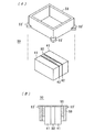
一実施例であるフェライト・磁石素子30は、図1に示すように、非可逆回路素子を構成する一つの素子であり、非可逆回路素子としては、この素子以外に、図示していない回路基板や外装樹脂、必要に応じて実装されるインダクタやコンデンサを含んでいる。なお、フェライト・磁石素子30(非可逆回路素子)としての基本的な構成は従来から種々の態様があり、集中定数型のアイソレータとしては、前述した特許文献1に記載されている2ポート型のアイソレータを挙げることができる。
As shown in FIG. 1, the
この2ポート型のアイソレータ(フェライト・磁石素子30)は、図2に示すように、一対の永久磁石41により直流磁界が印加されるフェライト32と、該フェライト32に互いに絶縁状態で交差して配置された第1中心電極35及び第2中心電極36を備えている。第1中心電極35は、フェライト32に1ターン巻回されており、一端電極35aが入力ポートP1とされ、他端電極35bが出力ポートP2とされている。第2中心電極36は、フェライト32に第1中心電極35と所定の角度で交差した状態で4ターン(ターン数は任意である)巻回されており、一端電極(前記他端電極35bと共用)が出力ポートP2とされ、他端電極36aがグランドポートP3とされている。なお、図2では煩雑さを避けるためにフェライト32の背面側に形成された中心電極は図示を省略している。
As shown in FIG. 2, the two-port isolator (ferrite / magnet element 30) is arranged so that a
さらに、入力ポートP1と出力ポートP2との間に図示しない終端抵抗が第1中心電極35と並列に接続され、入力ポートP1と出力ポートP2との間に、図示しない第1整合用コンデンサが接続され、出力ポートP2とグランドポートP3との間に図示しない第2整合用コンデンサが接続されている。
Further, a termination resistor (not shown) is connected between the input port P1 and the output port P2 in parallel with the
そして、第1及び第2中心電極35,36を設けたフェライト32はその両主面を一対の永久磁石41にて接着剤42を介して挟着されたフェライト・磁石素子30として構成されている。前記終端抵抗や前記コンデンサはフェライト・磁石素子30とは別部品として構成されている。
The
さらに、永久磁石41とフェライト32の外周面に枠状のヨーク50が配置され、ヨーク50の内周面と永久磁石41及びフェライト32の外周面との間に接着剤55が配置されている。ヨーク50は、以下に説明するように磁性体からなるフープ材51(図5参照)を絞り加工又はバーリング加工にて枠状に成形されている。ヨーク50はフープ材51の基部とリードフレーム53にて4隅にて連結され、図1においてはカット残り53’としてヨークに残されている。このリードフレームに関しては後に詳述する。接着剤55としてはエポキシ系樹脂などを素材として好適に用いることができる。ヨーク50は、NiやSPCCなどの磁性体からなり、永久磁石41から発生する磁束の漏れを防止する。
Further, a frame-shaped
ところで、ヨーク50はその下部がフェライト・磁石素子30の下面から若干上方に位置して該下面から浮き上がっている。フェライト・磁石素子30はその下面側が実装面となり、電極35a,35b,36aが図示しない回路基板上の端子電極にはんだ付けされることから、ヨーク50が下部まで延在されていると接合用はんだと短絡するおそれがある。このような短絡を防止するため、ヨーク50は実装面に近い部分から離して配置されている。
By the way, the lower portion of the
ここで、フェライト・磁石素子30の製造工程の要部について図3を参照して説明する。まず、図3(A),(B)に示すように、樹脂製シート60上にヨーク50を配置する。このとき、フープ材51の基部(リードフレーム53)を樹脂製シート60に密着させる。次に、図3(C)に示すように、樹脂製シート60上であってヨーク50の略中央部分に対応する位置に接着剤55をノズル71から適量塗布する。
Here, the principal part of the manufacturing process of the
次に、図3(D)に示すように、フェライト・磁石素子30を上方からヨーク50内に挿入する。このとき、図3(E)に示すように、接着剤55はフェライト・磁石素子30によって押圧されてヨーク50の内周面に沿って押し広げられる。接着剤55を仮硬化させた後、図3(F)に示すように、素子30及びヨーク50を樹脂製シート60から剥離し、図3(G)に示すように、カッタ72にてリードフレーム53をカットする。ここで、リードフレーム53はカット残り53’となる。
Next, as shown in FIG. 3D, the ferrite /
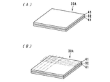
図4には、フェライト・磁石素子30の製造工程を示す。まず、図4(A)に示すように、表面に1単位ごとの中心電極35,36をマトリクス状に形成したフェライト32を永久磁石41で挟着した集合基板30Aを作製する。この集合基板30Aは、例えば、1素子30を縦横に70×30個、計2100個をマトリクス状に形成したものである。
FIG. 4 shows a manufacturing process of the ferrite /
次に、図4(B)に示すように、前記集合基板30Aを一点鎖線に沿って1単位の素子30ごとにカットする。カットは円盤状ダイサーを用いて表裏面から2工程で行われる。このように、1単位に切り出された素子30(1単位の短冊状基板)が図3(D),(E)に示したようにヨーク50に挿入される。
Next, as shown in FIG. 4B, the
また、ヨーク50は、図5に示すように、磁性体からなる長尺状のフープ材51にその長手方向(矢印A方向)に例えば2列に形成される。フープ材51の両側には搬送/位置決め用のパイロット穴52が形成されており、枠状のヨーク50はリードフレーム53によってフープ材51の基部に連結されている。
Further, as shown in FIG. 5, the
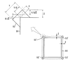
前記リードフレーム53はヨーク50の平面視で4隅部に略対角線上に延在するように形成されている。略対角線上に延在するリードフレーム53を、図10に示したマージンXと同じ量に設定して直線的にカットすると図7に示す形状(第1例)にカットされ、カット残り53’が形成されることになる。カット残り53’を含めたヨーク50の外形増加分Zは、リードフレーム53の延在方向を45°、カットマージンをX、幅寸法をYとすると、Z=(Y/2√2+X/√2)となる。
The
ところで、図7に示す第1例において、カット残り53’の存在によるヨーク50の外形サイズの増加分Zを図10に示した比較例での増加分X(マージンそのもの)より小さくするには、以下の式が成立する必要がある。
(Y/2√2+X/√2)<X
Y<X(2√2−2)
∴Y<0.83X
By the way, in the first example shown in FIG. 7, in order to make the increase amount Z of the outer size of the
(Y / 2√2 + X / √2) <X
Y <X (2√2-2)
∴ Y <0.83X
実際上、カットマージンXは0.05〜0.1mmであるため、前式が成立するにはリードフレーム53の幅寸法Yが0.04〜0.08mmであることが必要となる。しかし、これでは幅寸法Yが小さいので、第1例は実用性に難点がある。
In practice, since the cut margin X is 0.05 to 0.1 mm, the width dimension Y of the
図8は、カット形状の第2例を示す。本第2例では、ヨーク50の4隅部を円弧形状としたもので、略対角線上に延在するリードフレーム53は円弧の接線からマージンXと同じ量に設定して直線的にカットし、カット残り53’を形成した。本第2例では、カットマージンXを円弧の接線から設定するため、カット残り53’の端部は前記第1例と比較するとSだけ内部に平行移動することになり、外形増加分ZはZ’だけ小さくなる。Z’はS/√2に等しい。
FIG. 8 shows a second example of the cut shape. In this second example, the four corners of the
本第2例における、カット残り53’を含めたヨーク50の外形増加分Zは、Z=(Y/2√2+X/√2−S/√2)となり、前記第1例と比較してもS/√2だけ小さくなる。そして、カット残り53’の存在によるヨーク50の外形サイズの増加分Zを図10に示した比較例での増加分X(マージンそのもの)よりも小さくするには、以下の式が成立する必要がある。
(Y/2√2+X/√2−S/√2)<X
Y<X(2√2−2)+2S
∴Y<0.83X+2S
In this second example, the increase in the outer shape Z of the
(Y / 2√2 + X / √2-S / √2) <X
Y <X (2√2-2) + 2S
∴ Y <0.83X + 2S
カットマージンXを0.08mm、リードフレーム53の幅寸法Yを0.16mmとすると、Sは0.05mmであり、幅寸法Yが0.16mmは十分に実現性のある数値である。
When the cut margin X is 0.08 mm and the width dimension Y of the
図9にカット形状の第3例を示す。本第3例では、ヨーク50の4隅部を円弧形状とするとともに、略対角線上に延在するリードフレーム53の端部をも円弧状にカットした。図9における符号72’はカッタ72の内側刃面を示している。本第3例では、前記第2例と比較しても、外形増加分ZはZ”分だけ小さくなる。例えば、ヨーク50の平面形状の縦寸法は1.55mm、横寸法は1.27mm、内側の半径r1は0.1mm、外側の半径r2は0.15mm、カット残り53’の半径r3は0.2mmである。
FIG. 9 shows a third example of the cut shape. In the third example, the four corners of the
次に、フェライト・磁石素子30の全体的な製造工程を模式的に描いた図6を参照して説明する。
Next, the overall manufacturing process of the ferrite /
図6(A)に工程(1)として示すように、上下に配置したローラ81,82の間を搬送されるコンベアベルト61上に、下部に長尺状樹脂製シート60を、上部にヨーク50を形成した長尺状フープ材51を配置して重ねて貼り合わせ、矢印A方向に搬送する。貼り合わせにはローラ81,82を用いたのはあくまで一例であり、他の機構を用いてもよいことは勿論である。次に、工程(2)として、ノズル71から適量の接着剤55を樹脂製シート60上に塗布する。塗布位置は図3(C)に示されている。
As shown as step (1) in FIG. 6A, on the
次に、工程(3)として、前述のごとく短冊状基板として切り出され、かつ、図示しないパーツフィーダに整列された1単位の素子30を図示しないマウンタを用いて各ヨーク50に挿入する(図3(D),(E)参照)。なお、パーツフィーダやマウンタは周知であり、その説明は省略する。次に、工程(4)として、接着剤55を仮硬化させる。接着剤55としてエポキシ系樹脂を使用した場合、仮硬化は、例えば、150℃で30分間加熱することによって行われる。
Next, as step (3), one unit of
次に、工程(5)として、樹脂製シート60から仮硬化した接着剤55を剥がす。即ち、一体化されたヨーク50と素子30を樹脂製シート60から剥離する。さらに、工程(6)として、素子30を台座62上に載置し、カッタ72にてリードフレーム53をカットし、フープ材51から切り離す。さらに、工程(7)として接着剤55を本硬化させる。接着剤55としてエポキシ系樹脂を使用した場合の本硬化は、例えば、150℃で30分間加熱することによって行われる。以上のごとく作製されたフェライト・磁石素子30は、工程(8)として、着磁装置の着磁ヘッド75の間にセットされ、永久磁石41に必要な着磁が行われる。
Next, as the step (5), the temporarily cured adhesive 55 is peeled off from the
フェライト・磁石素子30は、以上のごとく完成された状態で、ヨーク50がフェライト32や永久磁石41と一体化されている。換言すれば、ヨーク50はフェライト・磁石素子30の製造工程中にフェライト・磁石素子30に組み付けられ、別途組立て工程を必要とすることがない。よって、非可逆回路素子の製造工程が簡略化され、量産性が向上する。
In the state where the
なお、本発明は、コンデンサやフィルタ、LC複合素子などの電子素子に適用することも可能である。即ち、フープ材から形成した平面視で略四角形状をなす枠体部を素子本体部の側面を囲むように配置した電子素子において、前記枠体部に、フープ材の基部と連結するリードフレームが、該枠体部の略対角線上に延在されていればよい。リードフレームを適宜マージンを取ってカットすることにより、電子素子の外形を小型化することができる。 The present invention can also be applied to electronic elements such as capacitors, filters, and LC composite elements. That is, in an electronic device in which a substantially rectangular frame body portion formed from a hoop material is disposed so as to surround the side surface of the element body portion, a lead frame connected to the base portion of the hoop material is provided on the frame body portion. It suffices if it extends on a substantially diagonal line of the frame part. By cutting the lead frame with an appropriate margin, the outer shape of the electronic element can be reduced.
また、このような電子素子は、フープ材に平面視で略四角形状をなす枠体部を形成するとともに、該枠体部をフープ材の基部と連結するリードフレームを該枠体部の略対角線上に形成する工程と、前記枠体部に素子本体部を配置して該枠体部と該素子本体部とを一体化する工程と、前記リードフレームをカットする工程と、によって製造することができる。 In addition, such an electronic element has a frame body portion having a substantially square shape in plan view on the hoop material, and a lead frame that connects the frame body portion to the base portion of the hoop material is substantially diagonal to the frame body portion. The manufacturing process includes a step of forming the element body portion on the frame body portion, a step of integrating the frame body portion and the element body portion, and a step of cutting the lead frame. it can.
なお、本発明に係る電子素子、その製造方法、フェライト・磁石素子及びその製造方法は前記実施例に限定するものではなく、その要旨の範囲内で種々に変更することができる。 The electronic device, the manufacturing method thereof, the ferrite / magnet device and the manufacturing method thereof according to the present invention are not limited to the above-described embodiments, and various modifications can be made within the scope of the gist.
例えば、フェライトに形成される中心電極は種々の形態を採用でき、非可逆回路素子としては、実施例として示した2ポート型のアイソレータ以外に、3ポート型、あるいは、磁気共鳴型のアイソレータなどであってもよい。 For example, various forms can be adopted for the center electrode formed on the ferrite, and as the nonreciprocal circuit element, in addition to the 2-port type isolator shown in the embodiment, a 3-port type or magnetic resonance type isolator is used. There may be.
以上のように、本発明は、電子素子、その製造方法、フェライト・磁石素子及びその製造方法に有用であり、特に、リードフレームのカット残りを極力小さくして、素子の小型化を図り、量産性に適している点で優れている。 As described above, the present invention is useful for an electronic device, a manufacturing method thereof, a ferrite / magnet device, and a manufacturing method thereof. In particular, the cutting residue of the lead frame is reduced as much as possible to reduce the size of the device, and to mass production. It is excellent in that it is suitable for sex.
30…フェライト・磁石素子
32…フェライト
35,36…中心電極
41…永久磁石
50…ヨーク(枠体部)
51…フープ材
53…リードフレーム
53’…カット残り
30 ... Ferrite /
51 ...
Claims (8)
前記枠体部に、フープ材の基部と連結するリードフレームが、該枠体部の略対角線上に延在されており、かつ、前記枠体部の平面視した角部が円弧状に形成されていること、
を特徴とする電子素子。 In an electronic element in which a frame body portion having a substantially rectangular shape in a plan view formed from a hoop material is disposed so as to surround the side surface of the element body portion,
A lead frame connected to the base portion of the hoop material is extended on the frame body portion substantially on a diagonal line , and a corner portion in plan view of the frame body portion is formed in an arc shape. to have it,
An electronic device characterized by the above.
フープ材に平面視で略四角形状をなす枠体部を形成するとともに、該枠体部をフープ材の基部と連結するリードフレームを該枠体部の略対角線上に形成する工程と、
前記枠体部に素子本体部を配置して該枠体部と該素子本体部とを一体化する工程と、
前記リードフレームをカットする工程と、
を備えたことを特徴とする電子素子の製造方法。 In the method of manufacturing an electronic element in which a frame body portion having a substantially rectangular shape in a plan view formed from a hoop material is disposed so as to surround a side surface of the element body portion,
Forming a frame body portion having a substantially rectangular shape in plan view on the hoop material, and forming a lead frame that connects the frame body portion with a base portion of the hoop material on a substantially diagonal line of the frame body portion;
A step of disposing an element body portion on the frame body portion and integrating the frame body portion and the element body portion;
Cutting the lead frame;
A method for manufacturing an electronic device, comprising:
前記フェライトの少なくとも一の主面に配置された中心電極と、
前記フェライトの一対の主面にそれぞれ固着された永久磁石と、
前記永久磁石及び前記フェライトの外周面を囲むように配置された平面視で略四角形状をなす枠状のヨークと、
を備え、
前記ヨークは、フープ材から枠状に形成したものであり、かつ、フープ材の基部と連結するリードフレームが、該ヨークの略対角線上に延在されており、さらに、前記ヨークの平面視した角部が円弧状に形成されていること、
を特徴とするフェライト・磁石素子。 A ferrite having a pair of opposed principal surfaces;
A central electrode disposed on at least one main surface of the ferrite;
Permanent magnets respectively fixed to a pair of main surfaces of the ferrite;
A frame-shaped yoke having a substantially quadrangular shape in plan view arranged so as to surround the outer peripheral surfaces of the permanent magnet and the ferrite;
With
The yoke is formed in a frame shape from a hoop material, and a lead frame connected to a base portion of the hoop material extends on a substantially diagonal line of the yoke, and further, the yoke is viewed in plan view. The corner is formed in an arc shape ,
Ferrite / magnet element.
フェライトを一対の永久磁石で挟着した集合基板を作製する工程と、
前記集合基板を短冊状基板にカットして一単位のフェライト・磁石素子とする工程と、
長尺状のフープ材にて平面視で略四角形状をなす複数の枠状のヨークをリードフレームで連結した状態で形成するとともに、該リードフレームを該ヨークの略対角線上に形成する工程と、
前記ヨークに前記フェライト・磁石素子を配置して該ヨークと該フェライト・磁石素子とを一体化する工程と、
前記リードフレームをカットする工程と、
を備えたことを特徴とするフェライト・磁石素子の製造方法。 In the method of manufacturing a ferrite magnet element in which a central electrode is disposed on at least one main surface of a ferrite having a pair of opposed main surfaces, and permanent magnets are fixed to the pair of main surfaces of the ferrite, respectively.
Producing a collective substrate sandwiched with a pair of permanent magnets;
Cutting the aggregate substrate into strip-shaped substrates to form a unit of ferrite and magnet elements;
Forming a plurality of frame-shaped yokes having a substantially rectangular shape in plan view with a long hoop material in a state of being connected by a lead frame, and forming the lead frame on a substantially diagonal line of the yoke;
Arranging the ferrite-magnet element on the yoke and integrating the yoke and the ferrite-magnet element;
Cutting the lead frame;
A method for producing a ferrite / magnet element, comprising:
Priority Applications (1)
| Application Number | Priority Date | Filing Date | Title |
|---|---|---|---|
| JP2011198474A JP5772422B2 (en) | 2011-09-12 | 2011-09-12 | ELECTRONIC DEVICE, ITS MANUFACTURING METHOD, FERRITE MAGNET ELEMENT AND ITS MANUFACTURING METHOD |
Applications Claiming Priority (1)
| Application Number | Priority Date | Filing Date | Title |
|---|---|---|---|
| JP2011198474A JP5772422B2 (en) | 2011-09-12 | 2011-09-12 | ELECTRONIC DEVICE, ITS MANUFACTURING METHOD, FERRITE MAGNET ELEMENT AND ITS MANUFACTURING METHOD |
Publications (2)
| Publication Number | Publication Date |
|---|---|
| JP2013062596A JP2013062596A (en) | 2013-04-04 |
| JP5772422B2 true JP5772422B2 (en) | 2015-09-02 |
Family
ID=48186917
Family Applications (1)
| Application Number | Title | Priority Date | Filing Date |
|---|---|---|---|
| JP2011198474A Expired - Fee Related JP5772422B2 (en) | 2011-09-12 | 2011-09-12 | ELECTRONIC DEVICE, ITS MANUFACTURING METHOD, FERRITE MAGNET ELEMENT AND ITS MANUFACTURING METHOD |
Country Status (1)
| Country | Link |
|---|---|
| JP (1) | JP5772422B2 (en) |
Families Citing this family (1)
| Publication number | Priority date | Publication date | Assignee | Title |
|---|---|---|---|---|
| CN207637968U (en) * | 2017-11-15 | 2018-07-20 | 深圳市华扬通信技术有限公司 | A kind of closed Surface Mount circulator |
Family Cites Families (3)
| Publication number | Priority date | Publication date | Assignee | Title |
|---|---|---|---|---|
| JP2002271110A (en) * | 2001-03-09 | 2002-09-20 | Murata Mfg Co Ltd | Nonreciprocal circuit element and communications equipment |
| JP2006073570A (en) * | 2004-08-31 | 2006-03-16 | Renesas Technology Corp | Semiconductor device and its manufacturing method |
| WO2012132584A1 (en) * | 2011-03-31 | 2012-10-04 | 株式会社村田製作所 | Ferrite/magnet element and method for producing same |
-
2011
- 2011-09-12 JP JP2011198474A patent/JP5772422B2/en not_active Expired - Fee Related
Also Published As
| Publication number | Publication date |
|---|---|
| JP2013062596A (en) | 2013-04-04 |
Similar Documents
| Publication | Publication Date | Title |
|---|---|---|
| JP4380769B2 (en) | Non-reciprocal circuit device, manufacturing method thereof, and communication device | |
| EP2105987B1 (en) | Non-reversible circuit element and method of manufacturing it | |
| JP4656186B2 (en) | Non-reciprocal circuit device and method of manufacturing composite electronic component | |
| JP5018790B2 (en) | Non-reciprocal circuit element | |
| JP5772422B2 (en) | ELECTRONIC DEVICE, ITS MANUFACTURING METHOD, FERRITE MAGNET ELEMENT AND ITS MANUFACTURING METHOD | |
| WO2015029680A1 (en) | Isolator | |
| JP5553130B2 (en) | Ferrite magnet element and manufacturing method thereof | |
| JP5573178B2 (en) | Non-reciprocal circuit element | |
| JP5168011B2 (en) | Non-reciprocal circuit element | |
| JP2012213034A (en) | Ferrite magnet element and manufacturing method therefor | |
| JP4915366B2 (en) | Non-reciprocal circuit element | |
| JP2011147011A (en) | Circuit module | |
| JP5136322B2 (en) | Non-reciprocal circuit element | |
| JP2012119801A (en) | Method of manufacturing non-reciprocal circuit element | |
| US20180115038A1 (en) | Non-reciprocal circuit element, high-frequency circuit and communication device | |
| JP2012165063A (en) | Ferrite magnet element and manufacturing method therefor | |
| JP4807457B2 (en) | Non-reciprocal circuit element | |
| WO2017090304A1 (en) | Non-reversible circuit element, front end circuit and communication device | |
| JP2012138719A (en) | Non-reciprocal circuit element and ferrite magnet element | |
| JP2010081394A (en) | Irreversible circuit element and manufacturing method thereof | |
| WO2017094407A1 (en) | Non-reciprocal circuit element, module circuit, and communication apparatus | |
| JP2012175202A (en) | Ferrite magnet element | |
| JP5652116B2 (en) | Non-reciprocal circuit element | |
| JP2012175201A (en) | Ferrite magnet element | |
| JP2010010804A (en) | Method of manufacturing ferrite magnet element |
Legal Events
| Date | Code | Title | Description |
|---|---|---|---|
| A621 | Written request for application examination |
Free format text: JAPANESE INTERMEDIATE CODE: A621 Effective date: 20140617 |
|
| A977 | Report on retrieval |
Free format text: JAPANESE INTERMEDIATE CODE: A971007 Effective date: 20150227 |
|
| A131 | Notification of reasons for refusal |
Free format text: JAPANESE INTERMEDIATE CODE: A131 Effective date: 20150317 |
|
| A521 | Request for written amendment filed |
Free format text: JAPANESE INTERMEDIATE CODE: A523 Effective date: 20150512 |
|
| RD02 | Notification of acceptance of power of attorney |
Free format text: JAPANESE INTERMEDIATE CODE: A7422 Effective date: 20150512 |
|
| TRDD | Decision of grant or rejection written | ||
| A01 | Written decision to grant a patent or to grant a registration (utility model) |
Free format text: JAPANESE INTERMEDIATE CODE: A01 Effective date: 20150602 |
|
| A61 | First payment of annual fees (during grant procedure) |
Free format text: JAPANESE INTERMEDIATE CODE: A61 Effective date: 20150615 |
|
| R150 | Certificate of patent or registration of utility model |
Ref document number: 5772422 Country of ref document: JP Free format text: JAPANESE INTERMEDIATE CODE: R150 |
|
| LAPS | Cancellation because of no payment of annual fees |