JP5772003B2 - Suspension substrate, method for manufacturing suspension substrate, suspension, suspension with element, and hard disk drive - Google Patents
Suspension substrate, method for manufacturing suspension substrate, suspension, suspension with element, and hard disk drive Download PDFInfo
- Publication number
- JP5772003B2 JP5772003B2 JP2011009958A JP2011009958A JP5772003B2 JP 5772003 B2 JP5772003 B2 JP 5772003B2 JP 2011009958 A JP2011009958 A JP 2011009958A JP 2011009958 A JP2011009958 A JP 2011009958A JP 5772003 B2 JP5772003 B2 JP 5772003B2
- Authority
- JP
- Japan
- Prior art keywords
- layer
- suspension
- wiring layer
- base insulating
- insulating layer
- Prior art date
- Legal status (The legal status is an assumption and is not a legal conclusion. Google has not performed a legal analysis and makes no representation as to the accuracy of the status listed.)
- Expired - Fee Related
Links
Images





Landscapes
- Adjustment Of The Magnetic Head Position Track Following On Tapes (AREA)
Description
本発明は、ビアの設置自由度の高いサスペンション用基板に関するものである。 The present invention relates to a suspension substrate having a high degree of freedom for via installation.
例えば、HDD(ハードディスクドライブ)に用いられる回路基板として、磁気ヘッドスライダ等の素子を実装するサスペンション用基板(フレキシャー)が知られている。サスペンション用基板は、通常、金属支持基板(例えばSUS)、ベース絶縁層(例えばポリイミド樹脂)、配線(例えばCu)等がこの順に積層された基本構造を有し、通常は、一方の先端に、素子を実装する素子実装領域を備え、他方の先端に、外部回路基板と接続を行う外部接続端子領域を備え、両者を上記配線が接続する。 For example, as a circuit board used in an HDD (Hard Disk Drive), a suspension board (flexure) on which elements such as a magnetic head slider are mounted is known. The suspension substrate usually has a basic structure in which a metal support substrate (for example, SUS), a base insulating layer (for example, polyimide resin), a wiring (for example, Cu), and the like are laminated in this order. An element mounting area for mounting elements is provided, and an external connection terminal area for connecting to an external circuit board is provided at the other tip, and the wiring is connected to both.
近年、インターネットの普及等によりパーソナルコンピュータの情報処理量の増大や情報処理速度の高速化が要求されてきており、それに伴って、パーソナルコンピュータに組み込まれているHDDも大容量化や情報伝達速度の高速化が必要となってきている。そのため、HDDに用いられるサスペンション用基板にも高機能化が求められている。 In recent years, due to the spread of the Internet and the like, there has been a demand for an increase in the amount of information processing of personal computers and an increase in information processing speed. Accordingly, HDDs incorporated in personal computers have increased capacity and information transmission speed. Speeding up is needed. For this reason, higher functionality is also demanded for suspension substrates used in HDDs.
その結果、HDDからの読み取り安定性のためにアーム部やリミッタ等種々の部材の追加(例えば、特許文献1)や、サスペンション用基板の小型化により、上記素子実装領域を含むジンバル部内の空き面積、すなわち、上記ベース絶縁層が露出し上記配線やビア等を設置可能な面積が縮小している。
特に、上記ビアは、上記ベース絶縁層に形成されたビア用貫通孔に形成され、上記ビア用貫通孔の周囲を囲むように形成されるビア用配線層と金属支持基板とを接続するものである。ここで、上記ビア用貫通孔の形成方法としては、例えば、上記ベース絶縁層を光硬化性材料を用いて形成する方法が用いられる。このような方法では露光光が上記ベース絶縁層の下部である金属支持基板側まで十分に到達しにくいといった問題や、ウェットエッチングでは微細化が困難であるといった問題があり、上記ビア用貫通孔の断面形状が上記導体層側ほど孔径が大きくなる逆テーパー形状となる。このため、上記ビアと金属支持基板とが十分に接続できるように上記ビア用貫通孔の金属支持基板側の孔径であるビア底部の孔径を所定のサイズとした場合、上記導体層側の孔径が上記ビア底部の孔径よりも大きくなる。
また、上記ビア用貫通孔の周囲を囲むように形成されるビア用配線層の外径も上記導体層側の孔径のサイズに伴い大きくなることから、上記ビアを形成するためには広い設置面積が必要となり、ビアの設置自由度が低くいものとなるといった問題があった。また、このようなことから、近年の空き面積の小さいジンバル部等でのビアの形成が困難となるといった問題があった。
As a result, free space in the gimbal part including the element mounting area is achieved by adding various members such as an arm part and a limiter for stability of reading from the HDD (for example, Patent Document 1) and downsizing the suspension board. That is, the area where the base insulating layer is exposed and the wiring and vias can be installed is reduced.
In particular, the via is formed in a via hole formed in the base insulating layer, and connects the via wiring layer formed so as to surround the via hole and the metal support substrate. is there. Here, as a method for forming the via hole, for example, a method of forming the base insulating layer using a photocurable material is used. In such a method, there is a problem that exposure light does not sufficiently reach the metal support substrate side, which is the lower part of the base insulating layer, and a problem that it is difficult to miniaturize by wet etching. The cross-sectional shape is an inversely tapered shape with the hole diameter increasing toward the conductor layer. Therefore, when the hole diameter at the bottom of the via, which is the hole diameter on the metal support substrate side of the via hole, is set to a predetermined size so that the via and the metal support substrate can be sufficiently connected, the hole diameter on the conductor layer side is It becomes larger than the hole diameter of the via bottom.
In addition, since the outer diameter of the via wiring layer formed so as to surround the via hole is increased with the size of the hole on the conductor layer side, a large installation area is required to form the via. There is a problem that the degree of freedom of via installation is low. In addition, because of this, there has been a problem that it is difficult to form a via in a gimbal portion or the like having a small vacant area in recent years.
本発明は、上記問題点に鑑みてなされたものであり、ビアの設置自由度の高いサスペンション用基板を提供することを主目的とする。 The present invention has been made in view of the above problems, and a main object of the present invention is to provide a suspension substrate having a high degree of freedom of via installation.
上記課題を解決するために、本発明は、金属支持基板と、上記金属支持基板上に形成されたベース絶縁層と、上記ベース絶縁層上に形成された導体層と、を有するサスペンション用基板であって、上記ベース絶縁層が、テーパー角度が45°〜85°の範囲内のビア用貫通孔を有し、上記導体層が、平面視上、上記ビア用貫通孔の周囲を囲むように形成され、外径が40μm〜122μmの範囲内のビア用配線層および上記ビア用配線層に接続された接続配線層を有し、上記ビア用貫通孔内に充填されてなり、上記金属支持基板および上記ビア用配線層を接続する導電性材料からなるビアを有することを特徴とするサスペンション用基板を提供する。 In order to solve the above problems, the present invention provides a suspension substrate having a metal support substrate, a base insulating layer formed on the metal support substrate, and a conductor layer formed on the base insulating layer. The base insulating layer has a through hole for a via having a taper angle of 45 ° to 85 °, and the conductor layer is formed so as to surround the via through hole in a plan view. A via wiring layer having an outer diameter in the range of 40 μm to 122 μm and a connection wiring layer connected to the via wiring layer, the via through hole being filled, and the metal supporting board and A suspension substrate having a via made of a conductive material for connecting the via wiring layer is provided.
本発明によれば、上記ビア用貫通孔のテーパー角度が上述の範囲内であり、上記ビア用配線層の外径が上述の範囲内であることにより、ビアを設置するための面積を小さいものとすることができる。その結果、上記ビアを上記ジンバル部のような空き領域の少ない場所にも容易に形成できる等、ビアの設置自由度の高いものとすることができる。 According to the present invention, the taper angle of the via hole is within the above range, and the outer diameter of the via wiring layer is within the above range, so that the area for installing the via is small. It can be. As a result, the via can be easily formed in a place with a small empty area such as the gimbal portion, and the via can be installed with a high degree of freedom.
本発明においては、上記金属支持基板が、2つのビアと接続され、上記金属支持基板と絶縁されているジャンパー部を有することが好ましい。上記ジャンパー部を有し、2以上のビアが隣接するような場合であっても設置が容易であることから、本発明の効果をより効果的に発揮することができるからである。 In the present invention, it is preferable that the metal support board has a jumper portion connected to two vias and insulated from the metal support board. This is because even if the jumper portion is provided and two or more vias are adjacent to each other, the installation is easy, so that the effect of the present invention can be more effectively exhibited.
本発明においては、上記接続配線層が、リード配線またはライト配線として機能する第1配線層および第2配線層を有し、上記第1配線層および第2配線層が、2以上の分岐配線層を有し、上記第1配線層に属する配線層と、上記第二配線層に属する配線層とが交互に配置されたインターリーブ構造が形成され、上記第1配線層および第2配線層の一方に属する分岐配線層が、上記ビアおよびジャンパー部を介して分岐元の配線層と接続されていることが好ましい。差動インピーダンスを低減させ、消費電力の低いものとすることができるからである。 In the present invention, the connection wiring layer has a first wiring layer and a second wiring layer that function as a read wiring or a write wiring, and the first wiring layer and the second wiring layer include two or more branch wiring layers. An interleaved structure in which wiring layers belonging to the first wiring layer and wiring layers belonging to the second wiring layer are alternately arranged is formed on one of the first wiring layer and the second wiring layer. It is preferable that the branch wiring layer to which the branch belongs is connected to the branch wiring layer via the via and the jumper portion. This is because the differential impedance can be reduced and the power consumption can be reduced.
本発明においては、上記ビアが、上記サスペンション用基板のジンバル部に形成されていることが好ましい。空き面積の小さいジンバル部であっても容易に形成でき、本発明の効果をより効果的に発揮することができるからである。例えば、上述のようにインターリーブ構造が形成されている場合には、交互配線領域を長く形成することができ、差動インピーダンスのさらなる低減を図ることができ、低消費電力化を図ることができるからである。 In the present invention, the via is preferably formed in the gimbal portion of the suspension substrate. This is because even a gimbal portion having a small vacant area can be easily formed, and the effects of the present invention can be exhibited more effectively. For example, when the interleave structure is formed as described above, the alternate wiring region can be formed long, the differential impedance can be further reduced, and the power consumption can be reduced. It is.
本発明においては、上記ベース絶縁層を構成する材料が、ポリイミド成分および感光剤としてクマル酸アミド系光塩基発生剤を含む感光性ポリイミド樹脂組成物を用いてなるベース絶縁層用ポリイミド樹脂であることが好ましい。上記ベース絶縁層が上述の材料からなるものとすることにより上記テーパー角度のビア用貫通孔を有するベース絶縁層を容易に形成できるからである。 In this invention, the material which comprises the said base insulating layer is a polyimide resin for base insulating layers which uses the polyimide component and the photosensitive polyimide resin composition containing a coumaric-amide type photobase generator as a photosensitive agent. Is preferred. This is because, when the base insulating layer is made of the above-mentioned material, the base insulating layer having the via hole having the taper angle can be easily formed.
本発明は、上述のサスペンション用基板を含むことを特徴とするサスペンションを提供する。 The present invention provides a suspension including the above-described suspension substrate.
本発明によれば、上述したサスペンション用基板を用いることで、設計の自由度の高いものとすることができ、例えば、消費電力の低いサスペンションとすることができる。 According to the present invention, by using the suspension substrate described above, it is possible to achieve a high degree of design freedom, for example, a suspension with low power consumption.
また、本発明においては、上述したサスペンションと、上記サスペンションの素子実装領域に実装された素子(例えばスライダ)と、を有することを特徴とする素子付サスペンションを提供する。 According to the present invention, there is provided a suspension with an element characterized by including the above-described suspension and an element (for example, a slider) mounted in an element mounting region of the suspension.
本発明によれば、上述したサスペンションを用いることで、設計の自由度の高いものとすることができ、例えば、消費電力の低い素子付サスペンションとすることができる。 According to the present invention, by using the suspension described above, it is possible to achieve a high degree of design freedom, for example, a suspension with an element with low power consumption.
また、本発明においては、上述した素子付サスペンションを含むことを特徴とするハードディスクドライブを提供する。 The present invention also provides a hard disk drive including the above-described suspension with an element.
本発明によれば、上述した素子付サスペンションを用いることで、より高機能化されたものとすることができ、例えば、消費電力の低いハードディスクドライブとすることができる。 According to the present invention, by using the above-described suspension with an element, it is possible to achieve higher functionality, for example, a hard disk drive with low power consumption.
本発明は、金属支持基板上に形成されたベース絶縁層形成用層をパターニングして、テーパー角度が45°〜85°の範囲内のビア用貫通孔を有するベース絶縁層を形成するベース絶縁層形成工程と、上記ベース絶縁層またはベース絶縁層形成用層上に形成された導体層形成用層をパターニングして、外径が40μm〜122μmの範囲内のビア用配線層および上記ビア用配線層に接続された接続配線層を有する導体層を形成する導体層形成工程と、導電性材料を上記金属支持基板および上記ビア用配線層を接続するように上記ビア用貫通孔に充填しビアを形成するビア形成工程と、を有することを特徴とするサスペンション用基板の製造方法を提供する。 The present invention relates to a base insulating layer for patterning a base insulating layer forming layer formed on a metal supporting substrate to form a base insulating layer having a through-hole for a via having a taper angle of 45 ° to 85 °. Forming via, patterning the base insulating layer or the conductor layer forming layer formed on the base insulating layer forming layer, and a via wiring layer having an outer diameter in a range of 40 μm to 122 μm and the via wiring layer A conductor layer forming step for forming a conductor layer having a connection wiring layer connected to the via hole, and filling the via through hole with a conductive material so as to connect the metal support substrate and the via wiring layer to form a via. There is provided a method for manufacturing a suspension substrate, comprising a via forming step.
本発明によれば、上記範囲内のテーパー角度のビア用貫通孔および外径のビア用配線層を形成することにより、ビアの設置自由度の高いサスペンション用基板を容易に得ることができる。 According to the present invention, by forming a via hole having a taper angle within the above range and a via wiring layer having an outer diameter, a suspension substrate having a high degree of freedom in via installation can be easily obtained.
本発明においては、上記ベース絶縁層形成工程が、上記金属支持基板上にポリイミド成分および感光剤としてクマル酸アミド系光塩基発生剤を含む感光性ポリイミド樹脂組成物を用いて形成されたベース絶縁層形成用層を露光・現像するものであることが好ましい。上記ベース絶縁層を上記材料を用いて形成することにより、上述のテーパー角度のビア用貫通孔を容易に形成することができるからである。また、その結果、上記外径のビア用配線層も容易に形成することができるからである。 In the present invention, the base insulating layer forming step is a base insulating layer formed using a photosensitive polyimide resin composition containing a coumaric acid amide photobase generator as a polyimide component and a photosensitive agent on the metal support substrate. It is preferable to expose and develop the forming layer. This is because by forming the base insulating layer using the material, the via hole having the taper angle can be easily formed. As a result, the via wiring layer having the outer diameter can be easily formed.
本発明においては、上記ベース絶縁層形成工程が、上記金属支持基板上にポリイミド成分を含む非感光性ポリイミド樹脂組成物を用いて形成されたベース絶縁層形成用層上に金属層を形成し、上記金属層をマスクとして上記ベース絶縁層形成用層をエッチングするものであることが好ましい。上述のテーパー角度のビア用貫通孔を容易に形成することができるからである。また、その結果、上記外径のビア用配線層も容易に形成することができるからである。 In the present invention, the base insulating layer forming step forms a metal layer on the base insulating layer forming layer formed using a non-photosensitive polyimide resin composition containing a polyimide component on the metal supporting substrate, The base insulating layer forming layer is preferably etched using the metal layer as a mask. This is because the via hole having the taper angle can be easily formed. As a result, the via wiring layer having the outer diameter can be easily formed.
本発明は、ビアの設置自由度の高いサスペンション用基板を提供できるといった効果を奏する。 The present invention has an effect of providing a suspension substrate having a high degree of freedom for via installation.
本発明は、サスペンション用基板、それを用いたサスペンション、素子付サスペンションおよびハードディスクドライブ、ならびにその製造方法に関するものである。
以下、本発明のサスペンション用基板、サスペンション用基板の製造方法、サスペンション、素子付サスペンションおよびハードディスクドライブについて詳細に説明する。
The present invention relates to a suspension board, a suspension using the same, a suspension with an element and a hard disk drive, and a method of manufacturing the same.
The suspension substrate, suspension substrate manufacturing method, suspension, suspension with element, and hard disk drive of the present invention will be described in detail below.
A.サスペンション用基板
まず、本発明のサスペンション用基板について説明する。
本発明のサスペンション用基板は、金属支持基板と、上記金属支持基板上に形成されたベース絶縁層と、上記ベース絶縁層上に形成された導体層と、を有するサスペンション用基板であって、上記ベース絶縁層が、テーパー角度が45°〜85°の範囲内のビア用貫通孔を有し、上記導体層が、平面視上、上記ビア用貫通孔の周囲を囲むように形成され、外径が40μm〜122μmの範囲内のビア用配線層および上記ビア用配線層に接続された接続配線層を有し、上記ビア用貫通孔内に充填されてなり、上記金属支持基板および上記ビア用配線層を接続する導電性材料からなるビアを有することを特徴とするものである。
A. First, the suspension substrate of the present invention will be described.
The suspension substrate of the present invention is a suspension substrate having a metal support substrate, a base insulating layer formed on the metal support substrate, and a conductor layer formed on the base insulating layer, The insulating base layer has a through-hole for a via having a taper angle of 45 ° to 85 °, and the conductor layer is formed so as to surround the via-through hole in a plan view, and has an outer diameter. Has a via wiring layer in the range of 40 μm to 122 μm and a connection wiring layer connected to the via wiring layer, and is filled in the via through hole, and the metal support substrate and the via wiring It is characterized by having a via made of a conductive material for connecting the layers.
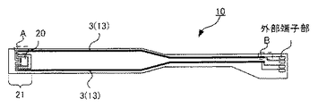
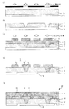
このような本発明のサスペンション用基板について図を参照して説明する。図1は、本発明のサスペンション用基板の一例を示す概略平面図である。図1に示されるサスペンション用基板10は、一方の先端部分に形成された素子実装領域20を含むジンバル部21と、上記素子実装領域20の反対側の端部に配置された外部端子部と、上記外部端子部および素子実装領域20を接続する導体層3(接続配線層13)と、を有するものである。
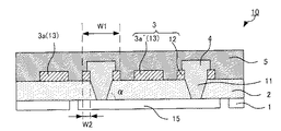
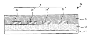
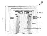
また、図2は、図1のジンバル部21および外部端子領域の近傍(図1中のAおよびB)を示す概略平面図であり、図3は図2の裏面側を示す概略平面図であり、図4および図5は、それぞれ、図2のA−A線断面図およびB−B線断面図である。図1〜図5に例示するように、本発明のサスペンション用基板10は、金属支持基板1と、上記金属支持基板1上に形成されたベース絶縁層2と、上記ベース絶縁層2上に形成された導体層3と、を有するサスペンション用基板であって、上記ベース絶縁層2が、テーパー角度αが74°〜82°の範囲内のビア用貫通孔11を有し、上記導体層3が、平面視上、上記ビア用貫通孔11の周囲を囲むように形成され、外径w1が42μm〜106μmの範囲内のビア用配線層12および上記ビア用配線層12に接続された接続配線層13を有し、上記ビア用貫通孔内11に充填されてなり、上記金属支持基板1および上記ビア用配線層12を接続する導電性材料からなるビア4を有するものである。
Such a suspension substrate of the present invention will be described with reference to the drawings. FIG. 1 is a schematic plan view showing an example of the suspension substrate of the present invention. A
2 is a schematic plan view showing the vicinity (A and B in FIG. 1) of the
また、上記導体層3は、接続配線層13として、リード用配線層またはライト用配線層である第一配線層3aおよび第2配線層3bを有し、上記第1配線層3aおよび第2配線層3bは、それぞれ、分岐配線層(3a´および3b´)を有する。これらの分岐配線層(3a´および3b´)は、上記ジンバル部21内の領域Aおよび外部端子領域内の領域Bで、上記ビア4および上記金属支持基板1の一部であるジャンパー部15により再度分岐元である上記第1配線層3aまたは第2配線層3bに接続されている。すなわち、上記第1配線層3aに属する分岐配線層3a´は、上記ビア4およびジャンパー部15を介して第2配線層3bの分岐配線層3b´の下方を通過し、分岐元の第1配線層3aに接続され、上記第2配線層3bに属する分岐配線層3b´は、上記ビア4およびジャンパー部15を介して第1配線層3aに属する分岐配線層3a´の下方を通過し、分岐元の第2配線層3bに接続されている。また、上記第1配線層3aに属する配線層(3a、3a´)と、上記第2配線層に属する配線層(3b、3b´)とは、交互に配置され、インターリーブ構造が形成されている。
さらに、上記導体層3およびビア4を覆うようにカバー層5が形成されている。
なお、図1および図2においては、説明の容易のため、カバー層の記載を省略するものである。
The
Further, a
In FIGS. 1 and 2, the cover layer is not shown for ease of explanation.
本発明によれば、上記ビア用貫通孔のテーパー角度が上述の範囲内であり、上記ビア用配線層の外径が上述の範囲内であることにより、ビアを設置するための面積を小さいものとすることができる。その結果、上記ビアを上記ジンバル部のような空き領域の少ない場所にも容易に形成できる等、ビアの設置自由度の高いものとすることができる。 According to the present invention, the taper angle of the via hole is within the above range, and the outer diameter of the via wiring layer is within the above range, so that the area for installing the via is small. It can be. As a result, the via can be easily formed in a place with a small empty area such as the gimbal portion, and the via can be installed with a high degree of freedom.
このため、例えば、上記導体層が、リード配線またはライト配線として機能する第1配線層および第2配線層を有し、これら2つの配線層をペアとして差動配線を構成し、さらに、差動配線を構成する2つの配線層に、それぞれ分岐配線層を形成し、その上で、差動配線を構成する一方の配線層(分岐元の配線層および分岐配線層)と、差動配線を構成する他方の配線層(分岐元の配線層および分岐配線層)とを交互に配置するインターリーブ構造を形成する場合において、上記配線層が交互に配置された交互配線領域の一方の終端をジンバル部に形成することができる。具体的には、上記ジンバル部内の素子実装領域近傍で交互配線領域を解消すること、すなわち、交互に配置されていた一方の分岐配線層を、ビアおよびジャンパー部により他方の配線層の下側を通過させ、短絡することなく分岐元の配線層に接続することで、交互配置を解消させることが可能となる。
このように、交互配線領域の解消箇所が、上記リード配線及びライト配線の一方の端である素子実装領域近傍等ジンバル部内とすることで、上記交互配線領域を長いものとすることができ、差動インピーダンスを低減させ、消費電力の低いものとすることができる。
また、複数のビアをスライダ等の素子に対して対称となるように配置したり、後述するようなアーム部内にグランド端子を形成することや、素子実装領域から先端部分側が鋭角形状とされ、空き領域の少ない場合であっても、そのような先端部分にビアを形成することが容易となる。
For this reason, for example, the conductor layer has a first wiring layer and a second wiring layer that function as a read wiring or a write wiring, and the differential wiring is configured by pairing these two wiring layers. A branch wiring layer is formed on each of the two wiring layers constituting the wiring, and then one wiring layer (branch source wiring layer and branch wiring layer) constituting the differential wiring and a differential wiring are formed thereon. When forming an interleaved structure in which the other wiring layers (branch source wiring layer and branch wiring layer) are alternately arranged, one end of the alternate wiring region in which the wiring layers are alternately arranged is used as a gimbal portion. Can be formed. Specifically, the alternate wiring region is eliminated in the vicinity of the element mounting region in the gimbal part, that is, one branched wiring layer arranged alternately is placed below the other wiring layer by vias and jumpers. By allowing them to pass through and connecting to the branch wiring layer without short-circuiting, it is possible to eliminate the alternate arrangement.
Thus, the alternate wiring area can be made long by making the elimination part of the alternate wiring area within the gimbal portion such as the element mounting area near one end of the read wiring and the write wiring. The dynamic impedance can be reduced and the power consumption can be reduced.
In addition, a plurality of vias are arranged so as to be symmetric with respect to an element such as a slider, a ground terminal is formed in an arm portion as described later, and the tip end side from the element mounting area is formed into an acute angle shape, so that there is no space. Even when the area is small, it is easy to form a via at such a tip portion.
また、上記テーパー角度が小さい場合には、上記ビア用配線層の外径を所望のサイズとすると、上記ビア用貫通孔の底部の孔径が小さいものとなり、上記ビア用貫通孔の形成時に、上記底部に残渣が生じ、プラズマエッチング工程やレーザー加工工程等の処理工程が必要となる。これに対して、本発明のように、上記テーパー角度が上述の範囲内であるため、上記底部の孔径を大きいものとすることができ、上記処理工程を不要とすることができる。 Further, when the taper angle is small, if the outer diameter of the via wiring layer is set to a desired size, the hole diameter at the bottom of the via through hole becomes small, and when the via through hole is formed, A residue is generated at the bottom, and a processing step such as a plasma etching step or a laser processing step is required. On the other hand, since the taper angle is in the above-described range as in the present invention, the hole diameter of the bottom portion can be increased and the processing step can be dispensed with.
本発明のサスペンション用基板は、金属支持基板、ベース絶縁層、導体層およびビアを少なくとも有するものである。
以下、本発明のサスペンション用基板の各構成について詳細に説明する。
The suspension substrate of the present invention has at least a metal support substrate, a base insulating layer, a conductor layer, and a via.
Hereinafter, each configuration of the suspension substrate of the present invention will be described in detail.
1.ビア
本発明に用いられるビアは、上記ビア用貫通孔内に充填されてなり、上記金属支持基板および上記ビア用配線層を接続する導電性材料からなるものである。
1. Vias The vias used in the present invention are filled in the through-holes for vias and are made of a conductive material that connects the metal support substrate and the via wiring layers.
このようなビアの形成個所としては、上記サスペンション用基板内であれば特に限定されるものではないが、ジンバル部であることが好ましい。上記ジンバル部には素子実装領域が形成され、さらにリミッター、アーム等の部材が取り付けられることがあるため、上記ベース絶縁層表面に自由に部材を配置できる空き面積が小さい。しかしながら、上記ビアが配置されるビア用配線層の外径が上述のように小さいものであるため、このような空き面積の小さいジンバル部であっても容易に形成でき、本発明の効果をより効果的に発揮することができるからである。
ここで、ジンバル部とは、サスペンション用基板の一方の先端部分であり、素子実装領域を含む箇所であり、素子(例えば、スライダー)をプラッタに対して平行に保つように支持する領域をいうものである。より具体的には、図1に示す領域をいうものである。
Such via is not particularly limited as long as it is in the suspension substrate, but it is preferably a gimbal portion. An element mounting region is formed in the gimbal portion, and members such as a limiter and an arm may be attached to the gimbal portion. Therefore, a free area where members can be freely arranged on the surface of the base insulating layer is small. However, since the outer diameter of the via wiring layer in which the via is arranged is small as described above, even such a gimbal portion with a small vacant area can be easily formed, and the effect of the present invention can be further improved. It is because it can be exhibited effectively.
Here, the gimbal portion is one end portion of the suspension substrate, including a device mounting region, and means a region that supports the device (for example, a slider) so as to keep it parallel to the platter. It is. More specifically, it refers to the region shown in FIG.
本発明に用いられるビアの用途としては、上記ビア用配線層を介して接続配線層に接続するものであれば特に限定されるものではないが、例えば、グランド端子や、2つの上記ビアにそれぞれ接続された接続配線層を上記ジャンパー部を介して接続する連絡配線等を挙げることができる。
本発明においては、なかでも、上記連絡配線として用いられることが好ましい。上記連絡配線として用いられる場合には、通常、2以上の上記ビアが近接して配置され、広い設置面積が必要になることからジンバル部等への配置が困難となる。しかしながら、本発明においては、上記ビア用配線層の外径が小さいことにより、2以上のビアが隣接するような場合であっても設置が容易であり、本発明の効果をより効果的に発揮することができるからである。
The use of the via used in the present invention is not particularly limited as long as it is connected to the connection wiring layer via the via wiring layer. For example, the via is used for each of the ground terminal and the two vias. Examples include connection wiring that connects the connected connection wiring layers via the jumper portion.
In the present invention, among these, it is preferable to be used as the connection wiring. When used as the connection wiring, usually, two or more vias are arranged close to each other, and a large installation area is required, so that it is difficult to arrange the gimbal part or the like. However, in the present invention, since the outer diameter of the via wiring layer is small, installation is easy even when two or more vias are adjacent to each other, and the effects of the present invention are more effectively exhibited. Because it can be done.
本発明に用いられるビアは、上記金属支持基板およびビア用配線層を接続するように充填されるものであれば特に限定されるものではないが、通常、既に説明した図2および図4に示すように、平面視上、上記ビア用配線層の一部を覆うように形成される。また、上記ビア用配線層と一体として形成されているもの、すなわち、上記ビア用配線層と同時に形成されたものであっても良い。 The via used in the present invention is not particularly limited as long as it is filled so as to connect the metal support substrate and the via wiring layer. Usually, the vias shown in FIGS. Thus, it is formed so as to cover a part of the via wiring layer in plan view. Further, it may be formed integrally with the via wiring layer, that is, formed at the same time as the via wiring layer.
本発明に用いられるビアの外径としては、上記ビア用配線層と安定的に接続できるものであれば特に限定されるものではないが、上記ビアが上記ビア用配線層と別体として形成されている場合には、上記ビア用配線層の外径と同じかそれよりも小さいことが好ましく、なかでも上記ビア用配線層の外径よりも小さく、上記ビアの外周が、平面視上、上記ビア用配線層内に配置されるものであることが好ましい。上記ビアの設置自由度の高いものとすることができるからである。 The outer diameter of the via used in the present invention is not particularly limited as long as it can be stably connected to the via wiring layer, but the via is formed separately from the via wiring layer. The via wiring layer is preferably the same as or smaller than the outer diameter of the via wiring layer, and in particular, the outer diameter of the via wiring layer is smaller than the outer diameter of the via wiring layer in plan view. It is preferable to be disposed in the via wiring layer. This is because the via can be installed with a high degree of freedom.
本発明におけるビアの上記ビア用配線層表面からの厚みとしては、上記ビア用配線層と安定的に接続することができるものであれば特に限定されるものではないが、上記ビアが上記ビア用配線層と別体として形成されている場合には、通常、3μm〜30μmの範囲内であり、なかでも、5μm〜15μmの範囲内であることが好ましい。上記ビア用配線層と安定的に接続することができるからである。 The thickness of the via in the present invention from the surface of the via wiring layer is not particularly limited as long as it can be stably connected to the via wiring layer, but the via is for the via. When it is formed as a separate body from the wiring layer, it is usually in the range of 3 μm to 30 μm, particularly preferably in the range of 5 μm to 15 μm. This is because the via wiring layer can be stably connected.
本発明に用いられるビアを構成する導電性材料としては、所望の導電性を有するものであれば特に限定されるものではなく、半田等の金属材料による接続及びめっきによる金属析出が可能な金属(Ni,Cu等)を一般的に用いることができる。 The conductive material constituting the via used in the present invention is not particularly limited as long as it has desired conductivity, and is a metal that can be connected by a metal material such as solder and deposited by plating (metal deposition). Ni, Cu, etc.) can generally be used.
本発明に用いられるビアの形成方法としては、上記導電性材料を、上記ベース絶縁層のビア用貫通孔に充填することができ、上記ビア用配線層と安定的に接続できる方法であれば良く、サスペンション用基板において一般的に用いられる方法が用いられる。例えば、電界めっき法を用いる方法を挙げることができる。 As a method for forming a via used in the present invention, any method can be used as long as the conductive material can be filled into the via hole of the base insulating layer and can be stably connected to the via wiring layer. A method generally used in suspension substrates is used. For example, a method using an electroplating method can be given.
2.ベース絶縁層
本発明に用いられるベース絶縁層は、上記金属支持基板上に形成されるものであり、ビア用貫通孔を有するものである。
2. Base Insulating Layer The base insulating layer used in the present invention is formed on the metal supporting substrate and has a through hole for via.
本発明におけるビア用貫通孔のテーパー角度としては、45°〜85°の範囲内であり、上記外径のビア用配線層を形成可能なものであれば特に限定されるものではなく、なかでも45°〜70°の範囲内であることがより好ましく、特に45°〜60°の範囲内であることがより好ましく、なかでも特に45°〜55°の範囲内であることが好ましい。テーパー角度が大きい程、上記ビア用貫通孔の上記導体層側表面での孔径を小さいものとすることができるからである。また、上記ビア用配線層を所定の外径を有するものとした場合であっても上記ビア用貫通孔の底部の孔径を十分に大きいサイズとすることができ、上記ビアおよび金属支持基板との接続を安定なものとすることができるからである。また、上記角度が大きすぎると、ビア用貫通孔の導体層側表面の開口部の角度、すなわち、ベース絶縁層の導体層側表面とビア用貫通孔の内壁とがなす角度も大きくなり、ビアをめっき法により形成する場合等に、ビア用貫通孔の導体層側表面の開口部周辺におけるビアの厚さを十分に確保することが難しく、その部位での接続が不安定なものとなる可能性があるからである。
なお、上記テーパー角度とは、上記金属支持基板と、上記ビア用貫通孔とがなす角度をいうものである。具体的には、図4に例示する角度αをいうものである。
The taper angle of the via hole in the present invention is within the range of 45 ° to 85 °, and is not particularly limited as long as the via wiring layer having the outer diameter can be formed. More preferably, it is within the range of 45 ° to 70 °, particularly preferably within the range of 45 ° to 60 °, and particularly preferably within the range of 45 ° to 55 °. This is because the larger the taper angle, the smaller the hole diameter of the via hole on the conductor layer side surface. Further, even when the via wiring layer has a predetermined outer diameter, the hole diameter at the bottom of the via through hole can be made sufficiently large, and the via and the metal support substrate This is because the connection can be made stable. If the angle is too large, the angle of the opening on the conductor layer side surface of the via hole, that is, the angle formed between the conductor layer side surface of the base insulating layer and the inner wall of the via hole becomes large. When using a plating method, it is difficult to secure a sufficient thickness of the via around the opening on the conductor layer side surface of the via hole, and the connection at that part may become unstable Because there is sex.
The taper angle refers to an angle formed by the metal support substrate and the via through hole. Specifically, it refers to the angle α illustrated in FIG.
本発明に用いられるビア用貫通孔の底部の孔径、すなわち、上記金属支持基板側表面での孔径(直径)としては、上記ビアにより上記金属支持基板およびビアを安定的に接続できるものであれば特に限定されるものではないが、20μm〜50μmの範囲内であることが好ましく、なかでも、20μm〜30μmの範囲内であることが好ましい。上記孔径が上述の範囲内であることにより、上記金属支持基板およびビアを安定的に接続させることができるからである。また、ビアがめっき法で形成されるものである場合、めっき液に界面活性作用の強い分散剤等を添加することを不要とすることができるからである。 The hole diameter at the bottom of the via hole for use in the present invention, that is, the hole diameter (diameter) on the surface of the metal support substrate is as long as the metal support substrate and the via can be stably connected by the via. Although not particularly limited, it is preferably in the range of 20 μm to 50 μm, and more preferably in the range of 20 μm to 30 μm. This is because when the hole diameter is within the above range, the metal supporting board and the via can be stably connected. Further, when the via is formed by a plating method, it is unnecessary to add a dispersant having a strong surface activity to the plating solution.
本発明に用いられるビア用貫通孔の平面視形状としては、上記ビアにより上記金属支持基板およびビア用配線層を安定的に接続できるものであれば特に限定されるものではなく、円形状、半円形状、多角形状等とすることができるが、通常、円形状である。 The shape of the through hole for via used in the present invention is not particularly limited as long as the metal supporting substrate and the via wiring layer can be stably connected by the via. A circular shape, a polygonal shape, or the like can be used, but it is usually a circular shape.
また、上記ベース絶縁層の厚さとしては、上記金属支持基板と上記導体層との短絡を防止することができるものであれば特に限定されるものではないが、具体的には、5μm〜10μmの範囲内とすることができる。 The thickness of the insulating base layer is not particularly limited as long as it can prevent a short circuit between the metal support substrate and the conductor layer. Specifically, the thickness is 5 μm to 10 μm. Can be within the range.
本発明に用いられるベース絶縁層を構成する材料としては、上記テーパー角度のビア用貫通孔を安定的に形成でき、絶縁性に優れるものであれば特に限定されるものではないが、主成分としてポリイミド樹脂を含むベース絶縁層用ポリイミド樹脂であることが好ましい。上記材料としてポリイミド樹脂を含むことにより、絶縁性に優れ、パターニングが容易なものとすることができるからである。
ここで、主成分として含むとは、上記ポリイミド樹脂の上記ベース絶縁層用ポリイミド中の含有量が、50質量%以上であることをいうものであり、なかでも本発明においては、65質量%以上であることが好ましく、特に、70質量%以上であることが好ましく、なかでも特に80質量%以上であることが好ましい。上記ポリイミド樹脂の含有量が上述の範囲内であることにより、絶縁性に優れたものとすることができるからである。
なお、上記ベース絶縁層用ポリイミド樹脂に含まれるポリイミド樹脂の含有量は高ければ高いほど良いため、上限については特に限定されるものではない。
The material constituting the base insulating layer used in the present invention is not particularly limited as long as it can stably form the via hole having the above taper angle and has excellent insulating properties. It is preferable that it is a polyimide resin for base insulating layers containing a polyimide resin. This is because by including a polyimide resin as the material, it is excellent in insulation and can be easily patterned.
Here, including as a main component means that the content of the polyimide resin in the polyimide for base insulating layer is 50% by mass or more, and in the present invention, in particular, 65% by mass or more. In particular, it is preferably 70% by mass or more, and particularly preferably 80% by mass or more. This is because when the content of the polyimide resin is within the above-described range, the insulating property can be improved.
In addition, since it is so good that content of the polyimide resin contained in the said polyimide resin for base insulation layers is high, it does not specifically limit about an upper limit.
本発明に用いられるベース絶縁層用ポリイミド樹脂は、主成分として上記ポリイミド樹脂を含み、上述のビア用貫通孔を形成可能なものであれば特に限定されるものではなく、サスペンション用基板に一般的に用いられるものを使用することができる。具体的には、ポリイミド成分および感光剤を含む感光性ポリイミド樹脂からなるものや、上記ポリイミド成分を含み上記感光剤を実施的に含まない非感光性ポリイミド樹脂からなるものを用いることができる。
上記ベース絶縁層用ポリイミド樹脂が感光性ポリイミド樹脂からなるものであることにより、上記絶縁層の形成を容易なものとすることができるからである。また、上記非感光性ポリイミド樹脂からなるものであることにより、反り等の少ないものとすることができるからである。
The polyimide resin for the base insulating layer used in the present invention is not particularly limited as long as it contains the polyimide resin as a main component and can form the above-described via hole. What is used for can be used. Specifically, those made of a photosensitive polyimide resin containing a polyimide component and a photosensitive agent, and those made of a non-photosensitive polyimide resin containing the polyimide component and practically not containing the photosensitive agent can be used.
This is because the formation of the insulating layer can be facilitated by the fact that the base insulating layer polyimide resin is made of a photosensitive polyimide resin. Moreover, it is because it can be made into a thing with few curvature etc. by consisting of the said non-photosensitive polyimide resin.
本発明においては、上記ベース絶縁層用ポリイミド樹脂が、上記ポリイミド成分および感光剤を含む感光性ポリイミド樹脂からなるものである場合には、上記ベース絶縁層用ポリイミド樹脂に含まれる感光剤の残渣の含有量が、10質量%以下であることが好ましく、なかでも5質量%以下であることが好ましく、特に、3質量%以下であることが好ましく、なかでも特に、実質的に感光剤の残渣を含まないことが好ましい。HDDに組み込まれたサスペンション用基板からアウトガスが生じると、磁気ディスクを汚染し、読み取り不良となる可能性がある。これに対して、上記感光剤の残渣の含有量が上述の範囲であることにより、ポリイミド層から発生するアウトガスが、低減され、実質的にアウトガスが発生しない状態が形成できるからである。
なお、上記感光剤の残渣の含有量の測定方法としては、上記感光剤の残渣の含有量を精度良く測定できる方法であれば特に限定されるものではないが、例えば、感光剤を含まない非感光性ポリイミド樹脂を用いて形成されたベース絶縁層用ポリイミド樹脂の熱重量減少温度を比較することで判断することができる。より具体的には、上記非感光性ポリイミド樹脂を上記感光性ポリイミド樹脂と同条件の熱処理でイミド化してなるものの熱重量減少温度を比較することで、判断することができる。
また、熱処理条件としては、上記中間絶縁層およびカバー層の形成時の条件と同様とすることができる。
In the present invention, when the polyimide resin for the base insulating layer is made of a photosensitive polyimide resin containing the polyimide component and the photosensitive agent, the residue of the photosensitive agent contained in the polyimide resin for the base insulating layer The content is preferably 10% by mass or less, more preferably 5% by mass or less, and particularly preferably 3% by mass or less. It is preferably not included. If outgas is generated from the suspension substrate incorporated in the HDD, the magnetic disk may be contaminated and read may be defective. On the other hand, when the content of the photosensitive agent residue is within the above-described range, the outgas generated from the polyimide layer is reduced, and a state in which no outgas is substantially generated can be formed.
The method for measuring the content of the photosensitizer residue is not particularly limited as long as it can accurately measure the content of the photosensitizer residue. This can be determined by comparing the thermal weight reduction temperature of the polyimide resin for base insulating layer formed using the photosensitive polyimide resin. More specifically, the determination can be made by comparing the thermogravimetric decrease temperature of the non-photosensitive polyimide resin obtained by imidization by the heat treatment under the same conditions as the photosensitive polyimide resin.
The heat treatment conditions can be the same as the conditions for forming the intermediate insulating layer and the cover layer.
(a)感光性ポリイミド樹脂
本発明に用いられる感光性ポリイミド樹脂は、上記ポリイミド成分および感光剤を含むものである。
(A) Photosensitive polyimide resin The photosensitive polyimide resin used for this invention contains the said polyimide component and a photosensitive agent.
(i)ポリイミド成分
本発明に用いられるポリイミド成分としては、ポリイミドの状態で溶媒に可溶であるものを用いても良いし、加熱処理等のイミド化により上記ポリイミド樹脂となるポリイミド前駆体を用いたものでもよい。保存安定性の観点からは前者が好ましく、線膨張係数との諸特性との両立という観点からは、後者が好ましい。本発明においては、後者の前駆体を用いたものが、各種特性、特に線膨張係数の制御の観点から好ましく用いられる。また上記ポリイミド成分は、上記感光剤を含むことで感光性を付与できるものであれば特に限定されるものではない。具体的には、下記式(1)で表される構造を有するポリイミド、および下記式(2)、(3)で表される構造を有するポリイミド前駆体を用いることができる。
(I) Polyimide component As the polyimide component used in the present invention, a polyimide component that is soluble in a solvent in the state of polyimide may be used, or a polyimide precursor that becomes the polyimide resin by imidization such as heat treatment is used. It may be what was. The former is preferable from the viewpoint of storage stability, and the latter is preferable from the viewpoint of coexistence with various characteristics with the linear expansion coefficient. In the present invention, those using the latter precursor are preferably used from the viewpoint of controlling various properties, particularly the linear expansion coefficient. Moreover, the said polyimide component will not be specifically limited if the photosensitivity can be provided by including the said photosensitive agent. Specifically, a polyimide having a structure represented by the following formula (1) and a polyimide precursor having a structure represented by the following formulas (2) and (3) can be used.

(式(1)から(3)中、R1は4価の有機基、R2は2価の有機基であり、R3は水素原子もしくは1価の有機基繰り返されるR1同士およびR2同士、R3同士はそれぞれ同じであってもよく異なっていてもよい。nは1以上の自然数である。) (In the formulas (1) to (3), R 1 is a tetravalent organic group, R 2 is a divalent organic group, R 3 is a hydrogen atom or a monovalent organic group and R 1 and R 2 are repeated. And R 3 may be the same or different, and n is a natural number of 1 or more.)
本発明におけるポリイミド成分としては、上記式(1)、式(2)および式(3)のそれぞれの構造のみを有するポリマーのみ用いても、上記式(1)、式(2)および式(3)のそれぞれの構造のみを有するポリマーを混ぜて使っても、1つのポリマー分子鎖中に上記式(1)、式(2)および式(3)の構造が混ざったものを用いることもできる。
本発明においては、上記ポリイミド成分が上記式(2)または(3)の構造のポリイミド前駆体を少なくとも含むものであることが好ましい。溶媒への溶解性に優れるからである。
本発明においては、なかでも、酸無水物由来のカルボキシル基(もしくはそのエステル化物などの誘導体)が全体の50%以上あることが望ましく、75%以上であることがさらに好ましく、全て、下記式(2)で示されるポリアミック酸およびその誘導体であることが好ましい。
ポリアミック酸は、酸二無水物とジアミンを溶液中で混合するのみで得られるので、1段階の反応で合成することができ、合成が容易で低コストで入手できるからである。
As the polyimide component in the present invention, the above formula (1), formula (2) and formula (3) can be used even when only polymers having the structures of the above formula (1), formula (2) and formula (3) are used. Even if polymers having only the respective structures are mixed and used, those in which the structures of the above formulas (1), (2) and (3) are mixed in one polymer molecular chain can also be used.
In the present invention, the polyimide component preferably contains at least a polyimide precursor having the structure of the above formula (2) or (3). It is because the solubility in a solvent is excellent.
In the present invention, among them, the carboxyl group derived from an acid anhydride (or a derivative such as an esterified product thereof) is desirably 50% or more, more preferably 75% or more, and all of the following formulas ( The polyamic acid represented by 2) and derivatives thereof are preferable.
This is because the polyamic acid can be obtained by simply mixing an acid dianhydride and a diamine in a solution, so that it can be synthesized by a one-step reaction, is easy to synthesize, and can be obtained at low cost.
また、副次的な効果として、用いるポリイミド成分が、上記式(2)で示されるようなポリアミック酸である場合、感光剤として用いられる塩基性物質の触媒効果によりイミド化に要する温度が低くても十分な為、最終キュア温度を300℃未満、更に好ましくは250℃以下まで下げることが可能である。従来のポリアミック酸はイミド化するために最終キュア温度を300℃以上とする必要があった為、用途が制限されていたが、最終キュア温度を下げることが可能になったことによって、より広範囲の用途に適用が可能である。 As a secondary effect, when the polyimide component used is a polyamic acid as represented by the above formula (2), the temperature required for imidization is low due to the catalytic effect of the basic substance used as the photosensitizer. Therefore, the final curing temperature can be lowered to less than 300 ° C, more preferably to 250 ° C or less. In order to imidize the conventional polyamic acid, the final cure temperature had to be 300 ° C. or higher, so the use was limited. However, it became possible to lower the final cure temperature, so a wider range Applicable to usage.
また、式(2)からなるポリアミック酸(および)その誘導体については、合成の容易さおよびアルカリ現像液に対する溶解性の高さから、R3が全て水素原子であるポリアミック酸であることが特に好ましい。しかし、現像速度が速すぎて、パターン残存部の溶解性が高すぎる場合には、イミド化が進行したものを用いるもしくは、上記(2)および(3)におけるR3に1価の有機基を導入して溶解速度を下げることができる。 In addition, the polyamic acid (and the derivative thereof) of the formula (2) is particularly preferably a polyamic acid in which R 3 is all hydrogen atoms because of ease of synthesis and high solubility in an alkali developer. . However, when the development speed is too high and the solubility of the pattern remaining portion is too high, the one that has undergone imidization is used, or a monovalent organic group is added to R 3 in (2) and (3) above. It can be introduced to lower the dissolution rate.
なお、酸無水物由来のカルボキシル基(もしくはそのエステル)の含有率は、100%−イミド化率(%)で求めることができる。したがって、酸無水物由来のカルボキシル基(もしくはそのエステル)が全体の50%である場合には、イミド化率が50%であることを示す。
また、イミド化率は、例えば、赤外線吸収スペクトルを用いて確認することができる。具体的には、上記ポリイミド樹脂に含まれるイミド結合由来のC=O二重結合のピーク面積から定量することにより求めることができる。
In addition, the content rate of the carboxyl group (or its ester) derived from an acid anhydride can be calculated | required by 100% -imidation rate (%). Therefore, when the carboxyl group (or its ester) derived from an acid anhydride is 50% of the whole, it indicates that the imidization ratio is 50%.
Moreover, the imidation rate can be confirmed using, for example, an infrared absorption spectrum. Specifically, it can be determined by quantifying from the peak area of the C═O double bond derived from the imide bond contained in the polyimide resin.
また、式(3)については、左右非対称であるが、1つのポリマー分子鎖中に左右の向きが異なるものが含まれていてもよい。 Moreover, about Formula (3), although it is left-right asymmetric, what differs in the left-right direction may be contained in one polymer molecular chain.
なお、R1の4価は酸と結合するための価数のみを示しているが、他に更なる置換基を有していても良い。同様に、R2の2価はアミンと結合するための価数のみを示しているが、他に更なる置換基を有していても良い。 In addition, although the tetravalence of R 1 indicates only the valence for bonding with an acid, it may have another substituent. Similarly, although the divalent value of R 2 indicates only the valence for bonding with the amine, it may have another substituent.
上記式(1)から(3)において、一般に、R1は酸二無水物由来の構造であり、R2はジアミン由来の構造である。 In the above formulas (1) to (3), generally, R 1 is a structure derived from an acid dianhydride, and R 2 is a structure derived from a diamine.
本発明に用いられるポリイミド成分を製造する方法としては、従来公知の手法を適用することができる。例えば、上記(2)で表される構造を有するポリイミド前駆体の形成方法としては、(i)酸二無水物とジアミンからポリアミック酸を合成する手法や、(ii)酸二無水物に1価のアルコールやアミノ化合物、エポキシ化合物等を反応させ合成したエステル酸やアミド酸モノマーのカルボン酸に、ジアミノ化合物やその誘導体を反応させて形成する手法などが挙げられるがこれに限定されない。
また、上記(3)で表される構造を有するポリイミド前駆体または上記(1)で表されるポリイミドの形成方法としては、上記(2)で表されるポリイミド前駆体を加熱によりイミド化する方法が挙げられる。
As a method for producing the polyimide component used in the present invention, a conventionally known method can be applied. For example, as a method for forming a polyimide precursor having the structure represented by (2) above, (i) a method of synthesizing polyamic acid from acid dianhydride and diamine, or (ii) monovalent to acid dianhydride Examples include, but are not limited to, a method in which a diamino compound or a derivative thereof is reacted with a carboxylic acid of an ester acid or an amic acid monomer synthesized by reacting an alcohol, an amino compound, an epoxy compound, or the like.
Moreover, as a formation method of the polyimide precursor which has the structure represented by said (3), or the polyimide represented by said (1), the method of imidating the polyimide precursor represented by said (2) by heating Is mentioned.
また、上記式(1)〜(3)で表される構造を有するポリイミド成分は、酸二無水物とジアミンの反応により得られるが、最終的に得られるポリイミド樹脂に優れた耐熱性及び寸法安定性を付与する点から、前記化学式(1)〜(3)において、R1又はR2が芳香族化合物であることが好ましく、R1及びR2が芳香族化合物であることがより好ましい。
本発明においては、最終的に得られるポリイミド樹脂に耐熱性及び寸法安定性を求める場合には、芳香族酸成分及び/又は芳香族アミン成分の共重合割合ができるだけ大きいことが好ましい。具体的には、イミド構造の繰り返し単位を構成する酸成分に占める芳香族酸成分の割合が50モル%以上、特に70モル%以上であることが好ましく、イミド構造の繰り返し単位を構成するアミン成分に占める芳香族アミン成分の割合が40モル%以上、特に60モル%以上であることが好ましく、全芳香族ポリイミドであることが特に好ましい。
またこのとき、前記化学式(1)〜(3)のR1において、当該R1に結合している4つの基((−CO−)4)は同一の芳香環に結合していても良く、異なる芳香環に結合していても良い。同様に、前記化学式(1)〜(3)のR2において、当該R2に結合している2つの基((−NH−)2)は同一の芳香環に結合していても良く、異なる芳香環に結合していても良い。
Moreover, although the polyimide component which has a structure represented by said Formula (1)-(3) is obtained by reaction of an acid dianhydride and diamine, the heat resistance and dimensional stability which were excellent in the polyimide resin finally obtained. From the viewpoint of imparting properties, in the chemical formulas (1) to (3), R 1 or R 2 is preferably an aromatic compound, and R 1 and R 2 are more preferably an aromatic compound.
In the present invention, when heat resistance and dimensional stability are required for the finally obtained polyimide resin, the copolymerization ratio of the aromatic acid component and / or aromatic amine component is preferably as large as possible. Specifically, the proportion of the aromatic acid component in the acid component constituting the repeating unit of the imide structure is preferably 50 mol% or more, particularly preferably 70 mol% or more, and the amine component constituting the repeating unit of the imide structure The proportion of the aromatic amine component in the total is preferably 40 mol% or more, particularly preferably 60 mol% or more, and particularly preferably a wholly aromatic polyimide.
At this time, in R 1 of the chemical formulas (1) to (3), four groups ((—CO—) 4 ) bonded to R 1 may be bonded to the same aromatic ring, It may be bonded to different aromatic rings. Similarly, in R 2 of the chemical formulas (1) to (3), two groups ((—NH—) 2 ) bonded to R 2 may be bonded to the same aromatic ring, and are different. It may be bonded to an aromatic ring.
また、前記化学式(1)〜(3)で表されるポリイミド成分は、単一の繰り返し単位からなるものでも、2種以上の繰り返し単位から成るものでもよい。 Moreover, the polyimide component represented by the chemical formulas (1) to (3) may be composed of a single repeating unit or may be composed of two or more kinds of repeating units.
本発明において、上記ポリイミド成分を得るための反応に適用可能な酸二無水物としては、例えば、エチレンテトラカルボン酸二無水物、ブタンテトラカルボン酸二無水物、シクロブタンテトラカルボン酸二無水物、メチルシクロブタンテトラカルボン酸二無水物、シクロペンタンテトラカルボン酸二無水物などの脂肪族テトラカルボン酸二無水物;ピロメリット酸二無水物、3,3’,4,4’−ベンゾフェノンテトラカルボン酸二無水物、2,2’,3,3’−ベンゾフェノンテトラカルボン酸二無水物、2,3’,3,4’−ベンゾフェノンテトラカルボン酸二無水物、3,3’,4,4’−ビフェニルテトラカルボン酸二無水物、2,2’,3,3’−ビフェニルテトラカルボン酸二無水物、2,3’,3,4’−ビフェニルテトラカルボン酸二無水物、2,2’,6,6’−ビフェニルテトラカルボン酸二無水物、2,2−ビス(3,4−ジカルボキシフェニル)プロパン二無水物、2,2−ビス(2,3−ジカルボキシフェニル)プロパン二無水物、ビス(3,4−ジカルボキシフェニル)エーテル二無水物、ビス(3,4−ジカルボキシフェニル)スルホン二無水物、1,1−ビス(2,3−ジカルボキシフェニル)エタン二無水物、ビス(2,3−ジカルボキシフェニル)メタン二無水物、ビス(3,4−ジカルボキシフェニル)メタン二無水物、2,2−ビス(3,4−ジカルボキシフェニル)−1,1,1,3,3,3−ヘキサフルオロプロパン二無水物、2,2−ビス(2,3−ジカルボキシフェニル)−1,1,1,3,3,3−ヘキサフルオロプロパン二無水物、1,3−ビス〔(3,4−ジカルボキシ)ベンゾイル〕ベンゼン二無水物、1,4−ビス〔(3,4−ジカルボキシ)ベンゾイル〕ベンゼン二無水物、2,2−ビス{4−〔4−(1,2−ジカルボキシ)フェノキシ〕フェニル}プロパン二無水物、 In the present invention, examples of the acid dianhydride applicable to the reaction for obtaining the polyimide component include ethylene tetracarboxylic dianhydride, butane tetracarboxylic dianhydride, cyclobutane tetracarboxylic dianhydride, methyl Aliphatic tetracarboxylic dianhydrides such as cyclobutanetetracarboxylic dianhydride and cyclopentanetetracarboxylic dianhydride; pyromellitic dianhydride, 3,3 ′, 4,4′-benzophenonetetracarboxylic dianhydride 2,2 ′, 3,3′-benzophenone tetracarboxylic dianhydride, 2,3 ′, 3,4′-benzophenone tetracarboxylic dianhydride, 3,3 ′, 4,4′-biphenyltetra Carboxylic dianhydride, 2,2 ′, 3,3′-biphenyltetracarboxylic dianhydride, 2,3 ′, 3,4′-biphenyltetra Rubonic dianhydride, 2,2 ′, 6,6′-biphenyltetracarboxylic dianhydride, 2,2-bis (3,4-dicarboxyphenyl) propane dianhydride, 2,2-bis (2 , 3-dicarboxyphenyl) propane dianhydride, bis (3,4-dicarboxyphenyl) ether dianhydride, bis (3,4-dicarboxyphenyl) sulfone dianhydride, 1,1-bis (2, 3-dicarboxyphenyl) ethane dianhydride, bis (2,3-dicarboxyphenyl) methane dianhydride, bis (3,4-dicarboxyphenyl) methane dianhydride, 2,2-bis (3,4 -Dicarboxyphenyl) -1,1,1,3,3,3-hexafluoropropane dianhydride, 2,2-bis (2,3-dicarboxyphenyl) -1,1,1,3,3 3-hexafluoropropane Anhydride, 1,3-bis [(3,4-dicarboxy) benzoyl] benzene dianhydride, 1,4-bis [(3,4-dicarboxy) benzoyl] benzene dianhydride, 2,2-bis {4- [4- (1,2-dicarboxy) phenoxy] phenyl} propane dianhydride,
2,2−ビス{4−〔3−(1,2−ジカルボキシ)フェノキシ〕フェニル}プロパン二無水物、ビス{4−〔4−(1,2−ジカルボキシ)フェノキシ〕フェニル}ケトン二無水物、ビス{4−〔3−(1,2−ジカルボキシ)フェノキシ〕フェニル}ケトン二無水物、4,4’−ビス〔4−(1,2−ジカルボキシ)フェノキシ〕ビフェニル二無水物、4,4’−ビス〔3−(1,2−ジカルボキシ)フェノキシ〕ビフェニル二無水物、ビス{4−〔4−(1,2−ジカルボキシ)フェノキシ〕フェニル}ケトン二無水物、ビス{4−〔3−(1,2−ジカルボキシ)フェノキシ〕フェニル}ケトン二無水物、ビス{4−〔4−(1,2−ジカルボキシ)フェノキシ〕フェニル}スルホン二無水物、ビス{4−〔3−(1,2−ジカルボキシ)フェノキシ〕フェニル}スルホン二無水物、ビス{4−〔4−(1,2−ジカルボキシ)フェノキシ〕フェニル}スルフィド二無水物、ビス{4−〔3−(1,2−ジカルボキシ)フェノキシ〕フェニル}スルフィド二無水物、2,2−ビス{4−〔4−(1,2−ジカルボキシ)フェノキシ〕フェニル}−1,1,1,3,3,3−ヘキサフルオロプロパン二無水物、2,2−ビス{4−〔3−(1,2−ジカルボキシ)フェノキシ〕フェニル}−1,1,1,3,3,3−ヘキサフルオロプロパン二無水物、2,3,6,7−ナフタレンテトラカルボン酸二無水物、1,1,1,3,3,3−ヘキサフルオロ−2,2−ビス(2,3−又は3,4−ジカルボキシフェニル)プロパン二無水物、1,4,5,8−ナフタレンテトラカルボン酸二無水物、1,2,5,6−ナフタレンテトラカルボン酸二無水物、1,2,3,4−ベンゼンテトラカルボン酸二無水物、3,4,9,10−ぺリレンテトラカルボン酸二無水物、2,3,6,7−アントラセンテトラカルボン酸二無水物、1,2,7,8−フェナントレンテトラカルボン酸二無水物、ピリジンテトラカルボン酸二無水物、スルホニルジフタル酸無水物、m−ターフェニル−3,3’,4,4’−テトラカルボン酸二無水物、p−ターフェニル−3,3’,4,4’−テトラカルボン酸二無水物等の芳香族テトラカルボン酸二無水物等が挙げられる。これらは単独あるいは2種以上混合して用いられる。そして、特に好ましく用いられるテトラカルボン酸二無水物としてピロメリット酸二無水物、3,3’,4,4’−ベンゾフェノンテトラカルボン酸二無水物、3,3’,4,4’−ビフェニルテトラカルボン酸二無水物、2,2’,6,6’−ビフェニルテトラカルボン酸二無水物、ビス(3,4−ジカルボキシフェニル)エーテル二無水物、2,2−ビス(3,4−ジカルボキシフェニル)−1,1,1,3,3,3−ヘキサフルオロプロパン二無水物が挙げられる。 2,2-bis {4- [3- (1,2-dicarboxy) phenoxy] phenyl} propane dianhydride, bis {4- [4- (1,2-dicarboxy) phenoxy] phenyl} ketone dianhydride Bis {4- [3- (1,2-dicarboxy) phenoxy] phenyl} ketone dianhydride, 4,4′-bis [4- (1,2-dicarboxy) phenoxy] biphenyl dianhydride, 4,4′-bis [3- (1,2-dicarboxy) phenoxy] biphenyl dianhydride, bis {4- [4- (1,2-dicarboxy) phenoxy] phenyl} ketone dianhydride, bis { 4- [3- (1,2-dicarboxy) phenoxy] phenyl} ketone dianhydride, bis {4- [4- (1,2-dicarboxy) phenoxy] phenyl} sulfone dianhydride, bis {4- [3- (1,2-dicarbo Cis) phenoxy] phenyl} sulfone dianhydride, bis {4- [4- (1,2-dicarboxy) phenoxy] phenyl} sulfide dianhydride, bis {4- [3- (1,2-dicarboxy) Phenoxy] phenyl} sulfide dianhydride, 2,2-bis {4- [4- (1,2-dicarboxy) phenoxy] phenyl} -1,1,1,3,3,3-hexafluoropropane dianhydride 2,2-bis {4- [3- (1,2-dicarboxy) phenoxy] phenyl} -1,1,1,3,3,3-hexafluoropropane dianhydride, 2,3,6 , 7-naphthalenetetracarboxylic dianhydride, 1,1,1,3,3,3-hexafluoro-2,2-bis (2,3- or 3,4-dicarboxyphenyl) propane dianhydride, 1,4,5,8-naphthalenetetraca Boronic acid dianhydride, 1,2,5,6-naphthalenetetracarboxylic dianhydride, 1,2,3,4-benzenetetracarboxylic dianhydride, 3,4,9,10-perylenetetracarboxylic Acid dianhydride, 2,3,6,7-anthracenetetracarboxylic dianhydride, 1,2,7,8-phenanthrenetetracarboxylic dianhydride, pyridinetetracarboxylic dianhydride, sulfonyldiphthalic anhydride , Aromatic tetra such as m-terphenyl-3,3 ′, 4,4′-tetracarboxylic dianhydride, p-terphenyl-3,3 ′, 4,4′-tetracarboxylic dianhydride Examples thereof include carboxylic dianhydrides. These may be used alone or in combination of two or more. And as a particularly preferred tetracarboxylic dianhydride, pyromellitic dianhydride, 3,3 ′, 4,4′-benzophenone tetracarboxylic dianhydride, 3,3 ′, 4,4′-biphenyltetra Carboxylic dianhydride, 2,2 ′, 6,6′-biphenyltetracarboxylic dianhydride, bis (3,4-dicarboxyphenyl) ether dianhydride, 2,2-bis (3,4-di Carboxyphenyl) -1,1,1,3,3,3-hexafluoropropane dianhydride.
併用する酸二無水物としてフッ素が導入された酸二無水物や、脂環骨格を有する酸二無水物を用いると、透明性をそれほど損なわずに溶解性や熱膨張率等の物性を調整することが可能である。また、ピロメリット酸無水物、3,3’,4,4’−ビフェニルテトラカルボン酸二無水物、1,4,5,8−ナフタレンテトラカルボン酸二無水物などの剛直な酸二無水物を用いると、最終的に得られるポリイミド樹脂の線熱膨張係数が小さくなるが、透明性の向上を阻害する傾向があるので、共重合割合に注意しながら併用してもよい。 When acid dianhydride into which fluorine is introduced or acid dianhydride having an alicyclic skeleton is used as the acid dianhydride to be used in combination, the physical properties such as solubility and thermal expansion coefficient are adjusted without significantly impairing transparency. It is possible. Also, rigid acid dianhydrides such as pyromellitic acid anhydride, 3,3 ′, 4,4′-biphenyltetracarboxylic dianhydride, 1,4,5,8-naphthalenetetracarboxylic dianhydride, etc. If used, the linear thermal expansion coefficient of the finally obtained polyimide resin is reduced, but it tends to hinder the improvement of transparency, so it may be used in combination while paying attention to the copolymerization ratio.
一方、ジアミン成分も、1種類のジアミン単独で、または2種類以上のジアミンを併用して用いることができる。用いられるジアミン成分は限定されず、p−フェニレンジアミン、m−フェニレンジアミン、o−フェニレンジアミン、3,3’−ジアミノジフェニルエーテル、3,4’−ジアミノジフェニルエーテル、4,4’−ジアミノジフェニルエーテル、3,3’−ジアミノジフェニルスルフィド、3,4’−ジアミノジフェニルスルフィド、4,4’−ジアミノジフェニルスルフィド、3,3’−ジアミノジフェニルスルホン、3,4’−ジアミノジフェニルスルホン、4,4’−ジアミノジフェニルスルホン、3,3’−ジアミノベンゾフェノン、4,4’−ジアミノベンゾフェノン、3,4’−ジアミノベンゾフェノン、3,3’−ジアミノジフェニルメタン、4,4’−ジアミノジフェニルメタン、3,4’−ジアミノジフェニルメタン、2,2−ジ(3−アミノフェニル)プロパン、2,2−ジ(4−アミノフェニル)プロパン、2−(3−アミノフェニル)−2−(4−アミノフェニル)プロパン、2,2−ジ(3−アミノフェニル)−1,1,1,3,3,3−ヘキサフルオロプロパン、2,2−ジ(4−アミノフェニル)−1,1,1,3,3,3−ヘキサフルオロプロパン、2−(3−アミノフェニル)−2−(4−アミノフェニル)−1,1,1,3,3,3−ヘキサフルオロプロパン、1,1−ジ(3−アミノフェニル)−1−フェニルエタン、1,1−ジ(4−アミノフェニル)−1−フェニルエタン、1−(3−アミノフェニル)−1−(4−アミノフェニル)−1−フェニルエタン、1,3−ビス(3−アミノフェノキシ)ベンゼン、1,3−ビス(4−アミノフェノキシ)ベンゼン、1,4−ビス(3−アミノフェノキシ)ベンゼン、1,4−ビス(4−アミノフェノキシ)ベンゼン、1,3−ビス(3−アミノベンゾイル)ベンゼン、1,3−ビス(4−アミノベンゾイル)ベンゼン、1,4−ビス(3−アミノベンゾイル)ベンゼン、1,4−ビス(4−アミノベンゾイル)ベンゼン、1,3−ビス(3−アミノ−α,α−ジメチルベンジル)ベンゼン、1,3−ビス(4−アミノ−α,α−ジメチルベンジル)ベンゼン、1,4−ビス(3−アミノ−α,α−ジメチルベンジル)ベンゼン、1,4−ビス(4−アミノ−α,α−ジメチルベンジル)ベンゼン、1,3−ビス(3−アミノ−α,α−ジトリフルオロメチルベンジル)ベンゼン、1,3−ビス(4−アミノ−α,α−ジトリフルオロメチルベンジル)ベンゼン、1,4−ビス(3−アミノ−α,α−ジトリフルオロメチルベンジル)ベンゼン、1,4−ビス(4−アミノ−α,α−ジトリフルオロメチルベンジル)ベンゼン、2,6−ビス(3−アミノフェノキシ)ベンゾニトリル、2,6−ビス(3−アミノフェノキシ)ピリジン、4,4’−ビス(3−アミノフェノキシ)ビフェニル、4,4’−ビス(4−アミノフェノキシ)ビフェニル、ビス[4−(3−アミノフェノキシ)フェニル]ケトン、ビス[4−(4−アミノフェノキシ)フェニル]ケトン、ビス[4−(3−アミノフェノキシ)フェニル]スルフィド、ビス[4−(4−アミノフェノキシ)フェニル]スルフィド、 On the other hand, the diamine component can be used alone or in combination of two or more diamines. The diamine component used is not limited, and p-phenylenediamine, m-phenylenediamine, o-phenylenediamine, 3,3′-diaminodiphenyl ether, 3,4′-diaminodiphenyl ether, 4,4′-diaminodiphenyl ether, 3, 3'-diaminodiphenyl sulfide, 3,4'-diaminodiphenyl sulfide, 4,4'-diaminodiphenyl sulfide, 3,3'-diaminodiphenyl sulfone, 3,4'-diaminodiphenyl sulfone, 4,4'-diaminodiphenyl Sulfone, 3,3′-diaminobenzophenone, 4,4′-diaminobenzophenone, 3,4′-diaminobenzophenone, 3,3′-diaminodiphenylmethane, 4,4′-diaminodiphenylmethane, 3,4′-diaminodiphenylmethane, , 2-di (3-aminophenyl) propane, 2,2-di (4-aminophenyl) propane, 2- (3-aminophenyl) -2- (4-aminophenyl) propane, 2,2-di ( 3-aminophenyl) -1,1,1,3,3,3-hexafluoropropane, 2,2-di (4-aminophenyl) -1,1,1,3,3,3-hexafluoropropane, 2- (3-aminophenyl) -2- (4-aminophenyl) -1,1,1,3,3,3-hexafluoropropane, 1,1-di (3-aminophenyl) -1-phenylethane 1,1-di (4-aminophenyl) -1-phenylethane, 1- (3-aminophenyl) -1- (4-aminophenyl) -1-phenylethane, 1,3-bis (3-amino) Phenoxy) benzene, 1,3-bis (4-a Nophenoxy) benzene, 1,4-bis (3-aminophenoxy) benzene, 1,4-bis (4-aminophenoxy) benzene, 1,3-bis (3-aminobenzoyl) benzene, 1,3-bis ( 4-aminobenzoyl) benzene, 1,4-bis (3-aminobenzoyl) benzene, 1,4-bis (4-aminobenzoyl) benzene, 1,3-bis (3-amino-α, α-dimethylbenzyl) Benzene, 1,3-bis (4-amino-α, α-dimethylbenzyl) benzene, 1,4-bis (3-amino-α, α-dimethylbenzyl) benzene, 1,4-bis (4-amino-) α, α-dimethylbenzyl) benzene, 1,3-bis (3-amino-α, α-ditrifluoromethylbenzyl) benzene, 1,3-bis (4-amino-α, α-ditrifluoromethyl) Rubenzyl) benzene, 1,4-bis (3-amino-α, α-ditrifluoromethylbenzyl) benzene, 1,4-bis (4-amino-α, α-ditrifluoromethylbenzyl) benzene, 2,6- Bis (3-aminophenoxy) benzonitrile, 2,6-bis (3-aminophenoxy) pyridine, 4,4′-bis (3-aminophenoxy) biphenyl, 4,4′-bis (4-aminophenoxy) biphenyl Bis [4- (3-aminophenoxy) phenyl] ketone, bis [4- (4-aminophenoxy) phenyl] ketone, bis [4- (3-aminophenoxy) phenyl] sulfide, bis [4- (4- Aminophenoxy) phenyl] sulfide,
ビス[4−(3−アミノフェノキシ)フェニル]スルホン、ビス[4−(4−アミノフェノキシ)フェニル]スルホン、ビス[4−(3−アミノフェノキシ)フェニル]エーテル、ビス[4−(4−アミノフェノキシ)フェニル]エーテル、2,2−ビス[4−(3−アミノフェノキシ)フェニル]プロパン、2,2−ビス[4−(4−アミノフェノキシ)フェニル]プロパン、2,2−ビス[3−(3−アミノフェノキシ)フェニル]−1,1,1,3,3,3−ヘキサフルオロプロパン、2,2−ビス[4−(4−アミノフェノキシ)フェニル]−1,1,1,3,3,3−ヘキサフルオロプロパン、1,3−ビス[4−(3−アミノフェノキシ)ベンゾイル]ベンゼン、1,3−ビス[4−(4−アミノフェノキシ)ベンゾイル]ベンゼン、1,4−ビス[4−(3−アミノフェノキシ)ベンゾイル]ベンゼン、1,4−ビス[4−(4−アミノフェノキシ)ベンゾイル]ベンゼン、1,3−ビス[4−(3−アミノフェノキシ)−α,α−ジメチルベンジル]ベンゼン、1,3−ビス[4−(4−アミノフェノキシ)−α,α−ジメチルベンジル]ベンゼン、1,4−ビス[4−(3−アミノフェノキシ)−α,α−ジメチルベンジル]ベンゼン、1,4−ビス[4−(4−アミノフェノキシ)−α,α−ジメチルベンジル]ベンゼン、4,4’−ビス[4−(4−アミノフェノキシ)ベンゾイル]ジフェニルエーテル、4,4’−ビス[4−(4−アミノ−α,α−ジメチルベンジル)フェノキシ]ベンゾフェノン、4,4’−ビス[4−(4−アミノ−α,α−ジメチルベンジル)フェノキシ]ジフェニルスルホン、4,4’−ビス[4−(4−アミノフェノキシ)フェノキシ]ジフェニルスルホン、3,3’−ジアミノ−4,4’−ジフェノキシベンゾフェノン、3,3’−ジアミノ−4,4’−ジビフェノキシベンゾフェノン、3,3’−ジアミノ−4−フェノキシベンゾフェノン、3,3’−ジアミノ−4−ビフェノキシベンゾフェノン、6,6’−ビス(3−アミノフェノキシ)−3,3,3’,3’−テトラメチル−1,1’−スピロビインダン、6,6’−ビス(4−アミノフェノキシ)−3,3,3’,3’−テトラメチル−1,1’−スピロビインダン等の芳香族アミン; Bis [4- (3-aminophenoxy) phenyl] sulfone, bis [4- (4-aminophenoxy) phenyl] sulfone, bis [4- (3-aminophenoxy) phenyl] ether, bis [4- (4-amino) Phenoxy) phenyl] ether, 2,2-bis [4- (3-aminophenoxy) phenyl] propane, 2,2-bis [4- (4-aminophenoxy) phenyl] propane, 2,2-bis [3- (3-Aminophenoxy) phenyl] -1,1,1,3,3,3-hexafluoropropane, 2,2-bis [4- (4-aminophenoxy) phenyl] -1,1,1,3 3,3-hexafluoropropane, 1,3-bis [4- (3-aminophenoxy) benzoyl] benzene, 1,3-bis [4- (4-aminophenoxy) benzoyl] ben 1,4-bis [4- (3-aminophenoxy) benzoyl] benzene, 1,4-bis [4- (4-aminophenoxy) benzoyl] benzene, 1,3-bis [4- (3-amino Phenoxy) -α, α-dimethylbenzyl] benzene, 1,3-bis [4- (4-aminophenoxy) -α, α-dimethylbenzyl] benzene, 1,4-bis [4- (3-aminophenoxy) -Α, α-dimethylbenzyl] benzene, 1,4-bis [4- (4-aminophenoxy) -α, α-dimethylbenzyl] benzene, 4,4'-bis [4- (4-aminophenoxy) benzoyl ] Diphenyl ether, 4,4′-bis [4- (4-amino-α, α-dimethylbenzyl) phenoxy] benzophenone, 4,4′-bis [4- (4-amino-α, α-dimethylbenzen) ) Phenoxy] diphenylsulfone, 4,4′-bis [4- (4-aminophenoxy) phenoxy] diphenylsulfone, 3,3′-diamino-4,4′-diphenoxybenzophenone, 3,3′-diamino-4 , 4′-Dibiphenoxybenzophenone, 3,3′-diamino-4-phenoxybenzophenone, 3,3′-diamino-4-biphenoxybenzophenone, 6,6′-bis (3-aminophenoxy) -3,3 Such as 3 ′, 3′-tetramethyl-1,1′-spirobiindane, 6,6′-bis (4-aminophenoxy) -3,3,3 ′, 3′-tetramethyl-1,1′-spirobiindane, etc. Aromatic amines;
1,3−ビス(3−アミノプロピル)テトラメチルジシロキサン、1,3−ビス(4−アミノブチル)テトラメチルジシロキサン、α,ω−ビス(3−アミノプロピル)ポリジメチルシロキサン、α,ω−ビス(3−アミノブチル)ポリジメチルシロキサン、ビス(アミノメチル)エーテル、ビス(2−アミノエチル)エーテル、ビス(3−アミノプロピル)エーテル、ビス(2−アミノメトキシ)エチル]エーテル、ビス[2−(2−アミノエトキシ)エチル]エーテル、ビス[2−(3−アミノプロトキシ)エチル]エーテル、1,2−ビス(アミノメトキシ)エタン、1,2−ビス(2−アミノエトキシ)エタン、1,2−ビス[2−(アミノメトキシ)エトキシ]エタン、1,2−ビス[2−(2−アミノエトキシ)エトキシ]エタン、エチレングリコールビス(3−アミノプロピル)エーテル、ジエチレングリコールビス(3−アミノプロピル)エーテル、トリエチレングリコールビス(3−アミノプロピル)エーテル、エチレンジアミン、1,3−ジアミノプロパン、1,4−ジアミノブタン、1,5−ジアミノペンタン、1,6−ジアミノヘキサン、1,7−ジアミノヘプタン、1,8−ジアミノオクタン、1,9−ジアミノノナン、1,10−ジアミノデカン、1,11−ジアミノウンデカン、1,12−ジアミノドデカン等の脂肪族アミン; 1,3-bis (3-aminopropyl) tetramethyldisiloxane, 1,3-bis (4-aminobutyl) tetramethyldisiloxane, α, ω-bis (3-aminopropyl) polydimethylsiloxane, α, ω -Bis (3-aminobutyl) polydimethylsiloxane, bis (aminomethyl) ether, bis (2-aminoethyl) ether, bis (3-aminopropyl) ether, bis (2-aminomethoxy) ethyl] ether, bis [ 2- (2-aminoethoxy) ethyl] ether, bis [2- (3-aminoprotoxy) ethyl] ether, 1,2-bis (aminomethoxy) ethane, 1,2-bis (2-aminoethoxy) ethane 1,2-bis [2- (aminomethoxy) ethoxy] ethane, 1,2-bis [2- (2-aminoethoxy) ethoxy] ethane Ethylene glycol bis (3-aminopropyl) ether, diethylene glycol bis (3-aminopropyl) ether, triethylene glycol bis (3-aminopropyl) ether, ethylenediamine, 1,3-diaminopropane, 1,4-diaminobutane, 1 , 5-diaminopentane, 1,6-diaminohexane, 1,7-diaminoheptane, 1,8-diaminooctane, 1,9-diaminononane, 1,10-diaminodecane, 1,11-diaminoundecane, 1,12 -Aliphatic amines such as diaminododecane;
1,2−ジアミノシクロヘキサン、1,3−ジアミノシクロヘキサン、1,4−ジアミノシクロヘキサン、1,2−ジ(2−アミノエチル)シクロヘキサン、1,3−ジ(2−アミノエチル)シクロヘキサン、1,4−ジ(2−アミノエチル)シクロヘキサン、ビス(4−アミノシクロへキシル)メタン、2,6−ビス(アミノメチル)ビシクロ[2.2.1]ヘプタン、2,5−ビス(アミノメチル)ビシクロ[2.2.1]ヘプタン等の脂環式ジアミンが挙げられる。グアナミン類としては、アセトグアナミン、ベンゾグアナミンなどを挙げることができ、また、上記ジアミンの芳香環上水素原子の一部若しくは全てをフルオロ基、メチル基、メトキシ基、トリフルオロメチル基、又はトリフルオロメトキシ基から選ばれた置換基で置換したジアミンも使用することができる。 1,2-diaminocyclohexane, 1,3-diaminocyclohexane, 1,4-diaminocyclohexane, 1,2-di (2-aminoethyl) cyclohexane, 1,3-di (2-aminoethyl) cyclohexane, 1,4 -Di (2-aminoethyl) cyclohexane, bis (4-aminocyclohexyl) methane, 2,6-bis (aminomethyl) bicyclo [2.2.1] heptane, 2,5-bis (aminomethyl) bicyclo [2.2.1] Alicyclic diamines such as heptane. Examples of guanamines include acetoguanamine, benzoguanamine, and the like, and some or all of the hydrogen atoms on the aromatic ring of the diamine are fluoro group, methyl group, methoxy group, trifluoromethyl group, or trifluoromethoxy group. Diamines substituted with substituents selected from the group can also be used.
さらに目的に応じ、架橋点となるエチニル基、ベンゾシクロブテン−4’−イル基、ビニル基、アリル基、シアノ基、イソシアネート基、及びイソプロペニル基のいずれか1種又は2種以上を、上記ジアミンの芳香環上水素原子の一部若しくは全てに置換基として導入しても使用することができる。 Furthermore, depending on the purpose, any one or two or more of the ethynyl group, benzocyclobuten-4′-yl group, vinyl group, allyl group, cyano group, isocyanate group, and isopropenyl group serving as a crosslinking point, Even if it introduce | transduces into some or all of the hydrogen atoms on the aromatic ring of diamine as a substituent, it can be used.
ジアミンは、目的の物性によって選択することができ、p−フェニレンジアミンなどの剛直なジアミンを用いれば、最終的に得られるポリイミド樹脂は低膨張率となる。剛直なジアミンとしては、同一の芳香環に2つアミノ基が結合しているジアミンとして、p−フェニレンジアミン、m−フェニレンジアミン、1,4−ジアミノナフタレン、1,5−ジアミノナフタレン、2、6−ジアミノナフタレン、2,7−ジアミノナフタレン、1,4―ジアミノアントラセンなどが挙げられる。 The diamine can be selected depending on the desired physical properties. If a rigid diamine such as p-phenylenediamine is used, the finally obtained polyimide resin has a low expansion coefficient. Rigid diamines include p-phenylenediamine, m-phenylenediamine, 1,4-diaminonaphthalene, 1,5-diaminonaphthalene, 2, 6 as diamines in which two amino groups are bonded to the same aromatic ring. -Diaminonaphthalene, 2,7-diaminonaphthalene, 1,4-diaminoanthracene and the like can be mentioned.
さらに、2つ以上の芳香族環が単結合により結合し、2つ以上のアミノ基がそれぞれ別々の芳香族環上に直接又は置換基の一部として結合しているジアミンが挙げられ、例えば、下記式(4)により表されるものがある。具体例としては、ベンジジン等が挙げられる。 In addition, diamines in which two or more aromatic rings are bonded by a single bond, and two or more amino groups are each bonded directly or as part of a substituent on a separate aromatic ring, for example, There exists what is represented by following formula (4). Specific examples include benzidine and the like.
さらに、上記式(4)において、他のベンゼン環との結合に関与せず、ベンゼン環上のアミノ基が置換していない位置に置換基を有するジアミンも用いることができる。これら置換基は、1価の有機基であるがそれらは互いに結合していてもよい。
具体例としては、2,2’−ジメチル−4,4’−ジアミノビフェニル、2,2’−ジトリフルオロメチル−4,4’−ジアミノビフェニル、3,3’−ジクロロ−4,4’−ジアミノビフェニル、3,3’−ジメトキシ−4,4’−ジアミノビフェニル、3,3’−ジメチル−4,4’−ジアミノビフェニル等が挙げられる。
Furthermore, in the above formula (4), it is also possible to use a diamine having a substituent at a position where the amino group on the benzene ring is not substituted without being involved in the bond with another benzene ring. These substituents are monovalent organic groups, but they may be bonded to each other.
Specific examples include 2,2′-dimethyl-4,4′-diaminobiphenyl, 2,2′-ditrifluoromethyl-4,4′-diaminobiphenyl, 3,3′-dichloro-4,4′-diamino. Biphenyl, 3,3′-dimethoxy-4,4′-diaminobiphenyl, 3,3′-dimethyl-4,4′-diaminobiphenyl and the like can be mentioned.
一方、ジアミンとして、1,3−ビス(3−アミノプロピル)テトラメチルジシロキサンなどのシロキサン骨格を有するジアミンを用いると、最終的に得られるポリイミド樹脂の弾性率が低下し、ガラス転移温度を低下させることができる。
ここで、選択されるジアミンは耐熱性の観点より芳香族ジアミンが好ましいが、目的の物性に応じてジアミンの全体の60モル%、好ましくは40モル%を超えない範囲で、脂肪族ジアミンやシロキサン系ジアミン等の芳香族以外のジアミンを用いても良い。
On the other hand, when a diamine having a siloxane skeleton such as 1,3-bis (3-aminopropyl) tetramethyldisiloxane is used as the diamine, the elastic modulus of the finally obtained polyimide resin is lowered and the glass transition temperature is lowered. Can be made.
Here, the selected diamine is preferably an aromatic diamine from the viewpoint of heat resistance. However, depending on the desired physical properties, the diamine may be an aliphatic diamine or siloxane within a range not exceeding 60 mol%, preferably not exceeding 40 mol%. Non-aromatic diamines such as diamines may be used.
本発明に用いられる式(2)で表されるポリイミド成分を合成するには、例えば、アミン成分として4,4’−ジアミノジフェニルエーテルをN−メチルピロリドンなどの有機極性溶媒に溶解させた溶液を冷却しながら、そこへ等モルの3,3’,4,4’−ビフェニルテトラカルボン酸二無水物を徐々に加え撹拌することにより得ることができる。 In order to synthesize the polyimide component represented by the formula (2) used in the present invention, for example, a solution obtained by dissolving 4,4′-diaminodiphenyl ether as an amine component in an organic polar solvent such as N-methylpyrrolidone is cooled. However, it can be obtained by gradually adding equimolar 3,3 ′, 4,4′-biphenyltetracarboxylic dianhydride thereto and stirring.
本発明に用いられるポリイミド成分は、感光性ポリイミド樹脂とした際の感度を高め、マスクパターンを正確に再現するパターン形状を得るために、1μmの膜厚のときに、露光波長に対して少なくとも5%以上の透過率を示すことが好ましく、15%以上の透過率を示すことが更に好ましい。
露光波長に対してポリイミド成分の透過率が高いということは、それだけ、電磁波のロスが少ないということであり、高感度の感光性ポリイミド樹脂を得ることができる。
The polyimide component used in the present invention is at least 5 times the exposure wavelength when the film thickness is 1 μm in order to increase the sensitivity when a photosensitive polyimide resin is used and to obtain a pattern shape that accurately reproduces the mask pattern. % Or more is preferable, and it is more preferable that the transmittance is 15% or more.
The high transmittance of the polyimide component with respect to the exposure wavelength means that there is little loss of electromagnetic waves, and a highly sensitive photosensitive polyimide resin can be obtained.
また、一般的な露光光源である高圧水銀灯を用いて露光を行う場合には、少なくとも436nm、405nm、365nmの波長の電磁波のうち1つの波長の電磁波に対する透過率が、厚み1μmのフィルムに成膜した時で好ましくは5%以上、更に好ましくは15%、特に好ましくは50%以上である。 In addition, when exposure is performed using a high-pressure mercury lamp, which is a general exposure light source, a transmittance with respect to an electromagnetic wave having a wavelength of at least 436 nm, 405 nm, and 365 nm is formed on a film having a thickness of 1 μm. Is preferably 5% or more, more preferably 15%, particularly preferably 50% or more.
本発明に用いられるポリイミド成分の重量平均分子量は、その用途にもよるが、3,000〜1,000,000の範囲であることが好ましく、5,000〜500,000の範囲であることがさらに好ましく、10,000〜500,000の範囲であることがさらに好ましい。重量平均分子量が3,000未満であると、塗膜又はフィルムとした場合に十分な強度が得られにくい。また、加熱処理等を施しポリイミド樹脂などの高分子とした際の膜の強度も低くなる。一方、重量平均分子量が1,000,000を超えると粘度が上昇し、溶解性も落ちてくるため、表面が平滑で膜厚が均一な塗膜又はフィルムが得られにくい。
ここで用いている分子量とは、ゲル浸透クロマトグラフィー(GPC)によるポリスチレン換算の値のことをいい、ポリイミド前駆体そのものの分子量でも良いし、無水酢酸等で化学的イミド化処理を行った後のものでも良い。
The weight average molecular weight of the polyimide component used in the present invention is preferably in the range of 3,000 to 1,000,000, and more preferably in the range of 5,000 to 500,000, although it depends on its use. More preferably, it is in the range of 10,000 to 500,000. When the weight average molecular weight is less than 3,000, it is difficult to obtain sufficient strength when a coating film or film is used. In addition, the strength of the film is reduced when a heat treatment or the like is performed to obtain a polymer such as a polyimide resin. On the other hand, when the weight average molecular weight exceeds 1,000,000, the viscosity increases and the solubility decreases, so that it is difficult to obtain a coating film or film having a smooth surface and a uniform film thickness.
The molecular weight used here refers to a value in terms of polystyrene by gel permeation chromatography (GPC), may be the molecular weight of the polyimide precursor itself, or after chemical imidization treatment with acetic anhydride or the like. Things can be used.
本発明に用いられるポリイミド成分の含有量としては、得られるパターンの膜物性、特に膜強度や耐熱性の点から、上記感光性ポリイミド樹脂の固形分全体に対し、50質量%以上であることが好ましく、なかでも、70質量%以上であることが好ましい。
なお、感光性ポリイミド樹脂の固形分とは溶媒以外の全成分であり、液状のモノマー成分も固形分に含まれる。
As content of the polyimide component used for this invention, it is 50 mass% or more with respect to the whole solid of the said photosensitive polyimide resin from the point of the film | membrane physical property of the pattern obtained, especially film | membrane intensity | strength and heat resistance. Among these, 70% by mass or more is preferable.
In addition, solid content of photosensitive polyimide resin is all components other than a solvent, and a liquid monomer component is also contained in solid content.
(ii)感光剤
本発明に用いられる感光剤としては、上記ポリイミド成分に感光性を付与できるものであれば特に限定されるものではなく、感光性ポリイミド樹脂に一般的に用いられるものを使用することができ、例えば、電磁波の照射と加熱により、塩基を発生する塩基発生剤等を用いることができる。より具体的には、下記一般式(a)で表されるようなクマル酸アミド系塩基発生剤、カーバメート型塩基発生剤およびニフェジピン等の塩基発生剤、またはこれらの混合物を挙げることができる。
(Ii) Photosensitizer The photosensitizer used in the present invention is not particularly limited as long as it can impart photosensitivity to the polyimide component, and those generally used for photosensitive polyimide resins are used. For example, a base generator that generates a base by irradiation with electromagnetic waves and heating can be used. More specifically, a coumaric acid amide base generator, a carbamate type base generator and a base generator such as nifedipine represented by the following general formula (a), or a mixture thereof can be exemplified.
ここで、ベース絶縁層用ポリイミド樹脂からなるベース絶縁層に形成されるビア用貫通孔のテーパー角を、大きくするためには、ポリイミド成分および感光剤それぞれの特性に最適化が必要である。特に、5μm以上の厚みのあるベース絶縁層のテーパー角を大きくする感光剤は、ベース絶縁層の底部まで十分に露光光を到達させるために、露光波長におけるモル吸光係数が小さく、具体的には、365nm、405nm、436nmのいずれかの波長の光に対するモル吸光係数が1以上3000以下であることが好ましく、5以上2000以下であることがより好ましく、10以上1500以下であることがさらに好ましい。一方で、実用上十分な感度を有するためには、量子効率が十分高い感光剤を利用する必要がある。より底部まで、十分な光が届くことにより、露光部と未露光部の現像液に対する溶解速度のコントラストを大きくすることができ、結果的に、現像後のビア用貫通孔のテーパー角を大きくすることが可能となる。
一般に、露光に対する感度は、「露光波長のモル吸光係数」と「その波長における量子効率」との積で表わされることから、モル吸光係数が低い場合、実用的な感度を示すには高い量子効率を示す感光剤が必要となる。
そのような感光剤としては、クマル酸アミド系塩基発生剤を好ましく用いることができる。
上記クマル酸アミド系光塩基発生剤は、一般に露光に用いられる高圧水銀灯の発光波長領域において、小さいモル吸光係数と非常に高い量子効率を示すことから、ビア用貫通孔のテーパー角度を大きくすることが容易だからである。
また、発生するアミン、及び、吸光団部位双方とも、300℃以下の温度で揮発するため、ベース絶縁層中に残渣として残存しにくいという特徴を有するからである。
また、上記クマル酸アミド系塩基発生剤は、環化することで、フェノール性水酸基を消失し、溶解性が変化し、塩基性水溶液等の場合には溶解性が低下する。これにより、上記ポリイミド成分の最終生成物への反応による溶解性の低下を更に補助し、かつ、未露光部の現像液への溶解促進効果も発揮するため、露光部と未露光部の溶解性コントラストを大きくすることが可能となる。その結果、ビア用貫通孔のテーパー角を大きくすることができるといった効果も発揮することができるからである。
Here, in order to increase the taper angle of the via hole formed in the base insulating layer made of the polyimide resin for the base insulating layer, it is necessary to optimize the characteristics of the polyimide component and the photosensitive agent. In particular, a photosensitizer that increases the taper angle of a base insulating layer having a thickness of 5 μm or more has a low molar extinction coefficient at the exposure wavelength in order to sufficiently reach exposure light to the bottom of the base insulating layer. The molar extinction coefficient for light having a wavelength of 365 nm, 405 nm, or 436 nm is preferably 1 or more and 3000 or less, more preferably 5 or more and 2000 or less, and still more preferably 10 or more and 1500 or less. On the other hand, in order to have sufficient sensitivity for practical use, it is necessary to use a photosensitizer with sufficiently high quantum efficiency. When sufficient light reaches the bottom, it is possible to increase the contrast of the dissolution rate of the exposed portion and the unexposed portion with respect to the developer, and consequently increase the taper angle of the via hole after development. It becomes possible.
In general, the sensitivity to exposure is expressed by the product of the molar extinction coefficient at the exposure wavelength and the quantum efficiency at that wavelength. Therefore, when the molar extinction coefficient is low, a high quantum efficiency is required to show practical sensitivity. Is required.
As such a photosensitizer, a coumaric acid amide base generator can be preferably used.
The coumaric acid amide photobase generator generally exhibits a small molar extinction coefficient and very high quantum efficiency in the emission wavelength region of a high-pressure mercury lamp used for exposure. Because it is easy.
In addition, since both the generated amine and the light-absorbing moiety volatilize at a temperature of 300 ° C. or less, it has a feature that it hardly remains as a residue in the base insulating layer.
Moreover, the said coumaric acid amide type | system | group base generator lose | disappears a phenolic hydroxyl group by cyclization, solubility changes, and in the case of basic aqueous solution etc., solubility falls. As a result, the solubility of the exposed part and the unexposed part is further enhanced by further assisting the lowering of the solubility due to the reaction of the polyimide component in the final product and also exerting the effect of promoting the dissolution of the unexposed part in the developer. The contrast can be increased. As a result, the effect that the taper angle of the through hole for via can be increased can also be exhibited.
(式(a)中、R21及びR22は、それぞれ独立に、水素又は1価の有機基であり、同一であっても異なっていても良い。R21及びR22は、それらが結合して環状構造を形成していても良く、ヘテロ原子の結合を含んでいても良い。但し、R21及びR22の少なくとも1つは1価の有機基である。R23、R24、R25及びR26は、それぞれ独立に、水素、ハロゲン、水酸基、メルカプト基、スルフィド基、シリル基、シラノール基、ニトロ基、ニトロソ基、スルフィノ基、スルホ基、スルホナト基、ホスフィノ基、ホスフィニル基、ホスホノ基、ホスホナト基、アミノ基、アンモニオ基又は1価の有機基であり、同一であっても異なっていても良い。R23、R24、R25及びR26、それらの2つ以上が結合して環状構造を形成していても良く、ヘテロ原子の結合を含んでいても良い。) (In Formula (a), R 21 and R 22 are each independently hydrogen or a monovalent organic group, and may be the same or different. R 21 and R 22 are bonded to each other. May form a cyclic structure and may contain a heteroatom bond, provided that at least one of R 21 and R 22 is a monovalent organic group R 23 , R 24 , R 25 And R 26 are each independently hydrogen, halogen, hydroxyl group, mercapto group, sulfide group, silyl group, silanol group, nitro group, nitroso group, sulfino group, sulfo group, sulfonate group, phosphino group, phosphinyl group, phosphono group. , A phosphonate group, an amino group, an ammonio group, or a monovalent organic group, which may be the same or different, and R 23 , R 24 , R 25 and R 26 , two or more of which are bonded A ring structure may be formed, and a heteroatom bond may be included.)
上記クマル酸アミド系塩基発生剤は、上記のような特定の構造を有するため、紫外線などの光線が照射されることにより、上記式(a)中の(−CH=CH−C(=O)−)部分がシス体へと異性化し、さらに加熱によって環化し、塩基(NHR21R22)を生成する。すなわち、上記クマル酸アミド系塩基発生剤は、その構造に応じて、塩基として、第1級アミン、第2級アミン、アミジン系化合物を生成しうる。
また、アミンの触媒作用によって、上記ポリイミド成分が最終生成物となる際の反応が開始される温度を下げたり、上記ポリイミド成分が最終生成物となる硬化反応を開始することができる。
上記クマル酸アミド系塩基発生剤は、電磁波が照射されるだけでも塩基を発生するが、適宜加熱をすることにより、塩基の発生が促進される。
Since the coumaric acid amide base generator has the specific structure as described above, (—CH═CH—C (═O) in the above formula (a) is irradiated with light such as ultraviolet rays. The-) moiety isomerizes to the cis isomer and is further cyclized by heating to produce the base (NHR 21 R 22 ). That is, the coumaric acid amide base generator can generate a primary amine, a secondary amine, or an amidine compound as a base depending on its structure.
Further, the temperature at which the reaction when the polyimide component becomes the final product is lowered by the catalytic action of the amine, or the curing reaction where the polyimide component becomes the final product can be started.
The coumaric acid amide base generator generates a base only by being irradiated with electromagnetic waves, but generation of the base is promoted by heating appropriately.
上記クマル酸アミド系塩基発生剤は、環化することで、フェノール性水酸基を消失し、溶解性が変化し、塩基性水溶液等の場合には溶解性が低下する。これにより、上記ポリイミド成分の最終生成物への反応による溶解性の低下を更に補助する機能を有し、露光部と未露光部の溶解性コントラストを大きくすることが可能となる。 By cyclization, the coumaric acid amide base generator loses the phenolic hydroxyl group, changes its solubility, and decreases the solubility in the case of a basic aqueous solution or the like. Thereby, it has a function of further assisting the decrease in solubility due to the reaction of the polyimide component to the final product, and the solubility contrast between the exposed portion and the unexposed portion can be increased.
R21及びR22は、それぞれ、独立に水素原子又は1価の有機基であるが、R21及びR22のうち少なくとも1つは1価の有機基である。また、NHR21R22は、塩基(塩基性物質)であるが、R21及びR22は、それぞれ、アミノ基を含まない有機基であることが好ましい。R21及びR22に、アミノ基が含まれてしまうと、塩基発生剤自体が塩基性物質となり、上記ポリイミド成分の反応を促進してしまい、露光部と未露光部での溶解性コントラストの差が小さくなってしまう恐れがある。但し、例えば、R21及びR22の有機基中に存在する芳香環にアミノ基が結合している場合のように、電磁波の照射と加熱後に発生する塩基との塩基性と差が生じる場合には、R21及びR22の有機基にアミノ基を含まれていても用いることができる場合もある。
1価の有機基としては、飽和又は不飽和アルキル基、飽和又は不飽和シクロアルキル基、アリール基、アラルキル基、及び飽和又は不飽和ハロゲン化アルキル基等が挙げられる。これらの有機基は、当該有機基中にヘテロ原子等の炭化水素基以外の結合や置換基を含んでよく、これらは、直鎖状でも分岐状でも良い。
R 21 and R 22 are each independently a hydrogen atom or a monovalent organic group, and at least one of R 21 and R 22 is a monovalent organic group. Further, NHR 21 R 22 is a base (basic substance), R 21 and R 22, respectively, is preferably an organic group containing no amino group. If an amino group is contained in R 21 and R 22 , the base generator itself becomes a basic substance, which accelerates the reaction of the polyimide component, resulting in a difference in solubility contrast between the exposed and unexposed areas. May become smaller. However, when there is a difference in basicity between the irradiation with electromagnetic waves and the base generated after heating, such as when an amino group is bonded to the aromatic ring present in the organic group of R 21 and R 22. May be used even if the organic group of R 21 and R 22 contains an amino group.
Examples of the monovalent organic group include a saturated or unsaturated alkyl group, a saturated or unsaturated cycloalkyl group, an aryl group, an aralkyl group, and a saturated or unsaturated halogenated alkyl group. These organic groups may contain bonds and substituents other than hydrocarbon groups such as heteroatoms in the organic group, and these may be linear or branched.
また、R21及びR22は、それらが結合して環状構造になっていても良い。
環状構造は、飽和又は不飽和の脂環式炭化水素、複素環、及び縮合環、並びに当該脂環式炭化水素、複素環、及び縮合環よりなる群から選ばれる2種以上が組み合されてなる構造であっても良い。
R 21 and R 22 may be bonded to form a cyclic structure.
The cyclic structure is a combination of two or more selected from the group consisting of saturated or unsaturated alicyclic hydrocarbons, heterocycles, and condensed rings, and the alicyclic hydrocarbons, heterocycles, and condensed rings. The structure which becomes may be sufficient.
上記R21及びR22の有機基中の炭化水素基以外の結合としては、特に限定されず、エーテル結合、チオエーテル結合、カルボニル結合、チオカルボニル結合、エステル結合、アミド結合、ウレタン結合、イミノ結合(−N=C(−R)−、−C(=NR)−:ここでRは水素原子又は1価の有機基)、カーボネート結合、スルホニル結合等が挙げられる。 The bond other than the hydrocarbon group in the organic group of R 21 and R 22 is not particularly limited, and is an ether bond, a thioether bond, a carbonyl bond, a thiocarbonyl bond, an ester bond, an amide bond, a urethane bond, an imino bond ( -N = C (-R)-, -C (= NR)-: where R is a hydrogen atom or a monovalent organic group), carbonate bond, sulfonyl bond, and the like.
前記R21及びR22の有機基中の炭化水素基以外の置換基としては、特に限定されず、ハロゲン原子、水酸基、メルカプト基、シアノ基、シリル基、シラノール基、アルコキシ基、アルコキシカルボニル基、ニトロ基、カルボキシル基、アシル基、アシルオキシ基、スルフィノ基、スルホ基、飽和又は不飽和アルキルエーテル基、飽和又は不飽和アルキルチオエーテル基、アリールエーテル基、及びアリールチオエーテル基、アミノ基(−NH2, −NHR, −NRR':ここで、R及びR’はそれぞれ独立に炭化水素基)等が挙げられる。これらの基は、直鎖、分岐、及び環状のいずれでも良い。
上記R21及びR22の有機基中の炭化水素基以外の置換基としては、ハロゲン原子、水酸基、メルカプト基、シアノ基、シリル基、シラノール基、アルコキシ基、アルコキシカルボニル基、ニトロ基、アシル基、アシルオキシ基、飽和又は不飽和アルキルエーテル基、飽和又は不飽和アルキルチオエーテル基、アリールエーテル基、及びアリールチオエーテル基が好ましい。
The substituent other than the hydrocarbon group in the organic group of R 21 and R 22 is not particularly limited, and is a halogen atom, a hydroxyl group, a mercapto group, a cyano group, a silyl group, a silanol group, an alkoxy group, an alkoxycarbonyl group, a nitro group, a carboxyl group, an acyl group, an acyloxy group, a sulfino group, a sulfo group, a saturated or unsaturated alkyl ether group, a saturated or unsaturated alkyl thioether group, an aryl ether group, and thioether group, an amino group (-NH 2, -NHR, -NRR ': Here, R and R' are each independently a hydrocarbon group. These groups may be linear, branched or cyclic.
Examples of the substituent other than the hydrocarbon group in the organic group of R 21 and R 22 include a halogen atom, a hydroxyl group, a mercapto group, a cyano group, a silyl group, a silanol group, an alkoxy group, an alkoxycarbonyl group, a nitro group, and an acyl group. An acyloxy group, a saturated or unsaturated alkyl ether group, a saturated or unsaturated alkyl thioether group, an aryl ether group, and an aryl thioether group are preferred.
生成する塩基性物質はNHR21R22であるため、1級アミン、2級アミン、又は複素環式化合物が挙げられる。またアミンには、それぞれ、脂肪族アミン及び芳香族アミンがある。なお、ここでの複素環式化合物は、NHR21R22が環状構造を有し且つ芳香族性を有しているものをいう。芳香族複素環式化合物ではない、非芳香族複素環式化合物は、ここでは脂環式アミンとして脂肪族アミンに含まれる。 Since the basic substance to be generated is NHR 21 R 22 , examples thereof include primary amines, secondary amines, and heterocyclic compounds. The amine includes an aliphatic amine and an aromatic amine, respectively. In addition, the heterocyclic compound here means that NHR 21 R 22 has a cyclic structure and has aromaticity. Non-aromatic heterocyclic compounds that are not aromatic heterocyclic compounds are included here in aliphatic amines as alicyclic amines.
更に、生成するNHR21R22は、アミド結合を形成可能なNH基を1つだけ有するモノアミン等の塩基性物質だけでなく、ジアミン、トリアミン、テトラアミン等のアミド結合を形成可能なNH基を2つ以上有する塩基性物質であってもよい。生成するNHR21R22がNH基を2つ以上有する塩基性物質の場合、上記式(a)のR21及び/又はR22の1つ以上の末端に、アミド結合を形成可能なNH基を有する塩基を電磁波の照射と加熱により発生するような光潜在性部位が更に結合している構造が挙げられる。上記光潜在性部位としては、上記式(a)のR21及び/又はR22の1つ以上の末端に、式(a)のR21及び/又はR22を除いた残基が更に結合している構造が挙げられる。 Furthermore, the NHR 21 R 22 to be produced is not only a basic substance such as a monoamine having only one NH group capable of forming an amide bond, but also 2 NH groups capable of forming an amide bond such as diamine, triamine, and tetraamine. It may be a basic substance having two or more. In the case where the generated NHR 21 R 22 is a basic substance having two or more NH groups, an NH group capable of forming an amide bond is formed at one or more terminals of R 21 and / or R 22 in the above formula (a). The structure which the photolatent part which generate | occur | produces the base which has by irradiation of electromagnetic waves and a heating has couple | bonded further is mentioned. As the photolatent site, to one or more ends of the R 21 and / or R 22 in the formula (a), residues obtained by removing R 21 and / or R 22 of formula (a) is further bound Structure.
生成するNHR21R22のうち、脂肪族1級アミンとしては、メチルアミン、エチルアミン、プロピルアミン、イソプロピルアミン、n−ブチルアミン、sec−ブチルアミン、tert−ブチルアミン、ペンチルアミン、イソアミルアミン、tert−ペンチルアミン、シクロペンチルアミン、ヘキシルアミン、シクロヘキシルアミン、ヘプチルアミン、シクロヘプタンアミン、オクチルアミン、2−オクタンアミン、2,4,4−トリメチルペンタン−2−アミン、シクロオクチルアミン等が挙げられる。 Among the generated NHR 21 R 22 , aliphatic primary amines include methylamine, ethylamine, propylamine, isopropylamine, n-butylamine, sec-butylamine, tert-butylamine, pentylamine, isoamylamine, tert-pentylamine. , Cyclopentylamine, hexylamine, cyclohexylamine, heptylamine, cycloheptaneamine, octylamine, 2-octaneamine, 2,4,4-trimethylpentan-2-amine, cyclooctylamine and the like.
芳香族1級アミンとしては、アニリン、2−アミノフェノール、3−アミノフェノール、及び4−アミノフェノール等が挙げられる。 Examples of the aromatic primary amine include aniline, 2-aminophenol, 3-aminophenol, and 4-aminophenol.
脂肪族2級アミンとしては、ジメチルアミン、ジエチルアミン、ジプロピルアミン、ジイソプロピルアミン、ジブチルアミン、エチルメチルアミン、アジリジン、アゼチジン、ピロリジン、ピペリジン、アゼパン、アゾカン、メチルアジリジン、ジメチルアジリジン、メチルアゼチジン、ジメチルアゼチジン、トリメチルアゼチジン、メチルピロリジン、ジメチルピロリジン、トリメチルピロリジン、テトラメチルピロリジン、メチルピペリジン、ジメチルピペリジン、トリメチルピペリジン、テトラメチルピペリジン、ペンタメチルピペリジン、4−ピペリジンメタノール、4−ヒドロキシピペリジン等が挙げられ、なかでも脂環式アミンが好ましい。また、水酸基を有する脂環式アミンであると、未露光部の現像液への溶解促進の効果が強くなり、溶解性コントラストが高くなり、テーパー角を大きくすることが容易になるからである。 Aliphatic secondary amines include dimethylamine, diethylamine, dipropylamine, diisopropylamine, dibutylamine, ethylmethylamine, aziridine, azetidine, pyrrolidine, piperidine, azepan, azocan, methylaziridine, dimethylaziridine, methylazetidine, dimethyl Examples include azetidine, trimethylazetidine, methylpyrrolidine, dimethylpyrrolidine, trimethylpyrrolidine, tetramethylpyrrolidine, methylpiperidine, dimethylpiperidine, trimethylpiperidine, tetramethylpiperidine, pentamethylpiperidine, 4-piperidinemethanol, 4-hydroxypiperidine and the like. Of these, alicyclic amines are preferred. In addition, when the alicyclic amine has a hydroxyl group, the effect of promoting dissolution of the unexposed portion in the developer is enhanced, the solubility contrast is increased, and the taper angle is easily increased.
芳香族2級アミンとしては、メチルアニリン、ジフェニルアミン、及びN−フェニル−1−ナフチルアミンが挙げられる。また、アミド結合を形成可能なNH基を有する芳香族複素環式化合物としては、塩基性の点から分子内にイミノ結合(−N=C(−R)−、−C(=NR)−:ここでRは水素原子又は1価の有機基)を有することが好ましく、イミダゾール、プリン、トリアゾール、及びこれらの誘導体等が挙げられる。 Aromatic secondary amines include methylaniline, diphenylamine, and N-phenyl-1-naphthylamine. In addition, as an aromatic heterocyclic compound having an NH group capable of forming an amide bond, an imino bond (—N═C (—R) —, —C (═NR) — Here, R preferably has a hydrogen atom or a monovalent organic group), and examples thereof include imidazole, purine, triazole, and derivatives thereof.
アミド結合を形成可能なNH基を2つ以上有する塩基としてはエチレンジアミン、1,3−プロパンジアミン、1,4−ブタンジアミン、1,5−ペンタンジアミン、1,6−ヘキサンジアミン、1,7−ヘプタンジアミン、1,8−オクタンジアミン、1,9−ノナンジアミン、1,10−デカンジアミン等の直鎖状脂肪族アルキレンジアミン;1−ブチル−1,2−エタンジアミン、1,1−ジメチル−1,4−ブタンジアミン、1−エチル−1,4−ブタンジアミン、1,2−ジメチル−1,4−ブタンジアミン、1,3−ジメチル−1,4−ブタンジアミン、1,4−ジメチル−1,4−ブタンジアミン、2,3−ジメチル−1,4−ブタンジアミン等の分岐状脂肪族アルキレンジアミン;シクロヘキサンジアミン、メチルシクロヘキサンジアミン、イソホロンジアミン、ノルボルナンジメチルアミン、トリシクロデカンジメチルアミン、メンセンジアミン等の脂環式ジアミン;p−フェニレンジアミン、m−フェニレンジアミン、p−キシリレンジアミン、m−キシリレンジアミン、4,4’−ジアミノジフェニルメタン等の芳香族ジアミン;ベンゼントリアミン、メラミン、2,4,6−トリアミノピリミジン等のトリアミン;2,4,5,6−テトラアミノピリミジン等のテトラアミンを挙げることができる。 Bases having two or more NH groups capable of forming an amide bond include ethylenediamine, 1,3-propanediamine, 1,4-butanediamine, 1,5-pentanediamine, 1,6-hexanediamine, 1,7- Linear aliphatic alkylenediamines such as heptanediamine, 1,8-octanediamine, 1,9-nonanediamine, 1,10-decanediamine; 1-butyl-1,2-ethanediamine, 1,1-dimethyl-1 , 4-butanediamine, 1-ethyl-1,4-butanediamine, 1,2-dimethyl-1,4-butanediamine, 1,3-dimethyl-1,4-butanediamine, 1,4-dimethyl-1 Branched aliphatic alkylenediamines such as 1,4-butanediamine and 2,3-dimethyl-1,4-butanediamine; cyclohexanediamine, methylcyclohexane Cyclohexane diamine, isophorone diamine, norbornane dimethyl amine, tricyclodecane dimethyl amine, mensen diamine, and other alicyclic diamines; p-phenylene diamine, m-phenylene diamine, p-xylylene diamine, m-xylylene diamine, 4, 4 Examples include aromatic diamines such as' -diaminodiphenylmethane; triamines such as benzenetriamine, melamine, and 2,4,6-triaminopyrimidine; and tetraamines such as 2,4,5,6-tetraaminopyrimidine.
R21及びR22の位置に導入される置換基によって、生成する塩基性物質の熱物性や塩基性度が異なる。
上記ポリイミド成分から最終生成物への反応に対する反応開始温度を低下させる等の触媒作用は、塩基性の大きい塩基性物質の方が触媒としての効果が大きく、より少量の添加で、より低い温度での最終生成物への反応が可能となる。一般に1級アミンよりは2級アミンの方が塩基性は高く、その触媒効果が大きい。
また、芳香族アミンよりも脂肪族アミンの方が塩基性が強いため好ましい。
Depending on the substituents introduced at the positions of R 21 and R 22 , the thermophysical properties and basicity of the basic substance to be generated are different.
Catalytic action such as lowering the reaction start temperature for the reaction from the polyimide component to the final product, the basic substance having a large basicity has a larger effect as a catalyst, and at a lower temperature with a smaller amount of addition. Reaction to the final product. In general, secondary amines have higher basicity than primary amines, and their catalytic effect is greater.
In addition, aliphatic amines are preferred over aromatic amines because they are more basic.
また、本発明で発生する塩基が、2級アミン及び/又は複素環式化合物である場合には、塩基発生剤としての感度が高くなる点から好ましい。これは、2級アミンや複素環式化合物を用いることで、アミド結合部位の活性水素がなくなり、このことにより、電子密度が変化し、異性化の感度が向上するからではないかと推定される。 Further, when the base generated in the present invention is a secondary amine and / or a heterocyclic compound, it is preferable from the viewpoint of increasing the sensitivity as a base generator. It is presumed that this is because the use of a secondary amine or a heterocyclic compound eliminates active hydrogen at the amide bond site, thereby changing the electron density and improving the sensitivity of isomerization.
また、脱離する塩基の熱物性、及び塩基性度の点から、R21及びR22の有機基は、それぞれ独立に炭素数1〜20が好ましく、更に炭素数1〜12が好ましく、特に炭素数1〜8であることが好ましい。 Further, from the viewpoint of the thermophysical properties of the base to be eliminated and the basicity, the organic groups of R 21 and R 22 are each independently preferably 1 to 20 carbon atoms, more preferably 1 to 12 carbon atoms, and particularly preferably carbon atoms. It is preferable that it is number 1-8.
また、上記クマル酸アミド系塩基発生剤から生ずる塩基は、アミド結合を形成可能なNH基を1つ有するものであることが好ましい。発生する塩基がアミド結合を形成可能なNH基を2つ以上有する場合には、塩基発生剤において、電磁波の照射と加熱により切断されるアミド結合を2つ以上有することになり、例えば桂皮酸誘導体残基のような吸光団が1分子に2つ以上存在することになる。このような場合には、通常分子量が大きくなるため、溶媒溶解性が悪くなるという問題がある。また、吸光団を1分子内に2つ以上有する場合、吸光団と塩基が結合しているアミド結合が1つ切断されれば塩基になるが、吸光団を未だ含むような塩基は分子量が大きいため、拡散性が悪くなり、塩基発生剤として用いる場合の感度が悪くなってしまう。更に、塩基発生剤を合成する際、吸光団が1つの場合には、相対的に安価な塩基を過剰量加えて合成するが、吸光団が2つ以上の場合には、相対的に高価な吸光団部分の原料を過剰量加える必要がある。また、アミド結合を形成可能なNH基を2つ以上有するような塩基の場合、合成後の精製が困難であるという問題もある。なかでも特に、ポリイミド前駆体と組み合わせる場合には、アミド結合を形成可能なNH基を1つ有するものであることが好ましい。 The base generated from the coumaric acid amide base generator preferably has one NH group capable of forming an amide bond. When the generated base has two or more NH groups capable of forming an amide bond, the base generator has two or more amide bonds that are cleaved by irradiation with electromagnetic waves and heating, for example, cinnamic acid derivatives There will be two or more photophores, such as residues, per molecule. In such a case, since the molecular weight is usually increased, there is a problem that the solvent solubility is deteriorated. In addition, when there are two or more photophores in one molecule, it becomes a base if one amide bond where the photophore and the base are bonded is cleaved, but a base that still contains the photophore has a large molecular weight. Therefore, the diffusibility is deteriorated, and the sensitivity when used as a base generator is deteriorated. Furthermore, when synthesizing a base generator, if there is one light-absorbing group, it is synthesized by adding an excessive amount of a relatively inexpensive base, but if there are two or more light-absorbing groups, it is relatively expensive. It is necessary to add an excessive amount of the raw material of the photophore portion. In addition, in the case of a base having two or more NH groups capable of forming an amide bond, there is a problem that purification after synthesis is difficult. Especially, when combining with a polyimide precursor, it is preferable to have one NH group capable of forming an amide bond.
発生する2級アミン及び/又は複素環式化合物の構造としては、なかでも、下記式(b)で表されることが好ましい。 The structure of the secondary amine and / or heterocyclic compound that is generated is preferably represented by the following formula (b).
(式(b)中、R21及びR22は、それぞれ独立に、1価の有機基であり、置換基を有してもよい炭素数1〜20のアルキル基、又は置換基を有してもよい炭素数4〜22のシクロアルキル基である。R21及びR22は、同一であっても異なっていても良い。R21及びR22は、それらが結合して環状構造を形成していても良く、ヘテロ原子の結合を含んでいても良い。) (In formula (b), R 21 and R 22 are each independently a monovalent organic group having an alkyl group having 1 to 20 carbon atoms which may have a substituent, or a substituent. Or a cycloalkyl group having 4 to 22 carbon atoms, R 21 and R 22 may be the same or different, and R 21 and R 22 are bonded to each other to form a cyclic structure. Or may contain a heteroatom bond.)
式(b)のR21及びR22において、アルキル基は直鎖でも分岐でも良い。アルキル基としては更に炭素数1〜8であることが好ましく、シクロアルキル基としては更に炭素数4〜10であることが好ましい。また、R21及びR22が結合して置換基を有しても良い炭素数4〜12の環状構造となっている脂環式アミンも好ましい。また、R21及びR22が結合して置換基を有しても良い炭素数2〜12の環状構造となっている複素環式化合物も好ましい。 In R 21 and R 22 of formula (b), the alkyl group may be linear or branched. The alkyl group preferably further has 1 to 8 carbon atoms, and the cycloalkyl group preferably further has 4 to 10 carbon atoms. Also, cycloaliphatic amine which is the R 21 and R 22 are bonded which may have a substituent cyclic structure having 4 to 12 carbon atoms are also preferred. Moreover, heterocyclic compounds become R 21 and R 22 are bonded which may have a substituent ring structure having 2 to 12 carbon atoms are also preferred.
R23、R24、R25及びR26、は、それぞれ独立に、水素、ハロゲン、水酸基、ニトロ基、ニトロソ基、メルカプト基、シリル基、シラノール基又は1価の有機基であり、同一であっても異なっていても良い。R23、R24、R25及びR26、は、それらの2つ以上が結合して環状構造を形成していても良く、ヘテロ原子の結合を含んでいても良い。
ハロゲンとしては、フッ素、塩素、臭素などが挙げられる。
1価の有機基としては、特に制限がなく、飽和又は不飽和アルキル基、飽和又は不飽和シクロアルキル基、アリール基、アラルキル基、及び飽和又は不飽和ハロゲン化アルキル基、シアノ基等が挙げられる。これらの有機基は、当該有機基中にヘテロ原子等の炭化水素基以外の結合や置換基を含んでよく、これらは、直鎖状でも分岐状でも良い。
R 23 , R 24 , R 25 and R 26 are each independently hydrogen, halogen, hydroxyl group, nitro group, nitroso group, mercapto group, silyl group, silanol group or monovalent organic group, and are the same. Or different. Two or more of R 23 , R 24 , R 25 and R 26 may be bonded to form a cyclic structure, and may include a hetero atom bond.
Examples of the halogen include fluorine, chlorine, bromine and the like.
The monovalent organic group is not particularly limited, and examples thereof include a saturated or unsaturated alkyl group, a saturated or unsaturated cycloalkyl group, an aryl group, an aralkyl group, a saturated or unsaturated alkyl halide group, and a cyano group. . These organic groups may contain bonds and substituents other than hydrocarbon groups such as heteroatoms in the organic group, and these may be linear or branched.
上記R23〜R26の有機基中の炭化水素基以外の結合としては、特に限定されず、エーテル結合、チオエーテル結合、カルボニル結合、チオカルボニル結合、エステル結合、アミド結合、ウレタン結合、カーボネート結合、スルホニル結合等が挙げられる。 The bond other than the hydrocarbon group in the organic group of R 23 to R 26 is not particularly limited, and is an ether bond, a thioether bond, a carbonyl bond, a thiocarbonyl bond, an ester bond, an amide bond, a urethane bond, a carbonate bond, A sulfonyl bond etc. are mentioned.
上記R23〜R26の有機基中の炭化水素基以外の置換基としては、特に限定されず、ハロゲン原子、水酸基、メルカプト基、シアノ基、シリル基、シラノール基、アルコキシ基、ニトロ基、カルボキシル基、アシル基、アシルオキシ基、スルフィノ基、スルホ基、飽和又は不飽和アルキルエーテル基、飽和又は不飽和アルキルチオエーテル基、アリールエーテル基、及びアリールチオエーテル基、アミノ基(−NH2,−NHR,−NRR':ここで、R及びR’はそれぞれ独立に炭化水素基)等が挙げられる。これらの基は、直鎖、分岐、及び環状のいずれでも良い。
なかでも、R23〜R26の有機基中の炭化水素基以外の置換基としては、ハロゲン原子、水酸基、メルカプト基、シアノ基、シリル基、シラノール基、アルコキシ基、アルコキシカルボニル基、ニトロ基、アシル基、アシルオキシ基、飽和又は不飽和アルキルエーテル基、飽和又は不飽和アルキルチオエーテル基、アリールエーテル基、及びアリールチオエーテル基が好ましい。
The substituent other than the hydrocarbon group in the organic group of R 23 to R 26 is not particularly limited, and is a halogen atom, a hydroxyl group, a mercapto group, a cyano group, a silyl group, a silanol group, an alkoxy group, a nitro group, a carboxyl group. group, an acyl group, an acyloxy group, a sulfino group, a sulfo group, a saturated or unsaturated alkyl ether group, a saturated or unsaturated alkyl thioether group, an aryl ether group, and thioether group, an amino group (-NH 2, -NHR, - NRR ′: Here, R and R ′ are each independently a hydrocarbon group. These groups may be linear, branched or cyclic.
Among them, examples of the substituent other than the hydrocarbon group in the organic group of R 23 to R 26 include a halogen atom, a hydroxyl group, a mercapto group, a cyano group, a silyl group, a silanol group, an alkoxy group, an alkoxycarbonyl group, a nitro group, An acyl group, an acyloxy group, a saturated or unsaturated alkyl ether group, a saturated or unsaturated alkyl thioether group, an aryl ether group, and an aryl thioether group are preferred.
また、R23〜R26は、それらのうち2つ以上が結合して環状構造になっていても良い。
環状構造は、飽和又は不飽和の脂環式炭化水素、複素環、及び縮合環、並びに当該脂環式炭化水素、複素環、及び縮合環よりなる群から選ばれる2種以上が組み合されてなる構造であっても良い。例えば、R23〜R26は、それらの2つ以上が結合して、R23〜R26が結合しているベンゼン環の原子を共有してナフタレン、アントラセン、フェナントレン、インデン等の縮合環を形成していても良い。
Two or more of R 23 to R 26 may be bonded to form a cyclic structure.
The cyclic structure is a combination of two or more selected from the group consisting of saturated or unsaturated alicyclic hydrocarbons, heterocycles, and condensed rings, and the alicyclic hydrocarbons, heterocycles, and condensed rings. The structure which becomes may be sufficient. For example, R 23 to R 26 is formed by combining two or more of them, naphthalene share atoms of the benzene ring of R 23 to R 26 are attached, anthracene, phenanthrene, and fused ring indene You may do it.
本発明においては本発明の置換基R23〜R26に、置換基を1つ以上導入することが好ましい。すなわち、R23、R24、R25及びR26の少なくとも1つが、ハロゲン、水酸基、ニトロ基、ニトロソ基、メルカプト基、シリル基、シラノール基又は1価の有機基であることが好ましい。置換基R23〜R26に、上記のような置換基を少なくとも1つ導入することにより、吸収する光の波長を調整することが可能であり、置換基を導入することで所望の波長を吸収させるようにすることもできる。芳香族環の共役鎖を伸ばすような置換基を導入することにより、吸収波長を長波長にシフトすることができる。また、溶解性や組み合わせる高分子前駆体との相溶性が向上するようにすることもできる。これにより、組み合わせる高分子前駆体の吸収波長も考慮しながら、感光性樹脂組成物の感度を向上させることが可能である。 In the present invention, it is preferable to introduce one or more substituents into the substituents R 23 to R 26 of the present invention. That is, at least one of R 23 , R 24 , R 25 and R 26 is preferably a halogen, a hydroxyl group, a nitro group, a nitroso group, a mercapto group, a silyl group, a silanol group or a monovalent organic group. By introducing at least one substituent as described above into the substituents R 23 to R 26 , the wavelength of light to be absorbed can be adjusted, and the desired wavelength is absorbed by introducing the substituent. It can also be made to do. The absorption wavelength can be shifted to a longer wavelength by introducing a substituent that extends the conjugated chain of the aromatic ring. It is also possible to improve the solubility and compatibility with the polymer precursor to be combined. Thereby, it is possible to improve the sensitivity of the photosensitive resin composition in consideration of the absorption wavelength of the polymer precursor to be combined.
所望の波長に対して吸収波長をシフトさせる為に、どのような置換基を導入したら良いかという指針として、Interpretation of the Ultraviolet Spectra of Natural Products(A.I.Scott 1964)や、有機化合物のスペクトルによる同定法第5版(R.M.Silverstein 1993)に記載の表を参考にすることができる。 As a guideline of what substituents should be introduced to shift the absorption wavelength with respect to a desired wavelength, the Interspection of the Ultraviolet Products (AI Scott 1964) and the spectrum of organic compounds The table described in the identification method 5th edition (RM Silverstein 1993) can be referred to.
R23〜R26としては、炭素数1〜10のアルキル基、炭素数4〜13のシクロアルキル基、炭素数4〜13のシクロアルケニル基、炭素数7〜16のアリールオキシアルキル基(−ROAr基)、炭素数7〜20のアラルキル基、シアノ基をもつ炭素数2〜11のアルキル基、水酸基をもつ炭素数1〜10のアルキル基、炭素数1〜10のアルコキシ基、炭素数2〜11のアミド基、炭素数1〜10のアルキルチオ基(−SR基)、炭素数1〜10のアシル基、炭素数2〜11のエステル基、炭素数6〜20のアリール基、電子供与性基及び/又は電子吸引性基が置換した炭素数6〜20のアリール基、電子供与性基及び/又は電子吸引性基が置換したベンジル基、シアノ基、及びメチルチオ基(−SCH3)等が好ましい。また、上記のアルキル部分は直鎖でも分岐状でも環状でも良い。
また、R23〜R26としては、それらの2つ以上が結合して、R23〜R26が結合しているベンゼン環の原子を共有してナフタレン、アントラセン、フェナントレン、インデン等の縮合環を形成している場合も、吸収波長が長波長化する点から好ましい。
R 23 to R 26 include an alkyl group having 1 to 10 carbon atoms, a cycloalkyl group having 4 to 13 carbon atoms, a cycloalkenyl group having 4 to 13 carbon atoms, and an aryloxyalkyl group having 7 to 16 carbon atoms (—ROAr Group), an aralkyl group having 7 to 20 carbon atoms, an alkyl group having 2 to 11 carbon atoms having a cyano group, an alkyl group having 1 to 10 carbon atoms having a hydroxyl group, an alkoxy group having 1 to 10 carbon atoms, and 2 to 2
In addition, as R 23 to R 26 , two or more of them are bonded to each other and a condensed ring such as naphthalene, anthracene, phenanthrene, and indene is shared by sharing the atoms of the benzene ring to which R 23 to R 26 are bonded. Even if it forms, it is preferable from the point which absorption wavelength becomes long.
また、本発明において、R23、R24、R25及びR26の少なくとも1つが水酸基である場合、R23、R24、R25及びR26に水酸基を含まない化合物と比べ、塩基性水溶液等に対する溶解性の向上、および吸収波長の長波長化が可能な点から好ましい。また、特にR26がフェノール性水酸基である場合、シス体に異性化した化合物が環化する際の反応サイトが増えるため、環化しやすくなる点から好ましい。 Further, in the present invention, R 23, R 24, if at least one of R 25 and R 26 is a hydroxyl group, compared with a compound without the hydroxyl group in R 23, R 24, R 25 and R 26, a basic aqueous solution such as It is preferable from the viewpoint of improving the solubility in water and increasing the absorption wavelength. In particular, when R 26 is a phenolic hydroxyl group, a reaction site for cyclization of a compound isomerized to a cis isomer increases, which is preferable from the viewpoint of easy cyclization.
化学式(a)で表される構造は、トランス体及び/又はシス体であり、トランス体のみを用いても良いし、トランス体とシス体の混合物を用いても良いが、溶解性コントラストを高められる点から、トランス体の割合が90〜100%であることが好ましく、トランス体のみを用いることがより好ましい。 The structure represented by the chemical formula (a) is a trans isomer and / or a cis isomer, and only the trans isomer may be used or a mixture of the trans isomer and the cis isomer may be used, but the solubility contrast is increased. Therefore, the trans isomer ratio is preferably 90 to 100%, and it is more preferable to use only the trans isomer.
上記クマル酸アミド系塩基発生剤は、加熱して初期の重量から5%重量が減少したときの温度(5%重量減少温度)が100℃以上であることが好ましい。感光性ポリイミド樹脂の場合、塗膜を形成する際にN−メチル−2−ピロリドンなどの高沸点溶媒を用いる必要があるが、このように5%重量減少温度が高い場合には残留溶媒の影響が少なくなるような乾燥条件で塗膜を形成することができる。これにより、残留溶媒の影響による露光部と未露光部での溶解性コントラストの減少を抑制することができる。 The coumaric acid amide base generator preferably has a temperature (5% weight reduction temperature) of 100 ° C. or more when heated to reduce 5% weight from the initial weight. In the case of the photosensitive polyimide resin, it is necessary to use a high boiling point solvent such as N-methyl-2-pyrrolidone when forming the coating film. When the 5% weight loss temperature is high as described above, the influence of the residual solvent It is possible to form a coating film under such drying conditions that there is less. Thereby, the reduction | decrease of the solubility contrast by the influence of a residual solvent in an exposed part and an unexposed part can be suppressed.
また、本発明に用いられるベース絶縁層用ポリイミド樹脂中に上記感光剤に由来する不純物が残存しないことが好ましいため、本発明に用いられるクマル酸アミド系塩基発生剤は、現像後に行う加熱のプロセス(例えば、イミド化のプロセス)で分解、又は揮発してしまうことが好ましい。具体的には、初期の重量から50%重量が減少したときの温度(50%重量減少温度)が400℃以下であることが好ましく、更に350℃以下であることが好ましく、300℃以下であることがより好ましい。また、発生する塩基の沸点が25℃以上であることが、室温での取り扱い性が良好になることから好ましい。発生する塩基の沸点が25℃以上でない場合には、塗膜とした際に、特に乾燥時に生成したアミンが蒸発しやすくなってしまうため作業が困難となる恐れがある。 Moreover, since it is preferable that the impurities derived from the above-mentioned photosensitizer do not remain in the polyimide resin for the base insulating layer used in the present invention, the coumaric acid amide base generator used in the present invention is a heating process performed after development. It is preferable to decompose or volatilize (for example, imidization process). Specifically, the temperature when 50% weight is reduced from the initial weight (50% weight reduction temperature) is preferably 400 ° C. or lower, more preferably 350 ° C. or lower, and 300 ° C. or lower. It is more preferable. Moreover, it is preferable that the boiling point of the generated base is 25 ° C. or more because the handleability at room temperature is improved. When the boiling point of the generated base is not 25 ° C. or higher, when it is used as a coating film, the amine generated during drying tends to evaporate, which may make the operation difficult.
上記クマル酸アミド系塩基発生剤を用いる際の、塩基を発生させるための加熱温度としては、組み合わせるポリイミド前駆体や目的により適宜選択され、特に限定されない。塩基発生剤が置かれた環境の温度(例えば、室温)による加熱であっても良く、その場合、徐々に塩基が発生する。また、電磁波の照射時に副生される熱によっても塩基が発生するため、電磁波の照射時に副生される熱により実質的に加熱も同時に行われても良い。反応速度を高くし、効率よく塩基を発生させる点から、塩基を発生させるための加熱温度としては、30℃以上であることが好ましく、更に好ましくは60℃以上、より更に好ましくは100℃以上、特に好ましくは120℃以上である。しかしながら、組み合わせて用いられる高分子前駆体によっては、例えば60℃以上の加熱で未露光部についても硬化するものもあるので、好適な加熱温度は、上記に限定されない。
また、上記クマル酸アミド系塩基発生剤の塩基発生以外の分解を防ぐために、300℃以下で加熱することが好ましい。
The heating temperature for generating the base when using the coumaric acid amide base generator is appropriately selected depending on the polyimide precursor to be combined and the purpose, and is not particularly limited. Heating by the temperature (for example, room temperature) of the environment where the base generator is placed may be used, and in this case, the base is gradually generated. Further, since the base is also generated by heat generated as a by-product during irradiation with electromagnetic waves, heating may be performed substantially simultaneously with the heat generated as a by-product during irradiation with electromagnetic waves. From the viewpoint of increasing the reaction rate and generating the base efficiently, the heating temperature for generating the base is preferably 30 ° C. or higher, more preferably 60 ° C. or higher, still more preferably 100 ° C. or higher, Especially preferably, it is 120 degreeC or more. However, depending on the polymer precursors used in combination, for example, the unexposed part may be cured by heating at 60 ° C. or higher, so that the suitable heating temperature is not limited to the above.
Moreover, in order to prevent decomposition | disassembly other than base generation | occurrence | production of the said coumaric acid amide type base generator, it is preferable to heat at 300 degrees C or less.
上記クマル酸アミド系塩基発生剤は電磁波の照射のみでも塩基を発生するが、適宜加熱することにより塩基の発生が促進される。従って、効率的に塩基を発生させるために、上記クマル酸アミド系塩基発生剤を用いる際には、露光後又は露光と同時に加熱を行うことにより塩基を発生する。露光と加熱を交互に行ってもよい。最も効率が良い方法は、露光と同時に加熱する方法である。 The coumaric acid amide base generator generates a base only by irradiation with electromagnetic waves, but generation of the base is promoted by heating appropriately. Therefore, in order to efficiently generate a base, when the coumaric acid amide base generator is used, the base is generated by heating after exposure or simultaneously with exposure. Exposure and heating may be performed alternately. The most efficient method is a method of heating simultaneously with exposure.
本発明におけるクマル酸アミド系塩基発生剤の合成方法を、2−ヒドロキシ桂皮酸アミドを例に挙げて説明するが、本発明はこれに限定されるものではない。本発明における塩基発生剤は、複数の従来公知の合成ルートで合成することができる。 The method for synthesizing a coumaric acid amide base generator in the present invention will be described by taking 2-hydroxycinnamic acid amide as an example, but the present invention is not limited thereto. The base generator in the present invention can be synthesized by a plurality of conventionally known synthesis routes.
2−ヒドロキシ桂皮酸アミドは、例えば、2−ヒドロキシ桂皮酸とシクロヘキシルアミンを反応させることにより合成できる。1−エチル−3−(3−ジメチルアミノプロピル)カルボジイミド塩酸塩等の縮合剤存在下、2−ヒドロキシ桂皮酸とシクロヘキシルアミンをテトラヒドロフランに溶解し、撹拌することで目的物を得ることができる。
各置換基を導入した桂皮酸の合成は、対応する置換基を有するヒドロキシベンズアルデヒドにwittig反応または、Knoevenagel反応、又はPerkin反応を行うことで合成できる。なかでも、wittig反応はトランス体が選択的に得られやすい点から好ましい。尚、例えば、上記対応する置換基を有するアルデヒドの合成は、対応する置換基を有するフェノール等にDuff反応やVilsmeier−Haack反応を行うことで合成できる。
2-hydroxycinnamic amide can be synthesized, for example, by reacting 2-hydroxy cinnamic acid with cyclohexylamine. The desired product can be obtained by dissolving 2-hydroxycinnamic acid and cyclohexylamine in tetrahydrofuran in the presence of a condensing agent such as 1-ethyl-3- (3-dimethylaminopropyl) carbodiimide hydrochloride and stirring.
Cinnamic acid into which each substituent is introduced can be synthesized by performing wittig reaction, Knoevenagel reaction, or Perkin reaction on hydroxybenzaldehyde having a corresponding substituent. Among these, the wittig reaction is preferable because a trans isomer can be easily selectively obtained. For example, the aldehyde having the corresponding substituent can be synthesized by performing Duff reaction or Vilsmeier-Haack reaction on phenol having the corresponding substituent.
本発明における塩基発生剤は、ポリイミド成分が最終生成物となるための塩基発生の機能を十分に発揮させるために、露光波長の少なくとも一部に対して吸収を有する必要がある。一般的な露光光源である高圧水銀灯の波長としては、365nm、405nm、436nmがある。このため、本発明におけるクマル酸アミド系塩基発生剤は、少なくとも365nm、405nm、436nmの波長の電磁波のうち少なくとも1つの波長の電磁波に対して吸収を有することが好ましい。このような場合、適用可能なポリイミド成分の種類がさらに増える点から好ましい。 The base generator in the present invention needs to have an absorption for at least a part of the exposure wavelength in order to sufficiently exhibit the function of base generation for the polyimide component to be the final product. The wavelength of a high-pressure mercury lamp that is a general exposure light source includes 365 nm, 405 nm, and 436 nm. For this reason, it is preferable that the coumaric acid amide type base generator in the present invention has absorption for electromagnetic waves having at least one wavelength among electromagnetic waves having wavelengths of at least 365 nm, 405 nm, and 436 nm. In such a case, it is preferable because the number of applicable polyimide components is further increased.
上記感光剤は、そのモル吸光係数が、電磁波の波長365nmにおいて100以上、又は405nmにおいて1以上であることが、適用可能なポリイミド成分の種類がさらに増える点から好ましい。 The above-mentioned photosensitive agent preferably has a molar extinction coefficient of 100 or more at an electromagnetic wave wavelength of 365 nm or 1 or more at 405 nm from the viewpoint of further increasing the types of applicable polyimide components.
なお、本発明における感光剤が上記波長領域に吸収を有することは、当該波長領域に吸収をもたない溶媒(例えば、アセトニトリル)に、上記感光剤を1×10⁻⁴mol/L以下の濃度(通常、1×10−4mol/L〜1×10−5mol/L程度。適度な吸収強度となるように、適宜、調節してもよい。)で溶解し、紫外可視分光光度計(例えば、UV−2550(株)島津製作所製))により吸光度を測定することにより明らかにすることができる。 In addition, the photosensitive agent in this invention has absorption in the said wavelength range means that the said photosensitive agent is a density | concentration of 1 * 10 < -4 > mol / L or less in the solvent (for example, acetonitrile) which does not have absorption in the said wavelength range. (Normally, about 1 × 10 −4 mol / L to 1 × 10 −5 mol / L. It may be appropriately adjusted so as to obtain an appropriate absorption intensity), and an ultraviolet-visible spectrophotometer ( For example, it can be clarified by measuring the absorbance by UV-2550 (manufactured by Shimadzu Corporation)).
本発明に用いられる感光剤の含有量としては、所望のパターンのベース絶縁層を形成できるものであれば特に限定されるものではなく、一般的な含有量とすることができる。
一般的にポリイミド樹脂は高耐熱性の樹脂として知られており、高い耐熱性を有することから、ポリイミド成分よりも、感光剤の方が耐熱性が低い傾向にあるので、ポリイミド成分に対する感光剤の割合を減らした方が、低アウトガス性となる。
このようなことから上記感光剤の含有量は少ない方が好ましく、本発明においては、上記感光剤が、上記ポリイミド成分100重量部に対して、0.1重量部以上30重量部未満の範囲内であることが好ましく、なかでも、0.5重量部〜20重量部の範囲内であることが好ましく、特に、0.5重量部〜15重量部の範囲内であることが好ましい。
なお、本発明における感光剤が、上記クマル酸アミド系塩基発生剤である場合には、その含有量としては、上述の範囲より多いものとすることができる。上記クマル酸アミド系塩基発生剤は加熱等により分解または揮発により残存しにくいため、含有量が多い場合であっても、上記ベース絶縁層用ポリイミド樹脂中への残存量が少ないものとすることができるからである。具体的には、上記ポリイミド成分100重量部に対して、0.5重量部〜30重量部の範囲内であることが好ましく、なかでも、1重量部〜25重量部の範囲内であることが好ましく、特に、3重量部〜20重量部の範囲内であることが好ましい。十分な感光性を付与することができ、かつ、その場合であっても上記ベース絶縁層用ポリイミド樹脂への残存が少ないからである。したがって、露光・現像によるパターニングが容易なものとすることができるからである。
The content of the photosensitive agent used in the present invention is not particularly limited as long as it can form a base insulating layer having a desired pattern, and can be a general content.
Generally, a polyimide resin is known as a high heat-resistant resin, and since it has high heat resistance, a photosensitive agent tends to have lower heat resistance than a polyimide component. Lowering the ratio will result in lower outgassing.
For this reason, it is preferable that the content of the photosensitizer is small. In the present invention, the photosensitizer is in the range of 0.1 to 30 parts by weight with respect to 100 parts by weight of the polyimide component. In particular, it is preferably in the range of 0.5 to 20 parts by weight, particularly preferably in the range of 0.5 to 15 parts by weight.
In addition, when the photosensitizer in this invention is the said coumaric acid amide type | system | group base generator, as the content, it can be more than the above-mentioned range. Since the coumaric acid amide base generator hardly remains due to decomposition or volatilization by heating or the like, even if the content is large, the residual amount in the polyimide resin for the base insulating layer may be small. Because it can. Specifically, it is preferably in the range of 0.5 to 30 parts by weight with respect to 100 parts by weight of the polyimide component, and in particular, in the range of 1 to 25 parts by weight. In particular, it is preferable that it is in the range of 3 to 20 parts by weight. This is because sufficient photosensitivity can be imparted and even in that case, there is little remaining in the polyimide resin for the base insulating layer. Therefore, patterning by exposure / development can be facilitated.
(iii)溶媒
本発明における感光性ポリイミド樹脂としては、必要に応じて溶媒を含むものであっても良い。
このような溶媒としては、上記ポリイミド成分を均一に分散または溶解することができるものであれば特に限定されるものではなく、例えば、ジエチルエーテル、テトラヒドロフラン、ジオキサン、エチレングリコールジメチルエーテル、エチレングリコールジエチルエーテル、プロピレングリコールジメチルエーテル、プロピレングリコールジエチルエーテル等のエーテル類;エチレングリコールモノメチルエーテル、エチレングリコールモノエチルエーテル、プロピレングリコールモノメチルエーテル、プロピレングリコールモノエチルエーテル、ジエチレングリコールモノメチルエーテル、ジエチレングリコールモノエチルエーテル等のグリコールモノエーテル類(いわゆるセロソルブ類);メチルエチルケトン、アセトン、メチルイソブチルケトン、シクロペンタノン、シクロヘキサノンなどのケトン類;酢酸エチル、酢酸ブチル、酢酸n−プロピル、酢酸i−プロピル、酢酸n−ブチル、酢酸i−ブチル、前記グリコールモノエーテル類の酢酸エステル(例えば、メチルセロソルブアセテート、エチルセロソルブアセテート)、メトキシプロピルアセテート、エトキシプロピルアセテート、蓚酸ジメチル、乳酸メチル、乳酸エチル等のエステル類;エタノール、プロパノール、ブタノール、ヘキサノール、シクロヘキサノール、エチレングリコール、ジエチレングリコール、グリセリン等のアルコール類;塩化メチレン、1,1−ジクロロエタン、1,2−ジクロロエチレン、1−クロロプロパン、1−クロロブタン、1−クロロペンタン、クロロベンゼン、ブロムベンゼン、o−ジクロロベンゼン、m−ジクロロベンゼン等のハロゲン化炭化水素類;N,N−ジメチルホルムアミド、N,N−ジエチルホルムアミド、N,N−ジメチルアセトアミド、N,N−ジエチルアセトアミド等のアミド類;N−メチルピロリドンなどのピロリドン類;γ−ブチロラクトン等のラクトン類;ジメチルスルホキシドなどのスルホキシド類、その他の有機極性溶媒類等が挙げられ、更には、ベンゼン、トルエン、キシレン等の芳香族炭化水素類、及び、その他の有機非極性溶媒類等も挙げられる。これらの溶媒は単独若しくは組み合わせて用いられる。
なかでも、N−メチル−2−ピロリドン、N,N−ジメチルホルムアミド、N,N−ジメチルアセトアミド、N,N−ジエチルホルムアミド、N,N−ジエチルアセトアミド、N,N−ジメチルメトキシアセトアミド、ジメチルスルホキシド、ヘキサメチルフォスホアミド、N−アセチル−2−ピロリドン、ピリジン、ジメチルスルホン、テトラメチレンスルホン、ジメチルテトラメチレンスルホン、ジエチレングリコールジメチルエーテル、シクロペンタノン、γ−ブチロラクトン、α−アセチル−γ−ブチロラクトン等の極性溶媒が好適なものとして挙げられる。
(Iii) Solvent The photosensitive polyimide resin in the present invention may contain a solvent as necessary.
Such a solvent is not particularly limited as long as it can uniformly disperse or dissolve the polyimide component. For example, diethyl ether, tetrahydrofuran, dioxane, ethylene glycol dimethyl ether, ethylene glycol diethyl ether, Ethers such as propylene glycol dimethyl ether and propylene glycol diethyl ether; glycol monoethers such as ethylene glycol monomethyl ether, ethylene glycol monoethyl ether, propylene glycol monomethyl ether, propylene glycol monoethyl ether, diethylene glycol monomethyl ether, and diethylene glycol monoethyl ether ( So-called cellosolves); methyl ethyl ketone, acetone, methyl alcohol Ketones such as butyl ketone, cyclopentanone, cyclohexanone; ethyl acetate, butyl acetate, n-propyl acetate, i-propyl acetate, n-butyl acetate, i-butyl acetate, acetate esters of the above glycol monoethers (for example, methyl Cellosolve acetate, ethyl cellosolve acetate), esters such as methoxypropyl acetate, ethoxypropyl acetate, dimethyl oxalate, methyl lactate, ethyl lactate; alcohols such as ethanol, propanol, butanol, hexanol, cyclohexanol, ethylene glycol, diethylene glycol, glycerin Methylene chloride, 1,1-dichloroethane, 1,2-dichloroethylene, 1-chloropropane, 1-chlorobutane, 1-chloropentane, chlorobenzene, bromoben Halogenated hydrocarbons such as N, o-dichlorobenzene and m-dichlorobenzene; Amides such as N, N-dimethylformamide, N, N-diethylformamide, N, N-dimethylacetamide and N, N-diethylacetamide Pyrrolidones such as N-methylpyrrolidone; lactones such as γ-butyrolactone; sulfoxides such as dimethyl sulfoxide; other organic polar solvents; and further aromatic hydrocarbons such as benzene, toluene and xylene And other organic non-polar solvents. These solvents are used alone or in combination.
Among them, N-methyl-2-pyrrolidone, N, N-dimethylformamide, N, N-dimethylacetamide, N, N-diethylformamide, N, N-diethylacetamide, N, N-dimethylmethoxyacetamide, dimethyl sulfoxide, Polar solvents such as hexamethylphosphoamide, N-acetyl-2-pyrrolidone, pyridine, dimethyl sulfone, tetramethylene sulfone, dimethyltetramethylene sulfone, diethylene glycol dimethyl ether, cyclopentanone, γ-butyrolactone, α-acetyl-γ-butyrolactone Are mentioned as preferred.
また、ポリイミド成分としてポリイミド前駆体であるポリアミック酸を用いる場合には、ポリアミック酸の合成反応により得られた溶液をそのまま溶媒として用い、そこに必要に応じて他の成分を混合しても良い。 Moreover, when using the polyamic acid which is a polyimide precursor as a polyimide component, you may use the solution obtained by the synthesis reaction of polyamic acid as a solvent as it is, and may mix other components there as needed.
(iv)増感剤
本発明においては、上記光塩基発生剤の吸収波長がポリイミド成分の吸収波長と重なる部分があり、十分な感度が得られない場合において、感度向上の手段として、増感剤の添加が効果を発揮する場合がある。また、ポリイミド成分を透過する電磁波の波長帯に上記光塩基発生剤が吸収波長を有する場合においても、感度向上の手段として、増感剤を添加することができる。ただし、増感剤の添加によるポリイミド成分の含有率の減少に伴う、得られるパターンの膜物性、特に膜強度や耐熱性の低下に関して考慮に入れる必要がある。
(Iv) Sensitizer In the present invention, when there is a portion where the absorption wavelength of the photobase generator overlaps with the absorption wavelength of the polyimide component and sufficient sensitivity cannot be obtained, a sensitizer is used as a means for improving sensitivity. In some cases, the effect of the addition of. Further, even when the photobase generator has an absorption wavelength in the wavelength band of electromagnetic waves that pass through the polyimide component, a sensitizer can be added as a means for improving sensitivity. However, it is necessary to take into consideration the film physical properties of the resulting pattern, particularly the decrease in film strength and heat resistance, accompanying the decrease in the content of the polyimide component due to the addition of the sensitizer.
増感剤と呼ばれる化合物の具体例としては、チオキサントン及び、ジエチルチオキサントンなどのその誘導体、シアニン及び、その誘導体、メロシアニン及び、その誘導体、クマリン系及び、その誘導体、ケトクマリン及び、その誘導体、ケトビスクマリン、及びその誘導体、シクロペンタノン及び、その誘導体、シクロヘキサノン及び、その誘導体、チオピリリウム塩及び、その誘導体、キノリン系及び、その誘導体、スチリルキノリン系及び、その誘導体、チオキサンテン系、キサンテン系及び、その誘導体、オキソノール系及び、その誘導体、ローダミン系及び、その誘導体、ピリリウム塩及び、その誘導体等が挙げられる。 Specific examples of compounds called sensitizers include thioxanthone and derivatives thereof such as diethylthioxanthone, cyanine and derivatives thereof, merocyanine and derivatives thereof, coumarins and derivatives thereof, ketocoumarins and derivatives thereof, and ketobiscoumarins. And derivatives thereof, cyclopentanone and derivatives thereof, cyclohexanone and derivatives thereof, thiopyrylium salts and derivatives thereof, quinoline derivatives and derivatives thereof, styrylquinoline derivatives and derivatives thereof, thioxanthene derivatives, xanthene derivatives and Derivatives, oxonol-based and derivatives thereof, rhodamine-based and derivatives thereof, pyrylium salts and derivatives thereof.
シアニン、メロシアニン及び、その誘導体の具体例としては、3,3’−ジカルボキシエチル−2,2’チオシアニンブロミド、1−カルボキシメチル−1’−カルボキシエチル−2,2’−キノシアニンブロミド、1,3’−ジエチル−2,2’−キノチアシアニンヨ−ジド、3−エチル−5−[(3−エチル−2(3H)−ベンゾチアゾリデン)エチリデン]−2−チオキソ−4−オキサゾリジン等が挙げられる。
クマリン、ケトクマリン及び、その誘導体の具体例としては、3−(2’−ベンゾイミダゾール)−7−ジエチルアミノクマリン、3,3’−カルボニルビス(7−ジエチルアミノクマリン)、3,3’−カルボニルビスクマリン、3,3’−カルボニルビス(5,7−ジメトキシクマリン)、3,3’−カルボニルビス(7−アセトキシクマリン)等が挙げられる。
チオキサントン及び、その誘導体の具体例としては、ジエチルチオキサントン、イソプロピルチオキサントンなどが挙げられる。
Specific examples of cyanine, merocyanine and derivatives thereof include 3,3′-dicarboxyethyl-2,2′thiocyanine bromide, 1-carboxymethyl-1′-carboxyethyl-2,2′-quinocyanine bromide, 1,3′-diethyl-2,2′-quinothiocyanine iodide, 3-ethyl-5-[(3-ethyl-2 (3H) -benzothiazolidene) ethylidene] -2-thioxo-4- And oxazolidine.
Specific examples of coumarin, ketocoumarin and derivatives thereof include 3- (2′-benzimidazole) -7-diethylaminocoumarin, 3,3′-carbonylbis (7-diethylaminocoumarin), and 3,3′-carbonylbiscoumarin. 3,3′-carbonylbis (5,7-dimethoxycoumarin), 3,3′-carbonylbis (7-acetoxycoumarin) and the like.
Specific examples of thioxanthone and derivatives thereof include diethyl thioxanthone and isopropyl thioxanthone.
さらに他にはベンゾフェノン、アセトフェノン、アントロン、p,p’−テトラメチルジアミノベンゾフェノン(ミヒラーケトン)、フェナントレン、2−ニトロフルオレン、5−ニトロアセナフテン、ベンゾキノン、N−アセチル−p−ニトロアニリン、p−ニトロアニリン、2−エチルアントラキノン、2−ターシャリーブチルアントラキノン、N−アセチル−4−ニトロ−1−ナフチルアミン、ピクラミド、1,2−ベンズアンスラキノン、3−メチル−1,3−ジアザ−1,9−ベンズアンスロン、p,p’−テトラエチルジアミノベンゾフェノン、2−クロロ−4−ニトロアニリン、ジベンザルアセトン、1,2−ナフトキノン、2,5−ビス−(4’−ジエチルアミノベンザル)−シクロペンタン、2,6−ビス−(4’−ジエチルアミノベンザル)−シクロヘキサノン、2,6−ビス−(4’−ジメチルアミノベンザル)−4−メチル−シクロヘキサノン、2,6−ビス−(4’−ジエチルアミノベンザル)−4−メチル−シクロヘキサノン、4,4’−ビス−(ジメチルアミノ)−カルコン、4,4’−ビス−(ジエチルアミノ)−カルコン、p−ジメチルアミノベンジリデンインダノン、1,3−ビス−(4’−ジメチルアミノベンザル)−アセトン、1,3−ビス−(4’−ジエチルアミノベンザル)−アセトン、N−フェニル−ジエタノールアミン、N−p−トリル−ジエチルアミン、などが挙げられる。
本発明ではこれらの増感剤を1種または2種以上使用することができる。
In addition, benzophenone, acetophenone, anthrone, p, p'-tetramethyldiaminobenzophenone (Michler ketone), phenanthrene, 2-nitrofluorene, 5-nitroacenaphthene, benzoquinone, N-acetyl-p-nitroaniline, p-nitro Aniline, 2-ethylanthraquinone, 2-tertiarybutylanthraquinone, N-acetyl-4-nitro-1-naphthylamine, picramide, 1,2-benzanthraquinone, 3-methyl-1,3-diaza-1,9- Benzanthrone, p, p'-tetraethyldiaminobenzophenone, 2-chloro-4-nitroaniline, dibenzalacetone, 1,2-naphthoquinone, 2,5-bis- (4'-diethylaminobenzal) -cyclopentane, 2,6-bis- (4′-diethyla Minobenzal) -cyclohexanone, 2,6-bis- (4′-dimethylaminobenzal) -4-methyl-cyclohexanone, 2,6-bis- (4′-diethylaminobenzal) -4-methyl-cyclohexanone, 4, 4'-bis- (dimethylamino) -chalcone, 4,4'-bis- (diethylamino) -chalcone, p-dimethylaminobenzylideneindanone, 1,3-bis- (4'-dimethylaminobenzal) -acetone 1,3-bis- (4′-diethylaminobenzal) -acetone, N-phenyl-diethanolamine, Np-tolyl-diethylamine, and the like.
In the present invention, one or more of these sensitizers can be used.
(v)その他
本発明における感光性ポリイミド樹脂は、少なくとも上記ポリイミド成分、感光剤、および溶媒を含むものであるが、必要に応じて他の成分を含むものであっても良い。
このような他の成分としては、熱硬化性成分、ポリイミド前駆体以外のバインダー樹脂、その他の添加剤を配合して、感光性ポリイミド樹脂を調製してもよい。
(V) Others The photosensitive polyimide resin in the present invention contains at least the polyimide component, a photosensitizer, and a solvent, but may contain other components as necessary.
As such other components, a photosensitive polyimide resin may be prepared by blending a thermosetting component, a binder resin other than the polyimide precursor, and other additives.
本発明においては、上記感光性ポリイミド樹脂に加工特性や各種機能性を付与するために、その他に様々な有機又は無機の低分子又は高分子化合物を配合してもよい。例えば、染料、界面活性剤、レベリング剤、可塑剤、微粒子等を用いることができる。微粒子には、ポリスチレン、ポリテトラフルオロエチレン等の有機微粒子、コロイダルシリカ、カーボン、層状珪酸塩等の無機微粒子等が含まれ、それらは多孔質や中空構造であってもよい。また、その機能又は形態としては顔料、フィラー、繊維等がある。 In the present invention, various organic or inorganic low-molecular or high-molecular compounds may be added to the photosensitive polyimide resin in order to impart processing characteristics and various functionalities. For example, dyes, surfactants, leveling agents, plasticizers, fine particles and the like can be used. The fine particles include organic fine particles such as polystyrene and polytetrafluoroethylene, inorganic fine particles such as colloidal silica, carbon, and layered silicate, and these may have a porous or hollow structure. The function or form includes pigments, fillers, fibers, and the like.
また、本発明における他の任意成分の配合割合は、上記感光性ポリイミド樹脂の固形分全体に対し、0.1質量%〜20質量%の範囲が好ましい。0.1質量%未満だと、添加物を添加した効果が発揮されにくく、20質量%を超えると、最終的に得られる樹脂硬化物の特性が最終生成物に反映されにくいからである。 Moreover, the mixture ratio of the other arbitrary components in the present invention is preferably in the range of 0.1% by mass to 20% by mass with respect to the entire solid content of the photosensitive polyimide resin. If the content is less than 0.1% by mass, the effect of adding the additive is difficult to be exhibited. If the content exceeds 20% by mass, the properties of the finally obtained resin cured product are hardly reflected in the final product.
(b)非感光性ポリイミド樹脂
本発明に用いられる非感光性ポリイミド樹脂としては、実質的に感光性を有さないものであれば特に限定されるものではなく、例えば、上記ポリイミド成分を含み、上記感光剤を実質的に含まないものを挙げることができる。
なお、実質的に含まないとは、一般的な感光性ポリイミド樹脂での露光・現像条件でパターニングできない程度の含有量以下の含有量であることをいうものであり、通常、全く含まれないものである。
(B) Non-photosensitive polyimide resin The non-photosensitive polyimide resin used in the present invention is not particularly limited as long as it has substantially no photosensitivity, and includes, for example, the above polyimide component, The thing which does not contain the said photosensitive agent substantially can be mentioned.
Note that “substantially free” means that the content is less than the content that cannot be patterned under exposure / development conditions with a general photosensitive polyimide resin, and is usually not included at all. It is.
本発明に用いられる非感光性ポリイミド樹脂は、必要に応じて溶媒やその他の成分を含むことができる。このような溶媒およびその他の成分としては、上記「(a)感光性ポリイミド樹脂」の項に記載のものと同様のものを用いることができる。 The non-photosensitive polyimide resin used for this invention can contain a solvent and another component as needed. As such a solvent and other components, those similar to those described in the above section “(a) Photosensitive polyimide resin” can be used.
(c)ベース絶縁層の形成方法
本発明において用いられるベース絶縁層の形成方法としては、所望のパターンのベース絶縁層を形成することができる方法であれば特に限定されるものではなく、上記ベース絶縁層を形成可能な材料を含む液状の絶縁層形成用塗工液を塗布またはドライフィルム状の材料を貼り合わせてベース絶縁層形成用層を形成し、その後、上記ベース絶縁層形成用層を露光・現像またはレジストを用いてエッチングを行うフォトリソ法によりパターニングする方法を用いることができる。
なお、塗布方法としては、均一な厚みのベース絶縁層形成用層を形成可能な方法であれば特に限定されるものではなく、一般的な塗布方法を用いることができる。
具体的には、グラビアコート法、リバースコート法、ナイフコート法、ディップコート法、スプレーコート法、エアーナイフコート法、スピンコート法、ロールコート法、プリント法、浸漬引き上げ法、カーテンコート法、ダイコート法、キャスティング法、バーコート法等を挙げることができる。また、必要に応じて、上記絶縁層形成用塗工液を塗布後に、乾燥処理を施しても良い。
(C) Forming method of insulating base layer The forming method of the insulating base layer used in the present invention is not particularly limited as long as the insulating base layer having a desired pattern can be formed. A base insulating layer forming layer is formed by applying a liquid insulating layer forming coating liquid containing a material capable of forming an insulating layer or bonding a dry film-like material, and then forming the base insulating layer forming layer. A patterning method by exposure / development or a photolithographic method in which etching is performed using a resist can be used.
The application method is not particularly limited as long as it is a method capable of forming a base insulating layer forming layer having a uniform thickness, and a general application method can be used.
Specifically, gravure coating method, reverse coating method, knife coating method, dip coating method, spray coating method, air knife coating method, spin coating method, roll coating method, printing method, dip pulling method, curtain coating method, die coating Method, casting method, bar coating method and the like. Moreover, you may perform a drying process after apply | coating the said coating liquid for insulating layer formation as needed.
本工程において、上記ベース絶縁層形成用層をパターニングする方法としては、 In this step, as a method of patterning the base insulating layer forming layer,
3.導体層
本発明に用いられる導体層は、上記ベース絶縁層上に形成されるものであり、上記ビア用配線層および接続配線層を有するものである。
3. Conductor Layer The conductor layer used in the present invention is formed on the base insulating layer and has the via wiring layer and the connection wiring layer.
本発明に用いられるビア用配線層は、平面視上、上記ビア用貫通孔の周囲を囲むように形成されるものである。
本発明においては、上記ビア用貫通孔の周囲の少なくとも一部に形成されていれば特に限定されるものではないが、なかでも本発明においては、上記ビア用貫通孔の全周囲を囲むように形成されることが好ましい。上記ビア用貫通孔およびビアをより安定的に接続することができるからである。
The via wiring layer used in the present invention is formed so as to surround the via through hole in plan view.
In the present invention, there is no particular limitation as long as it is formed in at least a part of the periphery of the via hole, but in the present invention, the entire periphery of the via hole is surrounded. Preferably it is formed. This is because the via hole and the via can be more stably connected.
本発明に用いられるビア用配線層の外径としては、上記ビア用配線層が上記ビアと安定的に接続することができ、40μm〜122μmの範囲内のものであれば特に限定されるものではないが、なかでも本発明においては、78μm〜122μmの範囲内であることが好ましく、特に、108μm〜122μmの範囲内のものであることが好ましい。上記外径が上述の範囲内であることにより、上記ビア用配線層およびビアが安定的に接続したものとすることができるからである。
一方、上記外径が小さい場合には、ビアの設置自由度をより向上させたりインターリーブ構造を形成するために設置されるジャンパー部のサイズを小さくできる。このため、このような観点からは、上記外径が45μm〜70μmの範囲内であることが好ましく、なかでも45μm〜60μmの範囲内であることが好ましい。
なお、上記ビア用配線層の外径とは、上記ビア用配線層の一方の端と、他方の端との最大幅であり、通常、上記接続配線と直行する方向の最大幅をいうものである。具体的には、図4に示す幅W1をいうものである。
The outer diameter of the via wiring layer used in the present invention is not particularly limited as long as the via wiring layer can be stably connected to the via and is in the range of 40 μm to 122 μm. However, in the present invention, it is preferably in the range of 78 μm to 122 μm, and particularly preferably in the range of 108 μm to 122 μm. This is because when the outer diameter is within the above range, the via wiring layer and the via can be stably connected.
On the other hand, when the outer diameter is small, the degree of freedom of via placement can be further improved, and the size of the jumper portion installed to form an interleave structure can be reduced. For this reason, from such a viewpoint, the outer diameter is preferably in the range of 45 μm to 70 μm, and more preferably in the range of 45 μm to 60 μm.
The outer diameter of the via wiring layer is the maximum width between one end and the other end of the via wiring layer, and usually refers to the maximum width in a direction perpendicular to the connection wiring. is there. Specifically, it refers to the width W1 shown in FIG.
本発明に用いられるビア用配線層の幅であるランド幅としては、上記ビアと安定的に接続できるものであれば特に限定されるものではないが、10μm〜40μmの範囲内のものであることが好ましく、なかでも、10μm〜20μmの範囲内のものであることが好ましい。上記幅が上述の範囲内であることにより、上記ビアと安定的に接続でき、また、上記外径とすることが容易だからである。
なお、上記幅は、上記ビア用配線の線幅をいうものであり、例えば、図4中のW2により示される幅である。
The land width, which is the width of the via wiring layer used in the present invention, is not particularly limited as long as it can be stably connected to the via, but is in the range of 10 μm to 40 μm. Among them, it is preferable that it is in the range of 10 μm to 20 μm. This is because, when the width is within the above range, the via can be stably connected and the outer diameter can be easily set.
The width refers to the line width of the via wiring, and is, for example, a width indicated by W2 in FIG.
本発明に用いられる接続配線層の幅としては、所望の導電性を発揮することができるものであれば特に限定されるものではないが、10μm〜25μmの範囲内とすることができる。 The width of the connection wiring layer used in the present invention is not particularly limited as long as the desired conductivity can be exhibited, but can be in the range of 10 μm to 25 μm.
本発明に用いられる接続配線層の種類としては、上記ビア用配線に接続されたものであれば特に限定されるものではなく、その機能によって異なるものであるが、例えば、ライト配線層、リード配線層、ノイズシールド用配線層、クロストーク防止用配線層、電源用配線層、グランド用配線層、フライトハイトコントロール用配線層、センサー用配線層、アクチュエータ用配線層、熱アシスト用配線層等を挙げることができる。 The type of the connection wiring layer used in the present invention is not particularly limited as long as it is connected to the via wiring, and varies depending on its function. Layer, noise shield wiring layer, crosstalk prevention wiring layer, power supply wiring layer, ground wiring layer, flight height control wiring layer, sensor wiring layer, actuator wiring layer, thermal assist wiring layer, etc. be able to.
本発明においては、なかでも、上記接続配線層が、リード配線またはライト配線として機能する第1配線層および第2配線層を有し、上記第1配線層および第2配線層が、2以上の分岐配線層を有し、上記第1配線層に属する配線層と、上記第二配線層に属する配線層とが交互に配置されたインターリーブ構造が形成され、上記第1配線層および第2配線層の一方に属する分岐配線層が、上記ビアおよびジャンパー部を介して分岐元の配線層と接続されていることが好ましい。上記インターリーブ構造を有することにより差動インピーダンスを低減させ、消費電力の低いものとすることができるからである。また、上記ビアおよびジャンパー部を介して分岐配線層を分岐元の配線層と接続することにより、容易に上記他方に属する配線層の下方を通って分岐元の配線層に接続することができるからである。
なお、インターリーブ構造については、具体的には、既に説明した図2に示すものを挙げることができる。
In the present invention, in particular, the connection wiring layer includes a first wiring layer and a second wiring layer that function as a read wiring or a write wiring, and the first wiring layer and the second wiring layer include two or more. An interleaved structure having a branch wiring layer, in which a wiring layer belonging to the first wiring layer and a wiring layer belonging to the second wiring layer are alternately arranged is formed, and the first wiring layer and the second wiring layer are formed. It is preferable that the branch wiring layer belonging to one of the two is connected to the branching wiring layer via the via and the jumper portion. This is because by having the interleave structure, the differential impedance can be reduced and the power consumption can be reduced. In addition, since the branch wiring layer is connected to the branch source wiring layer via the via and the jumper portion, it can be easily connected to the branch source wiring layer through the lower side of the other wiring layer. It is.
Specific examples of the interleave structure include those already shown in FIG.
本発明に用いられる導体層の材料としては、例えば金属を挙げることができ、なかでも銅(Cu)が好ましい。
本発明に用いられる導体層の厚みとしては、上記導体層を精度良く形成することができるものであれば特に限定されるものではないが、例えば5μm〜18μmの範囲内とすることができ、なかでも9μm〜12μmの範囲内であることが好ましい。
Examples of the material for the conductor layer used in the present invention include metals, and copper (Cu) is particularly preferable.
The thickness of the conductor layer used in the present invention is not particularly limited as long as the conductor layer can be formed with high accuracy. For example, the thickness can be within a range of 5 μm to 18 μm. However, it is preferably in the range of 9 μm to 12 μm.
本発明に用いられる導体層の形成方法としては、上記導体層を精度良く形成することができる方法であれば特に限定されるものではなく、サスペンション用基板に一般的に用いられる方法を使用することができる。例えば、上記導体層の材料からなる導体層形成用層を電界めっき法等により形成した後、レジストを用いたエッチングによりパターニングするフォトリソ法により、上記導体層を形成する方法を挙げることができる。 The method for forming the conductor layer used in the present invention is not particularly limited as long as the method can form the conductor layer with high accuracy, and a method generally used for a suspension substrate should be used. Can do. For example, a method of forming the conductor layer by a photolithography method in which a conductor layer forming layer made of the material of the conductor layer is formed by electroplating or the like and then patterned by etching using a resist can be exemplified.
本発明に用いられる導体層は、めっき層により被覆されるものであっても良い。特に、はんだパッドのように、表面が露出する箇所はめっき層により被覆されることが好ましい。めっき層の一例としては、金めっき層を挙げることができる。また、金めっき層の下地としてニッケルめっき層が形成されていても良い。めっき層の厚さは、例えば0.1μm〜4.0μmの範囲内とすることができる。
本発明において、上記めっき層を形成する方法としては、例えば、電解めっき法を挙げることができる。
The conductor layer used in the present invention may be covered with a plating layer. In particular, it is preferable that a portion where the surface is exposed, such as a solder pad, is covered with a plating layer. An example of the plating layer is a gold plating layer. Further, a nickel plating layer may be formed as a base for the gold plating layer. The thickness of the plating layer can be, for example, in the range of 0.1 μm to 4.0 μm.
In the present invention, examples of the method for forming the plating layer include an electrolytic plating method.
4.金属支持基板
本発明に用いられる金属支持基板は、上記ベース絶縁層、導体層およびビアを支持するものである。
このような金属支持基板の材料としては、特に限定されるものではないが、ばね性を有する金属であることが好ましく、具体的には、SUS等を挙げることができる。
また、本発明に用いられる金属支持基板の厚さとしては、その材料の種類により異なるものであるが、例えば10μm〜20μmの範囲内とすることができる。
4). Metal support substrate The metal support substrate used in the present invention supports the base insulating layer, the conductor layer, and the via.
The material for such a metal support substrate is not particularly limited, but is preferably a metal having a spring property, and specific examples thereof include SUS.
Moreover, as thickness of the metal support substrate used for this invention, although it changes with kinds of the material, it can be in the range of 10 micrometers-20 micrometers, for example.
本発明に用いられる金属支持基板は、上記金属支持基板と絶縁され、少なくとも2つのビアと接続されるジャンパー部を有するものであることが好ましい。上述のように、上記ビアを連絡配線として用いることを可能とし、本発明の効果をより効果的に発揮することができるからである。 The metal support substrate used in the present invention preferably has a jumper portion that is insulated from the metal support substrate and connected to at least two vias. This is because, as described above, the via can be used as a connection wiring, and the effects of the present invention can be exhibited more effectively.
また、本発明におけるジャンパー部と、上記金属支持基板に含まれる他の部材との平面視上の距離、すなわち、ジャンパー部を囲む開口部の幅としては、両者を十分に絶縁することができるものであれば特に限定されるものではないが、10μm〜40μmの範囲内のものであることが好ましく、なかでも10μm〜20μmの範囲内のものであることが好ましい。上記距離が上述の範囲内であることにより、安定的に両者が分離され、絶縁されたものとすることができるからである。 In addition, the distance in plan view between the jumper portion in the present invention and other members included in the metal support substrate, that is, the width of the opening surrounding the jumper portion can sufficiently insulate both of them. If it is, it will not specifically limit, However, It is preferable that it is a thing within the range of 10 micrometers-40 micrometers, and it is especially preferable that it is a thing within the range of 10 micrometers-20 micrometers. This is because, when the distance is within the above range, both can be stably separated and insulated.
また、本発明におけるジャンパー部の長さとしては、ビアおよびジャンパー部を介して接続される一方に属する配線層と、他方に属する配線層とが短絡することのないものであれば特に限定されるものではないが、300μm以下であることが好ましく、なかでも、200μm〜300μmの範囲内であることが好ましく、特に200μm〜250μmの範囲内であることが好ましい。従来のビア用貫通孔のテーパー角度である20°〜35°では、ベース絶縁層の厚さが10μm、ビア用貫通孔の底部の孔径を30μmとし、ランド幅を15μm程度とすると、ビア外径を88μm以下とすることが困難である。
このため、従来のビアおよびジャンパー部を用いて既に説明した図2および図3に示すように分岐配線層を元の配線層に接続する場合、ジャンパー部の長さとしては、接続配線層の幅、配線層およびビア用配線層間の幅、そしてビア用配線層からジャンパー部端までの幅を15μmとした場合251μm以上の長さのジャンパー部が必要となる。
これに対して、上記テーパー角度のビア用貫通孔および上記外径のビア用配線層を用いることにより、上述のような長さであっても、これらを容易に配置することができる。その結果、例えば、後述するようなアーム部が形成される場合であっても素子実装領域とアーム部の間に図2および図3に示されるインターリーブ構造を容易に形成できるからである。
具体的には、アーム部を形成するための開口部と、上記素子実装領域との間の幅が、300μm〜370μmである場合であっても、ジャンパー部と上記金属支持基板に含まれる他の部材とを隔てる開口部を形成可能な幅であるオフセット領域を50μm以上確保することが容易となるからである。その結果、通常、金属支持基板のように厚みが厚いSUS等の微細加工の加工精度が低い部材に対して、上記ジャンパー部を囲む開口部を安定的に形成することができ、金属支持基板に含まれる他の部材とジャンパー部との絶縁性を十分に確保することができるからである。したがって、アーム部およびインターリーブ構造を有するサスペンション用基板を安定的に形成でき、例えば、アウトリガがフリーに動いた場合であっても、金属支持基板に含まれるジャンパー部と、他の部材との絶縁性を確実に確保することができるからである。
なお、ジャンパー部の長さは、2つのビア用貫通孔を結ぶ方向の長さをいうものである。具体的には、既に説明した図2および図3においてはA−A線と平行な方向の長さをいうものである。
Further, the length of the jumper part in the present invention is particularly limited as long as the wiring layer belonging to one connected via the via and the jumper part and the wiring layer belonging to the other are not short-circuited. Although it is not a thing, it is preferable that it is 300 micrometers or less, Especially, it is preferable to exist in the range of 200 micrometers-300 micrometers, and it is especially preferable to exist in the range of 200 micrometers-250 micrometers. When the conventional via through hole has a taper angle of 20 ° to 35 °, the thickness of the base insulating layer is 10 μm, the diameter of the bottom of the via through hole is 30 μm, and the land width is about 15 μm. Is less than 88 μm.
Therefore, when the branch wiring layer is connected to the original wiring layer as shown in FIGS. 2 and 3 which have already been described using conventional vias and jumpers, the length of the jumper is the width of the connection wiring layer. When the width between the wiring layer and the via wiring layer and the width from the via wiring layer to the end of the jumper portion is 15 μm, a jumper portion having a length of 251 μm or more is required.
On the other hand, by using the via hole having the taper angle and the via wiring layer having the outer diameter, even if the length is as described above, these can be easily arranged. As a result, for example, even when an arm portion as described later is formed, the interleave structure shown in FIGS. 2 and 3 can be easily formed between the element mounting region and the arm portion.
Specifically, even if the width between the opening for forming the arm portion and the element mounting region is 300 μm to 370 μm, the jumper portion and other metal support substrates included in the metal support substrate This is because it becomes easy to secure an offset region of 50 μm or more, which is a width capable of forming an opening separating the member. As a result, an opening surrounding the jumper can be stably formed for a member having a low processing accuracy of fine processing such as SUS having a large thickness such as a metal support substrate. This is because sufficient insulation between the other members included and the jumper portion can be ensured. Therefore, the suspension substrate having the arm portion and the interleave structure can be stably formed. For example, even when the outrigger moves freely, the insulation between the jumper portion included in the metal support substrate and other members This is because it can be ensured.
The length of the jumper portion refers to the length in the direction connecting the two via holes. Specifically, in FIGS. 2 and 3 already described, the length in the direction parallel to the line AA is meant.
このようなジャンパー部の配置方向は、ビア用貫通孔の形成位置に応じて適宜設定されるものであり、図2および図3ではビア用貫通孔が接続配線層の長手方向と垂直な方向に配置、すなわち、ジャンパー部の長さ方向と、接続配線層の長手方向とが直交するように配置されている。したがって、図6に例示するように、2つの上記ビア用貫通孔がを結ぶ直線が、長手方向に対して傾斜している場合には、上記ジャンパー部の長さ方向も、上記接続配線層の長手方向に対して傾斜するように配置することができる。なお、このように傾斜するように配置するで、より幅の狭い部位にもジャンパー部を容易に配置することができる。
なお、図6中の符号については、図2〜図4のものと同一の部材を示すものであるので、ここでの説明は省略する。
The arrangement direction of such a jumper portion is appropriately set according to the formation position of the via hole, and in FIGS. 2 and 3, the via hole is in a direction perpendicular to the longitudinal direction of the connection wiring layer. Arrangement is made so that the length direction of the jumper portion and the longitudinal direction of the connection wiring layer are orthogonal to each other. Therefore, as illustrated in FIG. 6, when the straight line connecting the two via through holes is inclined with respect to the longitudinal direction, the length direction of the jumper portion is also the length of the connection wiring layer. It can arrange | position so that it may incline with respect to a longitudinal direction. It should be noted that the jumper portion can be easily disposed even in a narrower portion by disposing such an inclination.
Note that the reference numerals in FIG. 6 indicate the same members as those in FIGS.
本発明に用いられる金属支持基板は、上記ジンバル部内に開口部により隔てられたアーム部を含むものであることが好ましい。HDDに用いられた際に耐衝撃性等に優れたものとすることができるからである。また、このようなアーム部を含み上記ジンバル部内の空き面積がより小さいものとなった場合であっても、上記ビアをジンバル部内に配置することができることから、上記ビアの設置の自由度が高く、かつ、耐衝撃性等にも優れたものとすることができるからである。
なお、このようなアーム部としては、上記ジンバル部内において、開口部により隔てられたものであれば良い。例えば、図7に示すように、上記アーム部17は、上記ジンバル部21に含まれる素子実装領域20の周囲を囲むように形成される部位とすることができる。また、上記アーム部17を上記金属支持基板1に含まれるアーム部以外の部位に固定するリミッタ18を有するものとすることができる。
The metal support substrate used in the present invention preferably includes an arm part separated by an opening in the gimbal part. It is because it can be made excellent in impact resistance and the like when used in an HDD. In addition, even when such an arm portion is included and the vacant area in the gimbal portion is smaller, the via can be disposed in the gimbal portion, so the degree of freedom of the via installation is high. In addition, the impact resistance and the like can be improved.
In addition, as such an arm part, what is necessary is just what was separated by the opening part in the said gimbal part. For example, as shown in FIG. 7, the
本発明に用いられる金属支持基板の形成方法としては、所望のパターンの金属支持基板を得ることができる方法であれば特に限定されるものではなく、サスペンション用基板に一般的に用いられる方法を使用することができる。具体的には、レジストを用いたエッチングによりパターニングするフォトリソ法を用いる方法等を使用することができる。 The method for forming the metal support substrate used in the present invention is not particularly limited as long as it can obtain a metal support substrate having a desired pattern, and a method generally used for suspension substrates is used. can do. Specifically, a method using a photolithography method of patterning by etching using a resist can be used.
5.サスペンション用基板
本発明のサスペンション用基板は、上記金属支持基板、ベース絶縁層、導体層およびビアを少なくとも有するものであるが、必要に応じてその他の構成を有するものであっても良い。
このようなその他の構成としては、上記導体層を覆うように形成されるカバー層や、上記金属支持基板に含まれるアーム部を固定するリミッタ等を有することが好ましい。上記カバー層を有することにより、上記導体層の劣化や短絡等を効果的に防ぐことができるからである。また、上記リミッタを有することにより、上記サスペンション用基板の機械的強度を向上させることができ、塑性変形し、所定のピボット運動をすることができなくなることを防止することができるからである。また、上記アーム部を含む金属支持基板に取り付けられることにより、上記ジンバル部内の空き面積がより小さいものとなった場合であっても、上記ビアをジンバル部内に配置することができることから、上記ビアの設置の自由度が高く、かつ、機械的強度等にも優れたものとすることができるからである。
5. Suspension Substrate The suspension substrate of the present invention has at least the metal support substrate, the base insulating layer, the conductor layer, and the vias, but may have other configurations as necessary.
As such other configurations, it is preferable to have a cover layer formed so as to cover the conductor layer, a limiter for fixing an arm portion included in the metal support substrate, and the like. This is because the conductor layer can be effectively prevented from being deteriorated or short-circuited by having the cover layer. Further, by having the limiter, it is possible to improve the mechanical strength of the suspension substrate, and it is possible to prevent plastic deformation and the inability to perform a predetermined pivot motion. In addition, since the via can be disposed in the gimbal portion even when the vacant area in the gimbal portion becomes smaller by being attached to the metal support substrate including the arm portion, the via This is because the degree of freedom of installation can be high and the mechanical strength and the like can be excellent.
(1)カバー層
本発明に用いられるカバー層を構成する材料としては、絶縁性を有するものであれば良く、具体的には、上記「2.ベース絶縁層」の項に記載の材料を用いることができる。
(1) Cover layer The material constituting the cover layer used in the present invention may be any material having an insulating property, and specifically, the material described in the above section “2. Base insulating layer” is used. be able to.
本発明に用いられるカバー層の形成箇所としては、上記導体層を覆うことができる箇所であれば特に限定されるものではなく、上記素子実装領域や外部端子部等、表面が露出する箇所以外に形成することができる。具体的には、上記接続配線層が形成された領域に形成することができる。 The location of the cover layer used in the present invention is not particularly limited as long as it is a location that can cover the conductor layer, and other than the location where the surface is exposed, such as the element mounting region or the external terminal portion. Can be formed. Specifically, it can be formed in a region where the connection wiring layer is formed.
本発明に用いられるカバー層の厚みとしては、上記導体層の劣化や短絡等を防ぐことができるものであれば良く、例えば2μm〜30μmの範囲内であることが好ましく、2μm〜10μmの範囲内であることがより好ましい。 The thickness of the cover layer used in the present invention is not particularly limited as long as it can prevent the conductor layer from being deteriorated or short-circuited. For example, it is preferably in the range of 2 to 30 μm, and preferably in the range of 2 to 10 μm. It is more preferable that
本発明におけるカバー層の形成方法としては、所望の領域に上記カバー層を形成することができる方法であれば特に限定されるものではないが、上記材料を含む液状のカバー層形成用塗工液を塗布した後、露光・現像またはフォトリソ法によりパターニングする方法を用いることが好ましい。上述の厚みのカバー層を安定的に形成することができるからである。 The method for forming the cover layer in the present invention is not particularly limited as long as it is a method capable of forming the cover layer in a desired region, but a liquid cover layer forming coating solution containing the above material After coating, it is preferable to use a method of patterning by exposure / development or photolithography. This is because the cover layer having the above thickness can be formed stably.
(2)リミッタ
本発明に用いられるリミッタとしては、上記アーム部に取り付けられ、上記サスペンション用基板の機械的強度を向上させることができるものであれば特に限定されるものではなく、例えば、既に説明した図7に示すように、上記金属支持基板に含まれるアーム部と上記アーム部以外の金属支持基板とを結合するものを挙げることができる。
(2) Limiter The limiter used in the present invention is not particularly limited as long as it is attached to the arm portion and can improve the mechanical strength of the suspension substrate. As shown in FIG. 7, there may be mentioned one that joins an arm part included in the metal support substrate and a metal support substrate other than the arm part.
このようなリミッタを構成する材料としては、所望の強度で上記アーム部等を保持することができるものであれば良く、例えば、上記カバー層と同様とすることができる。 As a material constituting such a limiter, any material can be used as long as it can hold the arm portion or the like with a desired strength. For example, it can be the same as the cover layer.
本発明におけるリミッタの形成方法としては、所望の領域に上記リミッタを形成することができる方法であれば特に限定されるものではなく、上記材料を含む液状のリミッタ形成用塗工液を塗布した後、露光・現像またはフォトリソ法によりパターニングする方法を用いることができる。
本発明においては、なかでも、上記材料が上記カバー層と同一材料からなるものである場合には、上記カバー層と同時に形成する方法を用いることが好ましい。
The method for forming a limiter in the present invention is not particularly limited as long as it is a method capable of forming the limiter in a desired region, and after applying a liquid limiter-forming coating liquid containing the above material. A method of patterning by exposure / development or photolithography can be used.
In the present invention, in particular, when the material is made of the same material as the cover layer, it is preferable to use a method of forming simultaneously with the cover layer.
B.サスペンション用基板の製造方法
次に、本発明のサスペンション用基板の製造法について説明する。
本発明のサスペンション用基板の製造方法は、金属支持基板上に形成されたベース絶縁層形成用層をパターニングして、テーパー角度が45°〜85°の範囲内のビア用貫通孔を有するベース絶縁層を形成するベース絶縁層形成工程と、上記ベース絶縁層またはベース絶縁層形成用層上に形成された導体層形成用層をパターニングして、外径が40μm〜122μmの範囲内のビア用配線層および上記ビア用配線層に接続された接続配線層を有する導体層を形成する導体層形成工程と、導電性材料を上記金属支持基板および上記ビア用配線層を接続するように上記ビア用貫通孔に充填しビアを形成するビア形成工程と、を有することを特徴とするものである。
B. Next, a method for manufacturing a suspension substrate according to the present invention will be described.
The method for manufacturing a suspension substrate according to the present invention comprises: patterning a base insulating layer forming layer formed on a metal supporting substrate to form a base insulation having a through-hole for a via having a taper angle in the range of 45 ° to 85 °. A base insulating layer forming step of forming a layer, and a wiring for via having an outer diameter in a range of 40 μm to 122 μm by patterning the base insulating layer or the conductor layer forming layer formed on the base insulating layer forming layer. A conductor layer forming step of forming a conductor layer having a layer and a connection wiring layer connected to the via wiring layer, and the via penetration so as to connect the conductive material to the metal support substrate and the via wiring layer. And a via forming step of filling the hole to form a via.
このような本発明のサスペンション用基板の製造方法について図を参照して説明する。図8は、本発明のサスペンション用基板の製造方法の一例を示す概略工程図である。図8に例示するように、金属支持基板を形成可能な金属支持基板形成用層1xを準備し、上記金属支持基板形成用層1x上にポリイミド成分および感光剤としてクマル酸アミド系光塩基発生剤を含む感光性ポリイミド樹脂組成物を塗工しベース絶縁層形成用層2xを形成し、さらにレジスト16を形成した後にパターン状に露光、現像することにより、(図8(a))、所定のテーパー角度のビア用貫通孔11を有するベース絶縁層2を形成する(図8(b))。次いで、図8(c)に例示するように、上記ベース絶縁層2上に、スパッタリング法を用いてシード層(図示せず)を形成し、その後、上記シード層上に、電解めっき法により導体層形成用層3xを形成し、次いで、ドライフィルムレジスト(DFR)を用いてレジスト16を形成し、ウェットエッチングを行い、上記導体層形成用層3xから、上記ビア用配線層12および接続配線層13を含む導体層3、ならびにビア4を、上記金属基板形成用層1xから上記ジャンパー部15を含む金属支持基板1を同時に形成した後、レジストを剥離する(図8(d))。
次に、図8(e)に例示するように、上記導体層3を覆うように液状のカバー層形成用塗工液を塗布し、乾燥することによりカバー層形成用層を形成し、次いで、DFRを用いてレジストを形成し、レジストから露出するカバー層形成用層をウェットエッチングし、上記導体層3の一部を覆うように形成されたカバー層5を形成する。
なお、図8(a)および(b)がベース絶縁層形成工程であり、図8(c)および(d)が導体層形成工程およびビア形成工程である。
また、図8中の符号については、図2〜図4のものと同一の部材を示すものであるので、ここでの説明は省略する。
A method for manufacturing the suspension substrate of the present invention will be described with reference to the drawings. FIG. 8 is a schematic process diagram showing an example of a method for manufacturing a suspension substrate according to the present invention. As illustrated in FIG. 8, a metal support
Next, as illustrated in FIG. 8E, a liquid cover layer forming coating solution is applied so as to cover the
8A and 8B show the base insulating layer forming step, and FIGS. 8C and 8D show the conductor layer forming step and the via forming step.
Moreover, about the code | symbol in FIG. 8, since it shows the same member as the thing of FIGS. 2-4, description here is abbreviate | omitted.
本発明によれば、上記範囲内のテーパー角度のビア用貫通孔および外径のビア用配線層を形成することにより、ビアの設置自由度の高いサスペンション用基板を容易に得ることができる。 According to the present invention, by forming a via hole having a taper angle within the above range and a via wiring layer having an outer diameter, a suspension substrate having a high degree of freedom in via installation can be easily obtained.
本発明のサスペンション用基板の製造方法は、上記ベース絶縁層形成工程、導体層形成工程およびビア形成工程を少なくとも有するものである。
以下、本発明のサスペンション用基板の製造方法の各工程について詳細に説明する。
The method for manufacturing a suspension substrate according to the present invention includes at least the base insulating layer forming step, the conductor layer forming step, and the via forming step.
Hereafter, each process of the manufacturing method of the board | substrate for suspensions of this invention is demonstrated in detail.
1.ベース絶縁層形成工程
本発明におけるベース絶縁層形成工程は、金属支持基板上に形成されたベース絶縁層形成用層をパターニングして、テーパー角度が45°〜85°の範囲内のビア用貫通孔を有するベース絶縁層を形成する工程である。
1. Base Insulating Layer Forming Step In the base insulating layer forming step of the present invention, the base insulating layer forming layer formed on the metal support substrate is patterned to form a via through hole having a taper angle of 45 ° to 85 °. Forming a base insulating layer having
本工程に用いられるベース絶縁層形成用層および上記ベース絶縁層をパターニングする方法としては、所望のテーパー角度のビア用貫通孔を精度良く形成できるものおよび方法であれば特に限定されるものではなく、一般的なサスペンション用基板の製造に用いられるものおよび方法を使用することができる。具体的には、上記「A.サスペンション用基板」の項に記載の内容とすることができる。
本工程においては、なかでも、上記金属支持基板上にポリイミド成分および感光剤としてクマル酸アミド系光塩基発生剤を含む感光性ポリイミド樹脂組成物を用いて形成されたベース絶縁層形成用層を露光・現像する方法や、上記金属支持基板上にポリイミド成分を含む非感光性ポリイミド樹脂組成物を用いて形成されたベース絶縁層形成用層上に金属層を形成し、上記金属層をマスクとして上記ベース絶縁層形成用層をエッチングするする方法であることが好ましい。上記テーパー角度のベース絶縁層を安定的に形成することができるからである。
ここで、上述の感光性ポリイミド樹脂組成物を用いることにより、上記テーパー角度のビア用貫通孔を形成できる理由については、上述のように、小さいモル吸光係数と非常に高い量子効率を示すこと、露光部と未露光部の溶解性コントラストを大きくすることが可能となるからである。
The base insulating layer forming layer used in this step and the method for patterning the base insulating layer are not particularly limited as long as they can form via holes with a desired taper angle with high accuracy and methods. Any of those and methods used for manufacturing a general suspension substrate can be used. Specifically, it can be the contents described in the section “A. Suspension substrate”.
In this step, the base insulating layer forming layer formed using a photosensitive polyimide resin composition containing a coumaric acid amide photobase generator as a polyimide component and a photosensitive agent on the metal support substrate is exposed. A method of developing or forming a metal layer on a base insulating layer forming layer formed using a non-photosensitive polyimide resin composition containing a polyimide component on the metal support substrate, and using the metal layer as a mask A method of etching the base insulating layer forming layer is preferable. This is because the base insulating layer having the taper angle can be stably formed.
Here, by using the photosensitive polyimide resin composition described above, the reason why the taper angle via through hole can be formed is as described above, indicating a small molar extinction coefficient and a very high quantum efficiency. This is because the solubility contrast between the exposed area and the unexposed area can be increased.
また、上記ベース絶縁層形成用ポリイミドが上記非感光性ポリイミド樹脂を用いてなるものである場合、エッチングの際に上記金属層をマスクとして用いることにより、テーパー角度の高いビア用貫通孔を形成できる理由については以下のように推察される。 Further, when the base insulating layer forming polyimide is formed using the non-photosensitive polyimide resin, a via through hole having a high taper angle can be formed by using the metal layer as a mask during etching. The reason is presumed as follows.
すなわち、従来、上記ベース絶縁層のエッチングの際に、溶剤型フォトレジストまたはアルカリ現像剥離型フォトレジストをレジスト層として使用すると、特にポリイミド樹脂のエッチング液として一般的に用いられるアルカリ系エッチング液が、上記レジスト層を溶解させ、上記ベース絶縁層とレジスト層との密着性が低下する場合がある。そのため、上記ベース絶縁層とレジスト層との間にエッチング液が浸透し、浸透した部分の上記ベース絶縁層がエッチングされることにより、上記ベース絶縁層のテーパー角度が大きくすることが困難になる場合がある。具体的には、図9(a)に示すように、従来のレジスト層16を用いた場合、得られる上記ベース絶縁層2のテーパー角度αが小さくなる。
That is, conventionally, when a solvent-type photoresist or an alkali development-peelable photoresist is used as a resist layer during the etching of the base insulating layer, an alkali-based etching solution generally used as an etching solution for a polyimide resin, The resist layer is dissolved, and the adhesion between the base insulating layer and the resist layer may be lowered. Therefore, when the etchant permeates between the base insulating layer and the resist layer and the base insulating layer in the permeated portion is etched, it is difficult to increase the taper angle of the base insulating layer. There is. Specifically, as shown in FIG. 9A, when the conventional resist
これに対して、従来のレジスト層よりも上記ベース絶縁層に対する密着性が高い金属層をレジスト層として用いた場合は、上記ベース絶縁層と上記金属層との間にエッチング液が浸透しにくくなり、上記ベース絶縁層のテーパー角度を大きくすることができる。具体的には、図9(b)に示すように、密着性が高い金属層をレジスト層16として用いた場合、得られる上記ベース絶縁層のテーパー角度αを大きくすることができるからである。
On the other hand, when a metal layer having higher adhesion to the base insulating layer than the conventional resist layer is used as the resist layer, the etching solution is less likely to penetrate between the base insulating layer and the metal layer. The taper angle of the base insulating layer can be increased . Specifically, as shown in FIG. 9B, when a metal layer having high adhesion is used as the resist
本発明に用いられる金属層の材料としては、上記ベース絶縁層との密着性に優れ、上記テーパー角度を大きいものとすることができるものであれば特に限定されるものではなく、銅等を挙げることができる。本発明においては、なかでも、銅を好ましく用いることができる。ポリイミド樹脂および銅は、密着性に優れており、上記テーパー角度の大きいものとすることができるからである。また、上記金属層は、劣化を防止するために、金めっき層、Niめっき層、カバー層等で被覆されていても良い。また、この場合、上記ベース絶縁層と金属層の金属との間には、密着性向上の為の金属薄膜層が形成されていても良い。 The material of the metal layer used in the present invention is not particularly limited as long as it has excellent adhesion to the base insulating layer and can increase the taper angle, and includes copper and the like. be able to. In the present invention, copper can be preferably used. This is because polyimide resin and copper are excellent in adhesion and can have a large taper angle. The metal layer may be covered with a gold plating layer, a Ni plating layer, a cover layer, or the like in order to prevent deterioration. In this case, a metal thin film layer for improving adhesion may be formed between the base insulating layer and the metal of the metal layer.
本発明に用いられる金属層は、上記ビア用貫通孔の形成後に除去されるものであっても良いが、残存するものであっても良い。
本発明においては、上記金属層が残存するものである場合には、上記金属層として上記導体層の形成に用いられる導体層形成用層を用いること、具体的には、上記ベース絶縁層形成用層上に形成された導体層形成用層に上記ビア用貫通孔が形成される箇所に開口部を形成し、この開口部が形成された導体層形成用層を上記金属層として用いることが好ましい。上記金属層を形成する工程や上記金属層を除去する工程等を不要なものとすることができるからである。
具体的には、図10に例示するように、上記金属支持基板形成用層1x、ベース絶縁層形成用層2xおよび導体層形成用層3xがこの順で積層した積層体を準備し、上記導体層形成用層3x上に、レジスト16をパターン状に配置してエッチングし(図10(b))、開口部を有する導体層形成用層3xを形成し、次いで、上記開口部が形成された導体層形成用層3xを上記金属層、すなわち、マスクとして用いて上記ベース絶縁層形成用層2xをエッチングし(図10(b))、上記ビア用貫通孔11を有するベース絶縁層2を形成する方法を用いることができる(図10(c))。
なお、図10(a)〜(c)がベース絶縁層形成工程であり、図10(a)、(c)および(d)が導体層形成工程であり、図10(e)がビア形成工程である。また、図10中の符号については、図2〜図4のものと同一の部材を示すものであるので、ここでの説明は省略する。
The metal layer used in the present invention may be removed after the formation of the via hole, but may remain.
In the present invention, when the metal layer remains, a conductor layer forming layer used for forming the conductor layer is used as the metal layer, specifically, for forming the base insulating layer. It is preferable that an opening is formed in a portion where the via through hole is formed in the conductor layer forming layer formed on the layer, and the conductor layer forming layer in which the opening is formed is used as the metal layer. . This is because the step of forming the metal layer, the step of removing the metal layer, and the like can be made unnecessary.
Specifically, as illustrated in FIG. 10, a laminate in which the metal support
10A to 10C show the base insulating layer forming step, FIGS. 10A, 10C and 10D show the conductor layer forming step, and FIG. 10E shows the via forming step. It is. Moreover, about the code | symbol in FIG. 10, since it shows the same member as the thing of FIGS. 2-4, description here is abbreviate | omitted.
また、上記金属層の厚さとしては、上記ビア用貫通孔を安定に形成できるものであれば特に限定されるものではなく、上記金属層を構成する材料によって異なるものであるが、例えば2μm〜20μmの範囲内とすることができる。 Further, the thickness of the metal layer is not particularly limited as long as the via hole can be stably formed, and varies depending on the material constituting the metal layer. It can be in the range of 20 μm.
本工程に用いられる金属支持基板、および、本工程により形成されるベース絶縁層等としては、上記「A.サスペンション用基板」の項に記載の内容と同様であるので、ここでの説明を省略する。 The metal support substrate used in this step, the base insulating layer formed in this step, and the like are the same as those described in the section “A. Suspension Substrate”, and thus the description thereof is omitted here. To do.
2.導体層形成工程
本発明における導体層形成工程は、上記ベース絶縁層またはベース絶縁層形成用層上に、導体層形成用層を形成し、上記導体層形成用層をパターニングして、外径が40μm〜122μmの範囲内のビア用配線層および上記ビア用配線層に接続された接続配線層を有する導体層を形成する工程である。
2. Conductive layer forming step The conductive layer forming step in the present invention comprises forming a conductive layer forming layer on the base insulating layer or the base insulating layer forming layer, patterning the conductive layer forming layer, and having an outer diameter. This is a step of forming a conductor layer having a via wiring layer in the range of 40 μm to 122 μm and a connection wiring layer connected to the via wiring layer.
本工程における導体層形成用層の形成方法および上記導体層形成用層のパターニング方法としては、サスペンション用基板の製造方法に一般的に用いられる方法を使用することができる。具体的には、上記「A.サスペンション用基板」の項に記載する方法を用いることができる。 As a method for forming a conductor layer forming layer and a method for patterning the conductor layer forming layer in this step, a method generally used in a method for manufacturing a suspension substrate can be used. Specifically, the method described in the section “A. Suspension substrate” can be used.
また、本工程において、上記導体層形成用層は、上記ベース絶縁層またはベース絶縁層形成用層上に形成されるものである。
すなわち、上記ビア用貫通孔を有するベース絶縁層を形成した後に、上記導体層形成用層を形成し、導体層を得るものであっても良く、上記金属支持基板、上記ベース絶縁層形成用層および導体層形成用層がこの順で積層した積層体を形成した後、上記ベース絶縁層形成工程(上記ベース絶縁層形成用層のパターニング)または導体層形成工程(上記導体層形成用層のパターニング)を行うものであっても良い。
なお、上記積層体を形成した後、上記ベース絶縁層形成工程および導体層形成工程を行う方法としては、具体的には、既に説明した図10に示す方法を挙げることができる。
In this step, the conductor layer forming layer is formed on the base insulating layer or the base insulating layer forming layer.
That is, after forming the base insulating layer having the via hole, the conductor layer forming layer may be formed to obtain a conductor layer. The metal support substrate, the base insulating layer forming layer may be used. And a conductive layer forming layer (patterning of the base insulating layer forming layer) or a conductor layer forming step (patterning of the conductive layer forming layer). ) May be performed.
In addition, after forming the said laminated body, as a method of performing the said base insulating layer formation process and a conductor layer formation process, the method shown in FIG. 10 already demonstrated can be mentioned specifically.
本工程により形成される導体層としては、上記「A.サスペンション用基板」の項に記載の内容と同様であるので、ここでの説明を省略する。 The conductor layer formed in this step is the same as that described in the above section “A. Suspension substrate”, and thus the description thereof is omitted here.
3.ビア形成工程
本発明におけるビア形成工程は、導電性材料を上記金属支持基板および上記ビア用配線層を接続するように上記ビア用貫通孔に充填しビアを形成する工程である。
このようなビアの形成方法としては、サスペンション用基板の製造方法に一般的に用いられる方法を使用することができる。具体的には、上記「A.サスペンション用基板」の項に記載の方法と同様とすることができる。
3. Via Forming Step The via forming step in the present invention is a step of filling the via through hole with a conductive material so as to connect the metal support substrate and the via wiring layer to form a via.
As a method for forming such a via, a method generally used in a method for manufacturing a suspension substrate can be used. Specifically, the method can be the same as the method described in the section “A. Suspension substrate”.
本工程は、上記導体層形成用層が、上記ベース絶縁層上に形成される場合には、上記導体層形成工程と同時に行われること、すなわち、上記導体層およびビアが同時に形成されることが好ましい。工程を簡便なものとすることができ、低コストなものとすることができるからである。 This step is performed simultaneously with the conductor layer forming step when the conductor layer forming layer is formed on the insulating base layer, that is, the conductor layer and the via are formed simultaneously. preferable. This is because the process can be simplified and the cost can be reduced.
本工程により形成されるビアとしては、上記「A.サスペンション用基板」の項に記載の内容と同様であるので、ここでの説明を省略する。 The via formed in this step is the same as that described in the section “A. Suspension Substrate”, and the description is omitted here.
4.サスペンション用基板の製造方法
本発明のサスペンション用基板の製造方法は、上記ベース絶縁層形成工程、導体層形成工程およびビア形成工程を少なくとも有するものであるが、必要に応じてその他の工程を有するものとすることができる。具体的には、上記金属支持基板形成用層をパターニングし金属支持基板形成工程や、上記導体層を覆うように形成されるカバー層を形成するカバー層形成工程、上記金属支持基板に形成されるアーム部を固定するリミッタを形成するリミッタ形成工程等を挙げることができる。
このような金属支持基板形成工程、カバー層形成工程およびリミッタ形成工程により形成される各構成および各構成の形成方法については、上記「A.サスペンション用基板」の項に記載の内容と同様とすることができる。
4). Suspension Substrate Manufacturing Method The suspension substrate manufacturing method of the present invention includes at least the base insulating layer formation step, the conductor layer formation step, and the via formation step, but has other steps as necessary. It can be. Specifically, the metal support substrate forming layer is patterned to form a metal support substrate forming step, a cover layer forming step of forming a cover layer formed so as to cover the conductor layer, and the metal support substrate forming step. Examples include a limiter forming step for forming a limiter for fixing the arm portion.
About each structure formed by such a metal support substrate formation process, a cover layer formation process, and a limiter formation process, and the formation method of each structure, it is the same as the content as described in the above-mentioned "A. Suspension substrate" section. be able to.
C.サスペンション
次に、本発明のサスペンションについて説明する。本発明のサスペンションは、上述したサスペンション用基板を含むことを特徴とするものである。
C. Suspension Next, the suspension of the present invention will be described. The suspension of the present invention includes the above-described suspension substrate.
本発明によれば、上述したサスペンション用基板を用いることで、設計の自由度の高いものとすることができ、例えば、消費電力の低いサスペンションとすることができる。 According to the present invention, by using the suspension substrate described above, it is possible to achieve a high degree of design freedom, for example, a suspension with low power consumption.
図11は、本発明のサスペンションの一例を示す概略平面図である。図11に示されるサスペンション30は、上述したサスペンション用基板10と、素子実装領域20が形成されている表面とは反対側のサスペンション用基板10の表面に備え付けられたロードビーム31とを有するものである。
FIG. 11 is a schematic plan view showing an example of the suspension of the present invention. A
本発明のサスペンションは、少なくともサスペンション用基板を有し、通常は、さらにロードビームを有する。サスペンション用基板については、上記「A.サスペンション用基板」に記載した内容と同様であるので、ここでの記載は省略する。また、ロードビームは、一般的なサスペンションに用いられるロードビームと同様のものを用いることができる。 The suspension of the present invention has at least a suspension substrate, and usually further has a load beam. The suspension substrate is the same as the content described in “A. Suspension substrate”, and therefore, the description thereof is omitted here. The load beam can be the same as the load beam used for a general suspension.
D.素子付サスペンション
次に、本発明の素子付サスペンションについて説明する。本発明の素子付サスペンションは、上述したサスペンションと、上記サスペンションの素子実装領域に実装された素子(スライダ)と、を有することを特徴とするものである。
D. Next, the suspension with an element of the present invention will be described. The suspension with an element of the present invention includes the above-described suspension and an element (slider) mounted in an element mounting region of the suspension.
本発明によれば、上述したサスペンションを用いることで、設計の自由度の高いものとすることができ、例えば、消費電力の低い素子付サスペンションとすることができる。 According to the present invention, by using the suspension described above, it is possible to achieve a high degree of design freedom, for example, a suspension with an element with low power consumption.
図12は、本発明の素子付サスペンションの一例を示す概略平面図である。図12に示される素子付サスペンション40は、上述したサスペンション30と、サスペンション30の素子実装領域20に実装された素子(例えば、スライダ)41とを有するものである。
FIG. 12 is a schematic plan view showing an example of the suspension with an element of the present invention. A suspension with an
本発明の素子付サスペンションは、少なくともサスペンションおよび素子(スライダ)を有するものである。上記サスペンションについては、上記「D.サスペンション」に記載した内容と同様であるので、ここでの記載は省略する。 The suspension with an element of the present invention has at least a suspension and an element (slider). The suspension described above is the same as that described in “D. Suspension”, and is not described here.
E.ハードディスクドライブ
次に、本発明のハードディスクドライブについて説明する。本発明のハードディスクドライブは、上述した素子付サスペンションを含むことを特徴とするものである。
E. Next, the hard disk drive of the present invention will be described. The hard disk drive of the present invention is characterized by including the above-described suspension with an element.
本発明によれば、上述した素子付サスペンションを用いることで、より高機能化されたものとすることができ、例えば、消費電力の低いハードディスクドライブとすることができる。 According to the present invention, by using the above-described suspension with an element, it is possible to achieve higher functionality, for example, a hard disk drive with low power consumption.
図13は、本発明のハードディスクドライブの一例を示す概略平面図である。図13に示されるハードディスクドライブ50は、上述した素子付サスペンション40と、素子付サスペンション40がデータの書き込みおよび読み込みを行うディスク51と、ディスク51を回転させるスピンドルモータ52と、素子付サスペンション40の素子を移動させるアーム53およびボイスコイルモータ54と、上記の部材を密閉するケース55とを有するものである。
FIG. 13 is a schematic plan view showing an example of the hard disk drive of the present invention. A hard disk drive 50 shown in FIG. 13 includes the above-described
本発明のハードディスクドライブは、少なくとも素子付サスペンションを有し、通常は、さらにディスク、スピンドルモータ、アームおよびボイスコイルモータを有する。素子付サスペンションについては、上記「E.素子付サスペンション」に記載した内容と同様であるので、ここでの記載は省略する。また、その他の部材についても、一般的なハードディスクドライブに用いられる部材と同様のものを用いることができる。 The hard disk drive of the present invention has at least a suspension with an element, and usually further includes a disk, a spindle motor, an arm, and a voice coil motor. The suspension with an element is the same as the contents described in the above-mentioned “E. Suspension with an element”, and the description here is omitted. As other members, the same members as those used in a general hard disk drive can be used.
なお、本発明は、上記実施形態に限定されるものではない。上記実施形態は、例示であり、本発明の特許請求の範囲に記載された技術的思想と実質的に同一な構成を有し、同様な作用効果を奏するものは、いかなるものであっても本発明の技術的範囲に包含される。 The present invention is not limited to the above embodiment. The above-described embodiment is an exemplification, and the present invention has substantially the same configuration as the technical idea described in the claims of the present invention, and any device that exhibits the same function and effect is the present invention. It is included in the technical scope of the invention.
以下、本発明について実施例を用いて具体的に説明する。 Hereinafter, the present invention will be specifically described with reference to examples.
[実施例1]
1.光塩基発生剤の調製
100mlフラスコ中、炭酸カリウム2.00gをメタノール15mlに加えた。50mlフラスコ中、エトキシカルボニルメチル(トリフェニル)ホスホニウムブロミド2.67g(6.2mmol)、2−ヒドロキシ−4−メトキシベンズアルデヒド945mg(6.2mmol)をメタノール10mlに溶解し、よく攪拌した炭酸カリウム溶液にゆっくり滴下した。
3時間攪拌した後、TLCにより反応の終了を確認した上でろ過を行い炭酸カリウムを除き、減圧濃縮した。濃縮後、1Nの水酸化ナトリウム水溶液を50ml加え、1時間攪拌した。
反応終了後、ろ過により、トリフェニルホスフィンオキシドを除いた後、濃塩酸を滴下し、反応液を酸性にした。沈殿物をろ過により集め、少量のクロロホルムにより洗浄することで、2−ヒドロキシ−4−メトキシ桂皮酸を1.00g得た。
続いて、100ml三口フラスコ中、2−ヒドロキシ−4−メトキシ桂皮酸500mg(3.0mmol)を脱水テトラヒドロキシフラン40mlに溶解し、1−エチル−3−(3−ジメチルアミノプロピル)カルボジイミド塩酸塩0.586g(3.0mmol)を加えた。
30分後、ピペリジン0.3ml(3.0mmol)を加えた。反応終了後、反応溶液を濃縮し、水に溶解した。ジエチルエーテルで抽出した後、飽和炭酸水素ナトリウム水溶液、1N塩酸、飽和食塩水で洗浄した。その後、シリカゲルカラムクマトグラフィー(展開溶媒:クロロホルム/メタノール100/1〜10/1)により精製することにより、クマル酸アミド系光塩基発生剤を64mg得た。
[Example 1]
1. Preparation of photobase generator In a 100 ml flask, 2.00 g of potassium carbonate was added to 15 ml of methanol. In a 50 ml flask, 2.67 g (6.2 mmol) of ethoxycarbonylmethyl (triphenyl) phosphonium bromide and 945 mg (6.2 mmol) of 2-hydroxy-4-methoxybenzaldehyde are dissolved in 10 ml of methanol and added to a well-stirred potassium carbonate solution. Slowly dripped.
After stirring for 3 hours, the completion of the reaction was confirmed by TLC, followed by filtration to remove potassium carbonate and concentration under reduced pressure. After concentration, 50 ml of 1N aqueous sodium hydroxide solution was added and stirred for 1 hour.
After completion of the reaction, triphenylphosphine oxide was removed by filtration, and then concentrated hydrochloric acid was added dropwise to make the reaction solution acidic. The precipitate was collected by filtration and washed with a small amount of chloroform to obtain 1.00 g of 2-hydroxy-4-methoxycinnamic acid.
Subsequently, 500 mg (3.0 mmol) of 2-hydroxy-4-methoxycinnamic acid was dissolved in 40 ml of dehydrated tetrahydroxyfuran in a 100 ml three-necked flask, and 1-ethyl-3- (3-dimethylaminopropyl) carbodiimide
After 30 minutes, 0.3 ml (3.0 mmol) of piperidine was added. After completion of the reaction, the reaction solution was concentrated and dissolved in water. After extraction with diethyl ether, the mixture was washed with saturated aqueous sodium hydrogen carbonate solution, 1N hydrochloric acid and saturated brine. Thereafter, purification by silica gel column chromatography (developing solvent: chloroform / methanol 100/1 to 10/1) yielded 64 mg of a coumaric acid amide photobase generator.
2.ベース絶縁層形成
厚さ20μmのSUS304である金属支持基板形成用層の上に、ポリイミド成分として2,2’−ジメチル−4,4’−ジアミノビフェニルおよび1,3−ビス(3−アミノプロピル)テトラメチルジシロキサンを有し、感光剤として上記クマル酸アミド系光塩基発生剤を含む感光性ポリイミド樹脂を塗布、乾燥後、マスクを介して所望のパターン形状に高圧水銀灯を光源に用い500〜2000mJ/cm2の露光量で露光を行い、最高到達温度が160℃〜190℃の範囲に入るような温度条件下、最高到達温度の保持時間が0.1分〜60分の範囲になるように露光後加熱を行った後、アルカリ水溶液で現像し、ネガ型のパターン像を形成した。その後、窒素雰囲気下で加熱を行い、感光性ポリイミドからなるベース絶縁層を形成した。金属支持基板形成用層上に形成されたベース絶縁層の厚さは10μmであり、ビア用貫通孔のテーパー角48°、底部径20μmであった。
2. Base insulating layer formation On a metal support substrate forming layer of SUS304 with a thickness of 20 μm, 2,2′-dimethyl-4,4′-diaminobiphenyl and 1,3-bis (3-aminopropyl) as polyimide components A photosensitive polyimide resin containing tetramethyldisiloxane and containing the coumaric acid amide photobase generator as a photosensitive agent is applied, dried, and then a high-pressure mercury lamp is used as a light source in a desired pattern shape through a mask. 500 to 2000 mJ exposure is performed at an exposure amount of / cm 2 , and the temperature at which the maximum temperature reaches is in the range of 160 ° C. to 190 ° C., the holding time of the maximum temperature is in the range of 0.1 minutes to 60 minutes. After the exposure, the substrate was heated and then developed with an alkaline aqueous solution to form a negative pattern image. Thereafter, heating was performed in a nitrogen atmosphere to form a base insulating layer made of photosensitive polyimide. The insulating base layer formed on the metal support substrate forming layer had a thickness of 10 μm, a via-hole taper angle of 48 °, and a bottom diameter of 20 μm.
3.導体層形成
上記ベース絶縁層上部およびビア用貫通孔に、スパッタリング法もしくは無電解メッキ法等により、Cr単層もしくはCu−Cr合金層もしくはNi−Cu−Cr合金層を有するシード層を厚みが35nm〜45nmとなるように形成した後、通常のフォトファブリケーション手法による電解めっきにて導体層およびビアを形成した後、シード層除去および応力除去としてアニールを行った。これにより、ビアおよびビア用配線層が一体で形成された。また、ビア用配線層の外径は80μmであった。
3. Conductor layer formation A seed layer having a Cr single layer, a Cu-Cr alloy layer, or a Ni-Cu-Cr alloy layer is formed to a thickness of 35 nm on the base insulating layer upper part and the through-hole for via by sputtering or electroless plating. After forming to ˜45 nm, conductor layers and vias were formed by electrolytic plating using a normal photofabrication technique, and then annealing was performed as seed layer removal and stress removal. As a result, the via and the via wiring layer were integrally formed. The outer diameter of the via wiring layer was 80 μm.
4.カバー層の形成
カバー層形成前処理として、導体層表面に無電解めっきにて厚さ50nm〜80nmのNi単層を形成した後、ベース絶縁層と同様の形成方法でカバー層を形成した。
このようにして、サスペンション用基板を得た。
4). Formation of Cover Layer As a cover layer formation pretreatment, a Ni single layer having a thickness of 50 nm to 80 nm was formed on the surface of the conductor layer by electroless plating, and then a cover layer was formed by the same formation method as that for the base insulating layer.
In this way, a suspension substrate was obtained.
[比較例1]
クマル酸アミド系光塩基発生剤に代えてニフェジピン(東京化成製、4−o−ニトロフェニル−3,5−ジメトキシカルボニル−2,6−ジメチル−1,4−ジヒドロピリジン)を用いた以外は実施例1と同様にしてサスペンション用基板を形成した。
形成されたビア用貫通孔の底部径は20μmであり、テーパー角度は25°〜35°であった。
[Comparative Example 1]
Example except that nifedipine (manufactured by Tokyo Chemical Industry, 4-o-nitrophenyl-3,5-dimethoxycarbonyl-2,6-dimethyl-1,4-dihydropyridine) was used in place of the coumaric acid amide photobase generator. In the same manner as in No. 1, a suspension substrate was formed.
The bottom diameter of the formed through hole for via was 20 μm, and the taper angle was 25 ° to 35 °.
[比較例2]
クマル酸アミド系光塩基発生剤に代えてカーバメート型光塩基発生剤としてDNCDP({[(4,5-ジメトキシ−2−ニトロベンジル)オキシ]カルボニル}−2,6−ジメチルピペリジン)を用いた以外は実施例1と同様にしてサスペンション用基板を形成した。
形成されたビア用貫通孔の底部径は20μmであり、テーパー角度は25°〜35°であった。
[Comparative Example 2]
Other than using DNCDP ({[(4,5-dimethoxy-2-nitrobenzyl) oxy] carbonyl} -2,6-dimethylpiperidine) as a carbamate type photobase generator instead of a coumaric acid amide type photobase generator In the same manner as in Example 1, a suspension substrate was formed.
The bottom diameter of the formed through hole for via was 20 μm, and the taper angle was 25 ° to 35 °.
1 … 金属支持基板
2 … ベース絶縁層
3 … 導体層
3a … 第1配線層
3b … 第2配線層
3a´、3b´ … 分岐配線層
4 … ビア
5 … カバー層
10 … サスペンション用基板
11 … ビア用貫通孔
12 … ビア用配線層
13 … 接続配線層
15 … ジャンパー部
16 … レジスト
17 … アーム部
18 … リミッタ
20 … 素子実装領域
21 … ジンバル部
30 … サスペンション
31 … ロードビーム
40 … 素子付サスペンション
41 … 素子(スライダ)
50 … ハードディスクドライブ
51 … ディスク
52 … スピンドルモータ
53 … アーム
54 … ボイスコイルモータ
55 … ケース
DESCRIPTION OF
DESCRIPTION OF SYMBOLS 50 ...
Claims (17)
前記金属支持基板上に形成されたベース絶縁層と、
前記ベース絶縁層上に形成された導体層と、
を有するサスペンション用基板であって、
前記ベース絶縁層が、テーパー角度が45°〜85°の範囲内のビア用貫通孔を有し、
前記導体層が、平面視上、前記ビア用貫通孔の周囲を囲むように形成され、外径が40μm〜122μmの範囲内のビア用配線層および前記ビア用配線層に接続された接続配線層を有し、
前記ビア用貫通孔内に充填されてなり、前記金属支持基板および前記ビア用配線層を接続する導電性材料からなるビアを有し、
前記金属支持基板が、2つのビアと接続され、前記金属支持基板と絶縁されているジャンパー部を有し、
前記ジャンパー部を囲む開口部の幅が、10μm〜40μmの範囲内であることを特徴とするサスペンション用基板。 A metal support substrate;
A base insulating layer formed on the metal support substrate;
A conductor layer formed on the base insulating layer;
A suspension substrate comprising:
The base insulating layer has a through-hole for a via having a taper angle in a range of 45 ° to 85 °;
The conductor layer is formed so as to surround the via hole in plan view, and has a via wiring layer having an outer diameter in the range of 40 μm to 122 μm and a connection wiring layer connected to the via wiring layer Have
The filled in the via through hole becomes, the have a via made of a conductive material for connecting the wiring layer of the metal supporting board and the via,
The metal support board has a jumper portion connected to two vias and insulated from the metal support board;
The suspension substrate , wherein a width of an opening surrounding the jumper is in a range of 10 μm to 40 μm .
前記第1配線層および第2配線層が、2以上の分岐配線層を有し、前記第1配線層に属する配線層と、前記第二配線層に属する配線層とが交互に配置されたインターリーブ構造が形成され、
前記第1配線層および第2配線層の一方に属する分岐配線層が、前記ビアおよびジャンパー部を介して分岐元の配線層と接続されていることを特徴とする請求項1に記載のサスペンション用基板。 The connection wiring layer has a first wiring layer and a second wiring layer that function as a read wiring or a write wiring;
Interleaving in which the first wiring layer and the second wiring layer have two or more branch wiring layers, and wiring layers belonging to the first wiring layer and wiring layers belonging to the second wiring layer are alternately arranged. Structure is formed,
2. The suspension wiring according to claim 1 , wherein a branch wiring layer belonging to one of the first wiring layer and the second wiring layer is connected to a branching wiring layer through the via and the jumper portion. substrate.
前記ベース絶縁層またはベース絶縁層形成用層上に形成された導体層形成用層をパターニングして、外径が40μm〜122μmの範囲内のビア用配線層および前記ビア用配線層に接続された接続配線層を有する導体層を形成する導体層形成工程と、
導電性材料を前記金属支持基板および前記ビア用配線層を接続するように前記ビア用貫通孔に充填しビアを形成するビア形成工程と、
を有し、
前記金属支持基板が、2つのビアと接続され、前記金属支持基板と絶縁されているジャンパー部を有し、
前記ジャンパー部を囲む開口部の幅が、10μm〜40μmの範囲内であることを特徴とするサスペンション用基板の製造方法。 A base insulating layer forming step of patterning the base insulating layer forming layer formed on the metal supporting substrate to form a base insulating layer having a through hole for a via having a taper angle in a range of 45 ° to 85 °;
The conductive layer forming layer formed on the base insulating layer or the base insulating layer forming layer is patterned and connected to the via wiring layer having an outer diameter in the range of 40 μm to 122 μm and the via wiring layer A conductor layer forming step of forming a conductor layer having a connection wiring layer;
A via forming step of forming a via by filling the through hole for via so as to connect the conductive material to the metal support substrate and the via wiring layer;
I have a,
The metal support board has a jumper portion connected to two vias and insulated from the metal support board;
A method for manufacturing a suspension substrate, wherein the width of the opening surrounding the jumper is in the range of 10 μm to 40 μm .
前記金属層をマスクとして前記ベース絶縁層形成用層をエッチングするものであることを特徴とする請求項13に記載のサスペンション用基板の製造方法。 The base insulating layer forming step forms a metal layer on a base insulating layer forming layer formed using a non-photosensitive polyimide resin composition containing a polyimide component on the metal supporting substrate,
14. The method for manufacturing a suspension substrate according to claim 13 , wherein the base insulating layer forming layer is etched using the metal layer as a mask.
前記ベース絶縁層またはベース絶縁層形成用層上に形成された導体層形成用層をパターニングして、外径が40μm〜122μmの範囲内のビア用配線層および前記ビア用配線層に接続された接続配線層を有する導体層を形成する導体層形成工程と、 The conductive layer forming layer formed on the base insulating layer or the base insulating layer forming layer is patterned and connected to the via wiring layer having an outer diameter in the range of 40 μm to 122 μm and the via wiring layer A conductor layer forming step of forming a conductor layer having a connection wiring layer;
導電性材料を前記金属支持基板および前記ビア用配線層を接続するように前記ビア用貫通孔に充填しビアを形成するビア形成工程と、 A via forming step of forming a via by filling the through hole for via so as to connect the conductive material to the metal support substrate and the via wiring layer;
を有し、 Have
前記ベース絶縁層形成工程が、前記金属支持基板上にポリイミド成分を含む非感光性ポリイミド樹脂組成物を用いて形成されたベース絶縁層形成用層上に金属層を形成し、 The base insulating layer forming step forms a metal layer on a base insulating layer forming layer formed using a non-photosensitive polyimide resin composition containing a polyimide component on the metal supporting substrate,
前記金属層をマスクとして前記ベース絶縁層形成用層をエッチングするものであることを特徴とするサスペンション用基板の製造方法。 A method for manufacturing a suspension substrate, comprising etching the base insulating layer forming layer using the metal layer as a mask.
Priority Applications (1)
| Application Number | Priority Date | Filing Date | Title |
|---|---|---|---|
| JP2011009958A JP5772003B2 (en) | 2011-01-20 | 2011-01-20 | Suspension substrate, method for manufacturing suspension substrate, suspension, suspension with element, and hard disk drive |
Applications Claiming Priority (1)
| Application Number | Priority Date | Filing Date | Title |
|---|---|---|---|
| JP2011009958A JP5772003B2 (en) | 2011-01-20 | 2011-01-20 | Suspension substrate, method for manufacturing suspension substrate, suspension, suspension with element, and hard disk drive |
Publications (2)
| Publication Number | Publication Date |
|---|---|
| JP2012150871A JP2012150871A (en) | 2012-08-09 |
| JP5772003B2 true JP5772003B2 (en) | 2015-09-02 |
Family
ID=46792983
Family Applications (1)
| Application Number | Title | Priority Date | Filing Date |
|---|---|---|---|
| JP2011009958A Expired - Fee Related JP5772003B2 (en) | 2011-01-20 | 2011-01-20 | Suspension substrate, method for manufacturing suspension substrate, suspension, suspension with element, and hard disk drive |
Country Status (1)
| Country | Link |
|---|---|
| JP (1) | JP5772003B2 (en) |
Families Citing this family (1)
| Publication number | Priority date | Publication date | Assignee | Title |
|---|---|---|---|---|
| JP6071048B2 (en) * | 2013-01-23 | 2017-02-01 | 大日本印刷株式会社 | Suspension board and method for manufacturing the same, suspension, suspension with head, suspension with head and external connection board, and hard disk drive |
Family Cites Families (5)
| Publication number | Priority date | Publication date | Assignee | Title |
|---|---|---|---|---|
| JPS6163087A (en) * | 1984-09-05 | 1986-04-01 | 株式会社日立製作所 | Multilayer wiring board manufacturing method |
| JPH07212041A (en) * | 1994-01-25 | 1995-08-11 | Oki Electric Ind Co Ltd | Viahole forming method of thin film multilayered substrate |
| JP3724468B2 (en) * | 1995-04-28 | 2005-12-07 | 日本ビクター株式会社 | Multilayer printed circuit board |
| JP5321188B2 (en) * | 2008-03-31 | 2013-10-23 | 大日本印刷株式会社 | Photosensitive resin composition, article, and pattern forming method |
| JP4547035B2 (en) * | 2008-11-10 | 2010-09-22 | 日東電工株式会社 | Wiring circuit board and manufacturing method thereof |
-
2011
- 2011-01-20 JP JP2011009958A patent/JP5772003B2/en not_active Expired - Fee Related
Also Published As
| Publication number | Publication date |
|---|---|
| JP2012150871A (en) | 2012-08-09 |
Similar Documents
| Publication | Publication Date | Title |
|---|---|---|
| CN101981154B (en) | Alkali generator, photosensitive resin composition, pattern forming material comprising the photosensitive resin composition, pattern forming method and article using the photosensitive resin composition | |
| JP5386789B2 (en) | Photobase generator, photosensitive resin composition, and negative pattern forming method | |
| US8304160B2 (en) | Photosensitive resin composition and circuit formation substrate using the same | |
| JP5747431B2 (en) | Photosensitive resin composition, pattern forming material comprising the photosensitive resin composition, pattern forming method, article using the photosensitive resin composition, and base generator | |
| US20120122033A1 (en) | Polymer precursor, high transparency polyimide precursor, polymer compound, resin composition and article using thereof | |
| JP5120029B2 (en) | Photosensitive resin composition, article using the same, and negative pattern forming method | |
| CN102171612B (en) | Photosensitive resin composition, article using same, and negative pattern forming method | |
| JP5644274B2 (en) | Base generator, photosensitive resin composition, pattern forming material comprising the photosensitive resin composition, pattern forming method and article using the photosensitive resin composition | |
| JP5446793B2 (en) | Photosensitive resin composition, article using the same, and negative pattern forming method | |
| JP4830435B2 (en) | Photosensitive resin composition and article | |
| JP5223633B2 (en) | Photosensitive resin composition, article using the same, and negative pattern forming method | |
| JP6279828B2 (en) | Suspension substrate, suspension, suspension with element, hard disk drive, and method for manufacturing suspension substrate | |
| JP5251211B2 (en) | Photosensitive resin composition and pattern forming method | |
| JP4756350B2 (en) | Photosensitive resin composition, article, and negative pattern forming method | |
| JP4978137B2 (en) | Photosensitive resin composition and article | |
| JP2011222788A (en) | Thin-film transistor substrate | |
| JP5515560B2 (en) | Photosensitive resin composition, pattern forming material comprising the photosensitive resin composition, pattern forming method, article using the photosensitive resin composition, and photolatent resin curing accelerator | |
| JP5614258B2 (en) | Suspension substrate, method for manufacturing suspension substrate, suspension, suspension with element, and hard disk drive | |
| JP2007262276A (en) | Photosensitive resin composition, article, and negative pattern forming method | |
| JP2012150871A (en) | Substrate for suspension, method for manufacturing substrate for suspension, suspension, suspension with element, and hard disk drive | |
| JP5598031B2 (en) | Base generator, photosensitive resin composition, pattern forming material comprising the photosensitive resin composition, pattern forming method and article using the photosensitive resin composition | |
| JP4816176B2 (en) | Photosensitive resin composition, article, and negative pattern forming method | |
| JP2012052111A (en) | Highly transparent polyimide precursor, and polyimide precursor resin composition | |
| JP2001056559A (en) | Polyamide polymer containing carbonate side chain and heat-resistant photoresist composition | |
| JP5282357B2 (en) | Polyimide precursor, polyimide, resin composition and article using these |
Legal Events
| Date | Code | Title | Description |
|---|---|---|---|
| A621 | Written request for application examination |
Free format text: JAPANESE INTERMEDIATE CODE: A621 Effective date: 20131118 |
|
| A977 | Report on retrieval |
Free format text: JAPANESE INTERMEDIATE CODE: A971007 Effective date: 20140919 |
|
| A131 | Notification of reasons for refusal |
Free format text: JAPANESE INTERMEDIATE CODE: A131 Effective date: 20140924 |
|
| A521 | Request for written amendment filed |
Free format text: JAPANESE INTERMEDIATE CODE: A523 Effective date: 20141125 |
|
| TRDD | Decision of grant or rejection written | ||
| A01 | Written decision to grant a patent or to grant a registration (utility model) |
Free format text: JAPANESE INTERMEDIATE CODE: A01 Effective date: 20150602 |
|
| A61 | First payment of annual fees (during grant procedure) |
Free format text: JAPANESE INTERMEDIATE CODE: A61 Effective date: 20150615 |
|
| R150 | Certificate of patent or registration of utility model |
Ref document number: 5772003 Country of ref document: JP Free format text: JAPANESE INTERMEDIATE CODE: R150 |
|
| LAPS | Cancellation because of no payment of annual fees |