JP5771994B2 - Electro-optical device and electronic apparatus - Google Patents
Electro-optical device and electronic apparatus Download PDFInfo
- Publication number
- JP5771994B2 JP5771994B2 JP2011003057A JP2011003057A JP5771994B2 JP 5771994 B2 JP5771994 B2 JP 5771994B2 JP 2011003057 A JP2011003057 A JP 2011003057A JP 2011003057 A JP2011003057 A JP 2011003057A JP 5771994 B2 JP5771994 B2 JP 5771994B2
- Authority
- JP
- Japan
- Prior art keywords
- period
- eye
- image
- writing
- electro
- Prior art date
- Legal status (The legal status is an assumption and is not a legal conclusion. Google has not performed a legal analysis and makes no representation as to the accuracy of the status listed.)
- Expired - Fee Related
Links
Images


Classifications
-
- G—PHYSICS
- G09—EDUCATION; CRYPTOGRAPHY; DISPLAY; ADVERTISING; SEALS
- G09G—ARRANGEMENTS OR CIRCUITS FOR CONTROL OF INDICATING DEVICES USING STATIC MEANS TO PRESENT VARIABLE INFORMATION
- G09G3/00—Control arrangements or circuits, of interest only in connection with visual indicators other than cathode-ray tubes
- G09G3/001—Control arrangements or circuits, of interest only in connection with visual indicators other than cathode-ray tubes using specific devices not provided for in groups G09G3/02 - G09G3/36, e.g. using an intermediate record carrier such as a film slide; Projection systems; Display of non-alphanumerical information, solely or in combination with alphanumerical information, e.g. digital display on projected diapositive as background
- G09G3/003—Control arrangements or circuits, of interest only in connection with visual indicators other than cathode-ray tubes using specific devices not provided for in groups G09G3/02 - G09G3/36, e.g. using an intermediate record carrier such as a film slide; Projection systems; Display of non-alphanumerical information, solely or in combination with alphanumerical information, e.g. digital display on projected diapositive as background to produce spatial visual effects
-
- G—PHYSICS
- G02—OPTICS
- G02B—OPTICAL ELEMENTS, SYSTEMS OR APPARATUS
- G02B30/00—Optical systems or apparatus for producing three-dimensional [3D] effects, e.g. stereoscopic images
- G02B30/20—Optical systems or apparatus for producing three-dimensional [3D] effects, e.g. stereoscopic images by providing first and second parallax images to an observer's left and right eyes
- G02B30/22—Optical systems or apparatus for producing three-dimensional [3D] effects, e.g. stereoscopic images by providing first and second parallax images to an observer's left and right eyes of the stereoscopic type
- G02B30/24—Optical systems or apparatus for producing three-dimensional [3D] effects, e.g. stereoscopic images by providing first and second parallax images to an observer's left and right eyes of the stereoscopic type involving temporal multiplexing, e.g. using sequentially activated left and right shutters
-
- G—PHYSICS
- G02—OPTICS
- G02B—OPTICAL ELEMENTS, SYSTEMS OR APPARATUS
- G02B30/00—Optical systems or apparatus for producing three-dimensional [3D] effects, e.g. stereoscopic images
- G02B30/20—Optical systems or apparatus for producing three-dimensional [3D] effects, e.g. stereoscopic images by providing first and second parallax images to an observer's left and right eyes
- G02B30/34—Stereoscopes providing a stereoscopic pair of separated images corresponding to parallactically displaced views of the same object, e.g. three-dimensional [3D] slide viewers
- G02B30/36—Stereoscopes providing a stereoscopic pair of separated images corresponding to parallactically displaced views of the same object, e.g. three-dimensional [3D] slide viewers using refractive optical elements, e.g. prisms, in the optical path between the images and the observer
-
- H—ELECTRICITY
- H04—ELECTRIC COMMUNICATION TECHNIQUE
- H04N—PICTORIAL COMMUNICATION, e.g. TELEVISION
- H04N13/00—Stereoscopic video systems; Multi-view video systems; Details thereof
- H04N13/30—Image reproducers
- H04N13/332—Displays for viewing with the aid of special glasses or head-mounted displays [HMD]
- H04N13/341—Displays for viewing with the aid of special glasses or head-mounted displays [HMD] using temporal multiplexing
-
- G—PHYSICS
- G09—EDUCATION; CRYPTOGRAPHY; DISPLAY; ADVERTISING; SEALS
- G09G—ARRANGEMENTS OR CIRCUITS FOR CONTROL OF INDICATING DEVICES USING STATIC MEANS TO PRESENT VARIABLE INFORMATION
- G09G2310/00—Command of the display device
- G09G2310/02—Addressing, scanning or driving the display screen or processing steps related thereto
- G09G2310/0202—Addressing of scan or signal lines
- G09G2310/0205—Simultaneous scanning of several lines in flat panels
-
- G—PHYSICS
- G09—EDUCATION; CRYPTOGRAPHY; DISPLAY; ADVERTISING; SEALS
- G09G—ARRANGEMENTS OR CIRCUITS FOR CONTROL OF INDICATING DEVICES USING STATIC MEANS TO PRESENT VARIABLE INFORMATION
- G09G3/00—Control arrangements or circuits, of interest only in connection with visual indicators other than cathode-ray tubes
- G09G3/20—Control arrangements or circuits, of interest only in connection with visual indicators other than cathode-ray tubes for presentation of an assembly of a number of characters, e.g. a page, by composing the assembly by combination of individual elements arranged in a matrix no fixed position being assigned to or needed to be assigned to the individual characters or partial characters
- G09G3/34—Control arrangements or circuits, of interest only in connection with visual indicators other than cathode-ray tubes for presentation of an assembly of a number of characters, e.g. a page, by composing the assembly by combination of individual elements arranged in a matrix no fixed position being assigned to or needed to be assigned to the individual characters or partial characters by control of light from an independent source
- G09G3/36—Control arrangements or circuits, of interest only in connection with visual indicators other than cathode-ray tubes for presentation of an assembly of a number of characters, e.g. a page, by composing the assembly by combination of individual elements arranged in a matrix no fixed position being assigned to or needed to be assigned to the individual characters or partial characters by control of light from an independent source using liquid crystals
- G09G3/3611—Control of matrices with row and column drivers
-
- H—ELECTRICITY
- H04—ELECTRIC COMMUNICATION TECHNIQUE
- H04N—PICTORIAL COMMUNICATION, e.g. TELEVISION
- H04N13/00—Stereoscopic video systems; Multi-view video systems; Details thereof
- H04N13/10—Processing, recording or transmission of stereoscopic or multi-view image signals
- H04N13/106—Processing image signals
- H04N13/122—Improving the three-dimensional [3D] impression of stereoscopic images by modifying image signal contents, e.g. by filtering or adding monoscopic depth cues
-
- H—ELECTRICITY
- H04—ELECTRIC COMMUNICATION TECHNIQUE
- H04N—PICTORIAL COMMUNICATION, e.g. TELEVISION
- H04N13/00—Stereoscopic video systems; Multi-view video systems; Details thereof
- H04N13/30—Image reproducers
- H04N13/398—Synchronisation thereof; Control thereof
Landscapes
- Physics & Mathematics (AREA)
- Engineering & Computer Science (AREA)
- General Physics & Mathematics (AREA)
- Optics & Photonics (AREA)
- Computer Hardware Design (AREA)
- Theoretical Computer Science (AREA)
- Multimedia (AREA)
- Signal Processing (AREA)
- Liquid Crystal (AREA)
- Control Of Indicators Other Than Cathode Ray Tubes (AREA)
- Liquid Crystal Display Device Control (AREA)
- Testing, Inspecting, Measuring Of Stereoscopic Televisions And Televisions (AREA)
Description
本発明は、観察者が立体感を知覚するように相互に視差が付与された右眼用画像と左眼用画像とを表示する技術に関連する。 The present invention relates to a technique for displaying an image for the right eye and an image for the left eye that are given parallax so that the observer perceives a stereoscopic effect.
右眼用画像と左眼用画像とを時分割で交互に表示するフレームシーケンシャル方式の立体視方法が従来から提案されている。右眼用画像および左眼用画像の一方が他方に変化する期間では右眼用画像と左眼用画像とが混在するから、観察者が画像を視認すると明確な立体感を認識することが困難となる(クロストーク)。以上の問題を解決するために、例えば特許文献1には、右眼用画像および左眼用画像の一方が他方に変化する期間(すなわち右眼用画像と左眼用画像とが混在する期間)において立体視用眼鏡の右眼用シャッターおよび左眼用シャッターの双方を閉状態として観察者に画像を視認させない技術が開示されている。
2. Description of the Related Art Conventionally, a frame sequential stereoscopic viewing method that alternately displays a right-eye image and a left-eye image in a time division manner has been proposed. During the period in which one of the right-eye image and the left-eye image changes to the other, the right-eye image and the left-eye image are mixed, so it is difficult for the observer to recognize a clear stereoscopic effect when viewing the image. (Crosstalk). In order to solve the above problem, for example,
具体的には、図10に示すように、右眼用画像に対応する右眼用期間と左眼用画像に対応する左眼用期間とが交互に設定される。右眼用期間の前半期間では表示画像が左眼用画像から右眼用画像に更新されるとともに後半期間では右眼用画像が表示され、左眼用期間の前半期間では表示画像が右眼用画像から左眼用画像に更新されるとともに後半期間では左眼用画像が表示される。右眼用期間および左眼用期間の各々の前半期間では、右眼用シャッターおよび左眼用シャッターの双方が閉状態に制御される。したがって、右眼用画像と左眼用画像との混在(クロストーク)は観察者に知覚されない。 Specifically, as shown in FIG. 10, the period for the right eye corresponding to the image for the right eye and the period for the left eye corresponding to the image for the left eye are alternately set. In the first half of the right-eye period, the display image is updated from the left-eye image to the right-eye image, and in the second half period, the right-eye image is displayed. In the first half of the left-eye period, the display image is displayed for the right eye. The image is updated from the image to the left eye image, and the left eye image is displayed in the second half period. In the first half period of each of the right eye period and the left eye period, both the right eye shutter and the left eye shutter are controlled to be closed. Therefore, the mixture of the right eye image and the left eye image (crosstalk) is not perceived by the observer.
しかし、特許文献1の技術のもとでは、利用者が実際に画像を視認できる期間が、右眼用期間および左眼用期間の各々における後半期間(すなわち約半分)に制限される。したがって、表示画像の明度を充分に確保することが困難であるという問題がある。以上の事情を考慮して、本発明は、右眼用画像と左眼用画像との混在が利用者に知覚されることを抑制しながら表示画像の明度を向上させることを目的とする。
However, under the technique of
以上の課題を解決するために、本発明の電気光学装置は、相互に交差する複数の走査線および複数の信号線と、交互に設定される右眼用期間および左眼用期間の各々に含まれる複数の単位期間の各々の第1書込期間において複数の走査線を選択単位として選択期間毎に順次に選択し、右眼用期間および左眼用期間の各々の各単位期間のうち第1書込期間の経過後の第2書込期間において、直前の第1書込期間での各選択単位のうち特定走査線以外の走査線を選択期間毎に順次に選択する走査線駆動回路と、右眼用期間の各第1書込期間内の選択期間毎に、右眼用画像のうち当該選択期間での選択単位内の特定走査線により選択される画素を指定階調とする階調信号を各信号線に供給し、右眼用期間の各第2書込期間内の選択期間毎に、右眼用画像のうち当該選択期間で選択される走査線により選択される画素を指定階調とする階調信号を各信号線に供給する一方、左眼用期間の各第1書込期間内の選択期間毎に、左眼用画像のうち当該選択期間での選択単位内の特定走査線により選択される画素を指定階調とする階調信号を各信号線に供給し、左眼用期間の各第2書込期間内の選択期間毎に、左眼用画像のうち当該選択期間で選択される走査線により選択される画素を指定階調とする階調信号を各信号線に供給する信号線駆動回路とを具備する。 In order to solve the above-described problems, the electro-optical device of the present invention includes a plurality of scanning lines and a plurality of signal lines that intersect each other, and a right-eye period and a left-eye period that are alternately set. In the first writing period of each of the plurality of unit periods, a plurality of scanning lines are sequentially selected for each selection period as a selection unit, and the first unit period of each of the right eye period and the left eye period is selected. A scanning line driving circuit for sequentially selecting scanning lines other than the specific scanning line for each selection period in each selection unit in the immediately preceding first writing period in the second writing period after the lapse of the writing period; For each selection period in each first writing period of the right eye period, a gradation signal having a designated gradation as a pixel selected by a specific scanning line in the selection unit in the selection period of the right eye image Is supplied to each signal line and for each right-eye period in each second writing period. While supplying to each signal line a gradation signal having a designated gradation as a pixel selected by a scanning line selected in the selection period of the image, a selection period in each first writing period of the left-eye period Each time, a gradation signal having a designated gradation as a pixel selected by a specific scanning line in the selection unit in the selection period in the image for the left eye is supplied to each signal line, Signal line driving for supplying to each signal line a gradation signal having a designated gradation for a pixel selected by a scanning line selected in the selection period in the left-eye image for each selection period within two writing periods Circuit.
以上の構成においては、右眼用期間および左眼用期間の各々の第1書込期間では走査線を複数本(選択単位)ずつ順次に選択して各画素回路に階調信号を供給するから、右眼用期間および左眼用期間の最初に走査線を1本単位で順次に選択して各画素回路に階調信号を供給する構成と比較して、右眼用画像と左眼用画像とが混在する期間が短縮される。したがって、右眼用画像と左眼用画像とが混在する期間内で立体視用眼鏡の右眼用シャッターおよび左眼用シャッターの双方を閉状態に制御することで右眼用画像と左眼用画像との混在が利用者に知覚されることを抑制する場合でも表示画像の明度を向上させることが可能である。また、第1書込期間では表示画像の解像度が低下するが、直後の第2書込期間では特定走査線以外の走査線に対応する各画素回路に階調信号が供給されるから、表示画像の解像度の低下を観察者に知覚され難くすることが可能である。 In the above configuration, a plurality of scanning lines (selection units) are sequentially selected in the first writing period of each of the right eye period and the left eye period, and a gradation signal is supplied to each pixel circuit. Compared with a configuration in which scanning lines are sequentially selected in units of one at the beginning of the right-eye period and the left-eye period and a gradation signal is supplied to each pixel circuit, the right-eye image and the left-eye image The period during which is mixed is shortened. Therefore, the right-eye image and the left-eye image are controlled by controlling both the right-eye shutter and the left-eye shutter of the stereoscopic glasses within the period in which the right-eye image and the left-eye image are mixed. The brightness of the display image can be improved even when the user is prevented from being mixed with the image. Further, although the resolution of the display image is reduced in the first writing period, the gradation signal is supplied to each pixel circuit corresponding to the scanning line other than the specific scanning line in the second writing period immediately after the display image. It is possible to make it difficult for an observer to perceive a decrease in resolution.
本発明の好適な態様は、右眼用シャッターと左眼用シャッターとを含む立体視用眼鏡で立体視される右眼用画像および左眼用画像を表示する電気光学装置であって、右眼用期間において左眼用シャッターを閉状態に制御するとともに当該右眼用期間のうち最初の第1書込期間の始点から所定の時間が経過した時点で右眼用シャッターを閉状態から開状態に変化させ、左眼用期間において右眼用シャッターを閉状態に制御するとともに当該左眼用期間のうち最初の第1書込期間の始点から所定の時間が経過した時点で左眼用シャッターを閉状態から開状態に変化させる眼鏡制御回路を具備する。以上の態様においては、右眼用期間および左眼用期間の各々における最初の第1書込期間の始点から所定の時間が経過するまでの期間において、右眼用画像と左眼用画像との混在が利用者に知覚されることを防止できる。右眼用期間のうち最初の第1書込期間の終点にて右眼用シャッターを閉状態から開状態に変化させ、左眼用期間のうち最初の第1書込期間の終点にて左眼用シャッターを閉状態から開状態に変化させる構成によれば、右眼用画像と左眼用画像との混在を利用者に知覚され難くするという効果は格別に顕著となる。 According to a preferred aspect of the present invention, there is provided an electro-optical device that displays a right-eye image and a left-eye image that are stereoscopically viewed with stereoscopic glasses including a right-eye shutter and a left-eye shutter. The left-eye shutter is controlled to be closed during the use period, and the right-eye shutter is changed from the closed state to the open state when a predetermined time elapses from the start point of the first first writing period in the right-eye period. In the left-eye period, the right-eye shutter is controlled to be closed, and the left-eye shutter is closed when a predetermined time elapses from the start point of the first first writing period in the left-eye period. A glasses control circuit for changing the state from the open state to the open state; In the above aspect, the right-eye image and the left-eye image are displayed in a period until a predetermined time elapses from the start point of the first first writing period in each of the right-eye period and the left-eye period. Mixing can be prevented from being perceived by the user. The right eye shutter is changed from the closed state to the open state at the end point of the first first writing period in the right eye period , and the left eye at the end point of the first first writing period in the left eye period. According to the configuration in which the shutter is changed from the closed state to the open state, the effect of making it difficult for the user to perceive the mixture of the right eye image and the left eye image becomes particularly remarkable.
本発明の好適な態様において、信号線駆動回路は、右眼用期間および左眼用期間の各々において、相前後する各単位期間で電気光学素子の印加電圧が逆極性となるように、各信号線に階調信号を供給する。以上の態様においては、電気光学素子の印加電圧が反転されるから、直流成分の印加に起因した電気光学素子(典型的には液晶素子)の特性劣化を防止できるという利点がある。以上の構成では特に、右眼用期間および左眼用期間の各々における単位期間毎に電気光学素子の印加電圧が反転されるから、例えば右眼用期間と左眼用期間とで電気光学素子の印加電圧を逆極性とする構成と比較して、電気光学素子に対する直流成分の印加を有効に防止できるという利点がある。右眼用期間および左眼用期間の各々が偶数個の単位期間を含む構成によれば、右眼用期間および左眼用期間の各々において電気光学素子に正極性電圧を印加する時間長と負極性電圧を印加する時間長とが均等化されるから、電気光学素子に対する直流成分の印加を防止できるという前述の効果は格別に顕著である。 In a preferred aspect of the present invention, the signal line driving circuit includes each signal so that the applied voltage of the electro-optical element has a reverse polarity in each unit period in succession in each of the right-eye period and the left-eye period. Supply a tone signal to the line. In the above aspect, since the applied voltage of the electro-optical element is inverted, there is an advantage that the characteristic deterioration of the electro-optical element (typically a liquid crystal element) due to the application of the DC component can be prevented. In the above configuration, in particular, since the applied voltage of the electro-optical element is inverted for each unit period in each of the right-eye period and the left-eye period, for example, the right-eye period and the left-eye period Compared with a configuration in which the applied voltage has a reverse polarity, there is an advantage that application of a DC component to the electro-optic element can be effectively prevented. According to the configuration in which each of the right-eye period and the left-eye period includes an even number of unit periods, the length of time for applying a positive voltage to the electro-optic element in each of the right-eye period and the left-eye period and the negative electrode Since the time length for applying the characteristic voltage is equalized, the above-described effect of preventing the application of a direct current component to the electro-optic element is particularly remarkable.
本発明の好適な態様において、走査線駆動回路は、右眼用期間および左眼用期間の各々の第1書込期間にて選択単位として選択する複数の走査線の組合せを各単位期間内の第1書込期間毎に変化させる。以上の態様においては、第1書込期間にて階調信号が供給されて第2書込期間では階調信号が供給されない画素回路と第1書込期間および第2書込期間の双方で階調信号が供給される画素回路とが第1書込期間毎に変更されるから、階調信号の供給回数や供給間隔の相違に起因した表示斑が低減されるという利点がある。例えば、走査線駆動回路は、右眼用期間および左眼用期間の各々において、一の単位期間の第1書込期間にて選択単位として選択する複数の走査線の組合せと、他の単位期間の第1書込期間にて選択単位として選択する複数の走査線の組合せとが走査線の1行分だけずれた関係となるように各第1書込期間での選択単位を選定する。 In a preferred aspect of the present invention, the scanning line driving circuit includes a combination of a plurality of scanning lines to be selected as a selection unit in each first writing period of the right eye period and the left eye period in each unit period. It is changed every first writing period. In the above aspect, the gradation circuit is supplied in the first writing period and the gradation signal is not supplied in the second writing period, and in both the first writing period and the second writing period, the gradation circuit is not supplied. Since the pixel circuit to which the tone signal is supplied is changed for each first writing period, there is an advantage that display spots due to the difference in the supply frequency and supply interval of the gradation signal are reduced. For example, the scanning line driving circuit includes a combination of a plurality of scanning lines selected as a selection unit in the first writing period of one unit period and another unit period in each of the right eye period and the left eye period. The selection unit in each first writing period is selected so that the combination of the plurality of scanning lines selected as the selection unit in the first writing period is shifted by one row of the scanning lines.
以上の各態様に係る電気光学装置は表示体として各種の電子機器に採用される。例えば、以上の各態様に係る電気光学装置と、眼鏡制御回路が制御する立体視用眼鏡とを具備する立体視表示装置が、本発明の電子機器として例示される。 The electro-optical device according to each aspect described above is employed in various electronic apparatuses as a display body. For example, a stereoscopic display device including the electro-optical device according to each of the above aspects and stereoscopic glasses controlled by the glasses control circuit is exemplified as the electronic apparatus of the present invention.
<A:第1実施形態>
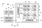
図1は、本発明の第1実施形態に係る立体視表示装置100のブロック図である。立体視表示装置100は、観察者に立体感を知覚させる立体視画像をアクティブシャッター方式で表示する電子機器であり、電気光学装置10と立体視用眼鏡20とを具備する。電気光学装置10は、右眼用画像GRと左眼用画像GLとを時分割で交互に表示する。
<A: First Embodiment>
FIG. 1 is a block diagram of a
立体視用眼鏡20は、電気光学装置10が表示する立体視画像の視認時に観察者が装着する眼鏡型の器具であり、観察者の右眼の前方に位置する右眼用シャッター22と左眼の前方に位置する左眼用シャッター24とを具備する。右眼用シャッター22および左眼用シャッター24の各々は、照射光を透過させる開状態(透過状態)と照射光を遮断する閉状態(遮光状態)とに制御される。例えば印加電圧に応じて液晶の配向方向を変化させることで開状態および閉状態の一方から他方に変化する液晶シャッターが右眼用シャッター22および左眼用シャッター24として採用され得る。
The
図1の電気光学装置10は、電気光学パネル12と制御回路14とを具備する。電気光学パネル12は、複数の画素回路(画素)PIXが配列された画素部30と、各画素回路PIXを駆動する駆動回路40とを含む。画素部30には、x方向に延在するM本の走査線32と、x方向に交差するy方向に延在するN本の信号線34とが形成される(MおよびNは自然数)。画素部30内の複数の画素回路PIXは、走査線32と信号線34との各交差に対応して縦M行×横N列の行列状に配列される。すなわち、x方向に配列するN個の画素回路PIXの集合(以下「画素回路群」という)BのM行分がy方向に並列に設置される。
The electro-
駆動回路40は、走査線駆動回路42と信号線駆動回路44とを具備する。走査線駆動回路42は、各走査線32に対応する走査信号Y[1]〜Y[M]の供給で各走査線32(各画素回路群B)を順次に選択する。走査信号Y[m](m=1〜M)が選択電位に設定されることで第m行の走査線32が選択される。信号線駆動回路44は、走査線駆動回路42による走査線32の選択に同期してN本の信号線34の各々に階調信号X[1]〜X[N]を供給する。階調信号X[n](n=1〜N)は、外部回路から供給される画像信号での指定階調(表示画像の各画素値)に応じて電位VGが可変に設定される電圧信号であり、所定の基準電位に対する極性が周期的に反転する。
The
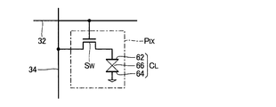
図2は、各画素回路PIXの回路図である。図2に示すように、各画素回路PIXは、液晶素子CLと選択スイッチSWとを含む。液晶素子CLは、相対向する画素電極62および共通電極64と両電極間の液晶66とで構成された電気光学素子である。画素電極62と共通電極64との間の印加電圧に応じて液晶66の透過率(表示階調)が変化する。選択スイッチSWは、走査線32にゲートが接続されたNチャネル型の薄膜トランジスターで構成され、液晶素子CLと信号線34との間に介在して両者の電気的な接続(導通/絶縁)を制御する。走査信号Y[m]が選択電位に設定されることで第m行の各画素回路PIXにおける選択スイッチSWが同時にオン状態に遷移する。各画素回路PIX(液晶素子CL)は、選択スイッチSWがオン状態に制御されたとき(すなわち走査線32の選択時)の階調信号X[n]の電位VGに応じた階調を表示する。なお、液晶素子CLに並列に補助容量を接続した構成も採用され得る。
FIG. 2 is a circuit diagram of each pixel circuit PIX. As shown in FIG. 2, each pixel circuit PIX includes a liquid crystal element CL and a selection switch SW. The liquid crystal element CL is an electro-optical element composed of the
図1の制御回路14は、電気光学パネル12を制御する表示制御回路142と、立体視用眼鏡20を制御する眼鏡制御回路144を具備する。なお、表示制御回路142と眼鏡制御回路144とを単体の集積回路に搭載した構成や、表示制御回路142と眼鏡制御回路144とを別体の集積回路に分散した構成が採用され得る。表示制御回路142は、相互に視差が付与された右眼用画像GRと左眼用画像GLとが時分割で画素部30に表示されるように駆動回路40を制御する。具体的には、表示制御回路142は、駆動回路40が以下の動作を実行するように駆動回路40を制御する。
The
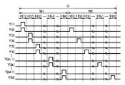
図3は、電気光学装置10の動作の説明図である。電気光学装置10の動作期間は、右眼用画像GRを表示するための右眼用期間PRと左眼用画像GLを表示するための左眼用期間PLとに区分される。各右眼用期間PRと各左眼用期間PLとは時間軸上に交互に配置される。右眼用期間PRおよび左眼用期間PLの各々は複数(偶数個)の単位期間Uを含む。第1実施形態では右眼用期間PRと左眼用期間PLの各々が2個の単位期間U(U1,U2)を含む場合を想定する。各単位期間Uは、第1書込期間W1と第2書込期間W2とに区分される。第2書込期間W2は第1書込期間W1に後続する。図3に示すように、第1書込期間W1および第2書込期間W2の各々は、表示制御回路142から走査線駆動回路42および信号線駆動回路44に供給される垂直同期信号VSYNCの1周期として規定される。
FIG. 3 is an explanatory diagram of the operation of the electro-
図4は、右眼用期間PRおよび左眼用期間PLの各々における各単位期間U(U1,U2)での走査線駆動回路42の動作の説明図である。図4に示すように、走査線駆動回路42は、各単位期間Uの第1書込期間W1において、相互に隣合う2本の走査線32(画素回路群Bの2行分)を選択単位として選択期間H[1]〜H[K]にて順次に選択する。すなわち、各第1書込期間W1の第k番目(k=1〜K)の選択期間H[k]では、奇数行の走査信号Y[2k-1]と偶数行の走査信号Y[2k]とが同時に選択電位に設定されることで、第(2k-1)行の走査線32(奇数行の画素回路群B)と第2k行の走査線32(偶数行の画素回路群B)とが同時に選択される。例えば選択期間H[1]では第1行の走査線32と第2行の走査線32とが同時に選択され、選択期間H[2]では第3行の走査線32と第4行の走査線32とが同時に選択される。したがって、第1書込期間W1内の選択期間H[k]の総数Kは、走査線32の総数(画素回路群Bの行数)Mの半分に相当する(K=M/2)。各選択期間H[k]で同時に選択される選択単位(2本の走査線32)のうち1本の走査線32(第1実施形態では第(2k-1)行の走査線32)を以下では「特定走査線32」と表記する。
FIG. 4 is an explanatory diagram of the operation of the scanning
他方、右眼用期間PRおよび左眼用期間PLの各々における各単位期間Uの第2書込期間W2において、走査線駆動回路42は、直前の第1書込期間W1で選択した各選択単位のうち特定走査線32以外の複数(M/2本)の走査線32を選択期間H[1]〜H[K]にて1本ずつ順次に選択する。すなわち、第2書込期間W2内の第k番目の選択期間H[k]では、走査信号Y[2k]が選択電位に設定されることで第2k行の1本の走査線32(第2k行の画素回路群B)が選択される。例えば選択期間H[1]では第2行の走査線32が選択され、選択期間H[2]では第4行の走査線32が選択される。したがって、各第2書込期間W2には第1書込期間W1と同様にK個(M/2個)の選択期間H[1]〜H[K]が含まれる。
On the other hand, in the second writing period W2 of each unit period U in each of the right eye period PR and the left eye period PL, the scanning
図3に示すように、信号線駆動回路44は、右眼用画像GRの各画素の指定階調(画素値)に応じた電位VGの階調信号X[1]〜X[N]を右眼用期間PR内の選択期間H[k]毎に各信号線34に供給し、左眼用画像GLの各画素の指定階調に応じた電位VGの階調信号X[1]〜X[N]を左眼用期間PL内の選択期間H[k]毎に各信号線34に供給する。図3に示すように、右眼用期間PRおよび左眼用期間PLの各々において、各画素回路PIXの液晶素子CLの印加電圧が前後の単位期間Uで逆極性となるように、各階調信号X[n]の電位VGの極性が単位期間U毎に順次に反転される。具体的には、階調信号X[n]の電位VGは、右眼用期間PRおよび左眼用期間PLの各々の単位期間U1では基準電位(例えば共通電極64の電位)に対して正極性(+)に設定され、単位期間U2では基準電位に対して負極性(-)に設定される。
As shown in FIG. 3, the signal
右眼用期間PRの各単位期間U(U1,U2)の第1書込期間W1のうち第(2k-1)行の走査線32と第2k行の走査線32とが同時に選択される選択期間H[k]において、信号線駆動回路44は、右眼用画像GRのうち特定走査線32(すなわち第(2k-1)行の走査線32)に対応する各画素の指定階調に応じた電位VGの階調信号X[n]を各信号線34に供給する。すなわち、図3に符号(A)で示すように、第1書込期間W1の選択期間H[k]では、第(2k-1)行および第2k行の各画素回路PIXに対して、右眼用画像GRのうち第(2k-1)行の各画素の指定階調GR[2k-1]に応じた電位VGが供給される。例えば、選択期間H[1]では、右眼用画像GRのうち第1行の各画素の指定階調GR[1]に応じた電位VGが第1行および第2行の各画素回路PIXに供給され、選択期間H[2]では、右眼用画像GRのうち第3行の各画素の指定階調GR[3]に応じた電位VGが第3行および第4行の各画素回路PIXに供給される。以上の通り、Y方向に相互に隣合う各画素回路PIXには相等しい電位VGが供給されるから、第1書込期間W1が終了する時点では、Y方向の解像度を半分に低下させた右眼用画像GRが画素部30に表示される。
Selection in which the (2k-1)
左眼用期間PLの各単位期間Uの第1書込期間W1でも同様に、図3に符号(C)で示すように、左眼用画像GLのうち第(2k-1)行の各画素の指定階調GL[2k-1]に応じた電位VGの階調信号X[n]が、第(2k-1)行および第2k行の各画素回路PIXに供給される。すなわち、例えば選択期間H[1]では、左眼用画像GLのうち第1行の各画素の指定階調GL[1]に応じた電位VGが第1行および第2行の各画素回路PIXに供給され、選択期間H[2]では、左眼用画像GLのうち第3行の各画素の指定階調GL[3]に応じた電位VGが第3行および第4行の各画素回路PIXに供給される。以上に説明した通り、右眼用期間PRおよび左眼用期間PLの各々の第1書込期間W1では、各画素回路PIXに対する電位VGの供給(書込)が選択期間H[k]毎に画素回路群Bの2行ずつ(すなわち選択単位毎に)順次に実行される。 Similarly, in the first writing period W1 of each unit period U of the left-eye period PL, each pixel in the (2k-1) th row of the left-eye image GL as indicated by reference numeral (C) in FIG. The gradation signal X [n] having the potential VG corresponding to the designated gradation GL [2k-1] is supplied to the pixel circuits PIX in the (2k-1) th and 2kth rows. That is, for example, in the selection period H [1], the potential VG corresponding to the designated gradation GL [1] of each pixel in the first row in the left eye image GL is set to each pixel circuit PIX in the first row and second row. In the selection period H [2], the potential VG corresponding to the designated gradation GL [3] of each pixel in the third row in the left-eye image GL is supplied to each pixel circuit in the third row and the fourth row. Supplied to PIX. As described above, in the first writing period W1 of each of the right eye period PR and the left eye period PL, the supply (writing) of the potential VG to each pixel circuit PIX is performed every selection period H [k]. It is sequentially executed for every two rows of the pixel circuit group B (that is, for each selection unit).
他方、右眼用期間PRの各単位期間U(U1,U2)の第2書込期間W2のうち第2k行の走査線32が選択される選択期間H[k]において、信号線駆動回路44は、図3に符号(B)で示すように、右眼用画像GRのうち当該走査線32(すなわち選択単位のうち特定走査線32以外の走査線32)に対応する第2k行の各画素の指定階調GR[2k]に応じた電位VGの階調信号X[n]を各信号線34に供給する。具体的には、選択期間[1]では、右眼用画像GRのうち第2行の各画素の指定階調GR[2]に応じた電位VGの階調信号X[n]が第2行の各画素回路PIXに供給され、選択期間H[2]では、右眼用画像GRのうち第4行の各画素の指定階調GR[4]に応じた電位VGの階調信号X[n]が第4行の各画素回路PIXに供給される。他方、奇数行(すなわち各選択単位での特定走査線32)に対応する各画素回路PIXの液晶素子CLの印加電圧は、直前の第1書込期間W1での印加電圧に保持される。したがって、第1書込期間W1の終点ではY方向に半分の解像度で表示されていた右眼用画像GRが、第2書込期間W2の終点では所期の解像度(M行×N列)の右眼用画像GRに更新される。
On the other hand, in the selection period H [k] in which the second k-
左眼用期間PLの各単位期間Uの第2書込期間W2でも同様に、図3に符号(D)で示すように、第2k行の走査線32が選択される選択期間H[k]において、左眼用画像GLのうち当該走査線32に対応する第2k行の各画素の指定階調GL[2k]に応じた電位VGの階調信号X[n]を各信号線34に供給する。例えば選択期間[1]では、左眼用画像GLのうち第2行の各画素の指定階調GL[2]に応じた電位VGの階調信号X[n]が第2行の各画素回路PIXに供給され、選択期間H[2]では、左眼用画像GLのうち第4行の各画素の指定階調GL[4]に応じた電位VGの階調信号X[n]が第4行の各画素回路PIXに供給される。以上に説明した通り、右眼用期間PRおよび左眼用期間PLの各々の第2書込期間W2では、第1書込期間W1での各選択単位のうち特定走査線32以外の走査線32に対応する各画素回路PIX(すなわち1行おきに選択された各画素回路PIX)について電位VGの供給(書込)が選択期間H[k]毎に順次に実行される。
Similarly, in the second writing period W2 of each unit period U of the left eye period PL, as indicated by a symbol (D) in FIG. 3, the selection period H [k] in which the 2k-
右眼用期間PR内の最初の第1書込期間W1では、直前の左眼用期間PL(単位期間U2内の第2書込期間W2)で表示された左眼用画像GLが各選択期間H[k]にて2行毎に右眼用画像GRに変更され、左眼用期間PL内の最初の第1書込期間W1では、直前の右眼用期間PRで表示された右眼用画像GRが各選択期間H[k]にて2行毎に左眼用画像GLに変更される。すなわち、右眼用期間PRおよび左眼用期間PLの各々の最初の第1書込期間W1では右眼用画像GRと左眼用画像GLとが混在する。 In the first first writing period W1 in the right eye period PR, the left eye image GL displayed in the immediately preceding left eye period PL (second writing period W2 in the unit period U2) is selected in each selection period. In H [k], the image is changed to the right-eye image GR every two lines, and in the first first writing period W1 in the left-eye period PL, the right-eye image displayed in the immediately previous right-eye period PR is displayed. The image GR is changed to the left eye image GL every two rows in each selection period H [k]. That is, the right eye image GR and the left eye image GL are mixed in the first first writing period W1 of each of the right eye period PR and the left eye period PL.
制御回路14の眼鏡制御回路144は、立体視用眼鏡20の右眼用シャッター22および左眼用シャッター24の各々の状態(開状態/閉状態)を電気光学パネル12の動作に同期して制御する。すなわち、眼鏡制御回路144は、図3に示すように、右眼用期間PRの最初の第1書込期間W1の始点から所定の時間が経過した時点で右眼用シャッター22を閉状態から開状態に変化させ、左眼用期間PLの始点にて右眼用シャッター22を開状態から閉状態に変化させたうえで左眼用期間PLの全体で閉状態に維持する。具体的には、右眼用期間PRの最初の第1書込期間W1の終点で右眼用シャッター22は閉状態から開状態に遷移する。同様に、眼鏡制御回路144は、左眼用期間PLの最初の第1書込期間W1の始点から所定の時間が経過した時点で左眼用シャッター24を閉状態から開状態に変化させ、右眼用期間PRの始点にて左眼用シャッター24を開状態から閉状態に変化させたうえで右眼用期間PRの全体で閉状態に維持する。具体的には、左眼用期間PLの最初の第1書込期間W1の終点で左眼用シャッター24は閉状態から開状態に遷移する。
The glasses control
したがって、右眼用期間PRのうち単位期間U1内の第2書込期間W2と直後の単位期間U2とで表示される右眼用画像GRは右眼用シャッター22を透過して観察者の右眼に到達するとともに左眼用シャッター24で遮断される。他方、左眼用期間PLのうち単位期間U1内の第2書込期間W2と直後の単位期間U2とで表示される左眼用画像GLは左眼用シャッター24を透過して観察者の左眼に到達するとともに右眼用シャッター22で遮断される。右眼用シャッター22を透過した右眼用画像GRを右眼で視認するとともに左眼用シャッター24を透過した左眼用画像GLを左眼で視認することで、観察者は表示画像に立体感を知覚する。
Accordingly, the right-eye image GR displayed in the second writing period W2 in the unit period U1 and the immediately subsequent unit period U2 in the right-eye period PR passes through the right-
図3に示すように、右眼用期間PRおよび左眼用期間PLの最初の第1書込期間W1では右眼用シャッター22および左眼用シャッター24の双方が閉状態に制御される。前述のように最初の第1書込期間W1では表示画像が右眼用画像GRおよび左眼用画像GLの一方から他方に2行毎に変化するが、右眼用シャッター22および左眼用シャッター24の双方が閉状態に維持されるから、右眼用画像GRと左眼用画像GLとの混在(クロストーク)は観察者に知覚されない。すなわち、右眼用画像GRと左眼用画像GLとが確実に右眼および左眼に分離されるから、観察者に明確な立体感を知覚させることが可能である。
As shown in FIG. 3, in the first first writing period W1 of the right eye period PR and the left eye period PL, both the
以上の形態においては、各第1書込期間W1では画素回路群Bを2行単位で選択して各画素回路PIXに階調信号X[n](電位VG)を供給する。したがって、右眼用期間PRおよび左眼用期間PLの最初に画素回路群Bを1行単位で順次に選択して階調信号X[n]を供給する構成と比較すると、右眼用画像GRと左眼用画像GLとが混在する期間(すなわち右眼用シャッター22および左眼用シャッター24の双方を閉状態に維持すべき期間)の時間長が短縮される。すなわち、右眼用シャッター22および左眼用シャッター24の一方を開状態に維持する時間長が充分に確保される。したがって、観察者が認識する表示画像の明るさを向上することが可能である。なお、第1書込期間W1では表示画像のY方向の解像度が低下するが、直後の第2書込期間W2では特定走査線32以外の走査線32に対応する各画素回路PIXに階調信号X[n]が供給されるから、表示画像の解像度の低下は観察者に殆ど認識されない。
In the above embodiment, the pixel circuit group B is selected in units of two rows in each first writing period W1, and the gradation signal X [n] (potential VG) is supplied to each pixel circuit PIX. Therefore, when compared with the configuration in which the pixel circuit group B is sequentially selected in units of one row and the gradation signal X [n] is supplied at the beginning of the right eye period PR and the left eye period PL, the right eye image GR is compared. And the left eye image GL are mixed (that is, the period during which both the
また、第1実施形態では、右眼用期間PRおよび左眼用期間PLの各々が複数の単位期間Uを含み、相前後する各単位期間Uで液晶素子CLの印加電圧の極性が反転される。すなわち、例えば右眼用期間PRと左眼用期間PLとで液晶素子CLの印加電圧の極性を反転させる場合と比較して液晶素子CLの印加電圧の極性反転の周期が短縮されるから、直流成分の印加に起因した液晶素子CLの特性劣化を有効に防止できるという利点がある。 In the first embodiment, each of the right-eye period PR and the left-eye period PL includes a plurality of unit periods U, and the polarity of the voltage applied to the liquid crystal element CL is inverted in each successive unit period U. . That is, for example, compared with the case where the polarity of the applied voltage of the liquid crystal element CL is reversed in the right eye period PR and the left eye period PL, the polarity reversal period of the applied voltage of the liquid crystal element CL is shortened. There is an advantage that the characteristic deterioration of the liquid crystal element CL due to the application of the components can be effectively prevented.
なお、右眼用画像GRと左眼用画像GLとでは各画素の指定階調が相違するから、右眼用期間PRと左眼用期間PLとで液晶素子CLの印加電圧の極性を反転させる構成では、例えば右眼用期間PRにて液晶素子CLに印加される正極性電圧と左眼用期間PLにて液晶素子CLに印加される負極性電圧との差異が顕著となり、液晶素子CLに対する直流成分の印加を抑制することが困難となる。他方、第1実施形態では、右眼用画像GRが表示される右眼用期間PR内の単位期間U毎に液晶素子CLの印加電圧の極性が反転され、かつ、左眼用画像GLが表示される左眼用期間PL内の単位期間U毎に液晶素子CLの印加電圧の極性が反転される。したがって、右眼用画像GRと左眼用画像GLとの相違に関わらず、液晶素子CLの印加電圧の極性の偏向(直流成分の残留)を有効に抑制できるという利点がある。以上の例示では特に、右眼用期間PRおよび左眼用期間PLの各々が偶数個の単位期間Uを含むから、右眼用期間PRおよび左眼用期間PLの各々において、各画素回路PIXの液晶素子CLに正極性電圧が印加される時間長と負極性電圧が印加される時間長とが均等化される。したがって、液晶素子CLの印加電圧の極性の偏向を抑制できるという効果は格別に顕著である。 Since the designated gradation of each pixel differs between the right eye image GR and the left eye image GL, the polarity of the voltage applied to the liquid crystal element CL is inverted between the right eye period PR and the left eye period PL. In the configuration, for example, the difference between the positive voltage applied to the liquid crystal element CL in the right eye period PR and the negative voltage applied to the liquid crystal element CL in the left eye period PL becomes significant, and the difference between the positive voltage and the liquid crystal element CL is significant. It becomes difficult to suppress application of a direct current component. On the other hand, in the first embodiment, the polarity of the voltage applied to the liquid crystal element CL is inverted every unit period U in the right eye period PR in which the right eye image GR is displayed, and the left eye image GL is displayed. The polarity of the voltage applied to the liquid crystal element CL is inverted every unit period U within the left eye period PL. Therefore, regardless of the difference between the image for the right eye GR and the image for the left eye GL, there is an advantage that the polarity of the applied voltage of the liquid crystal element CL (residual DC component) can be effectively suppressed. In the above example, in particular, since each of the right eye period PR and the left eye period PL includes an even number of unit periods U, each of the pixel circuits PIX in each of the right eye period PR and the left eye period PL. The time length in which the positive voltage is applied to the liquid crystal element CL and the time length in which the negative voltage is applied are equalized. Therefore, the effect of suppressing the polarity deviation of the applied voltage of the liquid crystal element CL is particularly remarkable.
<B:第2実施形態>
本発明の第2実施形態を以下に説明する。なお、以下に例示する各形態において作用や機能が第1実施形態と同等である要素については、以上の説明で参照した符号を流用して各々の詳細な説明を適宜に省略する。
<B: Second Embodiment>
A second embodiment of the present invention will be described below. In addition, about the element which an effect | action and a function are equivalent to 1st Embodiment in each form illustrated below, each reference detailed in the above description is diverted and each detailed description is abbreviate | omitted suitably.
図5は、第2実施形態における走査線駆動回路42の動作の説明図である。第1実施形態では、第1書込期間W1の各選択期間H[k]で同時に選択する複数の走査線32(選択単位)の組合せを単位期間U1と単位期間U2とで共通させた。第2実施形態では、第1書込期間W1にて選択単位として選択する走査線32の組合せを単位期間U1と単位期間U2とで相違させる。
FIG. 5 is an explanatory diagram of the operation of the scanning
具体的には、右眼用期間PRおよび左眼用期間PLの各々における単位期間U1の第1書込期間W1では、走査線駆動回路42は、第1実施形態と同様に、第(2k-1)行の走査線32と第2k行の走査線32との組合せを選択単位として選択期間H[k]毎に順次に選択する。すなわち、図6に符号(A)で示すように、例えば選択期間H[1]では第1行の走査線32と第2行の走査線32とが同時に選択され、選択期間H[2]では第3行の走査線32と第4行の走査線32とが同時に選択される。そして、第1書込期間W1内の各選択期間H[k]では、右眼用画像GRまたは左眼用画像GLのうち第(2k-1)行の走査線32(特定走査線32)に対応する各画素の指定階調(GR[2k-1],GL[2k-1])に応じた電位VGが選択単位の各画素回路PIXに供給される。また、図6に符号(B)で示すように、直後の第2書込期間W2では選択単位のうち特定走査線32以外の走査線32に対応する各画素回路PIXに電位VGの階調信号X[n]が供給される。
Specifically, in the first writing period W1 of the unit period U1 in each of the right eye period PR and the left eye period PL, the scanning
他方、右眼用期間PRおよび左眼用期間PLの各々における単位期間U2の第1書込期間W1では、図6に符号(C)で示すように、走査線駆動回路42は、第2k行の走査線32と第(2k+1)行の走査線32との組合せを選択単位として選択期間H[k]毎に順次に選択する。具体的には、図5に示すように、第1書込期間W1内の第k番目の選択期間H[k]では、偶数行の走査信号Y[2k]と奇数行の走査信号Y[2k+1]とが同時に選択電位に設定される。すなわち、例えば選択期間H[1]では第2行の走査線32と第3行の走査線32とが同時に選択され、選択期間H[2]では第4行の走査線32と第5行の走査線32とが同時に選択される。単位期間U2内の第1書込期間W1の各選択期間H[k]では第2k行の走査線32が特定走査線32として選定される。すなわち、各選択期間H[k]では、右眼用画像GRまたは左眼用画像GLのうち第2k行の走査線32(特定走査線32)に対応する各画素の指定階調(GR[2k],GL[2k])に応じた電位VGが選択単位(2行分)の各画素回路PIXに供給される。
On the other hand, in the first writing period W1 of the unit period U2 in each of the right-eye period PR and the left-eye period PL, the scanning
以上の説明から理解されるように、第1書込期間W1にて各選択単位を構成する2本の走査線32の組合せ(すなわち電位VGの供給対象となる画素回路群Bの組合せ)は単位期間U1と単位期間U2とで1行分だけずれた関係となる。ただし、各画素回路PIXに対する電位VGの供給(書込)が画素回路群Bの2行ずつ選択期間H[k]毎に順次に実行されるという動作は単位期間U1と単位期間U2とで同様である。
As can be understood from the above description, the combination of the two
単位期間U2内の第2書込期間W2では、各選択単位のうち特定走査線32以外の走査線32に対応する各画素回路PIXに電位VGが供給される。すなわち、図6に符号(D)で示すように、第(2k-1)行(第1行,第3行,第5行,……)の各走査線32が順次に選択されるとともに右眼用画像GRおよび左眼用画像GLのうち当該走査線32に対応する各画素の指定階調(GR[2k-1],GL[2k-1])に応じた電位VGの階調信号X[n]が各信号線34に供給される。すなわち、第2書込期間W2にて選択される走査線32(電位VGの供給対象となる画素回路群B)は単位期間U1と単位期間U2とで相違する。
In the second writing period W2 in the unit period U2, the potential VG is supplied to each pixel circuit PIX corresponding to the
第2実施形態においても第1実施形態と同様の効果が実現される。ところで、M本の走査線32のうち特定走査線32に対応する各画素回路PIXについては各単位期間U内で1回だけ電位VGの供給が実行され、特定走査線32以外の走査線32に対応する各画素回路PIXには単位期間U内で2回の電位VGの供給が実行されるという相違がある。そして、特定走査線32の各画素回路PIXとそれ以外の走査線32の各画素回路PIXとでは、各々に供給される電位VGが仮に相等しい場合(すなわち同等の階調が指定された場合)でも、電位VGの供給回数(あるいは供給間隔)の差異に起因して表示階調に相違が発生し得る。第1実施形態では、奇数行の各走査線32が固定的に特定走査線32とされるから、画素部30内の全部の画素回路PIXに同等の電位VGを供給した場合でも、各画素回路PIXの表示階調が奇数行と偶数行とで相違する(すなわち行単位の表示斑が発生する)可能性がある。他方、第2実施形態では、単位期間U1にて奇数行の各走査線32が特定走査線32とされ、単位期間U2内では偶数行の各走査線32が特定走査線32とされる。したがって、奇数行の各画素回路PIXの表示階調と偶数行の各画素回路PIXの表示階調との相違(表示斑)が観察者に知覚され難くなるという利点がある。
In the second embodiment, the same effect as in the first embodiment is realized. By the way, for each pixel circuit PIX corresponding to the
<C:変形例>
以上の各形態は多様に変形され得る。具体的な変形の態様を以下に例示する。以下の例示から任意に選択された2以上の態様は、相互に矛盾しない範囲内で適宜に併合され得る。
<C: Modification>
Each of the above forms can be variously modified. Specific modifications are exemplified below. Two or more aspects arbitrarily selected from the following examples can be appropriately combined within a range that does not contradict each other.
(1)変形例1
第1書込期間W1にて同時に選択する走査線32の本数(選択単位を構成する走査線32の本数)は、以上に例示した2本に限定されない。選択単位を構成する走査線32の本数をH本と一般化した場合、各単位期間UがH個の書込期間W1〜WHに区分される。そして、各単位期間Uのうち最初の書込期間W1では選択単位(H本の走査線32)がK個(K=M/H)の選択期間H[1]〜H[K]の各々で順次に同時に選択され、かつ、右眼用画像GRまたは左眼用画像GLのうち特定走査線32に対応する各画素の指定階調に応じた電位VGが選択単位内の各画素回路PIXに供給される。また、単位期間U内の第2番目以降の各書込期間Wh(h=2〜H)では、選択単位内の第h番目の1本の走査線32が選択され、かつ、右眼用画像GRまたは左眼用画像GLのうち当該走査線32に対応する各画素の指定階調に応じた電位VGが供給される。選択単位を構成する走査線32の組合せを単位期間U毎に相違させる第2実施形態の構成も同様に採用される。
(1)
The number of
(2)変形例2
以上の各形態では、右眼用期間PRのうち最初の第1書込期間W1の終点にて右眼用シャッター22を閉状態から開状態に変化させたが、右眼用シャッター22を開状態に変化させる時期は適宜に変更される。例えば、右眼用期間PRの最初の第1書込期間W1の終点以前に右眼用シャッター22を開状態に変更する構成では、第1書込期間W1内での右眼用画像GRと左眼用画像GLとの混在が観察者に若干は知覚されるが、表示画像の明度を向上させることが可能である。他方、右眼用期間PRの最初の第1書込期間W1の終点以降の時点で右眼用シャッター22を開状態に変更する構成では、右眼用画像GRと左眼用画像GLとの混在が観察者に知覚されることを確実に防止することが可能である。すなわち、右眼用シャッター22を開状態に変化させる時期は、右眼用期間PRのうち最初の第1書込期間W1の始点から所定の時間(すなわち右眼用画像GRと左眼用画像GLとの混在が利用者に知覚されることを防止する必要がある期間)が経過した時点として包括され、右眼用画像GRと左眼用画像GLとの混在を利用者に知覚されることの防止と表示画像の明度の確保との優先度(バランス)に応じて適宜に選定される。左眼用期間PL内で左眼用シャッター24を閉状態から開状態に変化させる時期も同様であり、左眼用期間PLのうち最初の第1書込期間W1の始点から所定の時間が経過した任意の時点が、右眼用画像GRと左眼用画像GLとの混在が利用者に知覚されることの防止と表示画像の明度の確保との優先度に応じて適宜に選定される。また、右眼用画像GRと左眼用画像GLとの混在が利用者に知覚され難い開閉の時期は、右眼用シャッター22および左眼用シャッター24の応答特性と電気光学パネル12(液晶素子CL)の応答特性との関係に応じて変化する。したがって、右眼用シャッター22および左眼用シャッター24の各々を開状態および閉状態の一方から他方に変化させる時期を、立体視用眼鏡20の応答特性と電気光学パネル12の応答特性との関係に応じて選定した構成も好適である。
(2)
In each of the above embodiments, the right-
同様に、右眼用シャッター22を開状態から閉状態に変化させる時期は、右眼用期間PRの終点(左眼用期間PLの始点)に限定されない。例えば、右眼用期間PRの終点を含む所定の期間内(終点の到来前または経過後)に右眼用シャッター22を閉状態に変化させることも可能である。また、左眼用シャッター24を開状態から閉状態に変化させる時期も任意であり、例えば、左眼用期間PLの終点(右眼用期間PRの始点)を含む所定の期間内に左眼用シャッター24を閉状態に変化させる構成も採用され得る。
Similarly, the time when the right-
(3)変形例3
液晶素子CLの印加電圧の極性を反転させる周期は本発明において任意である。例えば、右眼用期間PRと左眼用期間PLとで印加電圧の極性を反転させる構成や、右眼用期間PRと左眼用期間PLとの対を1周期として印加電圧の極性を反転させる構成が採用され得る。
(3)
The period for reversing the polarity of the voltage applied to the liquid crystal element CL is arbitrary in the present invention. For example, the polarity of the applied voltage is reversed between the right eye period PR and the left eye period PL, or the polarity of the applied voltage is reversed with one pair of the right eye period PR and the left eye period PL as one cycle. A configuration may be employed.
(4)変形例4
右眼用期間PRおよび左眼用期間PLの各々に含まれる単位期間Uの個数は任意である。例えば右眼用期間PRおよび左眼用期間PLの各々が3個以上の単位期間Uを含む構成も採用され得る。もっとも、液晶素子CLの印加電圧の極性を単位期間U毎に反転させる構成のもとで液晶素子CLに対する直流成分の印加を有効に防止するという観点からすると、前述のように右眼用期間PRおよび左眼用期間PLの各々が偶数個の単位期間Uを含む構成が格別に好適である。
(4)
The number of unit periods U included in each of the right eye period PR and the left eye period PL is arbitrary. For example, a configuration in which each of the right eye period PR and the left eye period PL includes three or more unit periods U may be employed. However, from the viewpoint of effectively preventing application of a direct current component to the liquid crystal element CL under the configuration in which the polarity of the applied voltage of the liquid crystal element CL is reversed every unit period U, as described above, the right eye period PR A configuration in which each of the left eye periods PL includes an even number of unit periods U is particularly suitable.
(5)変形例5
電気光学素子は液晶素子CLに限定されない。例えば、電気泳動素子を電気光学素子として利用することも可能である。すなわち、電位光学素子は、電気的な作用(例えば電圧の印加)に応じて光学的な特性(例えば透過率)が変化する表示素子として包括される。
(5)
The electro-optical element is not limited to the liquid crystal element CL. For example, an electrophoretic element can be used as an electro-optical element. That is, the potential optical element is included as a display element whose optical characteristics (for example, transmittance) change according to an electrical action (for example, application of voltage).
<D:応用例>
以上の各形態に例示した電気光学装置10は、各種の電子機器に利用され得る。図7から図9には、電気光学装置10を採用した電子機器の具体的な形態が例示されている。
<D: Application example>
The electro-
図7は、電気光学装置10を採用した可搬型のパーソナルコンピューターの斜視図である。パーソナルコンピューター2000は、各種の画像を表示する電気光学装置10と、電源スイッチ2001やキーボード2002が設置された本体部2010とを具備する。
FIG. 7 is a perspective view of a portable personal computer employing the electro-
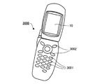
図8は、電気光学装置10を適用した携帯電話機の斜視図である。携帯電話機3000は、複数の操作ボタン3001およびスクロールボタン3002と、各種の画像を表示する電気光学装置10とを備える。スクロールボタン3002を操作することによって、電気光学装置10に表示される画面がスクロールされる。
FIG. 8 is a perspective view of a mobile phone to which the electro-
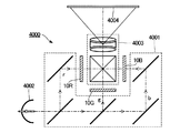
図9は、電気光学装置10を適用した投射型表示装置(3板式のプロジェクター)4000の模式図である。投射型表示装置4000は、相異なる表示色(赤色,緑色,青色)に対応する3個の電気光学装置10(10R,10G,10B)を含んで構成される。照明光学系4001は、照明装置(光源)4002からの出射光のうち赤色成分rを電気光学装置10Rに供給し、緑色成分gを電気光学装置10Gに供給し、青色成分bを電気光学装置10Bに供給する。各電気光学装置10は、照明光学系4001から供給される各単色光を表示画像に応じて変調する光変調器(ライトバルブ)として機能する。投射光学系4003は、各電気光学装置10からの出射光を合成して投射面4004に投射する。観察者は、投射面4004に投射された立体視画像を立体視用眼鏡20で視認する。
FIG. 9 is a schematic diagram of a projection display device (three-plate projector) 4000 to which the electro-
なお、本発明に係る電気光学装置が適用される電子機器としては、図7から図9に例示した機器のほか、携帯情報端末(PDA:Personal Digital Assistants),デジタルスチルカメラ,テレビ,ビデオカメラ,カーナビゲーション装置,車載用の表示器(インパネ),電子手帳,電子ペーパー,電卓,ワードプロセッサ,ワークステーション,テレビ電話,POS端末,プリンター,スキャナー,複写機,ビデオプレーヤー,タッチパネルを備えた機器等などが挙げられる。 Note that electronic devices to which the electro-optical device according to the present invention is applied include, in addition to the devices illustrated in FIGS. 7 to 9, personal digital assistants (PDAs), digital still cameras, televisions, video cameras, Car navigation devices, in-vehicle displays (instrument panels), electronic notebooks, electronic paper, calculators, word processors, workstations, videophones, POS terminals, printers, scanners, copiers, video players, devices with touch panels, etc. Can be mentioned.
100……立体視表示装置、10……電気光学装置、12……電気光学パネル、14……制御回路、142……表示制御回路、144……眼鏡制御回路、20……立体視用眼鏡、22……右眼用シャッター、24……左眼用シャッター、30……画素部、PIX……画素回路、CL……液晶素子、SW……選択スイッチ、32……走査線、34……信号線、40……駆動回路、42……走査線駆動回路、44……信号線駆動回路。
DESCRIPTION OF
Claims (6)
相互に交差する走査線および信号線と、
前記走査線と前記信号線との交差に対応して配置された画素と、
交互に設けられる右眼用期間および左眼用期間の各々に含まれる第1書込期間において複数の前記走査線を選択単位として順次に選択し、前記右眼用画像または前記左眼用画像のうち前記複数の走査線における特定走査線に対応する画素の画像信号を前記信号線に供給し、前記第1書込期間の経過後の第2書込期間において、前記複数の走査線のうち前記特定走査線以外の走査線を順次に選択し、前記右眼用画像または前記左眼用画像のうち前記特定走査線以外の走査線に対応する画素の画像信号を前記信号線に供給する駆動回路と、
前記右眼用シャッターおよび前記左眼用シャッターの各々の開閉を制御する眼鏡制御回路とを具備し、
前記右眼用期間および前記左眼用期間は、複数の単位期間を含み、前記複数の単位期間の各々が、前記第1書込期間と前記第2書込期間とを含み、
前記駆動回路は、前記右眼用期間および前記左眼用期間の各々において、相前後する各単位期間で前記画素の印加電圧が逆極性となるように、前記信号線に画像信号を供給し、
前記眼鏡制御回路は、前記右眼用期間の最初の単位期間における前記第1書込期間の終点から当該右眼用期間の終点まで、当該右眼用期間の4分の3以上の時間長にわたり前記右眼用シャッターを開状態に制御することで前記右眼用画像を観察者の右眼により視認可能な状態を継続する一方、前記左眼用期間の最初の単位期間における前記第1書込期間の終点から当該左眼用期間の終点まで、当該左眼用期間の4分の3以上の時間長にわたり前記左眼用シャッターを開状態に制御することで前記左眼用画像を観察者の左眼により視認可能な状態を継続する
ことを特徴とする電気光学装置。 An electro-optical device that displays a right-eye image and a left-eye image stereoscopically viewed with stereoscopic glasses including a right-eye shutter and a left-eye shutter,
Scanning and signal lines intersecting each other;
A pixel disposed corresponding to an intersection of the scanning line and the signal line;
In the first writing period included in each of the right-eye period and the left-eye period that are alternately provided, a plurality of the scanning lines are sequentially selected as a selection unit, and the right-eye image or the left-eye image is selected. Among them, an image signal of a pixel corresponding to a specific scanning line in the plurality of scanning lines is supplied to the signal line, and the second writing period after the first writing period has passed, the out of the plurality of scanning lines A driving circuit that sequentially selects scanning lines other than the specific scanning line and supplies image signals of pixels corresponding to scanning lines other than the specific scanning line in the right-eye image or the left-eye image to the signal line. When,
A glasses control circuit for controlling opening and closing of each of the right eye shutter and the left eye shutter;
The right-eye period and the left-eye period include a plurality of unit periods, and each of the plurality of unit periods includes the first writing period and the second writing period,
The drive circuit supplies an image signal to the signal line so that an applied voltage of the pixel has a reverse polarity in each unit period in succession in each of the right-eye period and the left-eye period,
The glasses control circuit, from the end point of the first writing period in the first unit period of the right-eye period to the end of the right-eye period, over three or more time length of a quarter of the right-eye period The first writing in the first unit period of the left-eye period is continued while the right-eye shutter is kept open so that the right-eye image can be visually recognized by the observer's right eye. By controlling the left-eye shutter in an open state from the end point of the period to the end point of the left-eye period over a time length of three quarters or more of the left-eye period, the left-eye image is An electro-optical device characterized in that it remains visible with the left eye .
ことを特徴とする請求項1に記載の電気光学装置。 The electro-optical device according to claim 1 , wherein each of the right-eye period and the left-eye period includes an even number of the unit periods.
ことを特徴とする請求項1または請求項2の電気光学装置。 The drive circuit changes, for each first writing period, a combination of the plurality of scanning lines selected as the selection unit in the first writing period of each of the right eye period and the left eye period. The electro-optical device according to claim 1 , wherein the electro-optical device is provided.
ことを特徴とする請求項3の電気光学装置。 The drive circuit includes a combination of the plurality of scanning lines selected as the selection unit in one first writing period and another first writing in each of the right-eye period and the left-eye period. The plurality of scans selected as the selection unit in each first writing period so that the combination of the plurality of scanning lines selected as the selection unit in the period is shifted by one row of the scanning lines 4. The electro-optical device according to claim 3 , wherein a combination of lines is selected.
ことを特徴とする請求項1から請求項4の何れかの電気光学装置。 The electro-optical device according to any one of claims 1 to 4 , wherein the driving circuit sequentially selects a combination of two scanning lines adjacent to each other as the selection unit.
Priority Applications (3)
| Application Number | Priority Date | Filing Date | Title |
|---|---|---|---|
| JP2011003057A JP5771994B2 (en) | 2011-01-11 | 2011-01-11 | Electro-optical device and electronic apparatus |
| US13/344,389 US9030507B2 (en) | 2011-01-11 | 2012-01-05 | Electro-optical device and electronic apparatus |
| CN201210007415.2A CN102595161B (en) | 2011-01-11 | 2012-01-11 | Electro-optical device and electronic apparatus |
Applications Claiming Priority (1)
| Application Number | Priority Date | Filing Date | Title |
|---|---|---|---|
| JP2011003057A JP5771994B2 (en) | 2011-01-11 | 2011-01-11 | Electro-optical device and electronic apparatus |
Related Child Applications (1)
| Application Number | Title | Priority Date | Filing Date |
|---|---|---|---|
| JP2015132990A Division JP6102990B2 (en) | 2015-07-01 | 2015-07-01 | Electro-optical device and electronic apparatus |
Publications (3)
| Publication Number | Publication Date |
|---|---|
| JP2012145695A JP2012145695A (en) | 2012-08-02 |
| JP2012145695A5 JP2012145695A5 (en) | 2014-02-27 |
| JP5771994B2 true JP5771994B2 (en) | 2015-09-02 |
Family
ID=46454909
Family Applications (1)
| Application Number | Title | Priority Date | Filing Date |
|---|---|---|---|
| JP2011003057A Expired - Fee Related JP5771994B2 (en) | 2011-01-11 | 2011-01-11 | Electro-optical device and electronic apparatus |
Country Status (3)
| Country | Link |
|---|---|
| US (1) | US9030507B2 (en) |
| JP (1) | JP5771994B2 (en) |
| CN (1) | CN102595161B (en) |
Families Citing this family (3)
| Publication number | Priority date | Publication date | Assignee | Title |
|---|---|---|---|---|
| JP2014063013A (en) * | 2012-09-21 | 2014-04-10 | Seiko Epson Corp | Electro-optical device, its driving method and electronic apparatus |
| JP2014122951A (en) * | 2012-12-20 | 2014-07-03 | Seiko Epson Corp | Driving method of electro-optic device, driving device, electro-optic device, and electronic equipment |
| JP6255836B2 (en) * | 2013-09-20 | 2018-01-10 | セイコーエプソン株式会社 | DRIVE DEVICE, DRIVE METHOD, DISPLAY DEVICE, AND ELECTRONIC DEVICE |
Family Cites Families (8)
| Publication number | Priority date | Publication date | Assignee | Title |
|---|---|---|---|---|
| JP2004093717A (en) * | 2002-08-30 | 2004-03-25 | Hitachi Ltd | Liquid crystal display |
| JP5309488B2 (en) * | 2007-07-18 | 2013-10-09 | セイコーエプソン株式会社 | Electro-optical device and electronic apparatus |
| JP2010107580A (en) * | 2008-10-28 | 2010-05-13 | Necディスプレイソリューションズ株式会社 | Driving method and electro-optic device |
| JP5619365B2 (en) * | 2009-03-13 | 2014-11-05 | ソニー株式会社 | Image display device, image display observation system, and image display method |
| JP5526597B2 (en) * | 2009-05-19 | 2014-06-18 | ソニー株式会社 | Display device and display method |
| JP5273478B2 (en) * | 2009-07-07 | 2013-08-28 | ソニー株式会社 | Video display device and video display system |
| JP5876635B2 (en) | 2009-07-22 | 2016-03-02 | セイコーエプソン株式会社 | Electro-optical device drive device, electro-optical device, and electronic apparatus |
| JP2010224547A (en) * | 2010-04-19 | 2010-10-07 | Nano Loa Inc | Liquid crystal display device |
-
2011
- 2011-01-11 JP JP2011003057A patent/JP5771994B2/en not_active Expired - Fee Related
-
2012
- 2012-01-05 US US13/344,389 patent/US9030507B2/en active Active
- 2012-01-11 CN CN201210007415.2A patent/CN102595161B/en not_active Expired - Fee Related
Also Published As
| Publication number | Publication date |
|---|---|
| JP2012145695A (en) | 2012-08-02 |
| US9030507B2 (en) | 2015-05-12 |
| US20120176375A1 (en) | 2012-07-12 |
| CN102595161A (en) | 2012-07-18 |
| CN102595161B (en) | 2015-07-22 |
Similar Documents
| Publication | Publication Date | Title |
|---|---|---|
| JP5664017B2 (en) | Electro-optical device and electronic apparatus | |
| JP2013114143A (en) | Electro-optic device and electronic apparatus | |
| JP5891621B2 (en) | Electro-optical device and electronic apparatus | |
| JP2014063013A (en) | Electro-optical device, its driving method and electronic apparatus | |
| JP5771994B2 (en) | Electro-optical device and electronic apparatus | |
| JP5799709B2 (en) | Electro-optical device and electronic apparatus | |
| JP2013064920A (en) | Electro-optical device and electronic apparatus | |
| JP5780054B2 (en) | Electro-optical device and electronic apparatus | |
| JP5782874B2 (en) | Electro-optical device and electronic apparatus | |
| JP5842632B2 (en) | Electro-optical device and electronic apparatus | |
| JP6102990B2 (en) | Electro-optical device and electronic apparatus | |
| JP2013117554A (en) | Electro-optic device and electronic apparatus | |
| JP2013073036A (en) | Electro-optical device and electronic apparatus | |
| JP2013064824A (en) | Electro-optic device and electronic apparatus | |
| JP5821415B2 (en) | Electro-optical device and electronic apparatus | |
| JP2013044992A (en) | Electro-optical device and electronic apparatus | |
| JP5703768B2 (en) | Electro-optical device and electronic apparatus | |
| JP2014092603A (en) | Driving method and driving device for electro-optical apparatuses, electro-optical apparatus, and electronic equipment |
Legal Events
| Date | Code | Title | Description |
|---|---|---|---|
| A521 | Request for written amendment filed |
Free format text: JAPANESE INTERMEDIATE CODE: A523 Effective date: 20140109 |
|
| A621 | Written request for application examination |
Free format text: JAPANESE INTERMEDIATE CODE: A621 Effective date: 20140109 |
|
| A977 | Report on retrieval |
Free format text: JAPANESE INTERMEDIATE CODE: A971007 Effective date: 20140917 |
|
| A131 | Notification of reasons for refusal |
Free format text: JAPANESE INTERMEDIATE CODE: A131 Effective date: 20141001 |
|
| A521 | Request for written amendment filed |
Free format text: JAPANESE INTERMEDIATE CODE: A523 Effective date: 20141127 |
|
| A131 | Notification of reasons for refusal |
Free format text: JAPANESE INTERMEDIATE CODE: A131 Effective date: 20150127 |
|
| A521 | Request for written amendment filed |
Free format text: JAPANESE INTERMEDIATE CODE: A523 Effective date: 20150324 |
|
| RD04 | Notification of resignation of power of attorney |
Free format text: JAPANESE INTERMEDIATE CODE: A7424 Effective date: 20150403 |
|
| TRDD | Decision of grant or rejection written | ||
| A01 | Written decision to grant a patent or to grant a registration (utility model) |
Free format text: JAPANESE INTERMEDIATE CODE: A01 Effective date: 20150602 |
|
| A61 | First payment of annual fees (during grant procedure) |
Free format text: JAPANESE INTERMEDIATE CODE: A61 Effective date: 20150615 |
|
| R150 | Certificate of patent or registration of utility model |
Ref document number: 5771994 Country of ref document: JP Free format text: JAPANESE INTERMEDIATE CODE: R150 |
|
| S531 | Written request for registration of change of domicile |
Free format text: JAPANESE INTERMEDIATE CODE: R313531 |
|
| R350 | Written notification of registration of transfer |
Free format text: JAPANESE INTERMEDIATE CODE: R350 |
|
| LAPS | Cancellation because of no payment of annual fees | ||
| S111 | Request for change of ownership or part of ownership |
Free format text: JAPANESE INTERMEDIATE CODE: R313113 |
|
| R350 | Written notification of registration of transfer |
Free format text: JAPANESE INTERMEDIATE CODE: R350 |