JP5750439B2 - Piezoelectric strain device - Google Patents
Piezoelectric strain device Download PDFInfo
- Publication number
- JP5750439B2 JP5750439B2 JP2012518527A JP2012518527A JP5750439B2 JP 5750439 B2 JP5750439 B2 JP 5750439B2 JP 2012518527 A JP2012518527 A JP 2012518527A JP 2012518527 A JP2012518527 A JP 2012518527A JP 5750439 B2 JP5750439 B2 JP 5750439B2
- Authority
- JP
- Japan
- Prior art keywords
- holes
- depressions
- extending
- power generation
- generation device
- Prior art date
- Legal status (The legal status is an assumption and is not a legal conclusion. Google has not performed a legal analysis and makes no representation as to the accuracy of the status listed.)
- Expired - Fee Related
Links
Images
Classifications
-
- H—ELECTRICITY
- H10—SEMICONDUCTOR DEVICES; ELECTRIC SOLID-STATE DEVICES NOT OTHERWISE PROVIDED FOR
- H10N—ELECTRIC SOLID-STATE DEVICES NOT OTHERWISE PROVIDED FOR
- H10N30/00—Piezoelectric or electrostrictive devices
- H10N30/30—Piezoelectric or electrostrictive devices with mechanical input and electrical output, e.g. functioning as generators or sensors
-
- H—ELECTRICITY
- H10—SEMICONDUCTOR DEVICES; ELECTRIC SOLID-STATE DEVICES NOT OTHERWISE PROVIDED FOR
- H10N—ELECTRIC SOLID-STATE DEVICES NOT OTHERWISE PROVIDED FOR
- H10N35/00—Magnetostrictive devices
- H10N35/101—Magnetostrictive devices with mechanical input and electrical output, e.g. generators, sensors
Landscapes
- General Electrical Machinery Utilizing Piezoelectricity, Electrostriction Or Magnetostriction (AREA)
Description
(関連出願の引用)
本願は、2009年7月2日に出願された米国仮特許出願第61/270,080号に基づくものであり、該米国仮特許出願の利益を主張するものである。
(Citation of related application)
This application is based on US Provisional Patent Application No. 61 / 270,080 filed on July 2, 2009, and claims the benefit of the US Provisional Patent Application.
(発明の背景)
本願発明は、電子デバイスに電力供給するためのスタンドアローンの発電デバイスとして適した圧電磁歪デバイス(piezo magnetostrictive device)、または、例えば回転数、速度または空気圧等のタイヤの様々な機能を監視するために利用され得るタイプの無線周波数識別デバイス(RFID)のコンポーネントとして適した圧電磁歪デバイスに関する。タイヤとともに用いるRFIDデバイスの使用を示す特許は、本発明者の特許文献1を含む。RFIDデバイスを含むその他のデバイスであって、タイヤに関する様々な機能を監視するためのタイヤ構造の表面またはタイヤ構造内に組み込まれ得るその他のデバイスは、特許文献2、特許文献3、特許文献4、特許文献5、特許文献6、特許文献7、特許文献8を含む。これらの特許に含まれる開示は、本明細書において参照により援用される。
(Background of the Invention)
The present invention is a piezoelectric magnetostrictive device suitable as a stand-alone power generation device for powering electronic devices, or for monitoring various functions of a tire such as, for example, speed, speed or air pressure. It relates to a piezoelectric magnetostrictive device suitable as a component of a type of radio frequency identification device (RFID) that can be utilized. Patents indicating the use of RFID devices for use with tires include Patent Document 1 of the present inventor. Other devices, including RFID devices, that can be incorporated into the surface of the tire structure or to be incorporated into the tire structure for monitoring various functions related to the tire are described in Patent Document 2, Patent Document 3, Patent Document 4, Patent Document 5, Patent Document 6, Patent Document 7, and Patent Document 8 are included. The disclosure contained in these patents is incorporated herein by reference.
(発明の概要)
本発明は、穴の配列を有する圧電構造を有するデバイスに関し、穴のうちの少なくとも一部は、例えば磁歪材料等の応力生成化合物または歪み生成化合物によって充填される。磁歪材料が磁化の変化にさらされた場合、該磁歪材料は、形状の変化を受け、その結果、圧電構造の穴内の磁歪が、圧電材料に対して伸張または歪みを付与し、これにより、電力の生成を提供する。
(Summary of Invention)
The present invention relates to a device having a piezoelectric structure having an array of holes, wherein at least some of the holes are filled with a stress generating compound or a strain generating compound such as a magnetostrictive material. When a magnetostrictive material is subjected to a change in magnetization, the magnetostrictive material undergoes a change in shape so that the magnetostriction in the holes of the piezoelectric structure imparts stretching or strain to the piezoelectric material, thereby Provides the generation of
本発明の目的および利点は、以下に示す好ましい実施形態の詳細な記載および添付の図面を検討した場合に当業者に理解され得る。 Objects and advantages of the present invention can be understood by one of ordinary skill in the art upon review of the following detailed description of the preferred embodiments and the accompanying drawings.
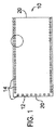
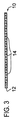
図1および図3を参照すると、本発明の圧電磁歪デバイス10が示されている。デバイスは、圧電材料のシート12を含み、該圧電材料としては、例えば石英、トパーズ、蔗糖、ロッシェル塩、人工水晶等の圧電材料、例えばランガサイト、チタン酸バリウム等のパワーセラミックス、またはポリフッ化ビニリデン(PVDF)等の重合体などである。シート12の長さまたは幅に対する形状または特定のサイズの要件は存在しない。しかしながら、0.1〜200ミリメートル(mm)の長さ、0.1〜200mmの幅であることが好ましい。圧電シート12の厚さは、0.005〜1.0mmの範囲であり得る。
Referring to FIGS. 1 and 3, a piezoelectric
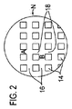
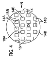
周知のとおり、圧電材料は、適用された機械的応力にさらされた場合に、電位を生成する能力がある。圧電材料のこの性質を活用して、シート12内に穴14の配列が形成され、これらの穴は、磁歪材料によって充填され、磁歪材料は、磁気的エネルギーの変化にさらされた際に長さまたは幅の変化を示すことにより、磁気的エネルギーを機械的エネルギーに変換する。磁歪材料は、コバルト、Terfenol−D、商標名Galfenolの鉄ガリウム合金、NiMnGa等の合金を含み得る。さらに具体的に設計された鉄流体が、デバイス内に応力を含めるように利用され得る。図1は、長手方向の縁部および1つの横方向の縁部のみに沿った穴14を示しているが、穴14は、図2に示されているパターンまたは図4に示されているパターンのいずれかでシート12の実質的に全体にわたり得る。
As is well known, piezoelectric materials are capable of generating an electrical potential when exposed to applied mechanical stress. Taking advantage of this property of the piezoelectric material, an array of
上述したように、圧電材料は、適用された機械的応力に応答して電位を生成する性質を有する。本発明に従うと、上述した材料または類似の性質を有するその他の材料等の磁歪材料を穴14内に配置することにより、機械的歪み等が圧電シート12に選択的に付与され得る。
As described above, piezoelectric materials have the property of generating an electrical potential in response to applied mechanical stress. According to the present invention, a mechanical strain or the like can be selectively imparted to the
図2の実施形態のもとで、任意の形状またはサイズであり得る穴14は、整列された行列内に配置され、その結果、中断を伴わずに、長さ方向に延びる全ての穴14が複数の整列された直線の列のうちの1つの列内に存在し、かつ、横方向に延びる全ての穴14もまた横方向に延びる整列された一連の直線の列のうちの1つの列内に存在する。穴14は、1ナノメートル程度に小さいものであり得、所望に応じて大きいものであり得る。穴14の整列された列の間の空間は、中断を伴わずに、直線経路上でシート12の長さ方向および横方向の両方に延びる。長手方向に整列された穴14の間の空間は、数字16によって示されており、横方向に整列された穴14の間の空間は、数字18によって示されている。
Under the embodiment of FIG. 2, the
図2の実施形態とは対照的に、図4においては、改変された実施形態が示されており、同実施形態においては、穴14の列は、シート12の横方向に延びている穴の列に関して互い違いになった行列を有する。このようにして、図4に明確に見ることができるように、穴14Aは、第1の組の横方向に延びる列を規定し、該第1の組の横方向に延びる列は、互いに平行であり、かつ、互いに離間されている。第2の組の穴14Bは、第2の組の横方向の列を規定し、該第2の組の横方向の列は、互いに平行であり、かつ、互いに離間されているが、穴14によって形成される第1の横方向の列からずれている。
In contrast to the embodiment of FIG. 2, a modified embodiment is shown in FIG. 4, in which the row of
穴14Aの間の横方向の空間は、数字18Aによって示されており、穴14Bの間の横方向の空間は、数字18Bによって示されている。図4の実施形態の互い違いになった行列の穴14A、14Bを配置することの結果として、空間18A、18Bは、横方向の中断されない列(uninterrupted row)を提供しない。このようにして、本実施形態において、穴14Aは、空間18Bの列を中断し、穴14Bは、空間18Aの列を中断する。
The lateral space between the
穴14Aの長手方向の列と穴14Bの長手方向の列との間の長手方向の空間16の列は、中断されない。
The row of
磁歪材料は、穴14の一部または全体に配置され、これには、図4の互い違いになった行列の場合において、穴14A、14Bの両組を含む。穴14内に磁歪材料を有する圧電シート12のデバイス10は、その磁化状態の変化にさらされ、穴14内の磁歪材料は、形状の変化を受け、これにより、歪みが圧電シート12に伸張を付与し、これにより、デバイス10に電力生成を提供することになる。
The magnetostrictive material is disposed in part or all of the
図1に示されているように、電極20が、圧電シート12の対向端部上に搭載される。
As shown in FIG. 1, the
シート12の少なくとも一部の領域において、穴14によって示されているようにシート全体にわたって延びる穴を有するよりもむしろ、シート12の厚さの一部を通るように延びる窪みが存在し得ることもまた、本発明の想定内である。このような窪みの一部または全体は、磁歪材料によって充填され得る。
Rather than having holes extending through the entire sheet as indicated by
圧電シート12は、長方形の形状で図1に示されているが、例えば円形または楕円形等の任意の様々な形状を有し得る。
磁歪材料の特定の形成におけるバリエーションは、デバイス10の性能のキャパシティを変化および/または最大化させるために利用され得る。共振周波数のチューニングは、このような形成を変化させること、ならびに、穴のサイズ、穴の形状または穴の密度を変化させることにより、影響され得る。
Variations in the specific formation of the magnetostrictive material can be utilized to change and / or maximize the performance capacity of the
さらに、図4に示されているような穴の配置の互い違いになった行列は、図2の整列された行列とは異なる性能特性を提供し得る。従って、行列の上述したバリエーション、すなわち穴のサイズ、穴の形状、穴の密度のバリエーションにより、複数の性能特性のうちの任意のものを有するようにデバイスを仕立てることが可能である。 In addition, a staggered matrix of hole arrangements as shown in FIG. 4 may provide different performance characteristics than the aligned matrix of FIG. Thus, a device can be tailored to have any of a plurality of performance characteristics, depending on the above-described variations of the matrix, ie, hole size, hole shape, and hole density variations.
図2に見ることができるように、穴14の整列された行列は、磁化の変化および矢印Nによって示される方向からの磁場に対する露出の際に、穴14内に含まれる磁歪材料の伸張を提供し、これにより、穴14の列の間の横方向の空間18内の文字「A」によって表される領域内のシート12の圧電材料に対する機械的伸張を誘導する。同様に、穴14の 整列された行列は、穴14の列の間の縦方向の空間18内の文字「B」によって表される 領域内のシート12の圧電材料に対する機械的圧縮力を誘導する。
As can be seen in FIG. 2, the aligned matrix of
図4の互い違いになった行列の場合、長手方向に延びる列14A、14Bの間の空間16は、穴14内の磁歪材料の方向Nからの変化に起因して、文字「C」によって示される領域内の伸張を示す。しかしながら、図2の穴の整列とは対照的に、図4の互い違いになった行列においては、穴14Aの間の間の空間18Aは、非整列状態にある、または、開口14Bの間の空間18Bの横方向の配列の外部にある。矢印Nによって示される方向からの磁場を仮定した場合、図4において「C」で示された領域内の空間は、伸張され得、そして、「D」で示された領域内の空間は、圧縮され得る。
In the staggered matrix of FIG. 4, the
容易に理解され得るように、図4に示されている実施形態は、穴の隣接列が互いに対して横方向に整列されるように、穴14A、14Bを配置することを示しているが、穴14の長さ方向の列もまた穴の隣接列と整列されないことは、本発明の想定内である。
As can be readily appreciated, the embodiment shown in FIG. 4 shows placing the
磁歪材料およびその化合物のバリエーションは、特定の用途または所望の性能能力に依存して、デバイス10に対する特性を変化させる結果につながる。デバイス10の共振周波数をチューニングすることは、圧電シート12に対する材料および/または磁歪材料を変化させること、穴14のサイズおよび/または形状を変化させること、穴14の密度またはその他の配置を変化させることにより達成され得る。
Variations in the magnetostrictive material and its compounds can result in changing properties for the
本発明の上述した詳細な実施形態は、例示目的のために与えられている。多くの変更および改変が本発明の範囲を逸脱することなく行われ得ることが、当業者には理解され得る。従って、上述した記載の全体は、例示的な意味で想定され、限定的な意味で想定されるべきではなく、本発明の範囲は、添付の特許請求の範囲のみによって規定されるべきである。 The above detailed embodiments of the present invention are given for illustrative purposes. It will be appreciated by those skilled in the art that many changes and modifications can be made without departing from the scope of the invention. Accordingly, the entirety of the foregoing description is assumed in an illustrative sense and should not be assumed in a limiting sense, and the scope of the present invention should be defined only by the appended claims.
Claims (22)
(a)機械的歪みにさらされた場合に電場を生成する能力を有する圧電材料のシートであって、該シートは、0.005〜1.0mmの範囲の厚さを有し、
(i)第1の表面およびそこから離間され、かつ、それに対して実質的に平行な第2の表面と、
(ii)該第1の表面から該第2の表面に向かって延びている複数の窪みまたは穴であって、該複数の窪みまたは穴は、四角形であり、
(A)複数の列であって、それぞれが、第1の方向における直線経路において延びており、かつ、該第1の方向に延びている各隣接列に平行であり、該第1の方向の列は、複数の平行に整列された空間を規定する各隣接列から離間されている、複数の列と、
(B)複数の列であって、それぞれが、該第1の方向に実質的に垂直な第2の方向に延びている、複数の列とに配置されている、複数の窪みまたは穴と
を有する、圧電材料のシートと、
(b)該複数の窪みまたは穴の少なくとも一部に配置された磁歪材料と
を含む、発電デバイス。 A power generation device,
(A) a sheet of piezoelectric material having the ability to generate an electric field when exposed to mechanical strain, the sheet having a thickness in the range of 0.005 to 1.0 mm;
(I) a first surface and a second surface spaced therefrom and substantially parallel thereto;
(Ii) a plurality of depressions or holes extending from the first surface toward the second surface, wherein the plurality of depressions or holes are square;
(A) a plurality of rows, each extending in a linear path in a first direction and parallel to each adjacent row extending in the first direction, wherein the first direction A plurality of columns spaced from each adjacent column defining a plurality of parallel aligned spaces;
(B) a plurality of depressions or holes, each being arranged in a plurality of rows, each extending in a second direction substantially perpendicular to the first direction. Having a sheet of piezoelectric material;
And (b) a magnetostrictive material disposed in at least a part of the plurality of depressions or holes.
(a)機械的歪みにさらされた場合に電場を生成する能力を有する圧電材料のシートであって、該シートは、0.005〜1.0mmの範囲の厚さを有し、
(i)第1の表面およびそこから離間され、かつ、それに対して実質的に平行な第2
の表面と、
(ii)該第1の表面から該第2の表面に向かって延びている複数の窪みまたは穴と、
(iii)第1の長手方向の縁部および第2の長手方向の縁部と、
(iv)第1の端縁部および第2の端縁部であって、両組の端部は、該第1の表面から該第2の表面まで延びており、該複数の窪みまたは穴は、四角形であり、
(A)複数の長手方向の列であって、それぞれが、該長手方向の縁部に実質的に平行な直線において延びており、該長手方向の列は、隣接する長手方向の列のそれぞれから離間されており、複数の平行に整列された空間を規定しており、該平行な整列された空間は、該長手方向の縁部に対して平行である、複数の長手方向の列と、
(B)複数の横方向の列であって、それぞれが、互いに平行な直線経路において延びている、複数の横方向の列と
に配置されている、第1の端縁部および第2の端縁部と
を有する、圧電材料のシートと、
(b)該複数の窪みまたは穴の少なくとも一部に配置された磁歪材料と
を含む、発電デバイス。 A power generation device,
(A) a sheet of piezoelectric material having the ability to generate an electric field when exposed to mechanical strain, the sheet having a thickness in the range of 0.005 to 1.0 mm;
(I) a first surface and a second spaced apart and substantially parallel thereto
The surface of the
(Ii) a plurality of depressions or holes extending from the first surface toward the second surface;
(Iii) a first longitudinal edge and a second longitudinal edge;
(Iv) a first edge and a second edge, both sets of edges extending from the first surface to the second surface, wherein the plurality of depressions or holes are Is a rectangle,
(A) a plurality of longitudinal rows, each extending in a straight line substantially parallel to the longitudinal edges, the longitudinal rows from each adjacent longitudinal row; A plurality of longitudinal rows spaced apart and defining a plurality of parallel aligned spaces, the parallel aligned spaces being parallel to the longitudinal edges;
(B) a plurality of lateral rows, each arranged in a plurality of lateral rows, each extending in a straight path parallel to each other, the first edge and the second end A sheet of piezoelectric material having an edge; and
(B) a magnetostrictive material disposed in at least a part of the plurality of depressions or holes.
(a)機械的歪みにさらされた場合に電場を生成する能力を有する圧電材料のシートであって、該シートは、0.005〜1.0mmの範囲の厚さを有し、
(i)第1の表面およびそこから離間され、かつ、それに対して実質的に平行な第2の表面と、
(ii)該第1の表面から該第2の表面に向かって延びている複数の窪みまたは穴であって、該複数の窪みまたは穴は、四角形であり、
(A)複数の列であって、それぞれが、第1の方向における直線経路において延びており、かつ、該第1の方向に延びている各隣接列に平行である、複数の列と、
(B)複数の列であって、それぞれが、該第1の方向に実質的に垂直な第2の方向に延びている、複数の列と
に配置されている、複数の窪みまたは穴と
を有する、圧電材料のシートと、
(b)該複数の窪みまたは穴の少なくとも一部に配置された磁歪材料と
を含む、発電デバイス。 A power generation device,
(A) a sheet of piezoelectric material having the ability to generate an electric field when exposed to mechanical strain, the sheet having a thickness in the range of 0.005 to 1.0 mm;
(I) a first surface and a second surface spaced therefrom and substantially parallel thereto;
(Ii) a plurality of depressions or holes extending from the first surface toward the second surface, wherein the plurality of depressions or holes are square;
(A) a plurality of rows, each extending in a linear path in a first direction and parallel to each adjacent row extending in the first direction;
(B) a plurality of depressions or holes arranged in a plurality of rows, each extending in a second direction substantially perpendicular to the first direction. Having a sheet of piezoelectric material;
And (b) a magnetostrictive material disposed in at least a part of the plurality of depressions or holes.
た行列からなる、請求項9に記載の発電デバイス。 The power generation device according to claim 9, wherein the plurality of columns extending in the first direction are formed of a matrix in which the depressions or holes are alternately arranged.
(a)機械的歪みにさらされた場合に電場を生成する能力を有する圧電材料のシートを提供するステップであって、該シートは、0.005〜1.0mmの範囲の厚さを有し、第1の表面およびそこから離間され、かつ、それに対して実質的に平行な第2の表面を有する、ステップと、
(b)第1の表面から第2の表面まで延びている該シート内に複数の窪みまたは穴を形成するステップであって、該複数の窪みまたは穴は、四角形であり、
(i)複数の列であって、それぞれが、第1の方向における直線経路において延びており、かつ、該第1の方向に延びている各隣接列に平行である、複数の列と、
(ii)複数の列であって、それぞれが、該第1の方向に対して実質的に垂直な第2の方向に延びている、複数の列と
に配置されている、ステップと、
(c)該複数の窪みまたは穴の少なくとも一部に磁歪材料を配置するステップと、
(d)ステップ(c)に記載の配置の時点で磁場が存在する場合に、該磁場とは異なる磁場に該圧電材料のシートおよび該磁歪材料をさらすステップと
を含む、発電デバイスの製造方法。 A method for manufacturing a power generation device, comprising:
(A) providing a sheet of piezoelectric material having the ability to generate an electric field when exposed to mechanical strain, the sheet having a thickness in the range of 0.005 to 1.0 mm; Having a first surface and a second surface spaced therefrom and substantially parallel thereto;
(B) forming a plurality of depressions or holes in the sheet extending from the first surface to the second surface, wherein the plurality of depressions or holes are square;
A (i) a plurality of rows, each of which extends in a straight path in a first direction, and is parallel to each adjacent row extending in the first direction, and a plurality of columns,
(Ii) a plurality of rows, each arranged in a plurality of rows extending in a second direction substantially perpendicular to the first direction; and
(C) disposing a magnetostrictive material in at least a portion of the plurality of depressions or holes;
(D) when a magnetic field exists at the time of the arrangement described in step (c), exposing the sheet of piezoelectric material and the magnetostrictive material to a magnetic field different from the magnetic field.
Applications Claiming Priority (3)
| Application Number | Priority Date | Filing Date | Title |
|---|---|---|---|
| US27008009P | 2009-07-02 | 2009-07-02 | |
| US61/270,080 | 2009-07-02 | ||
| PCT/US2010/001885 WO2011002514A1 (en) | 2009-07-02 | 2010-07-01 | Piezo magnetostrictive device |
Publications (2)
| Publication Number | Publication Date |
|---|---|
| JP2012532579A JP2012532579A (en) | 2012-12-13 |
| JP5750439B2 true JP5750439B2 (en) | 2015-07-22 |
Family
ID=43411346
Family Applications (1)
| Application Number | Title | Priority Date | Filing Date |
|---|---|---|---|
| JP2012518527A Expired - Fee Related JP5750439B2 (en) | 2009-07-02 | 2010-07-01 | Piezoelectric strain device |
Country Status (8)
| Country | Link |
|---|---|
| US (1) | US8330335B2 (en) |
| EP (1) | EP2449610B1 (en) |
| JP (1) | JP5750439B2 (en) |
| KR (1) | KR101337067B1 (en) |
| CA (1) | CA2760797A1 (en) |
| ES (1) | ES2659887T3 (en) |
| MX (1) | MX2011012847A (en) |
| WO (1) | WO2011002514A1 (en) |
Families Citing this family (5)
| Publication number | Priority date | Publication date | Assignee | Title |
|---|---|---|---|---|
| US8432086B2 (en) * | 2010-02-02 | 2013-04-30 | Cooper Tire & Rubber Company | Ferro fluid for inducing linear stress |
| WO2014113694A1 (en) * | 2013-01-17 | 2014-07-24 | Northeastern University | Magnetoelectric pickup element for detecting oscillating magnetic fields |
| EP3117195B1 (en) * | 2014-03-10 | 2019-11-06 | Qortek, Inc. | Non-contact magnetostrictive current sensor |
| US9524709B2 (en) * | 2014-10-21 | 2016-12-20 | The Regents Of The University Of California | Multiferroic transducer for audio applications |
| CN109963063B (en) * | 2019-04-02 | 2021-03-19 | Oppo广东移动通信有限公司 | Adjusting structure, camera and terminal equipment |
Family Cites Families (21)
| Publication number | Priority date | Publication date | Assignee | Title |
|---|---|---|---|---|
| JPS5544730A (en) * | 1978-09-27 | 1980-03-29 | Toshiba Corp | Electric machine transducer |
| JPS5617088A (en) * | 1979-07-20 | 1981-02-18 | Matsushita Electric Ind Co Ltd | Manufacture of magnetoelectricity converting element |
| US5473938A (en) | 1993-08-03 | 1995-12-12 | Mclaughlin Electronics | Method and system for monitoring a parameter of a vehicle tire |
| US5500065A (en) | 1994-06-03 | 1996-03-19 | Bridgestone/Firestone, Inc. | Method for embedding a monitoring device within a tire during manufacture |
| US6062072A (en) | 1995-08-11 | 2000-05-16 | Dynatron Ag | Device for monitoring the air pressure of pneumatic tires of vehicles |
| JPH0965221A (en) * | 1995-08-24 | 1997-03-07 | Sony Corp | Imaging device |
| EP1097049B1 (en) * | 1998-07-10 | 2003-09-03 | The Goodyear Tire & Rubber Company | Self-powered tire revolution counter |
| JP2000088937A (en) * | 1998-09-17 | 2000-03-31 | Ngk Insulators Ltd | Magnetic field sensor and current detector using the same |
| AU3353300A (en) * | 1999-04-05 | 2000-10-23 | Spinix Corporation | Passive solid-state magnetic field sensors and applications therefor |
| US6362731B1 (en) | 2000-12-06 | 2002-03-26 | Eaton Corporation | Tire pressure monitor and location identification system and method |
| US6798331B2 (en) * | 2001-02-08 | 2004-09-28 | Qortek, Inc. | Current control device |
| CN1589457B (en) | 2001-12-21 | 2010-05-12 | 德国捷德有限公司 | Sheet material and apparatus and method for manufacturing and processing the same |
| US7009576B2 (en) | 2002-06-11 | 2006-03-07 | Michelin Recherche Et Technique S.A. | Radio frequency antenna for a tire and method for same |
| JP2005012980A (en) * | 2003-06-23 | 2005-01-13 | Casio Comput Co Ltd | Charger |
| US6856245B2 (en) | 2003-07-09 | 2005-02-15 | Julian Smith | Tire condition monitoring system with improved sensor means |
| JP4052290B2 (en) | 2003-08-29 | 2008-02-27 | オムロン株式会社 | Wireless IC tag joining method, article with wireless IC tag, and vehicle |
| US7186308B2 (en) | 2003-10-09 | 2007-03-06 | Michelin Recherche Et Technique S.A. | System and method for providing tire electronics mounting patches |
| JP2005156182A (en) * | 2003-11-20 | 2005-06-16 | Toshiba Corp | Magnetic field detection device using magnetic field sensor |
| US7132939B2 (en) | 2004-07-07 | 2006-11-07 | Michelin Recherche Et Technique S.A. | Integrated self-powered tire revolution counter |
| US7645246B2 (en) | 2004-08-11 | 2010-01-12 | Omnitek Partners Llc | Method for generating power across a joint of the body during a locomotion cycle |
| CA2605850C (en) | 2005-04-26 | 2012-03-13 | Cooper Tire & Rubber Company | Rfid transmitter for tires and method of manufacture |
-
2010
- 2010-07-01 US US12/803,644 patent/US8330335B2/en not_active Expired - Fee Related
- 2010-07-01 EP EP10794493.6A patent/EP2449610B1/en not_active Not-in-force
- 2010-07-01 CA CA2760797A patent/CA2760797A1/en not_active Abandoned
- 2010-07-01 JP JP2012518527A patent/JP5750439B2/en not_active Expired - Fee Related
- 2010-07-01 ES ES10794493.6T patent/ES2659887T3/en active Active
- 2010-07-01 WO PCT/US2010/001885 patent/WO2011002514A1/en not_active Ceased
- 2010-07-01 KR KR1020117027938A patent/KR101337067B1/en not_active Expired - Fee Related
- 2010-07-01 MX MX2011012847A patent/MX2011012847A/en active IP Right Grant
Also Published As
| Publication number | Publication date |
|---|---|
| MX2011012847A (en) | 2012-01-12 |
| CA2760797A1 (en) | 2011-01-06 |
| WO2011002514A1 (en) | 2011-01-06 |
| US20110001397A1 (en) | 2011-01-06 |
| US8330335B2 (en) | 2012-12-11 |
| EP2449610A4 (en) | 2013-08-14 |
| KR101337067B1 (en) | 2013-12-05 |
| EP2449610A1 (en) | 2012-05-09 |
| ES2659887T3 (en) | 2018-03-19 |
| KR20120025482A (en) | 2012-03-15 |
| EP2449610B1 (en) | 2018-01-10 |
| JP2012532579A (en) | 2012-12-13 |
Similar Documents
| Publication | Publication Date | Title |
|---|---|---|
| JP5750439B2 (en) | Piezoelectric strain device | |
| Farhangdoust et al. | Kirigami auxetic structure for high efficiency power harvesting in self-powered and wireless structural health monitoring systems | |
| Silva et al. | Optimization of the magnetoelectric response of poly (vinylidene fluoride)/epoxy/vitrovac laminates | |
| US9876161B2 (en) | Method of fabricating piezoelectric energy harvesting device | |
| TW200746237A (en) | Method for making an electronic device including a poled superlattice having a net electrical dipole moment | |
| KR102339058B1 (en) | Flexible piezoelectric composite and piezoelectric device including the same | |
| JP2015537439A5 (en) | ||
| US8446077B2 (en) | 3-D woven active fiber composite | |
| Talib et al. | Comprehensive review on effective strategies and key factors for high performance piezoelectric energy harvester at low frequency | |
| Schäffner et al. | Microstructured single-layer electrodes embedded in P (VDF-TrFE) for flexible and self-powered direction-sensitive strain sensors | |
| CN105790634B (en) | A kind of wideband acoustic energy retracting device | |
| US20160276959A1 (en) | Converter for converting energy to be recovered and electricity generator | |
| KR101286714B1 (en) | Piezoelectric energy harvesting device | |
| US8432086B2 (en) | Ferro fluid for inducing linear stress | |
| US20140185840A1 (en) | Thermoacoustic device | |
| EP1689080A3 (en) | Film bulk acoustic resonator and a method for manufacturing the same | |
| KR20160139532A (en) | Energy converting device using flexoelectric effect | |
| Kang et al. | Energy harvesting using ferroelectric/ferroelastic switching: the effect of pre-poling | |
| JP2010226609A5 (en) | ||
| US20040183406A1 (en) | Piezoelectrical bending converter | |
| Wang et al. | Characteristic analysis of novel double-fork piezoelectric energy harvester | |
| EP4120372B1 (en) | Magnetoelectric voltage transformer device | |
| Devi et al. | Understanding the enhanced piezoelectric response in inclined ZnO nanorods | |
| KR101841840B1 (en) | Layered piezoelectric element | |
| JP4408721B2 (en) | Drive device |
Legal Events
| Date | Code | Title | Description |
|---|---|---|---|
| RD03 | Notification of appointment of power of attorney |
Free format text: JAPANESE INTERMEDIATE CODE: A7423 Effective date: 20121004 |
|
| RD04 | Notification of resignation of power of attorney |
Free format text: JAPANESE INTERMEDIATE CODE: A7424 Effective date: 20121012 |
|
| A621 | Written request for application examination |
Free format text: JAPANESE INTERMEDIATE CODE: A621 Effective date: 20130701 |
|
| A977 | Report on retrieval |
Free format text: JAPANESE INTERMEDIATE CODE: A971007 Effective date: 20140625 |
|
| A131 | Notification of reasons for refusal |
Free format text: JAPANESE INTERMEDIATE CODE: A131 Effective date: 20140701 |
|
| A601 | Written request for extension of time |
Free format text: JAPANESE INTERMEDIATE CODE: A601 Effective date: 20140930 |
|
| A602 | Written permission of extension of time |
Free format text: JAPANESE INTERMEDIATE CODE: A602 Effective date: 20141007 |
|
| A521 | Request for written amendment filed |
Free format text: JAPANESE INTERMEDIATE CODE: A523 Effective date: 20141024 |
|
| A131 | Notification of reasons for refusal |
Free format text: JAPANESE INTERMEDIATE CODE: A131 Effective date: 20141202 |
|
| A521 | Request for written amendment filed |
Free format text: JAPANESE INTERMEDIATE CODE: A523 Effective date: 20150302 |
|
| TRDD | Decision of grant or rejection written | ||
| A01 | Written decision to grant a patent or to grant a registration (utility model) |
Free format text: JAPANESE INTERMEDIATE CODE: A01 Effective date: 20150324 |
|
| A601 | Written request for extension of time |
Free format text: JAPANESE INTERMEDIATE CODE: A601 Effective date: 20150422 |
|
| A61 | First payment of annual fees (during grant procedure) |
Free format text: JAPANESE INTERMEDIATE CODE: A61 Effective date: 20150518 |
|
| R150 | Certificate of patent or registration of utility model |
Ref document number: 5750439 Country of ref document: JP Free format text: JAPANESE INTERMEDIATE CODE: R150 |
|
| R250 | Receipt of annual fees |
Free format text: JAPANESE INTERMEDIATE CODE: R250 |
|
| R250 | Receipt of annual fees |
Free format text: JAPANESE INTERMEDIATE CODE: R250 |
|
| R250 | Receipt of annual fees |
Free format text: JAPANESE INTERMEDIATE CODE: R250 |
|
| R250 | Receipt of annual fees |
Free format text: JAPANESE INTERMEDIATE CODE: R250 |
|
| R250 | Receipt of annual fees |
Free format text: JAPANESE INTERMEDIATE CODE: R250 |
|
| S111 | Request for change of ownership or part of ownership |
Free format text: JAPANESE INTERMEDIATE CODE: R313113 |
|
| R350 | Written notification of registration of transfer |
Free format text: JAPANESE INTERMEDIATE CODE: R350 |
|
| LAPS | Cancellation because of no payment of annual fees |