JP5744941B2 - Radiographic image detection apparatus and radiographic imaging system - Google Patents
Radiographic image detection apparatus and radiographic imaging system Download PDFInfo
- Publication number
- JP5744941B2 JP5744941B2 JP2013045386A JP2013045386A JP5744941B2 JP 5744941 B2 JP5744941 B2 JP 5744941B2 JP 2013045386 A JP2013045386 A JP 2013045386A JP 2013045386 A JP2013045386 A JP 2013045386A JP 5744941 B2 JP5744941 B2 JP 5744941B2
- Authority
- JP
- Japan
- Prior art keywords
- wavelength conversion
- conversion layer
- phosphor
- layer
- image detection
- Prior art date
- Legal status (The legal status is an assumption and is not a legal conclusion. Google has not performed a legal analysis and makes no representation as to the accuracy of the status listed.)
- Active
Links
- 238000001514 detection method Methods 0.000 title claims description 50
- 238000003384 imaging method Methods 0.000 title claims description 11
- 239000010410 layer Substances 0.000 claims description 214
- 239000002245 particle Substances 0.000 claims description 213
- OAICVXFJPJFONN-UHFFFAOYSA-N Phosphorus Chemical compound [P] OAICVXFJPJFONN-UHFFFAOYSA-N 0.000 claims description 200
- 238000006243 chemical reaction Methods 0.000 claims description 153
- 239000007787 solid Substances 0.000 claims description 81
- 230000005855 radiation Effects 0.000 claims description 78
- 239000011230 binding agent Substances 0.000 claims description 42
- 239000011248 coating agent Substances 0.000 claims description 42
- 238000000576 coating method Methods 0.000 claims description 42
- 238000011049 filling Methods 0.000 claims description 25
- 239000007767 bonding agent Substances 0.000 claims description 19
- 238000001035 drying Methods 0.000 claims description 14
- 230000007423 decrease Effects 0.000 claims description 11
- 230000002093 peripheral effect Effects 0.000 claims description 6
- 230000006835 compression Effects 0.000 claims description 5
- 238000007906 compression Methods 0.000 claims description 5
- 239000002356 single layer Substances 0.000 claims description 5
- 229910052693 Europium Inorganic materials 0.000 claims description 3
- 229910052688 Gadolinium Inorganic materials 0.000 claims description 3
- 229910052765 Lutetium Inorganic materials 0.000 claims description 3
- 229910052777 Praseodymium Inorganic materials 0.000 claims description 3
- 229910052771 Terbium Inorganic materials 0.000 claims description 3
- 229910052746 lanthanum Inorganic materials 0.000 claims description 3
- 229910052727 yttrium Inorganic materials 0.000 claims description 3
- 238000000926 separation method Methods 0.000 claims 1
- ZWEHNKRNPOVVGH-UHFFFAOYSA-N 2-Butanone Chemical compound CCC(C)=O ZWEHNKRNPOVVGH-UHFFFAOYSA-N 0.000 description 24
- 239000007788 liquid Substances 0.000 description 17
- 229920005989 resin Polymers 0.000 description 15
- 239000011347 resin Substances 0.000 description 15
- 230000035945 sensitivity Effects 0.000 description 14
- 239000000463 material Substances 0.000 description 12
- 238000004519 manufacturing process Methods 0.000 description 10
- 229920000139 polyethylene terephthalate Polymers 0.000 description 9
- 239000005020 polyethylene terephthalate Substances 0.000 description 9
- 239000005056 polyisocyanate Substances 0.000 description 9
- 229920001228 polyisocyanate Polymers 0.000 description 9
- 229920000642 polymer Polymers 0.000 description 9
- 239000003795 chemical substances by application Substances 0.000 description 8
- -1 polysiloxane unit Polymers 0.000 description 8
- 239000000203 mixture Substances 0.000 description 7
- 239000011241 protective layer Substances 0.000 description 7
- 239000000126 substance Substances 0.000 description 7
- YXFVVABEGXRONW-UHFFFAOYSA-N Toluene Chemical compound CC1=CC=CC=C1 YXFVVABEGXRONW-UHFFFAOYSA-N 0.000 description 6
- 230000015572 biosynthetic process Effects 0.000 description 6
- 238000000034 method Methods 0.000 description 6
- 229920001296 polysiloxane Polymers 0.000 description 5
- 239000002904 solvent Substances 0.000 description 5
- 239000013078 crystal Substances 0.000 description 4
- 238000009826 distribution Methods 0.000 description 4
- 239000010419 fine particle Substances 0.000 description 4
- 229920000728 polyester Polymers 0.000 description 4
- DVKJHBMWWAPEIU-UHFFFAOYSA-N toluene 2,4-diisocyanate Chemical compound CC1=CC=C(N=C=O)C=C1N=C=O DVKJHBMWWAPEIU-UHFFFAOYSA-N 0.000 description 4
- 229910006404 SnO 2 Inorganic materials 0.000 description 3
- BTANRVKWQNVYAZ-UHFFFAOYSA-N butan-2-ol Chemical compound CCC(C)O BTANRVKWQNVYAZ-UHFFFAOYSA-N 0.000 description 3
- 230000008859 change Effects 0.000 description 3
- 230000003247 decreasing effect Effects 0.000 description 3
- 239000000428 dust Substances 0.000 description 3
- 239000000178 monomer Substances 0.000 description 3
- 239000004094 surface-active agent Substances 0.000 description 3
- 239000004925 Acrylic resin Substances 0.000 description 2
- 229920000178 Acrylic resin Polymers 0.000 description 2
- CTQNGGLPUBDAKN-UHFFFAOYSA-N O-Xylene Chemical compound CC1=CC=CC=C1C CTQNGGLPUBDAKN-UHFFFAOYSA-N 0.000 description 2
- 239000004820 Pressure-sensitive adhesive Substances 0.000 description 2
- ZJCCRDAZUWHFQH-UHFFFAOYSA-N Trimethylolpropane Chemical compound CCC(CO)(CO)CO ZJCCRDAZUWHFQH-UHFFFAOYSA-N 0.000 description 2
- NIXOWILDQLNWCW-UHFFFAOYSA-N acrylic acid group Chemical group C(C=C)(=O)O NIXOWILDQLNWCW-UHFFFAOYSA-N 0.000 description 2
- PNEYBMLMFCGWSK-UHFFFAOYSA-N aluminium oxide Inorganic materials [O-2].[O-2].[O-2].[Al+3].[Al+3] PNEYBMLMFCGWSK-UHFFFAOYSA-N 0.000 description 2
- 239000006258 conductive agent Substances 0.000 description 2
- RRAMGCGOFNQTLD-UHFFFAOYSA-N hexamethylene diisocyanate Chemical compound O=C=NCCCCCCN=C=O RRAMGCGOFNQTLD-UHFFFAOYSA-N 0.000 description 2
- 125000002887 hydroxy group Chemical group [H]O* 0.000 description 2
- 239000012948 isocyanate Substances 0.000 description 2
- 150000002513 isocyanates Chemical class 0.000 description 2
- 238000010030 laminating Methods 0.000 description 2
- 238000002156 mixing Methods 0.000 description 2
- 239000004814 polyurethane Substances 0.000 description 2
- 229920002635 polyurethane Polymers 0.000 description 2
- 230000008569 process Effects 0.000 description 2
- 230000001902 propagating effect Effects 0.000 description 2
- 230000009467 reduction Effects 0.000 description 2
- 239000013557 residual solvent Substances 0.000 description 2
- 230000004044 response Effects 0.000 description 2
- 239000004065 semiconductor Substances 0.000 description 2
- 229920005573 silicon-containing polymer Polymers 0.000 description 2
- 239000002344 surface layer Substances 0.000 description 2
- 239000008096 xylene Substances 0.000 description 2
- VZSRBBMJRBPUNF-UHFFFAOYSA-N 2-(2,3-dihydro-1H-inden-2-ylamino)-N-[3-oxo-3-(2,4,6,7-tetrahydrotriazolo[4,5-c]pyridin-5-yl)propyl]pyrimidine-5-carboxamide Chemical compound C1C(CC2=CC=CC=C12)NC1=NC=C(C=N1)C(=O)NCCC(N1CC2=C(CC1)NN=N2)=O VZSRBBMJRBPUNF-UHFFFAOYSA-N 0.000 description 1
- XMWRBQBLMFGWIX-UHFFFAOYSA-N C60 fullerene Chemical compound C12=C3C(C4=C56)=C7C8=C5C5=C9C%10=C6C6=C4C1=C1C4=C6C6=C%10C%10=C9C9=C%11C5=C8C5=C8C7=C3C3=C7C2=C1C1=C2C4=C6C4=C%10C6=C9C9=C%11C5=C5C8=C3C3=C7C1=C1C2=C4C6=C2C9=C5C3=C12 XMWRBQBLMFGWIX-UHFFFAOYSA-N 0.000 description 1
- OKTJSMMVPCPJKN-UHFFFAOYSA-N Carbon Chemical compound [C] OKTJSMMVPCPJKN-UHFFFAOYSA-N 0.000 description 1
- 229910052684 Cerium Inorganic materials 0.000 description 1
- 239000005057 Hexamethylene diisocyanate Substances 0.000 description 1
- 239000004952 Polyamide Substances 0.000 description 1
- 239000004642 Polyimide Substances 0.000 description 1
- 239000004721 Polyphenylene oxide Substances 0.000 description 1
- 229920002396 Polyurea Polymers 0.000 description 1
- 229910052772 Samarium Inorganic materials 0.000 description 1
- BUGBHKTXTAQXES-UHFFFAOYSA-N Selenium Chemical compound [Se] BUGBHKTXTAQXES-UHFFFAOYSA-N 0.000 description 1
- 239000003522 acrylic cement Substances 0.000 description 1
- 238000004458 analytical method Methods 0.000 description 1
- 238000000149 argon plasma sintering Methods 0.000 description 1
- 230000004888 barrier function Effects 0.000 description 1
- 230000000903 blocking effect Effects 0.000 description 1
- 150000001721 carbon Chemical class 0.000 description 1
- 239000006229 carbon black Substances 0.000 description 1
- 239000002041 carbon nanotube Substances 0.000 description 1
- 229910021393 carbon nanotube Inorganic materials 0.000 description 1
- 229920002301 cellulose acetate Polymers 0.000 description 1
- GWXLDORMOJMVQZ-UHFFFAOYSA-N cerium Chemical compound [Ce] GWXLDORMOJMVQZ-UHFFFAOYSA-N 0.000 description 1
- 230000003081 coactivator Effects 0.000 description 1
- 150000001875 compounds Chemical class 0.000 description 1
- 238000006482 condensation reaction Methods 0.000 description 1
- 239000000470 constituent Substances 0.000 description 1
- 238000003851 corona treatment Methods 0.000 description 1
- 239000003431 cross linking reagent Substances 0.000 description 1
- 238000005520 cutting process Methods 0.000 description 1
- 239000000539 dimer Substances 0.000 description 1
- 239000006185 dispersion Substances 0.000 description 1
- 239000003822 epoxy resin Substances 0.000 description 1
- 229910003472 fullerene Inorganic materials 0.000 description 1
- 230000005484 gravity Effects 0.000 description 1
- 230000001678 irradiating effect Effects 0.000 description 1
- 238000002844 melting Methods 0.000 description 1
- 230000008018 melting Effects 0.000 description 1
- 239000012046 mixed solvent Substances 0.000 description 1
- 230000001151 other effect Effects 0.000 description 1
- 239000004014 plasticizer Substances 0.000 description 1
- 229920002037 poly(vinyl butyral) polymer Polymers 0.000 description 1
- 229920002647 polyamide Polymers 0.000 description 1
- 229920000515 polycarbonate Polymers 0.000 description 1
- 239000004417 polycarbonate Substances 0.000 description 1
- 229920000647 polyepoxide Polymers 0.000 description 1
- 229920001225 polyester resin Polymers 0.000 description 1
- 239000004645 polyester resin Substances 0.000 description 1
- 229920000570 polyether Polymers 0.000 description 1
- 229920001721 polyimide Polymers 0.000 description 1
- 229920005862 polyol Polymers 0.000 description 1
- 150000003077 polyols Chemical class 0.000 description 1
- 230000000630 rising effect Effects 0.000 description 1
- KZUNJOHGWZRPMI-UHFFFAOYSA-N samarium atom Chemical compound [Sm] KZUNJOHGWZRPMI-UHFFFAOYSA-N 0.000 description 1
- 238000005070 sampling Methods 0.000 description 1
- 229920006395 saturated elastomer Polymers 0.000 description 1
- 229910052711 selenium Inorganic materials 0.000 description 1
- 239000011669 selenium Substances 0.000 description 1
- 229920002803 thermoplastic polyurethane Polymers 0.000 description 1
- ILJSQTXMGCGYMG-UHFFFAOYSA-N triacetic acid Chemical compound CC(=O)CC(=O)CC(O)=O ILJSQTXMGCGYMG-UHFFFAOYSA-N 0.000 description 1
- 239000013638 trimer Substances 0.000 description 1
- 238000004394 yellowing prevention Methods 0.000 description 1
Images


Classifications
-
- G—PHYSICS
- G01—MEASURING; TESTING
- G01T—MEASUREMENT OF NUCLEAR OR X-RADIATION
- G01T1/00—Measuring X-radiation, gamma radiation, corpuscular radiation, or cosmic radiation
- G01T1/16—Measuring radiation intensity
- G01T1/20—Measuring radiation intensity with scintillation detectors
- G01T1/2012—Measuring radiation intensity with scintillation detectors using stimulable phosphors, e.g. stimulable phosphor sheets
-
- A—HUMAN NECESSITIES
- A61—MEDICAL OR VETERINARY SCIENCE; HYGIENE
- A61B—DIAGNOSIS; SURGERY; IDENTIFICATION
- A61B6/00—Apparatus for radiation diagnosis, e.g. combined with radiation therapy equipment
- A61B6/42—Apparatus for radiation diagnosis, e.g. combined with radiation therapy equipment with arrangements for detecting radiation specially adapted for radiation diagnosis
- A61B6/4208—Apparatus for radiation diagnosis, e.g. combined with radiation therapy equipment with arrangements for detecting radiation specially adapted for radiation diagnosis characterised by using a particular type of detector
- A61B6/4216—Apparatus for radiation diagnosis, e.g. combined with radiation therapy equipment with arrangements for detecting radiation specially adapted for radiation diagnosis characterised by using a particular type of detector using storage phosphor screens
-
- C—CHEMISTRY; METALLURGY
- C09—DYES; PAINTS; POLISHES; NATURAL RESINS; ADHESIVES; COMPOSITIONS NOT OTHERWISE PROVIDED FOR; APPLICATIONS OF MATERIALS NOT OTHERWISE PROVIDED FOR
- C09K—MATERIALS FOR MISCELLANEOUS APPLICATIONS, NOT PROVIDED FOR ELSEWHERE
- C09K11/00—Luminescent, e.g. electroluminescent, chemiluminescent materials
- C09K11/08—Luminescent, e.g. electroluminescent, chemiluminescent materials containing inorganic luminescent materials
- C09K11/77—Luminescent, e.g. electroluminescent, chemiluminescent materials containing inorganic luminescent materials containing rare earth metals
- C09K11/7766—Luminescent, e.g. electroluminescent, chemiluminescent materials containing inorganic luminescent materials containing rare earth metals containing two or more rare earth metals
- C09K11/7767—Chalcogenides
- C09K11/7769—Oxides
- C09K11/7771—Oxysulfides
-
- G—PHYSICS
- G01—MEASURING; TESTING
- G01T—MEASUREMENT OF NUCLEAR OR X-RADIATION
- G01T1/00—Measuring X-radiation, gamma radiation, corpuscular radiation, or cosmic radiation
- G01T1/16—Measuring radiation intensity
- G01T1/20—Measuring radiation intensity with scintillation detectors
- G01T1/2008—Measuring radiation intensity with scintillation detectors using a combination of different types of scintillation detectors, e.g. phoswich
-
- G—PHYSICS
- G01—MEASURING; TESTING
- G01T—MEASUREMENT OF NUCLEAR OR X-RADIATION
- G01T1/00—Measuring X-radiation, gamma radiation, corpuscular radiation, or cosmic radiation
- G01T1/16—Measuring radiation intensity
- G01T1/20—Measuring radiation intensity with scintillation detectors
- G01T1/2018—Scintillation-photodiode combinations
- G01T1/20186—Position of the photodiode with respect to the incoming radiation, e.g. in the front of, below or sideways the scintillator
-
- G—PHYSICS
- G01—MEASURING; TESTING
- G01T—MEASUREMENT OF NUCLEAR OR X-RADIATION
- G01T1/00—Measuring X-radiation, gamma radiation, corpuscular radiation, or cosmic radiation
- G01T1/16—Measuring radiation intensity
- G01T1/20—Measuring radiation intensity with scintillation detectors
- G01T1/2018—Scintillation-photodiode combinations
- G01T1/20187—Position of the scintillator with respect to the photodiode, e.g. photodiode surrounding the crystal, the crystal surrounding the photodiode, shape or size of the scintillator
-
- G—PHYSICS
- G21—NUCLEAR PHYSICS; NUCLEAR ENGINEERING
- G21K—TECHNIQUES FOR HANDLING PARTICLES OR IONISING RADIATION NOT OTHERWISE PROVIDED FOR; IRRADIATION DEVICES; GAMMA RAY OR X-RAY MICROSCOPES
- G21K4/00—Conversion screens for the conversion of the spatial distribution of X-rays or particle radiation into visible images, e.g. fluoroscopic screens
Landscapes
- Life Sciences & Earth Sciences (AREA)
- Health & Medical Sciences (AREA)
- Physics & Mathematics (AREA)
- High Energy & Nuclear Physics (AREA)
- Molecular Biology (AREA)
- Chemical & Material Sciences (AREA)
- Spectroscopy & Molecular Physics (AREA)
- General Physics & Mathematics (AREA)
- Engineering & Computer Science (AREA)
- Medical Informatics (AREA)
- General Engineering & Computer Science (AREA)
- Organic Chemistry (AREA)
- Materials Engineering (AREA)
- Inorganic Chemistry (AREA)
- Crystallography & Structural Chemistry (AREA)
- Radiology & Medical Imaging (AREA)
- Optics & Photonics (AREA)
- Pathology (AREA)
- Nuclear Medicine, Radiotherapy & Molecular Imaging (AREA)
- Biomedical Technology (AREA)
- Heart & Thoracic Surgery (AREA)
- Surgery (AREA)
- Animal Behavior & Ethology (AREA)
- General Health & Medical Sciences (AREA)
- Public Health (AREA)
- Veterinary Medicine (AREA)
- Biophysics (AREA)
- Measurement Of Radiation (AREA)
Description
本発明は、放射線を波長変換層(蛍光体層)により光に変換して放射線画像を検出する放射線画像検出装置及び放射線画像撮影システムに関する。 The present invention relates to a radiographic image detection apparatus and a radiographic imaging system that detect a radiographic image by converting radiation into light by a wavelength conversion layer (phosphor layer).
医療分野などにおいて、被写体にX線などの放射線を照射し、被写体を透過した放射線を検出することにより被写体の放射線画像を検出する放射線画像検出装置が各種実用化されている。このような放射線画像検出装置として、放射線の入射に応じて電荷を生成し、この電荷を電圧に変換して放射線画像を表す画像データを生成する電気読取方式のものが普及している。 In the medical field and the like, various radiological image detection apparatuses that detect a radiographic image of a subject by irradiating the subject with radiation such as X-rays and detecting the radiation transmitted through the subject have been put into practical use. As such a radiographic image detection apparatus, an electric reading type apparatus that generates electric charges in response to incidence of radiation and converts the electric charges into a voltage to generate image data representing a radiographic image is widely used.
この電気読取方式の放射線画像検出装置としては、放射線をセレン等の半導体層により直接電荷に変換する直接変換方式のものや、放射線を波長変換層により一旦光に変換し、その光を、フォトダイオードなどを有する固体検出器によって電荷に変換する間接変換方式のものがある。 As an electric reading type radiological image detection apparatus, a direct conversion type that directly converts radiation into a charge by a semiconductor layer such as selenium, or once converted from radiation to light by a wavelength conversion layer, the light is converted into a photodiode. There is an indirect conversion type in which the charge is converted into a charge by a solid state detector having the above.
間接変換方式の放射線画像検出装置では、波長変換層と固体検出器とが積層されている。波長変換層では、放射線の入射に応じて可視光の発光が生じるが、その発光は、主として放射線が入射した表層で生じる。このため、波長変換層側から放射線画像検出装置に放射線を入射した場合には、波長変換層の表層で生じた光が固体検出器に向かって伝播する間に、その一部がその波長変換層自身によって吸収されて感度が低下するという問題や、波長変換層内での光の散乱により画像にボケが生じ鮮鋭度が低下するという問題がある。 In the indirect conversion type radiological image detection apparatus, a wavelength conversion layer and a solid state detector are laminated. In the wavelength conversion layer, visible light emission is generated in response to the incidence of radiation, but the light emission mainly occurs in the surface layer on which the radiation is incident. For this reason, when radiation is incident on the radiation image detection device from the wavelength conversion layer side, a part of the light is generated in the surface layer of the wavelength conversion layer while propagating toward the solid state detector. There is a problem that the sensitivity is reduced by being absorbed by itself, and there is a problem that the image is blurred due to light scattering in the wavelength conversion layer and the sharpness is lowered.
そこで、特許文献1などにおいて、波長変換層とは反対の固体検出器側から放射線を入射させ、固体検出器を透過した放射線を波長変換層で光に変換することが提案されている。この場合、波長変換層での発光が波長変換層内の固体検出器側の近傍で主に生じるため、上記のような感度や鮮鋭度の低下が抑えられる。このような方式は、放射線の照射側に固体検出器を配置することから、ISS(Irradiation Side Sampling)方式と呼ばれている。 Therefore, in Patent Document 1 or the like, it is proposed that radiation is incident from the side of the solid detector opposite to the wavelength conversion layer, and the radiation transmitted through the solid detector is converted into light by the wavelength conversion layer. In this case, since light emission in the wavelength conversion layer mainly occurs in the vicinity of the solid-state detector side in the wavelength conversion layer, the above-described decrease in sensitivity and sharpness can be suppressed. Such a system is called an ISS (Irradiation Side Sampling) system because a solid state detector is arranged on the radiation irradiation side.
波長変換層は、放射線を可視光に変換する蛍光体を含む。この蛍光体は、GOS(Gd2O2S:Tb)等の粒子(以下、蛍光体粒子という)や、CsI:Tlなどの柱状結晶である。粒子構造の波長変換層は、柱状結晶構造の波長変換層と比べて製造が容易であり安価であることから、広く用いられている。粒子構造の波長変換層は、蛍光体粒子を樹脂などのバインダ(結合剤)に分散させたものである。 The wavelength conversion layer includes a phosphor that converts radiation into visible light. The phosphor is a particle such as GOS (Gd 2 O 2 S: Tb) (hereinafter referred to as phosphor particle) or a columnar crystal such as CsI: Tl. A wavelength conversion layer having a particle structure is widely used because it is easier to manufacture and cheaper than a wavelength conversion layer having a columnar crystal structure. The wavelength conversion layer having a particle structure is obtained by dispersing phosphor particles in a binder (binder) such as a resin.
波長変換層における放射線から光への変換効率を上げるには、蛍光体粒子のサイズを大きくし、波長変換層を厚くすればよい。しかし、波長変換層を厚くすると、感度は向上するが、固体検出器から離れた位置でサイズの大きな発光が生じることになり、これが固体検出器に向けて伝播するに連れて広がるため、画像の鮮鋭度が低下するという問題がある。 In order to increase the conversion efficiency from radiation to light in the wavelength conversion layer, the size of the phosphor particles may be increased and the wavelength conversion layer may be thickened. However, if the wavelength conversion layer is thickened, the sensitivity is improved, but large-sized light emission occurs at a position away from the solid-state detector, and this spreads as it propagates toward the solid-state detector. There is a problem that sharpness is lowered.
このため、特許文献1では、波長変換層として、平均粒子径が小さい蛍光体粒子をバインダに分散した第1の蛍光体層と、平均粒子径が大きい蛍光体粒子をバインダに分散した第2の蛍光体層とを積層し、第2の蛍光体層を固体検出器側に配置することが提案されている。固体検出器側の第2の蛍光体層では、蛍光体粒子のサイズが大きく発光量が大きいが、固体検出器に近いため、光の広がりが小さく、画像の鮮鋭度の低下に対する影響は小さい。一方の第1の蛍光体層では、蛍光体粒子のサイズが小さいため、発光量は小さくなるが、画像の鮮鋭度の低下に対する影響は小さい。したがって、特許文献1に記載の放射線画像検出装置では、感度と画像の鮮鋭度との両立が図られる。 For this reason, in Patent Document 1, as the wavelength conversion layer, a first phosphor layer in which phosphor particles having a small average particle diameter are dispersed in a binder, and a second phosphor layer in which phosphor particles having a large average particle diameter are dispersed in a binder. It has been proposed that the phosphor layer is laminated and the second phosphor layer is disposed on the solid state detector side. In the second phosphor layer on the solid state detector side, the size of the phosphor particles is large and the light emission amount is large, but since it is close to the solid state detector, the spread of light is small and the influence on the reduction of the sharpness of the image is small. On the other hand, in the first phosphor layer, since the size of the phosphor particles is small, the light emission amount is small, but the influence on the reduction of the sharpness of the image is small. Therefore, in the radiological image detection apparatus described in Patent Document 1, both sensitivity and image sharpness can be achieved.
しかしながら、特許文献1に記載の放射線画像検出装置では、波長変換層を、第1の蛍光体層と第2の蛍光体層との2層構成とすることにより、感度及び鮮鋭度の向上を図っているが、これにより製造コストが向上してしまう。このため、単層の波長変換層で感度及び鮮鋭度の向上を図ることが望まれている。 However, in the radiological image detection apparatus described in Patent Document 1, the wavelength conversion layer has a two-layer structure including a first phosphor layer and a second phosphor layer, thereby improving sensitivity and sharpness. However, this increases the manufacturing cost. For this reason, it is desired to improve sensitivity and sharpness with a single wavelength conversion layer.
本発明は、製造コストを抑えつつ、感度及び鮮鋭度の向上を図ることを可能とする間接変換方式の放射線画像検出装置、及びこの放射線画像検出装置を有する放射線画像撮影システムを提供することを目的とする。 An object of the present invention is to provide an indirect conversion type radiological image detection apparatus capable of improving sensitivity and sharpness while suppressing manufacturing cost, and a radiographic imaging system having the radiographic image detection apparatus. And
上記課題を解決するために、本発明の放射線画像検出装置は、放射線を光に変換する波長変換層と、光を検出して画像データを生成する固体検出器とを備える。撮影時に放射線源から放射線が入射する側から、固体検出器、波長変換層の順に配置されている。波長変換層は、少なくとも、第1の平均粒子径を有する第1の蛍光体粒子と、第1の平均粒子径より小さい第2の平均粒子径を有する第2の蛍光体粒子とをバインダ中に混合した単層の蛍光体層である。波長変換層の単位厚さ当たりの第1の蛍光体粒子の重量は、固体検出器から離れる方向に向かって次第に減少している。 In order to solve the above problems, a radiological image detection apparatus of the present invention includes a wavelength conversion layer that converts radiation into light, and a solid state detector that detects light and generates image data. A solid state detector and a wavelength conversion layer are arranged in this order from the side on which radiation is incident from the radiation source during imaging. The wavelength conversion layer includes at least a first phosphor particle having a first average particle diameter and a second phosphor particle having a second average particle diameter smaller than the first average particle diameter in a binder. It is a mixed single-layer phosphor layer. The weight of the first phosphor particles per unit thickness of the wavelength conversion layer gradually decreases in the direction away from the solid state detector.
波長変換層の単位厚さ当たりの第2の蛍光体粒子の重量は、固体検出器側が、固体検出器とは反対側より小さいことが好ましい。 Weight of the second phosphor particles per unit thickness of the wavelength conversion layer, solid-state detector side, small Ikoto preferably from the side opposite to the solid state detector.
波長変換層の単位厚さ当たりの第2の蛍光体粒子の重量は、固体検出器から離れる方向に向かって次第に増大していることが好ましい。 The weight of the second phosphor particles per unit thickness of the wavelength conversion layer is preferably increased gradually in the direction away from the solid state detector.
波長変換層は、第1及び第2の蛍光体粒子をバインダの溶液に分散させた蛍光体塗布液を、仮支持体上に塗布して乾燥させ、仮支持体から剥離することにより形成されたものであることが好ましい。仮支持体側の面が固体検出器側に配置されている。 The wavelength conversion layer is formed by applying a phosphor coating solution in which the first and second phosphor particles are dispersed in a binder solution, drying the coating solution on the temporary support, and peeling it from the temporary support. It is preferable. The surface on the temporary support side is disposed on the solid detector side.
波長変換層の固体検出器とは反対側に光反射層が設けられていることが好ましい。波長変換層は、光反射層側の表面に凸部を有することが好ましい。 It is preferable that a light reflection layer is provided on the opposite side of the wavelength conversion layer from the solid state detector. The wavelength conversion layer preferably has a convex portion on the surface on the light reflection layer side.
固体検出器と波長変換層とは、接合剤層を介して接合されているか、または、直接接して押し当てられた状態とされていることが好ましい。光反射層の固体検出器とは反対側に支持体が設けられており、波長変換層と支持体とは、光反射層を介して加熱圧縮により接合されていることが好ましい。 It is preferable that the solid state detector and the wavelength conversion layer are bonded via a bonding agent layer or are in direct contact with each other and pressed. A support is provided on the opposite side of the light reflection layer from the solid state detector, and it is preferable that the wavelength conversion layer and the support are bonded together by heat compression through the light reflection layer.
第2の蛍光体粒子に対する第1の蛍光体粒子の重量比は、20%〜40%であることが好ましい。第1の平均粒子径は5μm以上12μm以下であり、第2の平均粒子径は1μm以上5μm未満であることが好ましい。波長変換層中の蛍光体粒子の空間充填率が68%以上であることが好ましい。 The weight ratio of the first phosphor particles to the second phosphor particles is preferably 20% to 40%. The first average particle size is preferably 5 μm or more and 12 μm or less, and the second average particle size is preferably 1 μm or more and less than 5 μm. The space filling factor of the phosphor particles in the wavelength conversion layer is preferably 68% or more.
蛍光体粒子は、A2O2S:X(ただし、Aは、Y,La,Gd,Luのうちいずれか1つ、Xは、Eu,Tb,Prのうちのいずれか1つ)により形成されていることが好ましい。 The phosphor particles are formed of A 2 O 2 S: X (where A is any one of Y, La, Gd, and Lu, and X is any one of Eu, Tb, and Pr). It is preferable that
波長変換層の周縁の側面を覆う縁貼り部材を備えることが好ましい。 It is preferable to provide an edge pasting member that covers the peripheral side surface of the wavelength conversion layer.
本発明の放射線画像撮影システムは、放射線源と放射線画像検出装置とを備える。放射線源は、放射線を射出する。放射線画像検出装置は、放射線を光に変換する波長変換層と、光を検出して画像データを生成する固体検出器とを備え、放射線が入射する側から順に、固体検出器、波長変換層の順に配置されている。波長変換層は、少なくとも、第1の平均粒子径を有する第1の蛍光体粒子と、第1の平均粒子径より小さい第2の平均粒子径を有する第2の蛍光体粒子とをバインダ中に混合した単層の蛍光体層である。波長変換層の単位厚さ当たりの第1の蛍光体粒子の重量は、固体検出器から離れる方向に向かって次第に減少している。 The radiographic imaging system of the present invention includes a radiation source and a radiographic image detection apparatus. The radiation source emits radiation. The radiation image detection apparatus includes a wavelength conversion layer that converts radiation into light, and a solid state detector that detects light and generates image data. The solid state detector and the wavelength conversion layer are sequentially arranged from the side on which radiation is incident. Arranged in order. The wavelength conversion layer includes at least a first phosphor particle having a first average particle diameter and a second phosphor particle having a second average particle diameter smaller than the first average particle diameter in a binder. It is a mixed single-layer phosphor layer. The weight of the first phosphor particles per unit thickness of the wavelength conversion layer gradually decreases in the direction away from the solid state detector.
本発明によれば、波長変換層は、少なくとも、第1の平均粒子径を有する第1の蛍光体粒子と、第1の平均粒子径より小さい第2の平均粒子径を有する第2の蛍光体粒子とをバインダ中に混合した単層の蛍光体層であり、波長変換層の単位厚さ当たりの第1の蛍光体粒子の重量は、固体検出器から離れる方向に向かって次第に減少しているので、感度及び鮮鋭度が向上する。 According to the present invention, the wavelength conversion layer includes at least a first phosphor particle having a first average particle diameter and a second phosphor having a second average particle diameter smaller than the first average particle diameter. A single-layer phosphor layer in which particles are mixed in a binder, and the weight of the first phosphor particles per unit thickness of the wavelength conversion layer gradually decreases in the direction away from the solid state detector. Therefore, sensitivity and sharpness are improved.
(第1実施形態)
図1において、放射線画像撮影システム10は、放射線源11、放射線画像検出装置12、信号処理装置13、表示装置14を備えている。放射線源11は、被写体15に向けて放射線(例えば、X線)を射出する。放射線画像検出装置12は、被写体15を透過した放射線を検出し、その放射線に担持された被写体15の放射線画像を表す画像データを生成して出力する。信号処理装置13は、放射線画像検出装置12から出力された画像データに所定の信号処理を施す。表示装置14は、信号処理装置13により信号処理の施された画像データに基づいて放射線画像を表示する。
(First embodiment)
In FIG. 1, a
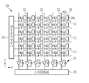
図2において、放射線画像検出装置12は、固体検出器20、波長変換層21、支持体22、縁貼り部材23、保護層24により構成されている。固体検出器20、波長変換層21、支持体22、保護層24は、放射線源11側からこの順に積層されている。放射線源11から射出され被写体15を透過した放射線は、固体検出器20を透過して波長変換層21に入射する。保護層24の放射線入射側とは反対側には、鉛板等の放射線遮蔽板(図示せず)が設けられている。
In FIG. 2, the radiation
波長変換層21は、入射した放射線を、より波長の長い光(可視光)に変換する単層の蛍光体層(シンチレータ)である。固体検出器20は、波長変換層21により変換された光を検出して放射線画像を表す画像データを生成する。縁貼り部材23は、波長変換層21及び支持体22の周縁の側面を覆っている。保護層24は、支持体22の波長変換層21とは反対側の面を覆っている。
The
また、放射線画像検出装置12は、撮影台に着脱自在に装着される電子カセッテの形態で使用されることが多い。この電子カセッテでは、放射線画像検出装置12は、筐体(図示せず)内に収納される。この筐体内に画像メモリやバッテリ(いずれも図示せず)も収納されている。筐体の放射線入射側である入射面には、放射線源11や被写体15を位置合わせするためにアライメントマーク(図示せず)が設けられている。
Further, the radiological
図3において、固体検出器20は、画素30、走査線31、データ線32、ゲートドライバ33、積分アンプ34、A/D変換器35を備える。画素30は、フォトダイオード30aとTFTスイッチ30bにより構成され、X−Y方向に2次元状に多数配列されている。走査線31は、X方向に並ぶ画素30の行毎に設けられ、TFTスイッチ30bを駆動するための走査信号が印加される。データ線32は、Y方向に並ぶ画素30の列毎に設けられ、フォトダイオード30aに蓄積され、TFTスイッチ30bを介して読み出された信号電荷が流れる。
In FIG. 3, the
フォトダイオード30aは、波長変換層21により生成された光を受けて信号電荷を発生し蓄積する。TFTスイッチ30bは、走査線31とデータ線32との各交点に対応して設けられており、フォトダイオード30aと接続されている。
The photodiode 30a receives the light generated by the
ゲートドライバ33は、各走査線31の一端に接続されており、走査線31に順に走査信号を印加する。積分アンプ34は、各データ線32の一端に接続されており、データ線32に流れる信号電荷を積算して、積算電荷に対応する電圧を出力する。A/D変換器35は、各積分アンプ34の出力側に設けられており、積分アンプ34により出力された電圧をデジタル信号に変換する。積分アンプ34とA/D変換器35との間には、電圧アンプやマルチプレクサなどが設けられるが、簡略化のため図示を省略している。A/D変換器35から出力された全画素分のデジタル信号により画像データが構成される。
The
図4において、波長変換層21は、その第1の面21aが固体検出器20に接合剤層25を介して接合されており、第2の面21bが支持体22に接合されている。接合剤層25は、アクリル系の材料により形成されている。支持体22は、樹脂フィルム22a、導電性層22b、光反射層22cがこの順に積層されたものである。この光反射層22cに波長変換層21の第2の面21bが接合されている。支持体22の下面は、保護層24で覆われている。
In FIG. 4, the
縁貼り部材23は、樹脂などから形成される。縁貼り部材23の厚さは、5μm以上500μm以下が望ましい。縁貼り部材23は、例えば、シリコーン系ポリマーとポリイソシアネートの硬化皮膜である。
The
シリコーン系ポリマーとしては、主としてポリシロキサン単位を有する成分(ポリマー、プレポリマー、またはモノマー)と、他の成分(ポリマー、プレポリマー、またはモノマー)との縮合反応あるいは重付加反応により、これらが交互、ブロックあるいはペンダントに結合したポリマーが用いられる。例えば、ポリシロキサン単位を有するポリウレタン、ポリシロキサン単位を有するポリウレア、ポリシロキサン単位を有するポリエステル、ポリシロキサン単位を有するアクリル樹脂が挙げられる。 As the silicone-based polymer, these are alternately formed by condensation reaction or polyaddition reaction of a component having a polysiloxane unit (polymer, prepolymer, or monomer) and another component (polymer, prepolymer, or monomer), Polymers attached to blocks or pendants are used. Examples thereof include polyurethane having a polysiloxane unit, polyurea having a polysiloxane unit, polyester having a polysiloxane unit, and an acrylic resin having a polysiloxane unit.
ポリイソシアネートとしては、各種ポリイソシアネート単量体、TMP(トリメチロールプロパン)等のポリオールとTDI(トリレンジイソシアネート)等(ポリ)イソシアネートの付加体、TDIの二量体あるいはTDIの三量体とHMDI(ヘキサメチレンジイソシアネート)の重合体などの重合体、ポリイソシアネートと多官能性ヒドロキシルあるいはアミン化合物又はポリイソシアネートとヒドロキシポリエーテルあるいはポリエステルとの反応により得られるイソシアネトープレポリマー等の化合物が用いられる。シリコーン系ポリマーとポリイソシアネーとの混合比は、重量比で99:1〜10:90(ポリマー:ポリイソシアネート)が一般的であり、95:5〜20:80が好ましく、さらに90:10〜70:30が好ましい。 As polyisocyanates, various polyisocyanate monomers, polyols such as TMP (trimethylolpropane) and adducts of (poly) isocyanates such as TDI (tolylene diisocyanate), dimers of TDI or trimers of TDI and HMDI A polymer such as a polymer of (hexamethylene diisocyanate), a compound such as a polyisocyanate and a polyfunctional hydroxyl or amine compound, or an isocyanate prepolymer obtained by a reaction of polyisocyanate and a hydroxy polyether or polyester is used. The mixing ratio of the silicone-based polymer and the polyisocyanate is generally 99: 1 to 10:90 (polymer: polyisocyanate) by weight, preferably 95: 5 to 20:80, and more preferably 90:10 70:30 is preferred.
支持体22の樹脂フィルム22aの材料としては、ポリエチレンテレフタレート(PET)、セルロースアセテート、ポリエステル、ポリアミド、ポリイミド、トリアセテート、ポリカーボネートなどが用いられる。樹脂フィルム22aの厚さは、20μm以上2mm以下であることが好ましく、さらに70μm以上0.5mm以下であることが好ましい。
As a material for the
導電性層22bは、ポリエステル等の樹脂にSnO2等の導電剤を分散させたものである。光反射層22cは、アクリル等の樹脂にアルミナ微粒子等の光反射性物質を分散させたものである。保護層24としては、富士フイルム株式会社製のスーパーバリアフィルム(SBF)が好適である。
The
縁貼り部材23は、導電性を含有した材料で形成してもよい。例えば、ポリマーに、SnO2:Sb、ZnOなどの導電性微粒子や、カーボンブラック、フラーレン、カーボンナノチューブ等のカーボンクラスターを混合する。この場合、縁貼り部材23のシート抵抗は108Ω以下であることが望ましい。
The
図5において、波長変換層21は、GOS(Gd2O2S:Tb)等の蛍光体粒子40を樹脂などのバインダ(結合剤)41に分散させることにより形成されている。蛍光体粒子40を球状に図示しているが、実際には、各蛍光体粒子40は、歪な多角形状である。蛍光体粒子40は、平均粒子径が5μm程度である。ここで、平均粒子径とは、例えば、フィッシャー・サブ−シーブ・サイザー(Fisher Sub-Sieve Sizer)法で測定した粒子径の平均値である。
In FIG. 5, the
蛍光体粒子40としては、A2O2S:X(ただし、Aは、Y,La,Gd,Luのうちいずれか1つ、Xは、Eu,Tb,Prのうちのいずれか1つ)で表される粒子を用いる。また、蛍光体粒子40として、A2O2S:Xに共付活剤としてセリウム(Ce)またはサマリウム(Sm)を含めたものを用いてもよく、さらに、混晶系の蛍光体を用いてもよい。
As the
波長変換層21の単位厚さ当たりの蛍光体粒子40の重量は、第1の面21a側から、放射線の入射側とは反対の第2の面21b側に向かって次第に減少している。逆に、波長変換層21の単位厚さ当たりのバインダ41の重量は、第1の面21a側から第2の面21b側に向かって次第に増大している。したがって、蛍光体粒子40の空間充填率が、固体検出器20側で大きく、固体検出器20から離れた位置で小さいため、波長変換層21は、固体検出器20側で発光量が大きく、かつ蛍光体粒子40から固体検出器20への発光の広がりが抑えられる。このため、固体検出器20により得られる画像の感度及び鮮鋭度が向上する。
The weight of the
また、波長変換層21における蛍光体粒子40の空間充填率は63%以上であることが望ましい。一般に、蛍光体の空間充填率は、以下の方法で求められる。まず、波長変換層の一部を切り出して体積を測定する。次いで、溶剤等を用いてその波長変換層から抽出した蛍光体の重量を測定し、その蛍光体の密度から蛍光体の体積を計算する。上記それぞれの体積比が蛍光体の空間充填率として表わされる。なお、蛍光体の組成が不明の場合は、組成分析を行い、構成元素と結晶構造から密度を計算すればよい。
Moreover, it is desirable that the space filling rate of the
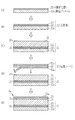
次に、放射線画像検出装置12の製造方法を説明する。まず、図6(A)に示すように、PETなどの樹脂で形成された仮支持体50を用意し、この表面にシリコーン系等の離型剤を塗布することにより離型剤層51を形成する。
Next, a method for manufacturing the radiation
図6(B)に示すように、バインダ41の溶液(結合剤溶液)に蛍光体粒子40を分散させた蛍光体塗布液を離型剤層51上にドクターブレードを用いて塗布する。蛍光体塗布液には、揮発性溶剤(MEKなど)が含まれている。離型剤層51上に塗布された蛍光体塗布液を乾燥させることにより、波長変換層21が蛍光体シートとして形成される。蛍光体塗布液を塗布した際、バインダ41の溶液内で蛍光体粒子40の比重が大きいため、蛍光体粒子40が沈降して仮支持体50側(第1の面21a側)に移動する。この移動は、乾燥によりさらに促進される。この結果、波長変換層21の単位厚さ当たりのバインダ41の重量は、仮支持体50とは反対側(第2の面21b側)から仮支持体50側(第1の面21a側)に向けて次第に小さくなる。
As shown in FIG. 6B, a phosphor coating liquid in which
図7(A)に示すように、PETなどの樹脂で形成された樹脂フィルム22aを用意し、この表面に導電性の塗布液を塗布し乾燥させ、硬化させることにより、導電性層22bを形成する。そして、図7(B)に示すように、光反射性物質を分散させた塗布液を導電性層22b上にドクターブレードを用いて塗布し、乾燥させることにより、光反射層22cが形成される。これにより、前述の支持体22が完成する。
As shown in FIG. 7A, a
続いて、図6(B)に示す工程で作成した波長変換層21を仮支持体50から剥離し、図7(C)に示すように、波長変換層21を、第2の面21bが光反射層22cに接するように、支持体22上に重ねる。そして、このように波長変換層21と支持体22とを重ねた状態で、カレンダー機を用いて加熱圧縮する。これにより、波長変換層21の第2の面21bが光反射層22cに融着する。波長変換層21の第2の面21bは、第1の面21aと比べて、バインダ41の量が多いため、加熱圧縮の際にバインダ41の溶融量が多く、光反射層22cとの密着性に優れる。
Subsequently, the
図7(D)に示すように、第1の剥離フィルム52a、接合剤層25、第2の剥離フィルム52bをこの順に積層してなる粘着シート53を用意し、この第1の剥離フィルム52aを剥離して、図7(E)に示すように、接合剤層25を波長変換層21に接合する。接合剤層25は、アクリル系の接合剤により形成されており、第1及び第2の剥離フィルム52a,52bは、PETライナーにより形成されている。
As shown in FIG. 7D, a pressure-sensitive adhesive sheet 53 is prepared by laminating a
以上の工程で作成された放射線変換シート54を規定のサイズに裁断し、図8(A)に示すように、裁断後の放射線変換シート54の周縁の側面に、ディスペンサを用いて縁貼り部材23を被覆する。このとき、縁貼り部材23は、第1の剥離フィルム52aの外周部と樹脂フィルム22aの外周部とを覆う。そして、図8(B)に示すように、樹脂フィルム22aの下面に保護層24を形成する。
The
この後、第2の剥離フィルム52bを剥離し、周知の半導体プロセスにより製造された固体検出器20の表面に、接合剤層25を介して波長変換層21の第1の面21aを接合する。具体的には、第2の剥離フィルム52bを剥離する際に、イオナイザーで接合剤層25の表面のゴミを取り除く。そして、貼り合わせ機により、放射線変換シート54と固体検出器20とを接合剤層25を介して貼り合わせ、固体検出器20の裏面からローラーで押圧することにより、固体検出器20を波長変換層21に接合させる。以上の工程で、放射線画像検出装置12が完成する。
Then, the 2nd peeling film 52b is peeled and the
放射線変換シート54の裁断時や、縁貼り部材23の形成時には、ゴミが発生する可能性があるが、これらのゴミは、第2の剥離フィルム52bに付着し、第2の剥離フィルム52bの剥離とともに除去される。また、縁貼り部材23が第1の剥離フィルム52aの外周部上にはみ出すように形成されたとしても、この部分は第1の剥離フィルム52aの剥離とともに除去されるため、固体検出器20の画素30の形成領域と波長変換層21の間に縁貼り部材23が介在することはない。
When the
波長変換層21は、バインダ41の量が少ない第1の面21aが固体検出器20に接合されるが、接合剤層25を介して接合が行われるため、密着性は確保される。
In the
次に、放射線画像撮影システム10の作用を説明する。まず、放射線源11から放射線が被写体15に向けて射出される。被写体15を透過して被写体15の放射線画像を担持した放射線が固体検出器20の側から放射線画像検出装置12に入射する。放射線画像検出装置12に入射した放射線は、固体検出器20を透過して波長変換層21に第1の面21aから入射する。波長変換層21では、入射した放射線が光(可視光)に変換される。
Next, the operation of the radiographic
ここで、波長変換層21内のバインダ41の量は、第1の面21a側が少なく、蛍光体粒子40の空間充填率が大きいため、固体検出器20の近傍で蛍光体粒子40の発光量が大きく、かつ蛍光体粒子40から固体検出器20への光の広がりが小さい。また、第1の面21a側は、バインダ41の量が少ないことにより、光が、横方向(放射線の入射方向と直交する方向)にバインダ41を介して伝播することが抑えられる。
Here, since the amount of the binder 41 in the
波長変換層21により変換された光は、固体検出器20に入射する。固体検出器20内では、光電変換が行われ、光電変換で生成された信号電荷が画素30毎に蓄積される。固体検出器20は、各画素30に蓄積された信号電荷を読み出し、1画面分の各信号電荷を画像データに変換して出力する。
The light converted by the
そして、固体検出器20から出力された画像データは、信号処理装置13に入力され、信号処理装置13において信号処理が施された後、表示装置14に入力される。表示装置14では、入力された画像データに基づいて画像表示が行われる。
The image data output from the
以下に、上述した放射線変換シート54を形成する実施例を説明する。
Below, the Example which forms the
(実施例1)
1)波長変換層の形成
ポリビニルブチラール樹脂、ウレタン樹脂脂および可塑剤の混合物20重量%を、トルエン、2−ブタノールおよびキシレンの混合溶剤80重量%に溶解し、十分に攪拌してバインダの溶液(結合剤溶液)を作成した。
Example 1
1) Formation of
この結合剤溶液と平均粒子径5μmのGd2O2S:Tb蛍光体とを固形成分として15:85の質量%比で混合し、ボールミルで分散処理して蛍光体塗布液を調製した。 This binder solution and a Gd 2 O 2 S: Tb phosphor having an average particle diameter of 5 μm were mixed as a solid component at a mass ratio of 15:85, and dispersed by a ball mill to prepare a phosphor coating solution.
この蛍光体塗布液を、ドクターブレードを用いて、シリコーン系離型剤が塗布されたPET(仮支持体、厚み:190μm)の表面に、430mmの巾で塗布し乾燥した後、仮支持体から剥離して、波長変換層(厚み:300μm)を得た。 Using a doctor blade, this phosphor coating solution was applied to the surface of PET (temporary support, thickness: 190 μm) coated with a silicone release agent in a width of 430 mm, dried, and then removed from the temporary support. It peeled and the wavelength conversion layer (thickness: 300 micrometers) was obtained.
2)導電性層の形成
下記の組成の材料にMEK(メチルエチルケトン)5gに加え、混合分散して塗布液を調製した。そして、この塗布液をPET(支持体、厚み:188μm、ヘイズ度27%、ルミラー(登録商標)S−10、東レ株式会社製)の表面にドクターブレードを用いて塗布し、乾燥させ、硬化させ、導電性層(膜厚:5μm)を形成した。
2) Formation of a conductive layer A material having the following composition was added to 5 g of MEK (methyl ethyl ketone) and mixed and dispersed to prepare a coating solution. Then, this coating solution is applied to the surface of PET (support, thickness: 188 μm, haze degree 27%, Lumirror (registered trademark) S-10, manufactured by Toray Industries, Inc.) using a doctor blade, dried and cured. A conductive layer (film thickness: 5 μm) was formed.
樹脂:飽和ポリエステル樹脂(バイロン300(登録商標)、東洋紡株式会社製)のMEK溶液(固形分30重量%)20g
硬化剤:ポリイソシアネート(オレスターNP38−70S(登録商標、三井東圧株式会社製)固形分70%)2g
導電剤:SnO2(Sbドープ)針状微粒子のMEK分散体(固形分30重量%)50g
Resin: MEK solution (
Curing agent: Polyisocyanate (Olestar NP38-70S (registered trademark, manufactured by Mitsui Toatsu Co., Ltd.)
Conductive agent: SnO 2 (Sb dope) needle-shaped fine particle MEK dispersion (
3)光反射層の形成
続いて、下記組成の材料をMEK387gに加え、混合分散して塗布液を作製した。この塗布液を導電性層の表面にドクターブレードを用いて塗布し乾燥して、光反射層(層厚、約100μm)を形成した。
3) Formation of light reflecting layer Subsequently, a material having the following composition was added to 387 g of MEK and mixed and dispersed to prepare a coating solution. This coating solution was applied to the surface of the conductive layer using a doctor blade and dried to form a light reflecting layer (layer thickness, about 100 μm).
光反射性物質:高純度アルミナ微粒子(平均粒子経:0.4μm)444g
結合剤:軟質アクリル樹脂(クリスコートP−1018GS(登録商標、大日本インキ化学工業株式会社製)「20%トルエン溶液」)100g
Light reflecting material: high purity alumina fine particles (average particle size: 0.4 μm) 444 g
Binder: Soft acrylic resin (Chriscoat P-1018GS (registered trademark, manufactured by Dainippon Ink & Chemicals, Inc.) “20% toluene solution”) 100 g
4)波長変換層と光反射層との接合
光反射層の面上に、1)で作製した波長変換層を塗布形成時の上面(仮支持体とは反対側)が接するようにして重ね、カレンダー機を用いて総荷重2300kg、上側ロール45℃、下側ロール45℃、送り速度0.3m/分にて加熱圧縮した。これにより、波長変換層は光反射層に完全に融着した。熱圧縮後の層厚は200μmであった。
4) Bonding of wavelength conversion layer and light reflection layer Overlaid on the surface of the light reflection layer so that the wavelength conversion layer prepared in 1) is in contact with the upper surface (on the side opposite to the temporary support) at the time of coating, The calender machine was used for heat compression with a total load of 2300 kg, an upper roll of 45 ° C., a lower roll of 45 ° C., and a feed rate of 0.3 m / min. Thereby, the wavelength conversion layer was completely fused to the light reflection layer. The layer thickness after heat compression was 200 μm.
5)接合剤層および剥離フィルムの形成
粘着シートとして、PETライナー38μm(軽剥離)/アクリル系接合剤層15μm/PETライナー75μm(重剥離)の構成のものを用い、軽剥離側の剥離フィルムを剥離し、接合剤層を蛍光体層と接合した。
5) Formation of bonding agent layer and release film As the pressure-sensitive adhesive sheet, use a PET liner having a configuration of 38 μm (light release) /
6)縁貼り部材の形成
1)〜5)で作製した放射線変換シートを規定のサイズに裁断した後、縁貼り部材のディスペンサにセットし、ロボットを制御して蛍光体層の周縁の側面を縁貼り部材で被覆した。縁貼り部材としては、下記組成の混合物をメチルエチルケトン150gに溶解させて調製した被覆液を使用した。
6) Formation of edge pasting member After cutting the radiation conversion sheet prepared in 1) to 5) to a specified size, set it to the dispenser of the edge pasting member, and control the robot to border the peripheral side surface of the phosphor layer. It covered with the pasting member. As the edge pasting member, a coating solution prepared by dissolving a mixture having the following composition in 150 g of methyl ethyl ketone was used.
シリコーン系ポリマー:ポリジメチルシロキサン単位を有するポリウレタン(大日精化(株)、ダイアロマ−SP3023[15%メチルエチルケトン溶液])700g
架橋剤:ポリイソシアネート(大日精化(株)、クロスネートD−70[50%溶液])30g
黄変防止剤:エポキシ樹脂(油化シェルエポキシ(株)、エピ コート#1001[固形])6g
滑り剤:アルコール変成シリコーン(信越化学(株)、X−2 2−2809[66%キシレン含有ペースト])2g
Silicone polymer: Polyurethane having a polydimethylsiloxane unit (Daiichi Seika Co., Ltd., Dialoma-SP3023 [15% methyl ethyl ketone solution]) 700 g
Crosslinking agent: 30 g of polyisocyanate (Daiichi Seika Co., Ltd., Crossnate D-70 [50% solution])
Yellowing prevention agent: Epoxy resin (Oilized Shell Epoxy Co., Ltd., Epicoat # 1001 [solid]) 6 g
Sliding agent: Alcohol-modified silicone (Shin-Etsu Chemical Co., Ltd., X-2 2-2809 [66% xylene-containing paste]) 2 g
そして、得られた被覆液を、コロナ放電処理済の放射線変換シートの端部全周(端部から1mm内側までを含む)に塗布し、室温で充分に乾燥して、膜厚約25μmの端部皮膜を形成した。 Then, the obtained coating liquid is applied to the entire circumference of the end portion of the radiation conversion sheet that has been subjected to the corona discharge treatment (including from the end portion to the inside of 1 mm), and is sufficiently dried at room temperature to obtain an end having a film thickness of about 25 μm. A partial film was formed.
(第2実施形態)
第1実施形態では、ほぼ一定の大きさの蛍光体粒子40をバインダ41に分散させて波長変換層21を形成しているが、第2実施形態として、図9に示すように、大きさの異なる第1及び第2の蛍光体粒子61,62をバインダ63内に混合させて波長変換層60を形成してもよい。第2実施形態の放射線画像検出装置は、波長変換層21に代えて波長変換層60を用いること以外は、第1実施形態の放射線画像検出装置12と同一構成である。
(Second Embodiment)
In the first embodiment, the
第1の蛍光体粒子61の平均粒子径D1は、第2の蛍光体粒子62の平均粒子径D2より大きい。第1の蛍光体粒子61の平均粒子径D1は、5μm以上12μm以下であることが好ましく、6μm程度であることがより好ましい。第2の蛍光体粒子62の平均粒子径D2は、1μm以上5μm未満であることが好ましく、2μm程度であることがより好ましい。本実施形態では、平均粒子径が大きい第1の蛍光体粒子61の隙間に、平均粒子径が小さい第2の蛍光体粒子62が入り込むため、蛍光体の空間充填率が向上し、画質が向上する。
The average particle diameter D1 of the
第1の蛍光体粒子61と第2の蛍光体粒子62とは、両者とも同じ材料(例えば、GOS)で形成されたものでもよいし、それぞれ異なる材料(例えば、GOSとLOS(Lu2O2S:Tb))で形成されたものでもよい。
Both the
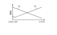
波長変換層60内において第1の蛍光体粒子61と第2の蛍光体粒子62とを合わせた空間充填率SFRは、第1の蛍光体粒子61に対する第2の蛍光体粒子62の重量比WRに依存する。図10において、実線は、D1=6μm、D2=2μmとした場合の空間充填率SFRであり、重量比WRが約30%のときに空間充填率SFRが最大となることを示している。この場合、重量比WRは、20%〜40%の範囲内であることが好ましく、この範囲で、空間充填率SFRは約68%以上となる。
The space filling ratio SFR of the
これに対して、一点鎖線は、D1=10μm、D2=2μmとした場合の空間充填率SFRであり、二点差線は、D1=4μm、D2=2μmとした場合の空間充填率SFRである。このように、第1の蛍光体粒子61の平均粒子径D1を大きくするほど、第1の蛍光体粒子61間の隙間に第2の蛍光体粒子62が入りやすくなり、空間充填率SFRが向上する。
On the other hand, the one-dot chain line is the space filling rate SFR when D1 = 10 μm and D2 = 2 μm, and the two-dotted line is the space filling rate SFR when D1 = 4 μm and D2 = 2 μm. Thus, as the average particle diameter D1 of the
図11において、波長変換層60の単位厚さ当たりの第1の蛍光体粒子61の重量W1は、固体検出器20側から支持体22側に向かって次第に減少している。逆に、波長変換層60の単位厚さ当たりの第2の蛍光体粒子62の重量W2は、固体検出器20側から支持体22側に向かって次第に増大している。このように、平均粒子径の大きな第1の蛍光体粒子61は固体検出器20側に多く存在し、平均粒子径の小さな第2の蛍光体粒子62は支持体22側に多く存在するため、高感度で高鮮鋭度の画像が得られる。なお、図11では、重量の分布を模式的に直線で表しているが、実際は曲線である。
In FIG. 11, the weight W1 of the
波長変換層60を製造するには、第1の蛍光体粒子61と第2の蛍光体粒子62とをバインダ63の溶液に分散させた蛍光体塗布液を、仮支持体上に塗布して乾燥させればよい。こうすることで、平均粒子径が大きい第1の蛍光体粒子61は、沈降して仮支持体側に移動する。一方の平均粒子径が小さい第2の蛍光体粒子62は、仮支持体側の大部分が第1の蛍光体粒子61により占有されるため、第1の蛍光体粒子61の間の隙間に入り込む分以外は、仮支持体とは反対側に移動する。これにより、前述の重量の分布が得られる。波長変換層60の単位厚さ当たりのバインダ63の重量は、第1実施形態と同様に、仮支持体とは反対側から仮支持体側に向かって次第に減少する。
In order to manufacture the
上記の蛍光体塗布液の乾燥条件を制御することで、第1の蛍光体粒子61の仮支持体側への移動量を調整することができる。例えば、蛍光体塗布液を、時間を掛けてゆっくり乾燥させた場合には、第1の蛍光体粒子61の仮支持体側への移動量が大きく、仮支持体側における第1の蛍光体粒子61の空間充填率がより高まる。
The amount of movement of the
また、蛍光体塗布液の塗布時の温度をやや上昇(例えば、通常の温度が25℃であれば、25℃や30℃に上昇)させることで、蛍光体塗布液の粘度が低下し、第1の蛍光体粒子61が移動しやすくなる。このように、蛍光体塗布液の塗布時の温度を制御することで、第1の蛍光体粒子61の仮支持体側への移動量を調整することができる。
Further, by slightly increasing the temperature at the time of applying the phosphor coating solution (for example, if the normal temperature is 25 ° C., it is increased to 25 ° C. or 30 ° C.), the viscosity of the phosphor coating solution is decreased, One
このように形成された波長変換層60は、図12に示すように、仮支持体側の表面60aには、接合剤層25を介して固体検出器20に接合され、仮支持体と反対側の表面60bには、光反射層22cが接合される。
As shown in FIG. 12, the
また、重量比WRの値によっては、図13及び図14に示すように、第2の蛍光体粒子62の重量W2が、固体検出器20側付近で、固体検出器20側から支持体22側に向かって単調に増大しない場合がある。これは、蛍光体塗布液の乾燥の際に、第2の蛍光体粒子62の塗布表面方向への上昇が、第1の蛍光体粒子61により阻止されることによる。一方の第1の蛍光体粒子61は、第2の蛍光体粒子62より粒子径が大きいため、第2の蛍光体粒子62よる阻止は殆ど生じず、固体検出器20側から支持体22側に向かって単調に減少する。図13は、重量W2が、固体検出器20側から支持体22側に向かって減少した後、単調に増大する場合を示している。図14は、重量W2が、固体検出器20側から支持体22側に向かって増大して減少した後、単調に増大する場合を示している。
Further, depending on the value of the weight ratio WR, as shown in FIGS. 13 and 14, the weight W2 of the
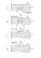
本実施形態では、蛍光体塗布液を仮支持体上に塗布して乾燥した際に、その塗布表面(波長変換層60の表面60b)には、泡脹れ(ブリスタ)と呼ばれる凸部が生じる恐れがある。これは、蛍光体塗布液の乾燥中に、塗布表面である表面60b側から乾燥が進行し、図15(A)に示すように、蛍光体塗布液が乾燥することにより形成されるバインダ63内に、揮発性溶剤が揮発せずに残留した複数の残留溶剤63aが生じるためである。これらの残留溶剤63aは、乾燥が進むに連れて、図15(B)に示すように凝集して凝集体63bとなり、この凝集体63bは、バインダ63内から抜け出ようとして表面60bを隆起させる。この隆起が進行することにより、図15(C)に示すように、凝集体63bと表面60bとの間にクラック60cが生じ、このクラック60cを通じて凝集体63b内の揮発した溶剤が放出される。この結果、図15(D)に示すように、表面60bには、カルデラ状のブリスタが生じ、凸部60dが形成される。
In the present embodiment, when the phosphor coating liquid is coated on a temporary support and dried, a convex portion called a blister is generated on the coating surface (the
カルデラ状の凸部60dの直径は、数mm〜1cm程度である。凸部60dの表面60bからの突出量は、100〜200μm程度である。これに対して、波長変換層60の厚みは、300μm程度である。
The diameter of the caldera-like
このブリスタは、表面60b付近における第1の蛍光体粒子61の平均粒子径D1が大きい程生じやすいという傾向にある。これは、乾燥による揮発性溶剤の表面60b側への上昇が、粒子径が大きな第1の蛍光体粒子61により阻止されて残留するためである。本実施形態では、蛍光体塗布液の乾燥時間を長くし、バインダ63を蛍光体塗布液の塗布表面側に多く移動させることにより、表面60b側における第1の蛍光体粒子61の量を少なくしているため、ブリスタの発生は低減される。このブリスタによる凸部60dは、図12に示すように、波長変換層60の表面60bと光反射層22cとの間に、空気層65を生じさせる。しかし、この空気層65は、屈折率が波長変換層60より低いため、波長変換層60と光反射層22cとの間における光の反射率を高め、高感度化に寄与する。
This blister tends to occur more easily as the average particle diameter D1 of the
このように、本実施形態では、表面60bの凸部60dは、感度特性に有利な方向に働くため、平均粒子径D1が大きな第1の蛍光体粒子61を用いることができる。例えば、図10に示すように、最大75%の空間充填率SFRが得られる平均粒子径D1が10μmの第1の蛍光体粒子61を用いることができ、さらに感度化が向上する。
Thus, in this embodiment, since the
一方の波長変換層60の表面60aは、ブリスタが生じないため、接合剤層25の密着性が高い。また、表面60aと接合剤層25との間には、空気層が殆ど生じないため、光の反射や散乱が生じにくい。この点も、高感度化及び高鮮鋭度化に有利である。
Since the blister is not generated on the
また、本実施形態では、波長変換層60の表面60a側から放射線が入射され、波長変換層60内での主発光領域が表面60a側であるので、発光が上記のブリスタに影響されることはなく、高鮮鋭度化に有利である。
Further, in the present embodiment, radiation is incident from the
波長変換層が大きさの異なる2種の蛍光体粒子が分散された2粒子系であるか否かは、前述のフィッシャー・サブ−シーブ・サイザー法により検出可能である。波長変換層が2粒子系であり、2種の蛍光体粒子の平均粒子径の差が大きい(D1=6μm、D2=2μm)であれば、図16に示すように、平均粒子径の度数分布に明確な2つのピークが現れる。 Whether or not the wavelength conversion layer is a two-particle system in which two types of phosphor particles having different sizes are dispersed can be detected by the above-described Fischer sub-sieve sizer method. If the wavelength conversion layer is a two-particle system and the difference in average particle size between the two types of phosphor particles is large (D1 = 6 μm, D2 = 2 μm), as shown in FIG. 16, the frequency distribution of the average particle size Two clear peaks appear.
(第3実施形態)
第2実施形態では、大きさの異なる2種の蛍光体粒子をバインダ内に混合させて波長変換層を形成しているが、さらに、大きさの異なる3種の蛍光体粒子をバインダ内に混合させて波長変換層を形成してもよい。この場合、小さな蛍光体粒子が他の蛍光体粒子間の隙間に入り込むため、蛍光体の空間充填率がより向上し、画質がより向上する。
(Third embodiment)
In the second embodiment, two types of phosphor particles having different sizes are mixed in the binder to form the wavelength conversion layer, but three types of phosphor particles having different sizes are further mixed in the binder. A wavelength conversion layer may be formed. In this case, since the small phosphor particles enter the gaps between the other phosphor particles, the space filling rate of the phosphor is further improved, and the image quality is further improved.
第3実施形態として、図17に示す波長変換層70を適用する。波長変換層70は、大きさの異なる第1の蛍光体粒子71、第2の蛍光体粒子72、第3の蛍光体粒子73をバインダ74に分散させたものである。第1の蛍光体粒子71の平均粒子径は、9μm以上12μm以下であることが好ましく、10μm程度であることがより好ましい。第2の蛍光体粒子72の平均粒子径は、1μm以上5μm未満であることが好ましく、2μm程度であることがより好ましい。第3の蛍光体粒子73の平均粒子径は、5μm以上9μm未満であることが好ましく、6μm程度であることがより好ましい。
As the third embodiment, a
第1の蛍光体粒子71、第2の蛍光体粒子72、第3の蛍光体粒子73は、同じ材料で形成されたものでもよいし、それぞれ異なる材料で形成されたものでもよい。第1の蛍光体粒子71、第2の蛍光体粒子72、第3の蛍光体粒子73の重量比は、約5:2:3であることが好ましい。波長変換層70内の第1〜3の蛍光体粒子71〜73を合わせた空間充填率は、68%以上であることが好ましい。
The
図18において、波長変換層70の単位厚さ当たりの第1の蛍光体粒子71の重量W1は、固体検出器20側から支持体22側に向かって次第に減少している。逆に、波長変換層70の単位厚さ当たりの第2の蛍光体粒子72の重量W2は、固体検出器20側から支持体22側に向かって次第に増大している。そして、波長変換層70の単位厚さ当たりの第3の蛍光体粒子73の重量W3は、厚さ方向にあまり変化がない。
In FIG. 18, the weight W1 of the
このように、固体検出器20側では、第2の蛍光体粒子72、第3の蛍光体粒子73、第1の蛍光体粒子71の順に空間充填率が高くなり、支持体22側では、第1の蛍光体粒子71、第3の蛍光体粒子73、第2の蛍光体粒子72の順に空間充填率が高くなる。平均粒子径の大きな第1の蛍光体粒子71が固体検出器20側に多く存在し、平均粒子径の小さな第2の蛍光体粒子72が支持体22側に多く存在するため、高感度で高鮮鋭度の画像が得られる。また、第1〜3の蛍光体粒子71〜73の平均粒子径に依存して、固体検出器20側における第2の蛍光体粒子72の重量W2と第3の蛍光体粒子73の重量W3との関係が逆になる可能性もある。また、本実施形態においても第2の蛍光体粒子72の重量W2は、固体検出器20側付近で、固体検出器20側から支持体22側に向かって単調に増大しない場合がある。
Thus, on the
波長変換層70を製造するには、第2実施形態と同様に、第1の蛍光体粒子71、第2の蛍光体粒子72、第3の蛍光体粒子73をそれぞれバインダ74の溶液に分散させた蛍光体塗布液を、仮支持体上に塗布し乾燥させればよい。このようにして形成された波長変換層70の仮支持体側の面が固体検出器20に接合される。本実施形態のその他の構成は、第2実施形態と同一である。
In order to manufacture the
前述のように、本実施形態においても、蛍光体塗布液の乾燥により、塗布表面にブリスタが発生するが、本実施形態では、平均粒子径が大きな第1の蛍光体粒子71の量を蛍光体塗布液の塗布表面側で少なくしているため、ブリスタの発生が低減される。このため、例えば、平均粒子径が10μmの大きな第1の蛍光体粒子71を用いることができる。本実施形態のその他の効果は、第2実施形態と同様である。
As described above, also in the present embodiment, blisters are generated on the coating surface due to the drying of the phosphor coating solution. In this embodiment, the amount of the
さらに、バインダに平均粒子径の異なる4種以上の蛍光体粒子を分散させることにより波長変換層を形成してもよい。 Further, the wavelength conversion layer may be formed by dispersing four or more kinds of phosphor particles having different average particle diameters in the binder.
(その他の実施形態)
上記各実施形態では、仮支持体に蛍光体塗布液を塗布し、平均粒子径の大きな蛍光体粒子を、その自重により仮支持体側に移動させることにより、仮支持体側の重量(空間充填率)を高めているが、これに代えて、蛍光体粒子の表面に界面活性剤を付着させ、界面活性剤で得られる浮力により、蛍光体粒子を仮支持体とは反対側に移動させてもよい。大きさの異なる複数の蛍光体粒子に界面活性剤を付着させ、これらをバインダに分散させた場合には、平均粒子径が大きな蛍光体粒子ほど大きな浮力が得られるため、仮支持体とは反対側に移動しやすくなる。この場合には、形成された波長変換層の仮支持体とは反対側を固体検出器20に接合すればよい。
(Other embodiments)
In each of the above embodiments, the weight of the temporary support (the space filling factor) is obtained by applying the phosphor coating liquid to the temporary support and moving the phosphor particles having a large average particle diameter to the temporary support by its own weight. Alternatively, a surfactant may be attached to the surface of the phosphor particles, and the phosphor particles may be moved to the opposite side of the temporary support by buoyancy obtained with the surfactant. . When a surfactant is attached to a plurality of phosphor particles of different sizes and these are dispersed in a binder, the larger the average particle diameter, the greater the buoyancy that can be obtained. Easy to move to the side. In this case, what is necessary is just to join the solid
上記各実施形態では、波長変換層を、接合剤層を介して固体検出器に接合しているが、波長変換層が固体検出器に直接接するように押し当てた状態としてもよい。 In each of the embodiments described above, the wavelength conversion layer is bonded to the solid state detector via the bonding agent layer. However, the wavelength conversion layer may be pressed so as to be in direct contact with the solid state detector.
10 放射線画像撮影システム
12 放射線画像検出装置
20 固体検出器
21 波長変換層
22 支持体
22c 光反射層
23 縁貼り部材
25 接合剤層
40 蛍光体粒子
41 バインダ
60 波長変換層
61 第1の蛍光体粒子
62 第2の蛍光体粒子
63 バインダ
70 波長変換層
71 第1の蛍光体粒子
72 第2の蛍光体粒子
73 第3の蛍光体粒子
74 バインダ
DESCRIPTION OF
Claims (14)
前記波長変換層は、少なくとも、第1の平均粒子径を有する第1の蛍光体粒子と、前記第1の平均粒子径より小さい第2の平均粒子径を有する第2の蛍光体粒子とをバインダ中に混合した単層の蛍光体層であり、前記波長変換層の単位厚さ当たりの前記第1の蛍光体粒子の重量は、前記固体検出器から離れる方向に向かって次第に減少していることを特徴とする放射線画像検出装置。 A wavelength conversion layer that converts radiation into light; and a solid-state detector that detects the light and generates image data. The solid-state detector and the wavelength conversion layer from the side on which radiation enters from a radiation source during imaging In the radiation image detection apparatus arranged in the order of
The wavelength conversion layer includes at least a first phosphor particle having a first average particle diameter and a second phosphor particle having a second average particle diameter smaller than the first average particle diameter. A single-layer phosphor layer mixed therein, and the weight of the first phosphor particles per unit thickness of the wavelength conversion layer gradually decreases in a direction away from the solid state detector. A radiological image detection apparatus characterized by the above.
前記放射線を光に変換する波長変換層と、前記光を検出して画像データを生成する固体検出器とを有する放射線画像検出装置であり、前記放射線が入射する側から順に、前記固体検出器、前記波長変換層の順に配置されており、前記波長変換層は、少なくとも、第1の平均粒子径を有する第1の蛍光体粒子と、前記第1の平均粒子径より小さい第2の平均粒子径を有する第2の蛍光体粒子とをバインダ中に混合した単層の蛍光体層であり、前記波長変換層の単位厚さ当たりの前記第1の蛍光体粒子の重量は、前記固体検出器から離れる方向に向かって次第に減少している放射線画像検出装置と、
を備えることを特徴とする放射線画像撮影システム。 A radiation source that emits radiation;
A radiation image detection device having a wavelength conversion layer that converts the radiation into light and a solid state detector that detects the light and generates image data, and in order from the side on which the radiation is incident, the solid state detector, The wavelength conversion layers are arranged in the order, and the wavelength conversion layer includes at least a first phosphor particle having a first average particle diameter and a second average particle diameter smaller than the first average particle diameter. A single-layer phosphor layer in which a binder is mixed with a second phosphor particle having a weight, and the weight of the first phosphor particle per unit thickness of the wavelength conversion layer is determined from the solid-state detector. A radiological image detection apparatus that gradually decreases in the direction of separation;
A radiographic imaging system comprising:
Priority Applications (4)
| Application Number | Priority Date | Filing Date | Title |
|---|---|---|---|
| JP2013045386A JP5744941B2 (en) | 2012-03-12 | 2013-03-07 | Radiographic image detection apparatus and radiographic imaging system |
| CN201380006771.5A CN104081224B (en) | 2012-03-12 | 2013-03-08 | Radiological image detection and radiation image picking-up system |
| PCT/JP2013/056447 WO2013137138A1 (en) | 2012-03-12 | 2013-03-08 | Radiation image detecting device and radiation image pickup system |
| US14/335,260 US9052401B2 (en) | 2012-03-12 | 2014-07-18 | Radiation image detection device and radiation imaging system |
Applications Claiming Priority (3)
| Application Number | Priority Date | Filing Date | Title |
|---|---|---|---|
| JP2012054507 | 2012-03-12 | ||
| JP2012054507 | 2012-03-12 | ||
| JP2013045386A JP5744941B2 (en) | 2012-03-12 | 2013-03-07 | Radiographic image detection apparatus and radiographic imaging system |
Publications (3)
| Publication Number | Publication Date |
|---|---|
| JP2013217913A JP2013217913A (en) | 2013-10-24 |
| JP2013217913A5 JP2013217913A5 (en) | 2014-08-21 |
| JP5744941B2 true JP5744941B2 (en) | 2015-07-08 |
Family
ID=49161048
Family Applications (1)
| Application Number | Title | Priority Date | Filing Date |
|---|---|---|---|
| JP2013045386A Active JP5744941B2 (en) | 2012-03-12 | 2013-03-07 | Radiographic image detection apparatus and radiographic imaging system |
Country Status (4)
| Country | Link |
|---|---|
| US (1) | US9052401B2 (en) |
| JP (1) | JP5744941B2 (en) |
| CN (1) | CN104081224B (en) |
| WO (1) | WO2013137138A1 (en) |
Families Citing this family (8)
| Publication number | Priority date | Publication date | Assignee | Title |
|---|---|---|---|---|
| JP6226579B2 (en) * | 2013-06-13 | 2017-11-08 | 東芝電子管デバイス株式会社 | Radiation detector and manufacturing method thereof |
| JP6326006B2 (en) * | 2014-06-20 | 2018-05-16 | 富士フイルム株式会社 | Transfer material, method for manufacturing liquid crystal panel, and method for manufacturing liquid crystal display device |
| JP6575105B2 (en) | 2015-03-27 | 2019-09-18 | コニカミノルタ株式会社 | Scintillator panel and manufacturing method thereof |
| WO2017188191A1 (en) * | 2016-04-25 | 2017-11-02 | 日本特殊陶業株式会社 | Wavelength conversion member, production method therefor, and light emitting device |
| JP2018189425A (en) * | 2017-04-28 | 2018-11-29 | 三菱ケミカル株式会社 | X-ray image conversion screen, x-ray imaging device, and x-ray inspection device |
| JP2019023579A (en) * | 2017-07-24 | 2019-02-14 | コニカミノルタ株式会社 | Scintillator |
| CN111819707B (en) * | 2018-03-08 | 2023-05-02 | 夏普株式会社 | Element, electronic device, and method for manufacturing element |
| JP7333244B2 (en) * | 2019-10-24 | 2023-08-24 | 浜松ホトニクス株式会社 | RADIATION DETECTOR AND METHOD FOR MANUFACTURING RADIATION DETECTOR |
Family Cites Families (14)
| Publication number | Priority date | Publication date | Assignee | Title |
|---|---|---|---|---|
| JPH0664196B2 (en) * | 1986-03-14 | 1994-08-22 | コニカ株式会社 | Radiation image conversion panel |
| JP3913342B2 (en) * | 1997-12-18 | 2007-05-09 | 株式会社東芝 | Radiation intensifying screen and radiation inspection equipment using it |
| JP3838849B2 (en) * | 2000-03-28 | 2006-10-25 | 株式会社東芝 | X-ray flat panel detector |
| US7053380B2 (en) * | 2002-02-08 | 2006-05-30 | Kabushiki Kaisha Toshiba | X-ray detector and method for producing X-ray detector |
| WO2004095068A1 (en) * | 2003-04-24 | 2004-11-04 | Philips Intellectual Property & Standards Gmbh | Detector element for spatially resolved detection of gamma radiation |
| DE50309075D1 (en) * | 2003-07-02 | 2008-03-13 | Agfa Gevaert Healthcare Gmbh | System with a scanner and a storage layer and storage layer for storing x-ray information |
| JP2005106682A (en) * | 2003-09-30 | 2005-04-21 | Konica Minolta Medical & Graphic Inc | Radiation image conversion panel and its manufacturing method |
| US7304309B2 (en) * | 2005-03-14 | 2007-12-04 | Avraham Suhami | Radiation detectors |
| JP4134993B2 (en) * | 2005-03-24 | 2008-08-20 | 日立金属株式会社 | X-ray detector |
| JP4095648B2 (en) * | 2006-11-06 | 2008-06-04 | 株式会社東芝 | Production method of radiation intensifying screen |
| JP5313632B2 (en) * | 2008-11-04 | 2013-10-09 | 富士フイルム株式会社 | Radiation image detector |
| JP2010121997A (en) * | 2008-11-18 | 2010-06-03 | Fujifilm Corp | Radiation image detector |
| JP2012026932A (en) * | 2010-07-26 | 2012-02-09 | Fujifilm Corp | Radiation detector |
| JP5340444B2 (en) * | 2012-03-12 | 2013-11-13 | 富士フイルム株式会社 | Radiographic image detection apparatus and radiographic imaging system |
-
2013
- 2013-03-07 JP JP2013045386A patent/JP5744941B2/en active Active
- 2013-03-08 CN CN201380006771.5A patent/CN104081224B/en active Active
- 2013-03-08 WO PCT/JP2013/056447 patent/WO2013137138A1/en active Application Filing
-
2014
- 2014-07-18 US US14/335,260 patent/US9052401B2/en active Active
Also Published As
| Publication number | Publication date |
|---|---|
| CN104081224A (en) | 2014-10-01 |
| WO2013137138A1 (en) | 2013-09-19 |
| JP2013217913A (en) | 2013-10-24 |
| US20150010130A1 (en) | 2015-01-08 |
| CN104081224B (en) | 2016-02-03 |
| US9052401B2 (en) | 2015-06-09 |
Similar Documents
| Publication | Publication Date | Title |
|---|---|---|
| JP5744941B2 (en) | Radiographic image detection apparatus and radiographic imaging system | |
| JP5340444B2 (en) | Radiographic image detection apparatus and radiographic imaging system | |
| JP5791281B2 (en) | Radiation detection apparatus and radiation detection system | |
| JP5785201B2 (en) | Radiation image detection device | |
| US8399842B2 (en) | Digital radiographic detector with bonded phosphor layer | |
| JP5313632B2 (en) | Radiation image detector | |
| US8647965B2 (en) | Radiographic image detector, method of producing the same, and protective member | |
| JP5702047B2 (en) | Radiation conversion sheet and radiation image detector | |
| JPWO2016167334A1 (en) | Radiation image conversion screen, flat panel detector, radiation detector, and scintillator | |
| JP5102398B2 (en) | Radiation image detector | |
| JP2010096616A (en) | Radiographic image detector | |
| JP2010121997A (en) | Radiation image detector | |
| JP2010025780A (en) | Radiation conversion sheet and radiological image detection apparatus | |
| JP2019060821A (en) | Panel for x-ray talbot imaging | |
| KR20170113264A (en) | Radiation detection apparatus and radiation imaging system | |
| JP2015222261A (en) | Radiation image detection device | |
| JP4307127B2 (en) | Radiography equipment | |
| JP2010107198A (en) | Radiation image detector | |
| EP3940429B1 (en) | Radiation imaging panel, radiation imaging apparatus, radiation imaging system, and scintillator plate | |
| JP2022039047A (en) | Radiographic imaging panel, radiographic imaging device, radiographic imaging system, and scintillator plate | |
| KR20210081146A (en) | Curved Radiation Detector for Implementing Low Dose and High Resolution using Backside Light-Receiving Structure | |
| JP2017049100A (en) | Radiation detection device, radiation detect system and manufacturing method for radiation detection device |
Legal Events
| Date | Code | Title | Description |
|---|---|---|---|
| A621 | Written request for application examination |
Free format text: JAPANESE INTERMEDIATE CODE: A621 Effective date: 20140613 |
|
| A521 | Request for written amendment filed |
Free format text: JAPANESE INTERMEDIATE CODE: A523 Effective date: 20140708 |
|
| TRDD | Decision of grant or rejection written | ||
| A01 | Written decision to grant a patent or to grant a registration (utility model) |
Free format text: JAPANESE INTERMEDIATE CODE: A01 Effective date: 20150401 |
|
| A61 | First payment of annual fees (during grant procedure) |
Free format text: JAPANESE INTERMEDIATE CODE: A61 Effective date: 20150430 |
|
| R150 | Certificate of patent or registration of utility model |
Ref document number: 5744941 Country of ref document: JP Free format text: JAPANESE INTERMEDIATE CODE: R150 |
|
| R250 | Receipt of annual fees |
Free format text: JAPANESE INTERMEDIATE CODE: R250 |
|
| R250 | Receipt of annual fees |
Free format text: JAPANESE INTERMEDIATE CODE: R250 |
|
| R250 | Receipt of annual fees |
Free format text: JAPANESE INTERMEDIATE CODE: R250 |
|
| R250 | Receipt of annual fees |
Free format text: JAPANESE INTERMEDIATE CODE: R250 |
|
| R250 | Receipt of annual fees |
Free format text: JAPANESE INTERMEDIATE CODE: R250 |
|
| R250 | Receipt of annual fees |
Free format text: JAPANESE INTERMEDIATE CODE: R250 |
|
| R250 | Receipt of annual fees |
Free format text: JAPANESE INTERMEDIATE CODE: R250 |