JP5740901B2 - Light emitting device and display device - Google Patents
Light emitting device and display device Download PDFInfo
- Publication number
- JP5740901B2 JP5740901B2 JP2010232752A JP2010232752A JP5740901B2 JP 5740901 B2 JP5740901 B2 JP 5740901B2 JP 2010232752 A JP2010232752 A JP 2010232752A JP 2010232752 A JP2010232752 A JP 2010232752A JP 5740901 B2 JP5740901 B2 JP 5740901B2
- Authority
- JP
- Japan
- Prior art keywords
- light emitting
- emitting elements
- column
- emitting element
- light
- Prior art date
- Legal status (The legal status is an assumption and is not a legal conclusion. Google has not performed a legal analysis and makes no representation as to the accuracy of the status listed.)
- Expired - Fee Related
Links
- 239000013078 crystal Substances 0.000 claims description 214
- 239000000758 substrate Substances 0.000 claims description 190
- 239000011159 matrix material Substances 0.000 claims description 39
- 239000004065 semiconductor Substances 0.000 claims description 18
- 230000010287 polarization Effects 0.000 claims description 10
- 239000010410 layer Substances 0.000 description 75
- 238000000034 method Methods 0.000 description 35
- 238000010586 diagram Methods 0.000 description 34
- 239000003086 colorant Substances 0.000 description 25
- 238000005286 illumination Methods 0.000 description 22
- 239000012790 adhesive layer Substances 0.000 description 19
- 230000004048 modification Effects 0.000 description 17
- 238000012986 modification Methods 0.000 description 17
- 238000009826 distribution Methods 0.000 description 14
- 239000000463 material Substances 0.000 description 12
- 238000004519 manufacturing process Methods 0.000 description 9
- 230000003287 optical effect Effects 0.000 description 8
- 229910052594 sapphire Inorganic materials 0.000 description 7
- 239000010980 sapphire Substances 0.000 description 7
- 239000010453 quartz Substances 0.000 description 5
- VYPSYNLAJGMNEJ-UHFFFAOYSA-N silicon dioxide Inorganic materials O=[Si]=O VYPSYNLAJGMNEJ-UHFFFAOYSA-N 0.000 description 5
- 230000000694 effects Effects 0.000 description 4
- 239000011521 glass Substances 0.000 description 4
- 239000011347 resin Substances 0.000 description 4
- 229920005989 resin Polymers 0.000 description 4
- 230000005855 radiation Effects 0.000 description 3
- 229910001218 Gallium arsenide Inorganic materials 0.000 description 2
- 150000001875 compounds Chemical class 0.000 description 2
- 239000004020 conductor Substances 0.000 description 2
- 239000010949 copper Substances 0.000 description 2
- 238000001312 dry etching Methods 0.000 description 2
- 239000010931 gold Substances 0.000 description 2
- 239000000203 mixture Substances 0.000 description 2
- 150000004767 nitrides Chemical class 0.000 description 2
- 238000001039 wet etching Methods 0.000 description 2
- 229910018072 Al 2 O 3 Inorganic materials 0.000 description 1
- RYGMFSIKBFXOCR-UHFFFAOYSA-N Copper Chemical compound [Cu] RYGMFSIKBFXOCR-UHFFFAOYSA-N 0.000 description 1
- JMASRVWKEDWRBT-UHFFFAOYSA-N Gallium nitride Chemical compound [Ga]#N JMASRVWKEDWRBT-UHFFFAOYSA-N 0.000 description 1
- 229910004541 SiN Inorganic materials 0.000 description 1
- 229910004298 SiO 2 Inorganic materials 0.000 description 1
- 239000011358 absorbing material Substances 0.000 description 1
- 229910052802 copper Inorganic materials 0.000 description 1
- 230000007547 defect Effects 0.000 description 1
- 238000000605 extraction Methods 0.000 description 1
- PCHJSUWPFVWCPO-UHFFFAOYSA-N gold Chemical compound [Au] PCHJSUWPFVWCPO-UHFFFAOYSA-N 0.000 description 1
- 229910052737 gold Inorganic materials 0.000 description 1
- 230000036632 reaction speed Effects 0.000 description 1
- 230000000630 rising effect Effects 0.000 description 1
- 238000005488 sandblasting Methods 0.000 description 1
- 229910000679 solder Inorganic materials 0.000 description 1
- 239000007787 solid Substances 0.000 description 1
- 229910052984 zinc sulfide Inorganic materials 0.000 description 1
Images


Classifications
-
- H—ELECTRICITY
- H01—ELECTRIC ELEMENTS
- H01L—SEMICONDUCTOR DEVICES NOT COVERED BY CLASS H10
- H01L25/00—Assemblies consisting of a plurality of individual semiconductor or other solid state devices ; Multistep manufacturing processes thereof
- H01L25/03—Assemblies consisting of a plurality of individual semiconductor or other solid state devices ; Multistep manufacturing processes thereof all the devices being of a type provided for in the same subgroup of groups H01L27/00 - H01L33/00, or in a single subclass of H10K, H10N, e.g. assemblies of rectifier diodes
- H01L25/04—Assemblies consisting of a plurality of individual semiconductor or other solid state devices ; Multistep manufacturing processes thereof all the devices being of a type provided for in the same subgroup of groups H01L27/00 - H01L33/00, or in a single subclass of H10K, H10N, e.g. assemblies of rectifier diodes the devices not having separate containers
- H01L25/075—Assemblies consisting of a plurality of individual semiconductor or other solid state devices ; Multistep manufacturing processes thereof all the devices being of a type provided for in the same subgroup of groups H01L27/00 - H01L33/00, or in a single subclass of H10K, H10N, e.g. assemblies of rectifier diodes the devices not having separate containers the devices being of a type provided for in group H01L33/00
- H01L25/0753—Assemblies consisting of a plurality of individual semiconductor or other solid state devices ; Multistep manufacturing processes thereof all the devices being of a type provided for in the same subgroup of groups H01L27/00 - H01L33/00, or in a single subclass of H10K, H10N, e.g. assemblies of rectifier diodes the devices not having separate containers the devices being of a type provided for in group H01L33/00 the devices being arranged next to each other
-
- G—PHYSICS
- G09—EDUCATION; CRYPTOGRAPHY; DISPLAY; ADVERTISING; SEALS
- G09F—DISPLAYING; ADVERTISING; SIGNS; LABELS OR NAME-PLATES; SEALS
- G09F9/00—Indicating arrangements for variable information in which the information is built-up on a support by selection or combination of individual elements
- G09F9/30—Indicating arrangements for variable information in which the information is built-up on a support by selection or combination of individual elements in which the desired character or characters are formed by combining individual elements
- G09F9/33—Indicating arrangements for variable information in which the information is built-up on a support by selection or combination of individual elements in which the desired character or characters are formed by combining individual elements being semiconductor devices, e.g. diodes
-
- H—ELECTRICITY
- H01—ELECTRIC ELEMENTS
- H01L—SEMICONDUCTOR DEVICES NOT COVERED BY CLASS H10
- H01L25/00—Assemblies consisting of a plurality of individual semiconductor or other solid state devices ; Multistep manufacturing processes thereof
- H01L25/16—Assemblies consisting of a plurality of individual semiconductor or other solid state devices ; Multistep manufacturing processes thereof the devices being of types provided for in two or more different main groups of groups H01L27/00 - H01L33/00, or in a single subclass of H10K, H10N, e.g. forming hybrid circuits
- H01L25/167—Assemblies consisting of a plurality of individual semiconductor or other solid state devices ; Multistep manufacturing processes thereof the devices being of types provided for in two or more different main groups of groups H01L27/00 - H01L33/00, or in a single subclass of H10K, H10N, e.g. forming hybrid circuits comprising optoelectronic devices, e.g. LED, photodiodes
-
- H—ELECTRICITY
- H01—ELECTRIC ELEMENTS
- H01L—SEMICONDUCTOR DEVICES NOT COVERED BY CLASS H10
- H01L33/00—Semiconductor devices with at least one potential-jump barrier or surface barrier specially adapted for light emission; Processes or apparatus specially adapted for the manufacture or treatment thereof or of parts thereof; Details thereof
- H01L33/02—Semiconductor devices with at least one potential-jump barrier or surface barrier specially adapted for light emission; Processes or apparatus specially adapted for the manufacture or treatment thereof or of parts thereof; Details thereof characterised by the semiconductor bodies
- H01L33/16—Semiconductor devices with at least one potential-jump barrier or surface barrier specially adapted for light emission; Processes or apparatus specially adapted for the manufacture or treatment thereof or of parts thereof; Details thereof characterised by the semiconductor bodies with a particular crystal structure or orientation, e.g. polycrystalline, amorphous or porous
-
- H—ELECTRICITY
- H01—ELECTRIC ELEMENTS
- H01L—SEMICONDUCTOR DEVICES NOT COVERED BY CLASS H10
- H01L33/00—Semiconductor devices with at least one potential-jump barrier or surface barrier specially adapted for light emission; Processes or apparatus specially adapted for the manufacture or treatment thereof or of parts thereof; Details thereof
- H01L33/48—Semiconductor devices with at least one potential-jump barrier or surface barrier specially adapted for light emission; Processes or apparatus specially adapted for the manufacture or treatment thereof or of parts thereof; Details thereof characterised by the semiconductor body packages
- H01L33/62—Arrangements for conducting electric current to or from the semiconductor body, e.g. lead-frames, wire-bonds or solder balls
-
- H—ELECTRICITY
- H04—ELECTRIC COMMUNICATION TECHNIQUE
- H04N—PICTORIAL COMMUNICATION, e.g. TELEVISION
- H04N9/00—Details of colour television systems
- H04N9/12—Picture reproducers
- H04N9/30—Picture reproducers using solid-state colour display devices
-
- H—ELECTRICITY
- H01—ELECTRIC ELEMENTS
- H01L—SEMICONDUCTOR DEVICES NOT COVERED BY CLASS H10
- H01L2924/00—Indexing scheme for arrangements or methods for connecting or disconnecting semiconductor or solid-state bodies as covered by H01L24/00
- H01L2924/0001—Technical content checked by a classifier
- H01L2924/0002—Not covered by any one of groups H01L24/00, H01L24/00 and H01L2224/00
-
- H—ELECTRICITY
- H01—ELECTRIC ELEMENTS
- H01L—SEMICONDUCTOR DEVICES NOT COVERED BY CLASS H10
- H01L33/00—Semiconductor devices with at least one potential-jump barrier or surface barrier specially adapted for light emission; Processes or apparatus specially adapted for the manufacture or treatment thereof or of parts thereof; Details thereof
- H01L33/02—Semiconductor devices with at least one potential-jump barrier or surface barrier specially adapted for light emission; Processes or apparatus specially adapted for the manufacture or treatment thereof or of parts thereof; Details thereof characterised by the semiconductor bodies
- H01L33/20—Semiconductor devices with at least one potential-jump barrier or surface barrier specially adapted for light emission; Processes or apparatus specially adapted for the manufacture or treatment thereof or of parts thereof; Details thereof characterised by the semiconductor bodies with a particular shape, e.g. curved or truncated substrate
-
- H—ELECTRICITY
- H10—SEMICONDUCTOR DEVICES; ELECTRIC SOLID-STATE DEVICES NOT OTHERWISE PROVIDED FOR
- H10K—ORGANIC ELECTRIC SOLID-STATE DEVICES
- H10K59/00—Integrated devices, or assemblies of multiple devices, comprising at least one organic light-emitting element covered by group H10K50/00
- H10K59/30—Devices specially adapted for multicolour light emission
Description
本発明は、1または複数の発光素子を備えた発光装置、ならびに上記の発光装置を備えた表示装置に関する。 The present invention relates to a light emitting device including one or a plurality of light emitting elements, and a display device including the above light emitting device.
近年、軽量で薄型のディスプレイとして、発光ダイオード(LED)を表示画素に用いたLEDディスプレイが注目を集めている。LEDディスプレイでは、見る角度によってコントラストや色合いが変化する視野角依存性がなく、色を変化させる場合の反応速度が速いとった特徴がある。しかし、例えば、対角40インチのフルHD(High Definition)高精細フルカラーディスプレイにおいては、画素数が1920×1080であり、画素ごとに3色のサブピクセルが必要となる。従って、この場合には、実装するLEDの個数は、約600万個となる。LEDディスプレイでは、上述したような膨大な数のLEDを配線基板上に歩留まり良く実装し、結線することが要求される。そのため、簡易なプロセスで高歩留まりを実現できる方法が必要とされている。 In recent years, LED displays using light-emitting diodes (LEDs) as display pixels have attracted attention as lightweight and thin displays. The LED display has a feature that there is no viewing angle dependency in which the contrast and hue change depending on the viewing angle, and the reaction speed when changing the color is fast. However, for example, in a full HD (High Definition) high-definition full-color display having a diagonal size of 40 inches, the number of pixels is 1920 × 1080, and three sub-pixels are required for each pixel. Therefore, in this case, the number of LEDs to be mounted is about 6 million. An LED display is required to mount and connect a huge number of LEDs as described above on a wiring board with a high yield. Therefore, a method capable of realizing a high yield with a simple process is required.
従来では、マウンタによる実装の代わりに、例えば、以下に説明する拡大転写が行われている(特許文献1参照)。まず、表面に接着層の設けられた支持ウェハを用意する。次に、その支持ウェハの接着層側の面を、基板上に複数のLEDがマトリクス状に形成されたウェハのうちLED側の面に接触させたのち、レーザリフトオフによって、ウェハからLEDを所定の間隔ごとに剥離し、支持ウェハに転写する。これにより、LEDの配列ピッチが疎になる。次に、疎に配置されたLEDの配列ピッチと等しいピッチで接続電極が形成された回路基板(ガラス基板)を用意し、支持ウェハに付着したLEDを回路基板に転写する。このようにして、回路基板上にLEDが実装された実装基板を作製することができる。 Conventionally, instead of mounting by a mounter, for example, enlarged transfer described below is performed (see Patent Document 1). First, a support wafer having an adhesive layer on the surface is prepared. Next, the surface on the adhesive layer side of the supporting wafer is brought into contact with the surface on the LED side of the wafer in which a plurality of LEDs are formed in a matrix on the substrate, and then the LEDs are separated from the wafer by laser lift-off. Peel off at intervals and transfer to support wafer. Thereby, the arrangement pitch of LED becomes sparse. Next, a circuit board (glass substrate) on which connection electrodes are formed at a pitch equal to the arrangement pitch of the sparsely arranged LEDs is prepared, and the LED attached to the support wafer is transferred to the circuit board. In this way, a mounting board in which LEDs are mounted on the circuit board can be manufactured.
ところで、LEDディスプレイの3原色として、赤色LED、緑色LEDおよび青色LEDを用いた場合に、以下に示したような問題が生じる。まず、赤色LEDでは、例えば、GaAs基板上にAlGaInPを結晶成長させる際に、自然超格子の発生を避けるために、結晶軸が8°〜20°の範囲内で傾けられる。そのため、赤色LEDにはオフ角が存在している。オフ角が存在すると、ファセットが非対称となり、放射角が傾く。ファセットの形成には、ウェット、ドライのいずれの手法も用いることができる。ウェットエッチングでは結晶面が顕著に現れるので、ファセットが確実に非対称となる。一方、ドライエッチングではウェットエッチングほどではないが、結晶面の影響によりファセットがわずかに非対称となる。従って、赤色LEDでは、ウェット、ドライのいずれの手法を用いても、放射角が傾き、色むらや輝度むらが生じるという問題があった。 By the way, when red LED, green LED, and blue LED are used as the three primary colors of the LED display, the following problems occur. First, in a red LED, for example, when AlGaInP is grown on a GaAs substrate, the crystal axis is tilted within a range of 8 ° to 20 ° in order to avoid generation of a natural superlattice. Therefore, the red LED has an off angle. In the presence of an off-angle, the facet becomes asymmetric and the radiation angle tilts. Either wet or dry techniques can be used to form the facets. In wet etching, the crystal face appears prominently, so that facets are surely asymmetric. On the other hand, in dry etching, the facet is slightly asymmetric due to the influence of the crystal plane, although not as much as wet etching. Therefore, the red LED has a problem that the radiation angle is inclined and color unevenness and brightness unevenness occur regardless of whether wet or dry methods are used.
また、緑色LEDおよび青色LEDでも、例えば、サファイア基板上にAlGaInN系の材料を結晶成長させる際に、結晶軸が0.4°程度傾けられる。このように結晶軸を傾けてAlGaInN系の材料を結晶成長させると、ウェハ表面にステップバウンチング現象(縞模様)が生じる。そのような表面を持ったウェハからLEDを切り出すと、LEDの表面にも縞模様が存在することなる。この縞模様は、LEDをEL発光させたときに、その光の面内強度分布に縞模様を生じさせる。従って、緑色LEDおよび青色LEDでは、ステップバウンチング現象に起因して、色むらや輝度むらが生じるという問題があった。 In the case of green LEDs and blue LEDs, for example, when an AlGaInN-based material is grown on a sapphire substrate, the crystal axis is tilted by about 0.4 °. When an AlGaInN material is grown by tilting the crystal axis in this way, a step bouncing phenomenon (striped pattern) occurs on the wafer surface. When an LED is cut out from a wafer having such a surface, a stripe pattern also exists on the surface of the LED. This striped pattern causes a striped pattern in the in-plane intensity distribution of the light when the LED emits EL. Therefore, the green LED and the blue LED have a problem that uneven color and uneven brightness occur due to the step bouncing phenomenon.
なお、上述したような問題は、LEDディスプレイだけに生じるものではなく、膨大な数のLEDを2次元配置したデバイスにおいて共通に生じるものである。 The above-described problem does not occur only in the LED display, but commonly occurs in devices in which a large number of LEDs are two-dimensionally arranged.
本発明はかかる問題点に鑑みてなされたもので、その第1の目的は、色むらや輝度むらが改善された発光装置を提供することにある。また、第2の目的は、そのような発光装置を備えた表示装置を提供することにある。 The present invention has been made in view of such problems, and a first object of the invention is to provide a light emitting device with improved color unevenness and brightness unevenness. A second object is to provide a display device including such a light emitting device.
本発明の発光装置は、共通の配線基板上に行列状に実装された複数の第1の発光素子を備えたものである。本発明の表示装置は、共通の配線基板上に行列状に実装された複数の第1の発光素子を有する表示パネルと、映像信号に基づいて複数の第1の発光素子を駆動する駆動回路とを備えたものである。本発明の発光装置および表示装置において、各第1の発光素子は、単結晶からなる半導体積層構造を有し、かつ所定の波長帯の光を発するチップ状の半導体素子である。各第1の発光素子において、各第1の発光素子の結晶成長基板の結晶成長面にはオフ角が設けられている。ここで、複数の第1の発光素子のうち所定の領域内に属する複数の第1の発光素子に着目したときに、行方向および列方向のうち少なくとも一方の方向に互いに近接する第1の発光素子同士の共通の結晶軸の向きが、発光素子の積層面の法線からオフ角の分だけ傾いており、さらに、積層面内において互いに異なる方向を向いている。なお、上述した「行列状に実装」とは、マトリクス状(格子状)の実装だけでなく、ハニカム状の実装も含む概念である。 The light-emitting device of the present invention includes a plurality of first light-emitting elements mounted in a matrix on a common wiring board. A display device according to the present invention includes a display panel having a plurality of first light emitting elements mounted in a matrix on a common wiring board, and a drive circuit for driving the plurality of first light emitting elements based on a video signal. It is equipped with. In the light-emitting device and the display device of the present invention, each first light-emitting element is a chip-like semiconductor element that has a semiconductor laminated structure made of a single crystal and emits light of a predetermined wavelength band. In each first light emitting element, an off angle is provided on the crystal growth surface of the crystal growth substrate of each first light emitting element. Here, when attention is paid to the plurality of first light emitting elements belonging to the predetermined region among the plurality of first light emitting elements, the first light emission adjacent to each other in at least one of the row direction and the column direction. The direction of the crystal axis common to the elements is inclined by the off-angle from the normal line of the stacked surface of the light emitting elements, and further, the directions are different from each other in the stacked surface. Incidentally, the above mentioned as "matrix to implement" includes not only the implementation of a matrix (lattice-like), which is a concept including honeycomb implementation.
本発明の発光装置および表示装置では、共通の配線基板上に行列状に実装された各第1の発光素子の結晶軸の向きが全て同じ方向を向いておらず、行方向および列方向のうち少なくとも一方の方向に互いに近接する第1の発光素子同士の共通の結晶軸の向きが互いに異なる方向を向いている。これにより、例えば、1種類の発光素子が表示装置内に設けられている場合に、第1の発光素子に相当する1種類の発光素子が赤色LEDであったときには、各赤色LEDの放射角の傾きが面内で揃わなくなる。また、例えば、1種類の発光素子が表示装置内に設けられている場合に、第1の発光素子に相当する1種類の発光素子が緑色LEDまたは青色LEDであったときには、緑色LEDまたは青色LEDの表面に形成された縞模様が面内で揃わなくなる。また、例えば、発光色の互いに異なる複数種類の発光素子が表示装置内に設けられている場合に、第1の発光素子に相当する1種類の発光素子が赤色LEDであったときには、各赤色LEDの放射角の傾きが面内で揃わなくなる。また、例えば、発光色の互いに異なる複数種類の発光素子が表示装置内に設けられている場合に、第1の発光素子に相当する1種類の発光素子が緑色LEDまたは青色LEDであったときには、緑色LEDまたは青色LEDの表面に形成された縞模様が面内で揃わなくなる。 In the light emitting device and the display device of the present invention, the crystal axes of the first light emitting elements mounted in a matrix on the common wiring substrate are not all in the same direction, and the row direction and the column direction are The directions of the common crystal axes of the first light emitting elements adjacent to each other in at least one direction are different from each other. Thereby, for example, when one kind of light emitting element is provided in the display device, and one kind of light emitting element corresponding to the first light emitting element is a red LED, the emission angle of each red LED is set. The tilt is not aligned in the plane. Further, for example, when one kind of light emitting element is provided in the display device and one kind of light emitting element corresponding to the first light emitting element is a green LED or a blue LED, a green LED or a blue LED is used. The stripe pattern formed on the surface of the film is not aligned in the plane. Further, for example, when a plurality of types of light emitting elements having different emission colors are provided in the display device, when one type of light emitting element corresponding to the first light emitting element is a red LED, each red LED The inclinations of the radiation angles are not aligned in the plane. In addition, for example, when a plurality of types of light emitting elements having different emission colors are provided in the display device, when one type of light emitting element corresponding to the first light emitting element is a green LED or a blue LED, Striped patterns formed on the surface of the green LED or blue LED are not aligned in the plane.
本発明の発光装置および表示装置において、上記の配線基板上に、複数の第1の発光素子と共に行列状に実装された複数の第2の発光素子がさらに設けられていてもよい。ここで、各第2の発光素子は、単結晶からなり、かつ第1の発光素子とは異なる波長帯の光を発するチップ状の半導体素子である。複数の第2の発光素子のうち所定の領域内に属する複数の第2の発光素子に着目したときに、行方向および列方向のうち少なくとも一方の方向に互いに近接する第2の発光素子同士の共通の結晶軸の向きが互いに異なる方向を向いている。この場合に、例えば、発光色の互いに異なる複数種類の発光素子が表示装置内に設けられている場合に、第1の発光素子に相当する発光素子が赤色LEDであり、第2の発光素子に相当する発光素子が緑色LEDまたは青色LEDであったときには、各赤色LEDの放射角の傾きが面内で揃わなくなり、かつ緑色LEDまたは青色LEDの表面に形成された縞模様が面内で揃わなくなる。また、例えば、発光色の互いに異なる複数種類の発光素子が表示装置内に設けられている場合に、第1の発光素子に相当する発光素子が緑色LEDであり、第2の発光素子に相当する発光素子が青色LEDであったときには、緑色LEDおよび青色LEDの表面に形成された縞模様が面内で揃わなくなる。 In the light emitting device and the display device of the present invention, a plurality of second light emitting elements mounted in a matrix with the plurality of first light emitting elements may be further provided on the wiring board. Here, each second light emitting element is a chip-like semiconductor element that is made of a single crystal and emits light having a wavelength band different from that of the first light emitting element. When attention is paid to a plurality of second light emitting elements belonging to a predetermined region among the plurality of second light emitting elements, the second light emitting elements adjacent to each other in at least one of the row direction and the column direction The common crystal axes are oriented in different directions. In this case, for example, when a plurality of types of light emitting elements having different emission colors are provided in the display device, the light emitting element corresponding to the first light emitting element is a red LED, and the second light emitting element When the corresponding light emitting element is a green LED or a blue LED, the inclination of the emission angle of each red LED is not aligned in the plane, and the stripe pattern formed on the surface of the green LED or the blue LED is not aligned in the plane. . For example, when a plurality of types of light emitting elements having different emission colors are provided in the display device, the light emitting element corresponding to the first light emitting element is a green LED, and corresponds to the second light emitting element. When the light emitting element is a blue LED, the green LED and the stripe pattern formed on the surface of the blue LED are not aligned in the plane.
さらに、本発明の発光装置および表示装置において、各第1の発光素子および各第2の発光素子が複数の電極を有している場合に、複数の第1の発光素子および複数の第2の発光素子のうち所定の領域内に属する部分的もしくは全ての第1の発光素子および複数の第2の発光素子の電極レイアウトが互いに等しくなっていることが好ましい。つまり、この場合には、第1および第2の発光素子の電極レイアウトが面内で揃っている一方で、第1および第2の発光素子の結晶軸の向きが面内で揃っていないということになる。 Furthermore, in the light-emitting device and the display device of the present invention, when each first light-emitting element and each second light-emitting element have a plurality of electrodes, the plurality of first light-emitting elements and the plurality of second light-emitting elements. It is preferable that partial or all of the first light-emitting elements and the plurality of second light-emitting elements belonging to a predetermined region of the light-emitting elements have the same electrode layout. That is, in this case, the electrode layouts of the first and second light emitting elements are aligned in the plane, while the crystal axes of the first and second light emitting elements are not aligned in the plane. become.
本発明の発光装置および表示装置によれば、第1の発光素子の結晶軸の向きが面内で揃わないようにしたので、第1の発光素子の結晶軸の向きが面内で揃っている場合と比べて、色むらや輝度むらを改善することができる。 According to the light emitting device and the display device of the present invention, since the orientation of the crystal axes of the first light emitting elements is not aligned in the plane, the orientation of the crystal axes of the first light emitting elements is aligned in the plane. Compared to the case, uneven color and uneven brightness can be improved.
また、本発明の発光装置および表示装置において、上記の配線基板上に、複数の第1の発光素子および複数の第2に発光素子が行列状に実装されている場合に、第1の発光素子の結晶軸の向きが面内で揃わないようにすると共に、第2の発光素子の結晶軸の向きも面内で揃わないようにしたときには、第1の発光素子の結晶軸の向きが面内で揃うとともに、第2の発光素子の結晶軸の向きが面内で揃っている場合と比べて、色むらや輝度むらを改善することができる。 In the light emitting device and the display device of the present invention, when the plurality of first light emitting elements and the plurality of second light emitting elements are mounted in a matrix on the wiring board, the first light emitting element When the orientation of the crystal axis of the first light emitting element is not aligned in the plane and the orientation of the crystal axis of the second light emitting element is not aligned in the plane, the orientation of the crystal axis of the first light emitting element is in-plane. And the unevenness of color and brightness can be improved as compared with the case where the directions of the crystal axes of the second light emitting elements are aligned in the plane.
以下、発明を実施するための形態について、図面を参照して詳細に説明する。なお、説明は以下の順序で行う。
1.第1の実施の形態(発光装置)
3種類(3色)の発光素子が設けられている例
各種類(各色)の発光素子の結晶軸の向きが面内で揃っていない例
2.第1の実施の形態の変形例(発光装置)
2種類(2色)の発光素子が設けられている例
1種類(1色)の発光素子が設けられている例
3種類(3色)の発光素子のうち1種類(1色)の発光素子の
結晶軸の向きだけが面内で揃っていない例
3種類(3色)の発光素子のうち2種類(2色)の発光素子の
結晶軸の向きだけが面内で揃っていない例
2種類(2色)の発光素子だけが設けられている例
1種類(1色)の発光素子だけが設けられている例
3.第2の実施の形態(表示装置)
表示パネルに第1の実施の形態の発光装置が用いられている例
4.第2の実施の形態の変形例(表示装置)
上記第1の実施の形態の変形例と同様
5.第3の実施の形態(照明装置)
照明パネルに第1の実施の形態の発光装置が用いられている例
6.第3の実施の形態の変形例(照明装置)
上記第1の実施の形態の変形例と同様
DESCRIPTION OF EMBODIMENTS Hereinafter, embodiments for carrying out the invention will be described in detail with reference to the drawings. The description will be given in the following order.
1. First embodiment (light emitting device)
Example in which three types (three colors) of light emitting elements are provided Example in which the orientations of crystal axes of light emitting elements of each type (each color) are not aligned in the plane. Modified example of the first embodiment (light emitting device)
Example in which two types (two colors) of light emitting elements are provided Example in which one type (one color) of light emitting elements is provided One type (one color) of light emitting elements among three types (three colors) of light emitting elements of
Example in which only the orientation of crystal axes is not aligned in the plane Of three types (three colors) of light emitting elements, two types (two colors) of light emitting elements
Example in which only the orientation of crystal axes is not aligned in the plane Example in which only two types (two colors) of light emitting elements are provided Example in which only one type (one color) of light emitting elements is provided Second embodiment (display device)
3. Example in which the light emitting device of the first embodiment is used for a display panel Modified example of second embodiment (display device)
4. Same as the modification of the first embodiment. Third embodiment (lighting device)
5. Example in which the light-emitting device of the first embodiment is used for an illumination panel Modification of third embodiment (illumination device)
Same as the modification of the first embodiment
<1.第1の実施の形態>
[構成]
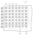
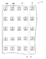
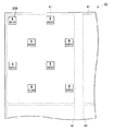
まず、本発明の第1の実施の形態に係る発光装置1について説明する。図1は、発光装置1の平面構成の一例を表したものである。発光装置1は、いわゆるLEDディスプレイと呼ばれる表示装置の表示パネルに好適に適用可能なものである。発光装置1は、図1に示したように、1枚の配線基板10と、この配線基板10上に行列状に実装された複数の発光素子20とを備えたものである。なお、図1では、配線基板10の各種配線が省略されている。
<1. First Embodiment>
[Constitution]
First, the
(発光素子20)
各発光素子20は、所定の波長帯の光を上面から発するチップ状の固体発光素子(半導体素子)であり、具体的には、LEDチップである。LEDチップとは、結晶成長に用いたウェハから切り出した状態のものを指しており、取り出し面を球面上に成形した樹脂などで被われたパッケージタイプのものではないことを指している。LEDチップは、例えば、5μm以上、100mm以下のサイズとなっており、いわゆるマイクロLEDと呼ばれるものである。LEDチップの平面形状は、例えば、ほぼ正方形となっている。LEDチップは、薄片状となっており、LEDチップのアスペクト比は、例えば、0.1以上、1未満となっている。
(Light emitting element 20)
Each
各発光素子20は、互いに近接する複数の発光素子20ごとにグループを構成している。具体的には、図1に示したように、各発光素子20は、列方向に互いに近接する3つの発光素子20ごとにグループGi(iは正の整数)を構成している。各グループGiに含まれる3つの発光素子20は、赤色帯の光を発する発光素子20Rと、緑色帯の光を発する発光素子20Gと、青色帯の光を発する発光素子20Bとにより構成されている。
Each
発光素子20Rは、例えば、グループGi内の他の発光素子20G,Bとの関係で、列の一端に配置されており、発光素子20Bは、例えば、グループGi内の他の発光素子20R,Gとの関係で、列の他端に配置されている。発光素子20Gは、例えば、発光素子20Rと発光素子20Bとの間に配置されている。従って、発光素子20R,20G,20Bは、列方向に周期的に配置されている。発光素子20R,20Gにだけ着目すると、発光素子20R,20Gは、列方向に交互に配置されている。同様に、発光素子20R,20Bにだけ着目すると、発光素子20R,20Bは、列方向に交互に配置されており、発光素子20G,20Bにだけ着目すると、発光素子20G,20Bは、列方向に交互に配置されている。なお、発光素子20R,20G,20Bのそれぞれの位置は、上記に限定されるものではない。
For example, the
図2(A)は、発光素子20の上面構成の一例を表したものである。図2(B)は、図2(A)の発光素子20のA−A矢視方向の断面構成の一例を表したものである。各発光素子20は、例えば、図2(B)に示したように、第1導電型層21、活性層22および第2導電型層23を順に積層してなる半導体積層構造を有している。各発光素子20の上面(具体的には第2導電型層23の上面)が、活性層22から発せられた光を射出する光射出面20Aとなっている。
FIG. 2A illustrates an example of a top surface structure of the
発光素子20Rにおいて、第1導電型層21、活性層22および第2導電型層23は、InP系化合物半導体からなり、例えば、GaInP、AlGaInP、またはAlInPなどによって構成されている。発光素子20Rは、GaAs基板を結晶成長基板として結晶成長させたものである。つまり、発光素子20Rの第1導電型層21、活性層22および第2導電型層23(第2導電型層23にコンタクト層(図示せず)が含まれている場合にはコンタクト層は除く。)は単結晶によって構成されている。発光素子20Rでは、結晶成長基板上にInP系化合物半導体を結晶成長させる際に、結晶成長基板の結晶成長面にはオフ角が設けられており、例えば、図3(A)に示したように、発光素子20Rの結晶軸AX1が発光素子20Rの積層面の法線AX2との関係で、例えば8°〜20°の範囲内で傾いている。そのため、発光素子20Rでも、ファセットが非対称となっている。なお、結晶軸AX1は、例えば、<001>軸であり、積層面の法線から、オフ角の分だけ傾いた方向を向いている。つまり、結晶軸AX1は、発光素子20Rの積層面の面内方向にベクトル成分を持っている。
In the
一方、発光素子20G,20Bにおいて、第1導電型層21、活性層22および第2導電型層23は、ウルツ鉱型の結晶構造を有する窒化物半導体材料からなり、例えば、InGaN系の半導体材料によって構成されている。発光素子20G,20Bは、サファイア基板またはGaN基板を結晶成長基板として結晶成長させたものである。つまり、発光素子20G,20Bの第1導電型層21、活性層22および第2導電型層23(第2導電型層23にコンタクト層(図示せず)が含まれている場合にはコンタクト層は除く。)は単結晶によって構成されている。発光素子20G,20Bでは、結晶成長基板上に窒化物半導体材料を結晶成長させる際に、結晶成長基板の結晶成長面にはオフ角が設けられており、例えば、図3(B)に示したように、発光素子20G,20Bの結晶軸AX3が発光素子20G,20Bの積層面の法線AX4との関係で、例えば0.4°程度傾いている。そのため、発光素子20G,20Bでは、ファセットが若干、非対称となっている。なお、結晶軸AX3は、例えば、C軸であり、積層面の法線から、オフ角の分だけ傾いた方向を向いている。つまり、結晶軸AX3は、発光素子20G,20Bの積層面の面内方向にベクトル成分を持っている。
On the other hand, in the
各発光素子20には、発光素子20に電流を注入するための一対の電極24,25が設けられている。電極24は第2導電型層23と電気的に接続されており、電極25は第1導電型層21と電気的に接続されている。電極24は、例えば、発光素子20の上面(具体的には第2導電型層23の上面)に接して形成されており、電極25は、例えば、発光素子20の下面(具体的には第1導電型層21の下面)に接して形成されている。
Each
なお、電極24,25の位置は、上記の位置に限定されるものではない。例えば、電極24,25がともに、発光素子20の上面または下面に設けられていてもよい。ただし、以下では、電極24,25が図2(A),(B)に示した位置に配置されているものとして、種々の説明を行うものとする。
The positions of the
電極24,25は、発光素子20の面内の中心を中心軸として発光素子20を面内で回転させたときに、例えば、90°回転対称または180°回転対称となっている。電極24,25が90°回転対称となっている場合、電極24,25は、例えば、正方形状となっている。また、電極24,25が180°回転対称となっている場合、電極24,25は、例えば、長方形状となっている。なお、電極24が90°回転対称となっており、電極25が180°回転対称となっていてもよい。また、電極24が180°回転対称となっており、電極25が90°回転対称となっていてもよい。
The
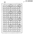
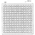
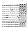
次に、各発光素子20R,20G,20Bの結晶軸の向きについて説明する。図4〜図9は、各発光素子20R,20G,20Bの結晶軸の面内レイアウトの一例を表したものである。図中で20Rと記載された箱の中にある矢印は、各発光素子20Rに共通する1つの結晶軸の向きを表しており、例えば、<001>軸の向きを表している。また、図中で20Gと記載された箱の中にある矢印は、各発光素子20Gに共通する1つの結晶軸の向きを表しており、例えば、C軸の向きを表している。同様に、図中で20Bと記載された箱の中にある矢印は、各発光素子20Bに共通する1つの結晶軸の向きを表しており、例えば、C軸の向きを表している。
Next, the orientation of the crystal axes of the
なお、正確には、図中の矢印は、ある結晶軸を矢印で表したときに、その矢印を平面上に投影したときの、その矢印の向きを表している。本明細書において、結晶軸の向きについて言及している箇所があるが、そのときの結晶軸の向きとは、実際には、ある結晶軸を矢印で表したときに、その矢印を平面(例えばパネル面)上に投影したときの、その矢印の向きを意味している。 To be precise, the arrow in the figure represents the direction of the arrow when a certain crystal axis is represented by an arrow and the arrow is projected onto a plane. In this specification, there is a place where the direction of the crystal axis is referred to. The direction of the crystal axis at this time is actually the direction of the crystal axis when the arrow is represented by an arrow (for example, This means the direction of the arrow when projected onto the panel surface.
本実施の形態では、所定の領域α内に属する同一種類(同一発光色)の複数の発光素子20に着目したときに、行方向および列方向のうち少なくとも一方の方向に互いに近接する同一種類(同一発光色)の発光素子20同士の共通の結晶軸の向きが互いに異なる方向を向いている。ここで、所定の領域α内において行方向および列方向のうち少なくとも一方の方向に互いに近接する同一種類(同一発光色)の発光素子20同士の共通の結晶軸の向きは、90°±5°の範囲内または180°±5°の範囲内で異なっていることがより好ましい。上記の「±5°」は、後述の転写プロセスにおける転写誤差などを考慮したものである。なお、例えば、図中の一番左側の列において、20Rと記載された箱の中にある矢印と、20Gと記載された箱の中にある矢印と、20Bと記載された箱の中にある矢印とが全て、同一の方向を向いているが、互いに同一の方向を向いている必要はない。
In the present embodiment, when attention is paid to a plurality of
なお、上記の領域αは、発光装置1において、製造過程で不具合の発見された発光素子20のリペアをするなど、通常の実装方法(例えば転写)とは異なる方法(例えば手作業)で実装のなされた発光素子20が存在する場合に、そのような発光素子20を除く趣旨で規定されている。従って、上記の領域αは、発光装置1に含まれる複数の発光素子20のうち、通常の実装方法(例えば転写)とは異なる方法(例えば手作業)で実装のなされた発光素子20を除いた全ての発光素子20を含む領域に対応していることが好ましい。
In the
例えば、図4,図5に示した例では、所定の領域α内に属する同一種類(同一発光色)の複数の発光素子20に着目したときに、行方向に互いに近接する同一種類(同一発光色)の発光素子20同士の共通の結晶軸の向きが互いに180°異なる方向を向いている。さらに、図4,図5に示した例では、所定の領域α内に属する同一種類(同一発光色)の複数の発光素子20に着目したときに、列方向に互いに近接する同一種類(同一発光色)の発光素子20同士の共通の結晶軸の向きが互いに同一方向を向いている。例えば、図4,図5に示した例では、同一種類(同一発光色)の複数の発光素子20によって構成される行列のうち互いに近接する2つの列Lv1,Lv2に着目したときに(図では隣接する2つの列に着目している。)、列Lv1と列Lv2とにおいて、共通の結晶軸の向きが互いに異なる(具体的には180°異なる)方向を向いている。また、図4では、1列ごとに、共通の結晶軸の向きが交互に入れ替わっており、図5では、2列ごとに、共通の結晶軸の向きが交互に入れ替わっている。なお、図示しないが、3列以上ごとに、共通の結晶軸の向きが交互に入れ替わっていてもよい。
For example, in the example shown in FIGS. 4 and 5, when attention is paid to a plurality of
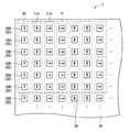
また、例えば、図6,7に示した例では、所定の領域α内に属する同一種類(同一発光色)の複数の発光素子20に着目したときに、行方向に互いに近接する同一種類(同一発光色)の発光素子20同士の共通の結晶軸の向きが互いに90°異なる方向を向いている。さらに、図6,7に示した例では、所定の領域α内に属する同一種類(同一発光色)の複数の発光素子20に着目したときに、列方向に互いに近接する同一種類(同一発光色)の発光素子20同士の共通の結晶軸の向きが互いに同一方向を向いている。例えば、図6,7に示した例では、同一種類(同一発光色)の複数の発光素子20によって構成される行列のうち互いに近接する2つの列Lv3,Lv4に着目したときに(図では隣接する2つの列に着目している。)、列Lv3と列Lv4とにおいて、共通の結晶軸の向きが互いに異なる(具体的には90°異なる)方向を向いている。また、図6では、1列ごとに、共通の結晶軸の向きが交互に入れ替わっており、図7では、2列ごとに、共通の結晶軸の向きが交互に入れ替わっている。なお、図示しないが、3列以上ごとに、共通の結晶軸の向きが交互に入れ替わっていてもよい。
For example, in the examples shown in FIGS. 6 and 7, when attention is paid to a plurality of
また、例えば、図8に示した例では、所定の領域α内に属する同一種類(同一発光色)の複数の発光素子20に着目したときに、行方向に互いに近接する同一種類(同一発光色)の発光素子20同士の共通の結晶軸の向きが互いに180°異なる方向を向いている。さらに、図8に示した例では、所定の領域α内に属する同一種類(同一発光色)の複数の発光素子20に着目したときに、列方向に互いに近接する同一種類(同一発光色)の発光素子20同士の共通の結晶軸の向きも互いに180°異なる方向を向いている。例えば、図8に示した例では、同一種類(同一発光色)の複数の発光素子20によって構成される行列のうち互いに隣接する列Lv5および列Lv6に着目したときに、列Lv5および列Lv6に含まれる同一種類(同一発光色)の全ての発光素子20の共通の結晶軸の面内レイアウトにおいて、互いに隣り合う結晶軸の向きは互いに異なる(具体的には180°異なる)方向を向いている。また、図8では、互いに隣接する2列ごとに、共通の結晶軸の向きが互いに等しい発光素子20が互い違いに配置されている。
Further, for example, in the example shown in FIG. 8, when attention is paid to a plurality of
また、例えば、図9に示した例では、所定の領域α内に属する同一種類(同一発光色)の複数の発光素子20に着目したときに、行方向に互いに近接する同一種類(同一発光色)の発光素子20同士の共通の結晶軸の向きが互いに90°異なる方向を向いている。さらに、図9に示した例では、所定の領域α内に属する同一種類(同一発光色)の複数の発光素子20に着目したときに、列方向に互いに近接する同一種類(同一発光色)の発光素子20同士の共通の結晶軸の向きも互いに90°異なる方向を向いている。例えば、図9に示した例では、同一種類(同一発光色)の複数の発光素子20によって構成される行列のうち互いに隣接する列Lv7および列Lv8に着目したときに、列Lv7および列Lv8に含まれる同一種類(同一発光色)の全ての発光素子20の共通の結晶軸の面内レイアウトにおいて、互いに隣り合う結晶軸の向きは互いに異なる(具体的には90°異なる)方向を向いている。また、図9では、互いに隣接する2列ごとに、共通の結晶軸の向きの互いに等しい発光素子20が互い違いに配置されている。
Further, for example, in the example shown in FIG. 9, when attention is paid to a plurality of
(配線基板10)
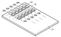
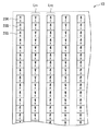
配線基板10は、例えば、図10(A)に示したように、支持基板11上に、一対のパッド電極12,13がマトリクス状(格子状)に配置されたものである。なお、一対のパッド電極12,13はハニカム状に配置されていてもよい。各発光素子20は、パッド電極13上に配置されている。従って、複数の発光素子20も、一対のパッド電極12,13と同様の配列となっており、具体的には、マトリクス状(格子状)またはハニカム状に配置されている。各発光素子20の電極25がパッド電極13に電気的に接続されており、各発光素子20の電極24がパッド電極12に電気的に接続されている。電極25とパッド電極13との接続には、例えば、半田が用いられており、電極24とパッド電極12との接続には、例えば、ワイヤビルドアップ配線が用いられている。
(Wiring board 10)
For example, as illustrated in FIG. 10A, the
なお、配線基板10は、さらに、例えば、図10(B)に示したように、支持基板11上に配線が設けられたものであってもよい。配線基板10は、複数のデータ配線14と、複数のスキャン配線15とを備えている。複数のデータ配線14は、例えば、列方向に延在して形成されており、かつ所定のピッチで並列配置されている。一方、複数のスキャン配線15は、例えば、行方向に延在して形成されており、かつ所定のピッチで並列配置されている。ここで、一対のパッド電極12,13が例えば3つごとに、グループにまとめられており、各データ配線14は、各グループに含まれる1つのパッド電極13に電気的に接続されており、各スキャン配線15は、各グループに含まれる1つのパッド電極12に電気的に接続されている。データ配線14およびスキャン配線15は、例えば、Cu(銅)などの導電性材料からなる。また、各データ配線14および各スキャン配線15のレイアウトは、領域α内に属する全ての発光素子20R,20G,20Bとの関係で互いに等しくなっている。つまり、各データ配線14および各スキャン配線15のレイアウトが発光素子20の結晶軸の向きに関係なく、いずれの発光素子20R,20G,20Bとの関係においても互いに等しくなっている。
Note that the
[製造方法]
次に、本実施の形態の発光装置1の製造方法の一例について説明する。
[Production method]
Next, an example of a method for manufacturing the
まず、結晶成長用の基板上に、発光素子20Rのうち電極24以外の部分(発光素子120R)を多数形成したウェハ100Rを用意する(図11(A))。また、結晶成長用の基板上に、発光素子20Gのうち電極24以外の部分(発光素子120G)を多数形成したウェハ100Gを用意する(図11(B))。さらに、結晶成長用の基板上に、発光素子20Bのうち電極24以外の部分(発光素子120B)を多数形成したウェハ100Bを用意する(図11(C))。なお、発光素子120R,120G,120Bはそれぞれ、第2導電型層23、活性層22、第1導電型層21および電極25が結晶成長用の基板側からこの順に積層された構造となっており、かつ断面が台形状となる形状となっている。つまり、この段階で、第2導電型層23、活性層22および第1導電型層21が、発光素子120R,120G,120Bごとに分離されている。
First, a
また、ウェハ100R上の発光素子120Rを一時的に仮固定するための仮固定用基板200Rを用意する(図12(A))。同様に、ウェハ100G上の発光素子120Gを一時的に仮固定するための仮固定用基板200Gと、ウェハ100B上の発光素子120Bを一時的に仮固定するための仮固定用基板200Bを用意する(図12(B),(C))。仮固定用基板200R,200G,200Bは、例えば、透明基板(例えば石英基板またはサファイア基板)上に、未硬化の接着層が配置されたものである。
Further, a
次に、ウェハ100Rおよび仮固定用基板200Rを、ウェハ100R上の各発光素子120Rが仮固定用基板200R上の接着層と接するように貼り合わせたのち、接着層を硬化させる。続いて、ウェハ100Rの基板を例えばラッピングなどによって除去して、第2導電型層23を露出させる。その後、露出した第2導電型層23上に電極24を形成する。このようにして、仮固定用基板200R上に、複数の発光素子20Rが形成される。
Next, the
また、ウェハ100Gおよび仮固定用基板200Gを、ウェハ100G上の各発光素子120Gが仮固定用基板200G上の接着層と接するように貼り合わせたのち、接着層を硬化させる。続いて、ウェハ100Gの基板を例えばレーザ照射などによって除去して、第2導電型層23を露出させる。その後、露出した第2導電型層23上に電極24を形成する。このようにして、仮固定用基板200G上に、複数の発光素子20Gが形成される。
Further, the
同様に、ウェハ100Bおよび仮固定用基板200Bを、ウェハ100B上の各発光素子120Bが仮固定用基板200B上の接着層と接するように貼り合わせたのち、接着層を硬化させる。続いて、ウェハ100Bの基板を例えばレーザ照射などによって除去して、第2導電型層23を露出させる。その後、露出した第2導電型層23上に電極24を形成する。このようにして、仮固定用基板200B上に、複数の発光素子20Bが形成される。
Similarly, the
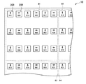
次に、発光素子20R,20G,20Bを実装する配線基板10を用意する(図10(A)または図10(B))。続いて、配線基板10のパッド電極13上に、発光素子20R,20G,20Bを実装する。具体的には、仮固定用基板200Rおよび配線基板10を互いに貼り合わせたのち、レーザ照射により発光素子20Rを仮固定用基板200Rから剥離する。このとき、仮固定用基板200R上の全ての発光素子20Rに対して同時にレーザ照射するのではなく、仮固定用基板200R上の一部の発光素子20Rに対してレーザ照射する。簡単に言えば、間引き転写を行う。例えば、図13に示したように、仮固定用基板200R上の全ての発光素子20Rを複数のブロックB1,B2,…i,…(iは正の整数)に分け、ブロックBiごとに1つずつ、発光素子20Rをレーザ照射により剥離する。このようにして、発光素子20Rが、広いピッチで、配線基板10に転写される。このとき、発光素子20Rは、所定の位置のパッド電極13の直上に配置される(図14)。さらに、同様の方法によって、仮固定用基板200G上の発光素子20Gと、仮固定用基板200B上の発光素子20Bが配線基板10の表面に転写される(図15)。なお、図14、図15では、配線基板10は、図10(A)に記載の態様のものだけでなく、図10(B)に記載の態様のものも含まれる。
Next, the
なお、上記の実装方法では、発光素子20R,20G,20Bの上面(つまり電極24側の面)が配線基板10側を向くことになる。発光素子20R,20G,20Bの上面(つまり電極24側の面)が配線基板10とは反対側を向くようにしたい場合には、例えば、発光素子20R,20G,20Bを配線基板10に実装する前に、再度、発光素子20R,20G,20Bを仮固定基板に転写して、発光素子20R,20G,20Bの上下を反転させておき、その上で、各発光素子20R,20G,20Bを配線基板10に実装すればよい。
In the mounting method described above, the upper surfaces (that is, the surfaces on the
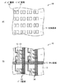
また、図10(A)に記載の配線基板10上に複数の発光素子20R,20G,20Bを形成した場合に、例えば、図16に示したように、互いに近接する3つの発光素子20R,20G,20Bごとに、3つの発光素子20R,20G,20Bを樹脂で覆い、微小パッケージPを形成してもよい。このとき、発光素子20R,20G,20Bの上面(つまり電極24側の面)は配線基板10側を向いていてもよいし、配線基板10とは反対側を向いていてもよい。
Further, when a plurality of
上記のように微小パッケージPを形成した場合には、さらに、微小パッケージPごとに分離し、分離した微小パッケージPを別の配線基板上に実装するようにしてもよい。例えば、まず、配線基板11上の全ての微小パッケージPを一時的に仮固定するための仮固定用基板を用意する。次に、その仮固定用基板と、複数の微小パッケージPの形成された配線基板10とを互いに貼り合わせたのち、例えばレーザ照射などを用いて微小パッケージPを配線基板10の基材から剥離する。次に、微小パッケージPの仮固定された仮固定用基板と新たに用意した配線基板とを互いに貼り合わせたのち、例えばレーザ照射などを用いて微小パッケージPを仮固定用基板から剥離し、配線基板に実装する。このとき新たに用意した配線基板が、例えば、図10(B)に示した配線基板10と同様、一対のパッド電極12,13がマトリクス状に配置されるとともに、複数のデータ配線14が列方向に延在して形成され、かつ複数のスキャン配線15が行方向に延在して形成されたものであることが好ましい。なお、一対のパッド電極12,13はハニカム状に配置されていてもよい。
When the micro package P is formed as described above, it may be further separated for each micro package P, and the separated micro package P may be mounted on another wiring board. For example, first, a temporary fixing substrate for temporarily fixing all the minute packages P on the
なお、上記のプロセスを経て、微小パッケージPを配線基板に実装したときに、微小パッケージPの上下面の向きが所望の向きとは反対になってしまう場合には、例えば、微小パッケージPを配線基板に実装する前に、再度、微小パッケージPを仮固定基板に転写して、微小パッケージPの上下を反転させておき、その上で、微小パッケージPを配線基板に実装すればよい。 In addition, when the micro package P is mounted on the wiring board through the above process, if the orientation of the upper and lower surfaces of the micro package P is opposite to the desired direction, for example, the micro package P is wired. Prior to mounting on the substrate, the micro package P is again transferred to the temporarily fixed substrate, the micro package P is turned upside down, and then the micro package P is mounted on the wiring substrate.
ところで、本実施の形態では、発光素子20R,20G,20Bを配線基板10上に実装する際に、少なくとも上述の領域αに含まれる発光素子20Rにおいて、結晶軸の向きが面内で揃わないようにしている。同様に、少なくとも上述の領域αに含まれる発光素子20Gにおいて、結晶軸の向きが面内で揃わないようにするとともに、少なくとも上述の領域αに含まれる発光素子20Bにおいて、結晶軸の向きが面内で揃わないようにしている。
By the way, in the present embodiment, when the
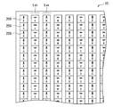
例えば、複数の発光素子120Rが形成されたウェハ300を用意する(図17)。このとき、各発光素子120Rの1つの結晶軸の向き(図中の矢印)が同一の方向を向いている。なお、図17には、各素子の座標が、結晶軸の向きを示す矢印とともに記載されている。次に、ウェハ300上の全ての発光素子120Rを仮固定基板400に転写したのち、上述した方法と同様の方法を用いて発光素子20Rを形成する(図18)。仮固定用基板400は、例えば、透明基板(例えば石英基板またはサファイア基板)上に、未硬化の接着層が配置されたものである。なお、転写に伴い図18中の各素子の座標が図17中の座標を反転させた状態になっている。
For example, a
次に、仮固定用基板400上の複数の発光素子20Rのうち特定の発光素子20R(図18中で丸で囲んだ素子)だけを配線基板10上の所定の領域a1内に転写する(図19)。例えば、特定の列(例えば右から1,5)に含まれる複数の発光素子20Rのうち3つの発光素子20Rごとに1つずつ、配線基板10上に転写する。次に、仮固定用基板400を180°回転させて、仮固定用基板400上の各発光素子20Rの結晶軸の向きを180°回転させたのち、仮固定用基板400上の複数の発光素子20Rのうち特定の発光素子20Rだけを配線基板10上の所定の領域a1内に転写する(図20)。例えば、既に転写の行われた列とは異なる列(例えば図18において左から1,5列)に含まれる複数の発光素子20Rのうち3つの発光素子20Rごとに1つずつ、配線基板10上の発光素子20R同士の間に転写する。同様にして、配線基板10上の他の領域a2,a3,a4,…に対しても、発光素子20Rを転写する(図21)さらに、同様にして、配線基板10上に、発光素子20G,20Bを転写する(図22)。
Next, only a specific
その結果、同一種類(同一発光色)の複数の発光素子20に着目したときに、行方向に互いに近接する同一種類(同一発光色)の発光素子20同士の共通の結晶軸の向きが互いに180°異なる方向を向く。さらに、同一種類(同一発光色)の複数の発光素子20に着目したときに、列方向に互いに近接する同一種類(同一発光色)の発光素子20同士の共通の結晶軸の向きが互いに同一方向を向く。同一種類(同一発光色)の複数の発光素子20によって構成される行列のうち互いに近接する2つの列Lv1,Lv2に着目したときに(図では隣接する2つの列に着目している。)、列Lv1と列Lv2とにおいて、共通の結晶軸の向きが互いに異なる(具体的には180°異なる)方向を向いている。また、1列ごとに、共通の結晶軸の向きが交互に入れ替わっている。このようにして、本実施の形態の発光装置1が製造される。
As a result, when attention is paid to a plurality of
なお、上記と同様の方法を用いて、例えば、図23に示したように、2列ごとに、共通の結晶軸の向きを交互に入れ替えるようにしてもよい。また、図示しないが、3列以上ごとに、共通の結晶軸の向きを交互に入れ替えるようにしてもよい。 Note that, using the same method as described above, for example, as shown in FIG. 23, the orientations of the common crystal axes may be alternately switched every two rows. Although not shown, the orientation of the common crystal axis may be alternately switched every three or more rows.
また、発光素子20Rを配線基板10上に実装したときに、発光素子20Rの上面(つまり電極24側の面)が配線基板10とは反対側を向くようにしたい場合には、例えば、発光素子20Rを配線基板10に実装する前に、再度、発光素子20Rを仮固定基板に転写して、発光素子20Rの上下を反転させておき、その上で、特定の発光素子20Rを配線基板10に実装すればよい。
For example, when the
また、例えば、以下のようにしても、本実施の形態の発光装置1を製造することができる。
Also, for example, the
(その1)
まず、複数の発光素子120Rが形成されたウェハ500を用意する(図24)。このとき、各発光素子120Rの1つの結晶軸の向き(図中の矢印)が同一の方向を向いている。なお、図24には、各素子の座標が、結晶軸の向きを示す矢印とともに記載されている。次に、ウェハ500上の全ての発光素子120Rを仮固定基板600に転写したのち、上述した方法と同様の方法を用いて発光素子20Rを形成する(図25)。仮固定用基板600は、例えば、透明基板(例えば石英基板またはサファイア基板)上に、未硬化の接着層が配置されたものである。なお、転写に伴い図25中の各素子の座標が図24中の座標を左右反転させた状態になっている。
(Part 1)
First, a wafer 500 having a plurality of
次に、仮固定用基板600上の複数の発光素子20Rのうち特定の発光素子20R(図25中で丸で囲んだ素子)だけを配線基板10上の所定の領域a1内に転写する(図26)。例えば、特定の列(例えば右から1,4,7列)に含まれる複数の発光素子20Rのうち3つの発光素子20Rごとに1つずつ、配線基板10上に転写する。次に、仮固定用基板600を90°回転させて、仮固定用基板600上の各発光素子20Rの結晶軸の向きを90°回転させたのち、仮固定用基板600上の複数の発光素子20Rのうち特定の発光素子20Rだけを配線基板10上の所定の領域a1内に転写する(図27)。例えば、既に転写の行われた列とは異なる列(例えば図25において左から1,4,7列)に含まれる複数の発光素子20Rのうち3つの発光素子20Rごとに1つずつ、配線基板10上の発光素子20R同士の間に転写する。同様にして、配線基板10上の他の領域a2,a3,a4,…に対しても、発光素子20Rを転写する(図28)さらに、同様にして、配線基板10上に、発光素子20G,20Bを転写する(図29)。
Next, only a specific
その結果、同一種類(同一発光色)の複数の発光素子20に着目したときに、行方向に互いに近接する同一種類(同一発光色)の発光素子20同士の共通の結晶軸の向きが互いに90°異なる方向を向く。さらに、同一種類(同一発光色)の複数の発光素子20に着目したときに、列方向に互いに近接する同一種類(同一発光色)の発光素子20同士の共通の結晶軸の向きが互いに同一方向を向く。同一種類(同一発光色)の複数の発光素子20によって構成される行列のうち互いに近接する2つの列Lv3,Lv4に着目したときに(図では隣接する2つの列に着目している。)、列Lv3と列Lv4とにおいて、共通の結晶軸の向きが互いに異なる(具体的には90°異なる)方向を向いている。また、1列ごとに、共通の結晶軸の向きが交互に入れ替わっている。
As a result, when attention is paid to a plurality of
なお、上記と同様の方法を用いて、例えば、図30に示したように、2列ごとに、共通の結晶軸の向きを交互に入れ替えるようにしてもよい。また、図示しないが、3列以上ごとに、共通の結晶軸の向きを交互に入れ替えるようにしてもよい。 Note that, using the same method as described above, for example, as shown in FIG. 30, the direction of the common crystal axis may be alternately changed every two rows. Although not shown, the orientation of the common crystal axis may be alternately switched every three or more rows.
(その2)
まず、複数の発光素子120Rが形成されたウェハ300を用意したのち(図17)、仮固定基板400上に複数の発光素子20Rを形成する(図18)。次に、仮固定用基板400上の複数の発光素子20Rのうち特定の発光素子20R(図31中で丸で囲んだ素子)だけを配線基板10上の所定の領域a1内に転写する(図32)。例えば、特定の列(例えば図32において右から1,3,5,7列)に含まれる複数の発光素子20Rのうち6つの発光素子20Rごとに1つずつ、配線基板10上に転写する。このとき、図32に示したように、各発光素子20Rを互い違いに、配線基板10上に転写する。次に、仮固定用基板400を180°回転させて、仮固定用基板400上の各発光素子20の結晶軸の向きを180°回転させたのち、仮固定用基板400上の複数の発光素子20Rのうち特定の発光素子20R(図33中で丸で囲んだ素子)だけを配線基板10上の所定の領域a1内に転写する(図34)。例えば、特定の列(例えば図33において右から1,3,5,7列)に含まれる複数の発光素子20Rのうち一部の発光素子20Rを互い違いに、配線基板10上に転写する。同様にして、配線基板10上の他の領域a2,a3,a4,…に対しても、発光素子20Rを転写する(図35)さらに、同様にして、配線基板10上に、発光素子20G,20Bを転写する(図36)。
(Part 2)
First, after preparing the
その結果、同一種類(同一発光色)の複数の発光素子20に着目したときに、行方向に互いに近接する同一種類(同一発光色)の発光素子20同士の共通の結晶軸の向きが互いに180°異なる方向を向いている。さらに、同一種類(同一発光色)の複数の発光素子20に着目したときに、列方向に互いに近接する同一種類(同一発光色)の発光素子20同士の共通の結晶軸の向きも互いに180°異なる方向を向いている。例えば、同一種類(同一発光色)の複数の発光素子20によって構成される行列のうち互いに隣接する列Lv5および列Lv6に着目したときに、列Lv5および列Lv6に含まれる同一種類(同一発光色)の全ての発光素子20の共通の結晶軸の面内レイアウトにおいて、互いに隣り合う結晶軸の向きは互いに異なる(具体的には180°異なる)方向を向いている。また、互いに隣接する2列ごとに、共通の結晶軸の向きの互いに等しい発光素子20が互い違いに配置されている。
As a result, when attention is paid to a plurality of
(その3)
まず、複数の発光素子120Rが形成されたウェハ700を用意する(図37)。このとき、各発光素子120Rの1つの結晶軸の向き(図中の矢印)が同一の方向を向いている。なお、図37には、各素子の座標が、結晶軸の向きを示す矢印とともに記載されている。次に、ウェハ700R上の全ての発光素子120Rを仮固定基板800に転写したのち、上述した方法と同様の方法を用いて発光素子20Rを形成する(図38)。仮固定用基板800は、例えば、透明基板(例えば石英基板またはサファイア基板)上に、未硬化の接着層が配置されたものである。なお、転写に伴い図38中の各素子の座標が図37中の座標を左右反転させた状態になっている。
(Part 3)
First, a wafer 700 on which a plurality of
次に、仮固定用基板800上の複数の発光素子20Rのうち特定の発光素子20R(図38中で丸で囲んだ素子)だけを配線基板10上の所定の領域a1内に転写する(図39)。例えば、特定の列(例えば右から1,4,7,10列)に含まれる複数の発光素子20Rのうち6つの発光素子20Rごとに1つずつ、配線基板10上に転写する。このとき、図39に示したように、各発光素子20Rを互い違いに、配線基板10上に転写する。次に、仮固定用基板800を90°回転させて、仮固定用基板800上の各発光素子20Rの結晶軸の向きを90°回転させたのち、仮固定用基板800上の複数の発光素子20Rのうち特定の発光素子20R(図40中で丸で囲んだ素子)だけを配線基板10上の所定の領域a1内に転写する(図41)。例えば、既に転写の行われた列とは異なる列(例えば図40において左から1,4,7,10列)に含まれる複数の発光素子20Rのうち6つの発光素子20Rごとに1つずつ、配線基板10上の発光素子20R同士の間に転写する。このとき、図41に示したように、各発光素子20Rを互い違いに、配線基板10上に転写する。同様にして、配線基板10上の他の領域a2,a3,a4,…に対しても、発光素子20Rを転写する(図42)さらに、同様にして、配線基板10上に、発光素子20G,20Bを転写する(図43)。
Next, only a specific
その結果、同一種類(同一発光色)の複数の発光素子20に着目したときに、行方向に互いに近接する同一種類(同一発光色)の発光素子20同士の共通の結晶軸の向きが互いに90°異なる方向を向いている。さらに、同一種類(同一発光色)の複数の発光素子20に着目したときに、列方向に互いに近接する同一種類(同一発光色)の発光素子20同士の共通の結晶軸の向きも互いに90°異なる方向を向いている。例えば、同一種類(同一発光色)の複数の発光素子20によって構成される行列のうち互いに隣接する列Lv7および列Lv8に着目したときに、列Lv7および列Lv8に含まれる同一種類(同一発光色)の全ての発光素子20の共通の結晶軸の面内レイアウトにおいて、互いに隣り合う結晶軸の向きは互いに異なる(具体的には90°異なる)方向を向いている。また、互いに隣接する2列ごとに、共通の結晶軸の向きの互いに等しい発光素子20が互い違いに配置されている。
As a result, when attention is paid to a plurality of
なお、上述した3つの転写プロセスにおいて、発光素子20Rを配線基板10上に実装したときに、発光素子20Rの上面(つまり電極24側の面)が配線基板10とは反対側を向くようにしたい場合には、例えば、発光素子20Rを配線基板10に実装する前に、再度、発光素子20Rを仮固定基板に転写して、発光素子20Rの上下を反転させておき、その上で、特定の発光素子20Rを配線基板10に実装すればよい。
In the three transfer processes described above, when the
[効果]
本実施の形態では、共通の配線基板10上に行列状に実装された各発光素子20Rの結晶軸の向きが全て同じ方向を向いておらず、行方向および列方向のうち少なくとも一方の方向に互いに近接する発光素子20R同士の共通の結晶軸の向きが互いに異なる方向を向いている。また、共通の配線基板10上に行列状に実装された各発光素子20Gの結晶軸の向きが全て同じ方向を向いておらず、行方向および列方向のうち少なくとも一方の方向に互いに近接する発光素子20G同士の共通の結晶軸の向きが互いに異なる方向を向いている。さらに、共通の配線基板10上に行列状に実装された各発光素子20Bの結晶軸の向きが全て同じ方向を向いておらず、行方向および列方向のうち少なくとも一方の方向に互いに近接する発光素子20B同士の共通の結晶軸の向きが互いに異なる方向を向いている。
[effect]
In the present embodiment, the crystal axes of the
これにより、各赤色LEDの放射角の傾きが面内で揃わなくなり、緑色LEDの表面に形成された縞模様が面内で揃わなくなり、さらに、青色LEDの表面に形成された縞模様も面内で揃わなくなる。その結果、赤色LEDの結晶軸の向きが面内で揃うとともに、緑色LEDの結晶軸の向きが面内で揃い、青色LEDの結晶軸の向きが面内で揃っている場合と比べて、面内でのFFP(Far Field Pattern)の偏りを少なくすることができるので、色むらや輝度むらを改善することができる。なお、素子の結晶軸の向きが主軸からずれることで、ピエゾ電解が発生し、また偏光性が出るが、本実施の形態では、偏光性が打ち消し合うので発光装置1全体としてはムラのないものができる。
Thereby, the inclination of the emission angle of each red LED is not aligned in the plane, the striped pattern formed on the surface of the green LED is not aligned in the plane, and the striped pattern formed on the surface of the blue LED is also in-plane. Will not be complete. As a result, the direction of the crystal axis of the red LED is aligned in the plane, the direction of the crystal axis of the green LED is aligned in the plane, and the direction of the crystal axis of the blue LED is aligned in the plane. The unevenness of FFP (Far Field Pattern) can be reduced, so that uneven color and uneven brightness can be improved. In addition, although the direction of the crystal axis of the element deviates from the main axis, piezoelectrolysis occurs, and the polarization is generated. However, in this embodiment, since the polarization cancels out, the
<2.第1の実施の形態の変形例>
上記実施の形態では、全ての色のLEDの結晶軸の向きが面内で揃わないようにしていたが、例えば、3色のLEDのうち1色のLEDの結晶軸の向きだけが面内で揃わないようにしてもよい。例えば、赤色のLEDの結晶軸の向きだけが面内で揃わないようにしてもよいし、緑色のLEDの結晶軸の向きだけが面内で揃わないようにしてもよいし、青色のLEDの結晶軸の向きだけが面内で揃わないようにしてもよい。また、例えば、3色のLEDのうち2色のLEDの結晶軸の向きだけが面内で揃わないようにしてもよい。例えば、赤色のLEDと緑色のLEDの結晶軸の向きだけが面内で揃わないようにしてもよいし、赤色のLEDと青色のLEDの結晶軸の向きだけが面内で揃わないようにしてもよいし、緑色のLEDと青色のLEDの結晶軸の向きだけが面内で揃わないようにしてもよい。
<2. Modification of First Embodiment>
In the above embodiment, the orientations of the crystal axes of the LEDs of all colors are not aligned in the plane. For example, only the orientation of the crystal axes of the LEDs of one color among the three colors of LEDs is in the plane. You may make it not align. For example, only the crystal axis direction of the red LED may not be aligned in the plane, only the crystal axis direction of the green LED may not be aligned in the plane, Only the orientation of the crystal axes may not be aligned in the plane. Further, for example, only the crystal axis orientations of the two color LEDs out of the three color LEDs may not be aligned in the plane. For example, only the crystal axes of red and green LEDs may not be aligned in the plane, or only the crystal axes of red and blue LEDs may not be aligned in the plane. Alternatively, only the crystal axes of the green LED and the blue LED may not be aligned in the plane.
また、上記実施の形態およびその変形例では、発光装置1は、グループGiごとに3色の発光素子(LED)を備えていたが、4色の発光素子(LED)を備えていてもよいし、1色または2色の発光素子(LED)だけを備えていてもよい。発光装置1がグループGiごとに2色の発光素子(LED)だけを備えている場合に、各データ配線14および各スキャン配線15のレイアウトは、例えば、領域α内に属する各色の発光素子(LED)との関係で互いに等しくなっている。
Moreover, in the said embodiment and its modification, although the light-emitting
<3.第2の実施の形態>
[構成]
次に、本発明の第2の実施の形態に係る表示装置2について説明する。表示装置2は、例えば、上記実施の形態に係る1つの発光装置1が表示パネル全面に配置されたものである。なお、表示装置2は、上記実施の形態に係る複数の発光装置1が、表示パネル全面にマトリクス状(格子状)またはハニカム状に配置されたものであってもよい。
<3. Second Embodiment>
[Constitution]
Next, a
図44は、表示装置2の概略構成の一例を斜視的に表したものである。表示装置2は、いわゆるLEDディスプレイと呼ばれるものであり、表示画素としてLEDが用いられたものである。表示装置2は、例えば、図44に示したように、表示パネル210と、表示パネル210を駆動する駆動回路(図示せず)とを備えている。
FIG. 44 is a perspective view showing an example of a schematic configuration of the
(表示パネル210)
表示パネル210は、実装基板210−1と、透明基板210−2とを互いに重ね合わせたものである。透明基板210−2の表面が映像表示面となっており、中央部分に表示領域210Aを有し、その周囲に、非表示領域であるフレーム領域210Bを有している。
(Display panel 210)
The
(実装基板210−1)
図45は、実装基板210−1の透明基板210−2側の表面のうち表示領域210Aに対応する領域のレイアウトの一例を表したものである。実装基板210−1の表面のうち表示領域210Aに対応する領域には、例えば、図45に示したように、複数のデータ配線14が列方向に延在して形成されており、かつ所定のピッチで並列配置されている。実装基板210−1の表面のうち表示領域210Aに対応する領域には、さらに、例えば、複数のスキャン配線15がデータ配線14と交差(例えば直交)する方向に延在して形成されており、かつ所定のピッチで並列配置されている。
(Mounting board 210-1)
FIG. 45 illustrates an example of a layout of a region corresponding to the
スキャン配線15は、例えば、最表層に形成されており、例えば、基材表面に形成された絶縁層(図示せず)上に形成されている。なお、実装基板210−1の基材は、例えば、ガラス基板、または樹脂基板などからなり、基材上の絶縁層は、例えば、SiN、SiO2、またはAl2O3からなる。一方、データ配線14は、スキャン配線15を含む最表層とは異なる層(例えば、最表層よりも下の層)内に形成されており、例えば、基材上の絶縁層内に形成されている。絶縁層の表面上には、スキャン配線15の他に、例えば、必要に応じて、ブラックが設けられている。ブラックは、コントラストを高めるためのものであり、光吸収性の材料によって構成されている。ブラックは、例えば、絶縁層の表面のうち少なくともパッド電極12,13の非形成領域に形成されている。なお、ブラックは、必要に応じて省略することも可能である。
The
データ配線14とスキャン配線15との交差部分の近傍が表示画素16となっており、複数の表示画素16が表示領域210A内においてマトリクス状(格子状)またはハニカム状に配置されている。各表示画素16には、例えば、図45に示したように、複数の発光素子20が実装されている。従って、複数の発光素子20も、表示画素16と同様の配列となっており、具体的には、マトリクス状(格子状)またはハニカム状に配置されている。なお、各発光素子20は、上記実施の形態で既に述べた方法と同一の方法で実装されており、発光素子20の上面(つまり電極24側の面)が透明基板210−2側を向いている。なお、図45には、3つの発光素子20(20R,20G,20B)で一つの表示画素16が構成されており、発光素子20Rから赤色の光を、発光素子20Gから緑色の光を、発光素子20Bから青色の光をそれぞれ出力することができるようになっている場合が例示されている。発光素子20は、例えばLEDチップである。
A
発光素子20には、例えば、図2(A),(B)に示したように、一対の電極24,25が設けられている。そして、電極25がデータ配線14に電気的に接続されており、電極24がスキャン配線15に電気的に接続されている。例えば、電極25は、パッド電極13を介してデータ配線14に接続されている。また、例えば、電極24は、パッド電極12を介してスキャン配線15に接続されている。また、各データ配線14および各スキャン配線15のレイアウトは、領域α内に属する全ての発光素子20R,20G,20Bとの関係で互いに等しくなっている。つまり、各データ配線14および各スキャン配線15のレイアウトが発光素子20の結晶軸の向きに関係なく、いずれの発光素子20R,20G,20Bとの関係においても互いに等しくなっている。
For example, as shown in FIGS. 2A and 2B, the
各パッド電極12,13は、例えば、最表層に形成されており、例えば、図45に示したように、各発光装置1が実装される部位に設けられている。ここで、パッド電極12,13は、例えば、Au(金)などの導電性材料からなる。
Each of the
実装基板210−1には、さらに、例えば、実装基板210−1と透明基板210−2との間の間隔を規制する複数の支柱(図示せず)が設けられている。支柱は、表示領域210Aとの対向領域内に設けられていてもよいし、フレーム領域210Bとの対向領域内に設けられていてもよい。
The mounting substrate 210-1 is further provided with, for example, a plurality of support columns (not shown) that regulate the distance between the mounting substrate 210-1 and the transparent substrate 210-2. The support column may be provided in a region facing the
(透明基板210−2)
透明基板210−2は、例えば、ガラス基板、または樹脂基板などからなる。透明基板210−2において、実装基板210−1側の表面は平坦となっていてもよいが、粗面となっていることが好ましい。粗面は、表示領域210Aとの対向領域全体に渡って設けられていてもよいし、表示画素16との対向領域にだけ設けられていてもよい。粗面は、発光素子20から発せられた光が当該粗面に入射したときに入射光を散乱させる程度に細かな凹凸を有している。粗面の凹凸は、例えば、サンドブラストや、ドライエッチングなどによって作製可能である。
(Transparent substrate 210-2)
The transparent substrate 210-2 is made of, for example, a glass substrate or a resin substrate. In the transparent substrate 210-2, the surface on the mounting substrate 210-1 side may be flat, but is preferably a rough surface. The rough surface may be provided over the entire area facing the
(駆動回路)
駆動回路は、映像信号に基づいて複数の表示画素16を駆動するものである。駆動回路は、例えば、表示画素16に接続されたデータ配線14を駆動するデータドライバと、表示画素16に接続されたスキャン配線15を駆動するスキャンドライバとにより構成されている。駆動回路は、例えば、実装基板210−1上に実装されていてもよいし、表示パネル210とは別体で設けられ、かつ配線(図示せず)を介して実装基板210−1と接続されていてもよい。
(Drive circuit)
The drive circuit drives the plurality of
[表示パネル210の製造方法]
次に、表示パネル210の製造方法の一例について説明する。
[Method for Manufacturing Display Panel 210]
Next, an example of a method for manufacturing the
まず、例えば、基材上に、複数のデータ配線14を内部に含む絶縁層と、配線パターン(スキャン配線15およびパッド電極12,13)とを有する回路基板を用意する。次に、回路基板上に複数の発光素子20を実装する。このとき、上記実施の形態で既に述べた方法と同一の方法で、発光素子20が実装される。これにより、実装基板210−1が形成される。次に、実装基板210−1と透明基板210−2とを互いに向かい合わせ、貼り合わせる。このようにして、表示パネル210が製造される。
First, for example, a circuit board having an insulating layer including a plurality of data wirings 14 and wiring patterns (scanning
[表示装置2の動作・効果]
本実施の形態では、発光素子20が駆動回路によって、データ配線14およびスキャン配線15を介して駆動(例えば単純マトリクス駆動)される。これにより、データ配線14とスキャン配線15との交差部分近傍に設けられた発光素子20に順次、電流が供給され、表示領域210Aに画像が表示される。
[Operation and effect of display device 2]
In the present embodiment, the
ところで、本実施の形態では、表示画素16に使用される発光素子20が上記実施の形態で既に述べた方法と同一の方法で回路基板上に実装される。これにより、各赤色LEDの放射角の傾きが面内で揃わなくなり、緑色LEDの表面に形成された縞模様が面内で揃わなくなり、さらに、青色LEDの表面に形成された縞模様も面内で揃わなくなる。その結果、赤色LEDの結晶軸の向きが面内で揃うとともに、緑色LEDの結晶軸の向きが面内で揃い、青色LEDの結晶軸の向きが面内で揃っている場合と比べて、面内でのFFP(Far Field Pattern)の偏りを少なくすることができるので、色むらや輝度むらを改善することができる。なお、素子の結晶軸の向きが主軸からずれることで、ピエゾ電解が発生し、また偏光性が出るが、本実施の形態では、偏光性が打ち消し合うので表示装置2全体としてはムラのないものができる。
By the way, in this embodiment, the
<4.第2の実施の形態の変形例>
上記第2の実施の形態では、全ての色のLEDの結晶軸の向きが面内で揃わないようにしていたが、例えば、3色のLEDのうち1色のLEDの結晶軸の向きだけが面内で揃わないようにしてもよい。例えば、赤色のLEDの結晶軸の向きだけが面内で揃わないようにしてもよいし、緑色のLEDの結晶軸の向きだけが面内で揃わないようにしてもよいし、青色のLEDの結晶軸の向きだけが面内で揃わないようにしてもよい。また、例えば、3色のLEDのうち2色のLEDの結晶軸の向きだけが面内で揃わないようにしてもよい。例えば、赤色のLEDと緑色のLEDの結晶軸の向きだけが面内で揃わないようにしてもよいし、赤色のLEDと青色のLEDの結晶軸の向きだけが面内で揃わないようにしてもよいし、緑色のLEDと青色のLEDの結晶軸の向きだけが面内で揃わないようにしてもよい。
<4. Modification of Second Embodiment>
In the second embodiment, the orientations of the crystal axes of the LEDs of all colors are not aligned in the plane. For example, only the orientation of the crystal axes of the LEDs of one color among the three colors of LEDs is different. You may make it not align in a plane. For example, only the crystal axis direction of the red LED may not be aligned in the plane, only the crystal axis direction of the green LED may not be aligned in the plane, Only the orientation of the crystal axes may not be aligned in the plane. Further, for example, only the crystal axis orientations of the two color LEDs out of the three color LEDs may not be aligned in the plane. For example, only the crystal axes of red and green LEDs may not be aligned in the plane, or only the crystal axes of red and blue LEDs may not be aligned in the plane. Alternatively, only the crystal axes of the green LED and the blue LED may not be aligned in the plane.
また、上記第2の実施の形態およびその変形例において、ある方向に結晶軸の向きを有する発光素子20と、他の方向に結晶軸の向きを有する発光素子20とが互いに異なる偏光光を出力するようになっていてもよい。例えば、複数の発光素子20R,20G,20Bのうち領域α内に属する複数の発光素子20R,20G,20Bを、列方向において互いに近接する発光素子20R,20G,20Bごとにグループ分けしたときに、一のグループ(例えば一の表示画素16)から発せられる光の偏光成分と、他のグループ(例えば他の表示画素16)から発せられる光の偏光成分とが互いに異なっていてもよい。例えば、各発光素子20R,20G,20Bにおいて、オフ角を90°近くにした場合には、歪の効果により偏光が生じる。このようにした場合には、一方の偏向成分の光で右目用の画像を表示し、他方の偏向成分の光で左目用の画像を表示することにより、偏向眼鏡にシャッターを設けなくても、3D映像を視認することが可能となる。
In the second embodiment and its modification, the
また、上記第2の実施の形態およびその変形例では、表示装置2は、表示画素16として3色のLEDを備えていたが、4色のLEDを備えていてもよいし、1色または2色のLEDだけを備えていてもよい。
Moreover, in the said 2nd Embodiment and its modification, the
<5.第3の実施の形態>
[構成]
次に、本発明の第3の実施の形態に係る照明装置3について説明する。照明装置3は、上記実施の形態に係る発光装置1が照明パネル全面に配置されたものである。なお、照明装置3は、上記実施の形態に係る複数の発光装置1が、照明パネル全面にマトリクス状(格子状)またはハニカム状に配置されたものであってもよい。
<5. Third Embodiment>
[Constitution]
Next, the illuminating
図46は、照明装置3の概略構成の一例を斜視的に表したものである。照明装置3は、いわゆるLED照明と呼ばれるものであり、光源としてLEDが用いられたものである。照明装置3は、例えば、図46に示したように、照明パネル330と、照明パネル330を駆動する駆動回路(図示せず)とを備えている。
FIG. 46 is a perspective view showing an example of a schematic configuration of the
(照明パネル330)
照明パネル330は、実装基板330−1と、透明基板330−2とを互いに重ね合わせたものである。透明基板330−2の表面が、照明光が出力される面となっており、中央部分に照明領域330Aを有している。
(Lighting panel 330)
The
図47は、実装基板330−1の透明基板330−2側の表面のうち照明領域330Aに対応する領域のレイアウトの一例を表したものである。本実施の形態では、図45に記載の表示画素16に対応するものが、照明画素17となる。
FIG. 47 illustrates an example of a layout of a region corresponding to the illumination region 330A on the surface of the mounting substrate 330-1 on the transparent substrate 330-2 side. In the present embodiment, the
(駆動回路)
駆動回路は、複数の照明画素17を駆動するものである。駆動回路は、例えば、照明画素17に接続されたデータ配線14を駆動するデータドライバと、照明画素17に接続されたスキャン配線15を駆動するスキャンドライバとにより構成されている。駆動回路は、例えば、実装基板330−1上に実装されていてもよいし、照明パネル330とは別体で設けられていてもよい。
(Drive circuit)
The drive circuit drives a plurality of
[照明パネル330の製造方法]
次に、照明パネル330の製造方法の一例について説明する。
[Method for Manufacturing Lighting Panel 330]
Next, an example of a method for manufacturing the
まず、例えば、基材上に、複数のデータ配線14を内部に含む絶縁層と、配線パターン(スキャン配線15およびパッド電極12,13)とを有する回路基板を用意する。次に、回路基板上に複数の発光素子20を実装する。このとき、上記実施の形態で既に述べた方法と同一の方法で、発光素子20が実装される。これにより、実装基板330−1が形成される。次に、実装基板330−1と透明基板330−2とを互いに向かい合わせ、貼り合わせる。このようにして、照明パネル330が製造される。
First, for example, a circuit board having an insulating layer including a plurality of data wirings 14 and wiring patterns (scanning
[照明装置3の動作・効果]
本実施の形態では、発光素子20が駆動回路によって、データ配線14およびスキャン配線15によって駆動される。これにより、データ配線14とスキャン配線15との交差部分近傍に設けられた発光素子20に電流が供給され、照明領域330Aから照明光が出力される。
[Operation and effect of lighting device 3]
In the present embodiment, the
ところで、本実施の形態では、照明画素17に使用される発光素子20が上記実施の形態で既に述べた方法と同一の方法で回路基板上に実装される。これにより、各赤色LEDの放射角の傾きが面内で揃わなくなり、緑色LEDの表面に形成された縞模様が面内で揃わなくなり、さらに、青色LEDの表面に形成された縞模様も面内で揃わなくなる。その結果、赤色LEDの結晶軸の向きが面内で揃うとともに、緑色LEDの結晶軸の向きが面内で揃い、青色LEDの結晶軸の向きが面内で揃っている場合と比べて、色むらや輝度むらを改善することができる。なお、素子の結晶軸の向きが主軸からずれることで、ピエゾ電解が発生し、また偏光性が出るが、本実施の形態では、偏光性が打ち消し合うので照明装置3全体としてはムラのないものができる。
By the way, in this embodiment, the
<6.第3の実施の形態の変形例>
上記第3の実施の形態では、全ての色のLEDの結晶軸の向きが面内で揃わないようにしていたが、例えば、3色のLEDのうち1色のLEDの結晶軸の向きだけが面内で揃わないようにしてもよい。例えば、赤色のLEDの結晶軸の向きだけが面内で揃わないようにしてもよいし、緑色のLEDの結晶軸の向きだけが面内で揃わないようにしてもよいし、青色のLEDの結晶軸の向きだけが面内で揃わないようにしてもよい。また、例えば、3色のLEDのうち2色のLEDの結晶軸の向きだけが面内で揃わないようにしてもよい。例えば、赤色のLEDと緑色のLEDの結晶軸の向きだけが面内で揃わないようにしてもよいし、赤色のLEDと青色のLEDの結晶軸の向きだけが面内で揃わないようにしてもよいし、緑色のLEDと青色のLEDの結晶軸の向きだけが面内で揃わないようにしてもよい。
< 6. Modification of Third Embodiment>
In the third embodiment, the orientations of the crystal axes of the LEDs of all colors are not aligned in the plane. For example, only the orientation of the crystal axes of the LEDs of one color among the three colors of LEDs is different. You may make it not align in a plane. For example, only the crystal axis direction of the red LED may not be aligned in the plane, only the crystal axis direction of the green LED may not be aligned in the plane, Only the orientation of the crystal axes may not be aligned in the plane. Further, for example, only the crystal axis orientations of the two color LEDs out of the three color LEDs may not be aligned in the plane. For example, only the crystal axes of red and green LEDs may not be aligned in the plane, or only the crystal axes of red and blue LEDs may not be aligned in the plane. Alternatively, only the crystal axes of the green LED and the blue LED may not be aligned in the plane.
また、上記第3の実施の形態およびその変形例では、照明装置3は、照明画素17として3色のLEDを備えていたが、4色のLEDを備えていてもよいし、1色または2色のLEDだけを備えていてもよい。
Moreover, in the said 3rd Embodiment and its modification, although the illuminating
以上、複数の実施の形態およびそれらの変形例を挙げて本発明を説明したが、本発明は上記実施の形態等に限定されるものではなく、種々変形が可能である。 The present invention has been described above with reference to a plurality of embodiments and their modifications. However, the present invention is not limited to the above-described embodiments and the like, and various modifications can be made.
例えば、上記実施の形態等では、電極24が発光素子20の上面に形成され、電極25が発光素子20の下面に形成されていたが、電極24,25がともに、発光素子20の下面に形成されていてもよい。この場合、例えば、第1導電型層21、活性層22および第2導電型層23に対して柱状メサが形成され、柱状メサの頂部(第1導電型層21)に電極24が電気的に接続され、柱状メサの裾野(第2導電型層23)に電極25が電気的に接続される。第2導電型層23と電極25との電気的な接続には、例えば、柱状バンプなどが用いられる。なお、第1導電型層21と電極24との電気的な接続にも、例えば、柱状バンプなどが用いられてもよい。
For example, in the above-described embodiment and the like, the
以下に、電極24,25がともに、発光素子20の下面に形成されている場合の、発光素子20の転写方法の一例について説明する。まず、結晶成長用の基板上に、発光素子20Rのうち電極24,25以外の部分(発光素子220R(図示せず))を多数形成したウェハ1000R(図示せず)を用意する。また、結晶成長用の基板上に、発光素子20Gのうち電極24,25以外の部分(発光素子220G(図示せず))を多数形成したウェハ1000G(図示せず)を用意する。さらに、結晶成長用の基板上に、発光素子20Bのうち電極24,25以外の部分(発光素子220B(図示せず))を多数形成したウェハ1000B(図示せず)を用意する。なお、発光素子220R,220G,220Bはそれぞれ、第2導電型層23、活性層22および第1導電型層21が結晶成長用の基板側からこの順に積層された構造となっている。なお、この段階では、第2導電型層23、活性層22および第1導電型層21は、発光素子220R,220G,220Bごとに分離されていない。
Hereinafter, an example of a transfer method of the
また、ウェハ1000R上の発光素子220Rを一時的に仮固定するための仮固定用基板2000R(図示せず)を用意する。同様に、ウェハ1000G上の発光素子220Gを一時的に仮固定するための仮固定用基板2000G(図示せず)と、ウェハ1000B上の発光素子220Bを一時的に仮固定するための仮固定用基板200B(図示せず)を用意する。仮固定用基板2000R,2000G,2000Bは、例えば、透明基板(例えば石英基板またはサファイア基板)上に、未硬化の接着層が配置されたものである。 Also, a temporary fixing substrate 2000R (not shown) for temporarily fixing the light emitting element 220R on the wafer 1000R is prepared. Similarly, a temporary fixing substrate 2000G (not shown) for temporarily fixing the light emitting element 220G on the wafer 1000G and a temporary fixing for temporarily fixing the light emitting element 220B on the wafer 1000B. A substrate 200B (not shown) is prepared. For example, the temporary fixing substrates 2000R, 2000G, and 2000B are obtained by disposing an uncured adhesive layer on a transparent substrate (for example, a quartz substrate or a sapphire substrate).
次に、ウェハ1000Rおよび仮固定用基板2000Rを、ウェハ1000R上の各発光素子220Rが仮固定用基板2000R上の接着層と接するように貼り合わせたのち、接着層を硬化させる。続いて、ウェハ1000Rの基板を例えばラッピングなどによって除去して、第2導電型層23を露出させる。その後、露出した第2導電型層23上に電極24,25を形成するとともに、各発光素子220Rを素子分離する。このようにして、仮固定用基板2000R上に、複数の発光素子20Rが形成される。
Next, the wafer 1000R and the temporary fixing substrate 2000R are bonded together so that each light emitting element 220R on the wafer 1000R is in contact with the adhesive layer on the temporary fixing substrate 2000R, and then the adhesive layer is cured. Subsequently, the substrate of the wafer 1000R is removed by, for example, lapping, and the second
また、ウェハ1000Gおよび仮固定用基板2000Gを、ウェハ1000G上の各発光素子220Gが仮固定用基板2000G上の接着層と接するように貼り合わせたのち、接着層を硬化させる。続いて、ウェハ1000Gの基板を例えばレーザ照射などによって除去して、第2導電型層23を露出させる。その後、露出した第2導電型層23上に電極24,25を形成するとともに、各発光素子220Gを素子分離する。このようにして、仮固定用基板2000G上に、複数の発光素子20Gが形成される。
Further, the wafer 1000G and the temporary fixing substrate 2000G are bonded so that each light emitting element 220G on the wafer 1000G is in contact with the adhesive layer on the temporary fixing substrate 2000G, and then the adhesive layer is cured. Subsequently, the substrate of the wafer 1000G is removed by, for example, laser irradiation, and the second
同様に、ウェハ1000Bおよび仮固定用基板2000Bを、ウェハ1000B上の各発光素子220Bが仮固定用基板2000B上の接着層と接するように貼り合わせたのち、接着層を硬化させる。続いて、ウェハ1000Bの基板を例えばレーザ照射などによって除去して、第2導電型層23を露出させる。その後、露出した第2導電型層23上に電極24,25を形成するとともに、各発光素子220Bを素子分離する。このようにして、仮固定用基板2000B上に、複数の発光素子20Bが形成される。
Similarly, the wafer 1000B and the temporary fixing substrate 2000B are bonded together so that each light emitting element 220B on the wafer 1000B is in contact with the adhesive layer on the temporary fixing substrate 2000B, and then the adhesive layer is cured. Subsequently, the substrate of the wafer 1000B is removed by, for example, laser irradiation, and the second
次に、発光素子20R,20G,20Bを実装する配線基板10を用意し、上記実施の形態と同様の方法で、配線基板10のパッド電極13上に、発光素子20R,10G,10Bを実装する。また、上記実施の形態と同様の方法で、必要に応じて、微小パッケージPを形成したり、微小パッケージPを別の配線基板上に実装したりしてもよい。
Next, the
また、上記実施の形態等では、複数の発光素子20が格子状に実装されていたが、ハニカム状に実装されていてもよいし、ライン状に実装されていてもよい。なお、複数の発光素子20がハニカム状に実装されている場合には、広義には、複数の発光素子20が行列状に実装されていると言える。このとき、列方向は、例えば上下方向に対応し、行方向は、例えば、互いに隣り合う発光素子20同士を直線で繋いだときの、その直線の延在方向に対応する。従って、このときには、行方向は、例えば、右肩上がりの直線および右肩下がりの直線のいずれか一方の直線の延在方向に対応することになる。
Moreover, in the said embodiment etc., although the several
また、上記実施の形態等では、発光素子20を駆動する配線として、データ配線14およびスキャン配線15が用いられていたが、他の配線パターンが用いられてもよい。
In the above embodiment and the like, the data wiring 14 and the
1…発光装置、2…表示装置、3…照明装置、10…配線基板、11…支持基板、12,13…パッド電極、14…データ配線、15…スキャン配線、16…表示画素、17…照明画素、20,20B,20G,20R,120B,120G,120R,220B,220G,220R…発光素子、20A…光射出面、21…第1導電型層、22…活性層、23…第2導電型層、24,25…電極、100B,100G,100R,300,500,700,1000B,1000G,1000R…ウェハ、200B,200G,200R,400,600,800,2000B,2000G,2000R…仮固定用基板、210…表示パネル、210−1,330−1…実装基板、210−2,330−2…透明基板、210A…表示領域、210B…フレーム領域、330…照明パネル、330A…照明領域、AX1,AX3…結晶軸、AX2,AX4…法線、a1〜a4…領域、Bi…ブロック、G1,G2,Gi…グループ、Lv1〜Lv8…列、α…領域。
DESCRIPTION OF
Claims (17)
各前記第1の発光素子は、単結晶からなる半導体積層構造を有し、かつ所定の波長帯の光を発するチップ状の半導体素子であり、
各前記第1の発光素子において、各前記第1の発光素子の結晶成長基板の結晶成長面にはオフ角が設けられており、
複数の前記第1の発光素子のうち所定の領域内に属する複数の前記第1の発光素子に着目したときに、行方向および列方向のうち少なくとも一方の方向に互いに近接する前記第1の発光素子同士の共通の結晶軸の向きが、前記発光素子の積層面の法線から前記オフ角の分だけ傾いており、さらに、積層面内において互いに異なる方向を向いている
発光装置。 A plurality of first light emitting elements mounted in a matrix on a common wiring board,
Each of the first light emitting elements is a chip-shaped semiconductor element that has a semiconductor laminated structure made of a single crystal and emits light of a predetermined wavelength band.
In each of the first light emitting elements, an off angle is provided on the crystal growth surface of the crystal growth substrate of each of the first light emitting elements,
The first light emitting elements that are close to each other in at least one of the row direction and the column direction when focusing on the plurality of first light emitting elements belonging to a predetermined region among the plurality of first light emitting elements. The direction of a common crystal axis between the elements is inclined by the off-angle from the normal line of the stacked surface of the light emitting elements, and is further directed in different directions within the stacked surface.
請求項1に記載の発光装置。 The first light emitting elements that are close to each other in at least one of the row direction and the column direction when focusing on the plurality of first light emitting elements belonging to a predetermined region among the plurality of first light emitting elements. The light-emitting device according to claim 1 , wherein directions of crystal axes common to the elements are different from each other within a range of 90 ° ± 5 ° or within a range of 180 ° ± 5 °.
各前記第2の発光素子は、単結晶からなる半導体積層構造を有し、かつ前記第1の発光素子とは異なる波長帯の光を発するチップ状の半導体素子であり、
各前記第2の発光素子において、各前記第2の発光素子の結晶成長基板の結晶成長面にはオフ角が設けられており、
複数の前記第2の発光素子のうち所定の領域内に属する複数の前記第2の発光素子に着目したときに、行方向および列方向のうち少なくとも一方の方向に互いに近接する前記第2の発光素子同士の共通の結晶軸の向きが、前記発光素子の積層面の法線から前記オフ角の分だけ傾いており、さらに、積層面内において互いに異なる方向を向いている
請求項1または請求項2に記載の発光装置。 A plurality of second light emitting elements mounted in a matrix with the plurality of first light emitting elements on the wiring board;
Each of the second light emitting elements is a chip-like semiconductor element that has a semiconductor laminated structure made of a single crystal and emits light in a wavelength band different from that of the first light emitting element.
In each of the second light emitting elements, an off angle is provided on the crystal growth surface of the crystal growth substrate of each of the second light emitting elements,
The second light emitting elements that are close to each other in at least one of the row direction and the column direction when attention is paid to the plurality of second light emitting elements belonging to a predetermined region among the plurality of second light emitting elements. orientation of the common crystallographic axis between elements, the are of the normal of the stacking surface of the light emitting element is inclined by the amount of the off-angle, and further, according to claim 1 or claim are oriented in different directions in the stacking plane 2. The light emitting device according to 2 .
請求項3に記載の発光装置。 Among the plurality of second light emitting elements, when attention is paid to the plurality of second light emitting elements belonging to a predetermined region, the second light emitting elements adjacent to each other in at least one of the row direction and the column direction The light-emitting device according to claim 3 , wherein the directions of the common crystal axes are different from each other within a range of 90 ° ± 5 ° or within a range of 180 ° ± 5 °.
請求項1または請求項2に記載の発光装置。 When attention is paid to the first column and the second column that are close to each other among the matrix composed of the plurality of first light emitting elements, a common crystal is used in the first column and the second column. the light emitting device according to claim 1 or claim 2 axes directions are oriented in different directions.
請求項5に記載の発光装置。 The light emitting device according to claim 5 , wherein in the first row and the second row, directions of common crystal axes are different from each other within a range of 180 ° ± 5 °.
前記複数の第2の発光素子によって構成される行列のうち互いに近接する第3の列および第4の列に着目したときに、前記第3の列と前記第4の列とにおいて、共通の結晶軸の向きが互いに異なる方向を向いている
請求項3に記載の発光装置。 When attention is paid to the first column and the second column that are close to each other among the matrix composed of the plurality of first light emitting elements, a common crystal is used in the first column and the second column. The axes are facing different directions,
When attention is paid to the third column and the fourth column that are close to each other among the matrix composed of the plurality of second light emitting elements, a common crystal is used in the third column and the fourth column. The light emitting device according to claim 3 , wherein the directions of the axes are different from each other.
前記第3の列と前記第4の列とにおいて、共通の結晶軸の向きが互いに180°±5°の範囲内で異なる方向を向いている
請求項7に記載の発光装置。 In the first row and the second row, the directions of the common crystal axes are different from each other within a range of 180 ° ± 5 °,
The light emitting device according to claim 7 , wherein in the third row and the fourth row, common crystal axes are oriented in different directions within a range of 180 ° ± 5 °.
請求項1に記載の発光装置。 When attention is paid to the first column and the second column that are close to each other among the matrix composed of the plurality of first light emitting elements, all the first columns included in the first column and the second column are included. The light emitting device according to claim 1 , wherein in the in-plane layout of the common crystal axes of one light emitting element, the directions of the crystal axes adjacent to each other are different from each other.
請求項9に記載の発光装置。 The light-emitting device according to claim 9 , wherein directions of the crystal axes adjacent to each other are different from each other within a range of 90 ° ± 5 °.
前記複数の第2の発光素子によって構成される行列のうち互いに近接する第3の列および第4の列に着目したときに、前記第3の列および前記第4の列に含まれる全ての第2の発光素子の共通の結晶軸の面内レイアウトにおいて、互いに隣り合う結晶軸の向きは互いに異なる方向を向いている
請求項3に記載の発光装置。 When attention is paid to the first column and the second column that are close to each other among the matrix composed of the plurality of first light emitting elements, all the first columns included in the first column and the second column are included. In the in-plane layout of the common crystal axes of one light emitting element, the directions of the crystal axes adjacent to each other are different from each other,
When attention is paid to the third column and the fourth column that are close to each other among the matrix constituted by the plurality of second light emitting elements, all the third columns included in the third column and the fourth column are included. The light emitting device according to claim 3 , wherein in the in-plane layout of the common crystal axes of the two light emitting elements, the directions of the crystal axes adjacent to each other are different from each other.
請求項7に記載の発光装置。 The light emitting device according to claim 7 , wherein directions of the crystal axes adjacent to each other are different from each other within a range of 90 ° ± 5 °.
前記配線基板は、前記複数の電極のうち1つの電極に電気的に接続された第1配線と、前記複数の電極のうち他の電極に電気的に接続された第2配線とを有し、
前記第1配線および前記第2配線のレイアウトは、前記所定の領域内に属する全ての第1の発光素子および複数の第2の発光素子との関係で互いに等しくなっている部分を有する
請求項3に記載の発光装置。 Each first light emitting element and each second light emitting element have a plurality of electrodes,
The wiring board has a first wiring electrically connected to one electrode of the plurality of electrodes, and a second wiring electrically connected to another electrode of the plurality of electrodes,
Wherein the first wiring and the second wiring layout according to claim 3 having a portion are equal to each other in relation to said predetermined all belonging to the region of the first light emitting element and the plurality of second light-emitting element The light emitting device according to 1.
映像信号に基づいて前記複数の第1の発光素子を駆動する駆動回路と
を備え、
各前記第1の発光素子は、単結晶からなる半導体積層構造を有し、かつ所定の波長帯の光を発するチップ状の半導体素子であり、
各前記第1の発光素子において、各前記第1の発光素子の結晶成長基板の結晶成長面にはオフ角が設けられており、
複数の前記第1の発光素子のうち所定の領域内に属する複数の前記第1の発光素子に着目したときに、行方向および列方向のうち少なくとも一方の方向に互いに近接する前記第1の発光素子同士の共通の結晶軸の向きが、前記発光素子の積層面の法線から前記オフ角の分だけ傾いており、さらに、積層面内において互いに異なる方向を向いている
表示装置。 A display panel having a plurality of first light emitting elements mounted in a matrix on a common wiring board;
A drive circuit for driving the plurality of first light emitting elements based on a video signal,
Each of the first light emitting elements is a chip-shaped semiconductor element that has a semiconductor laminated structure made of a single crystal and emits light of a predetermined wavelength band.
In each of the first light emitting elements, an off angle is provided on the crystal growth surface of the crystal growth substrate of each of the first light emitting elements,
The first light emitting elements that are close to each other in at least one of the row direction and the column direction when focusing on the plurality of first light emitting elements belonging to a predetermined region among the plurality of first light emitting elements. The display device in which the directions of the common crystal axes of the elements are inclined by the off-angle from the normal line of the stacked surface of the light emitting elements, and are further directed in different directions within the stacked surface.
各前記第2の発光素子は、単結晶からなる半導体積層構造を有し、かつ前記第1の発光素子とは異なる波長帯の光を発するチップ状の半導体素子であり、
各前記第2の発光素子において、各前記第2の発光素子の結晶成長基板の結晶成長面にはオフ角が設けられており、
複数の前記第2の発光素子のうち所定の領域内に属する複数の前記第2の発光素子に着目したときに、行方向および列方向のうち少なくとも一方の方向に互いに近接する前記第2の発光素子同士の共通の結晶軸の向きが、前記発光素子の積層面の法線から前記オフ角の分だけ傾いており、さらに、積層面内において互いに異なる方向を向いている
請求項14に記載の表示装置。 A plurality of second light emitting elements mounted in a matrix with the plurality of first light emitting elements on the wiring board;
Each of the second light emitting elements is a chip-like semiconductor element that has a semiconductor laminated structure made of a single crystal and emits light in a wavelength band different from that of the first light emitting element.
In each of the second light emitting elements, an off angle is provided on the crystal growth surface of the crystal growth substrate of each of the second light emitting elements,
The second light emitting elements that are close to each other in at least one of the row direction and the column direction when attention is paid to the plurality of second light emitting elements belonging to a predetermined region among the plurality of second light emitting elements. common orientation of the crystal axes of each other element, said and the normal to the layer surfaces of the light emitting element is inclined by the amount of the off-angle, and further, according to claim 14 are oriented in different directions in the stacking plane Display device.
前記配線基板は、前記複数の電極のうち1つの電極に電気的に接続された第1配線と、前記複数の電極のうち他の電極に電気的に接続された第2配線とを有し、
前記第1配線および前記第2配線のレイアウトは、前記所定の領域内に属する全ての第1の発光素子および複数の第2の発光素子との関係で互いに等しくなっている部分を有する
請求項15に記載の表示装置。 Each first light emitting element and each second light emitting element have a plurality of electrodes,
The wiring board has a first wiring electrically connected to one electrode of the plurality of electrodes, and a second wiring electrically connected to another electrode of the plurality of electrodes,
Wherein the first wiring and the second wiring layout, claim having a portion are equal to each other in relation to said predetermined all belonging to the region of the first light emitting element and the plurality of second light-emitting element 15 The display device described in 1.
前記複数の第1の発光素子および前記複数の第2の発光素子のうち前記所定の領域内に属する複数の第1の発光素子および複数の第2の発光素子を、列方向において互いに近接する第1の発光素子および第2の発光素子ごとにグループ分けしたときに、一のグループから発せられる光の偏光成分と、他のグループから発せられる光の偏光成分とが互いに異なっている
請求項15に記載の表示装置。 The first light emitting elements and the second light emitting elements are alternately arranged in a column direction,
Among the plurality of first light emitting elements and the plurality of second light emitting elements, the plurality of first light emitting elements and the plurality of second light emitting elements belonging to the predetermined region are adjacent to each other in the column direction. when grouped by 1 of the light emitting element and the second light-emitting element, the polarization component of light emitted from one group, to claim 15 in which the polarization component of light emitted from the other groups are different from each other The display device described.
Priority Applications (3)
| Application Number | Priority Date | Filing Date | Title |
|---|---|---|---|
| JP2010232752A JP5740901B2 (en) | 2010-10-15 | 2010-10-15 | Light emitting device and display device |
| US13/268,245 US9373274B2 (en) | 2010-10-15 | 2011-10-07 | Light-emitting device and display device |
| US15/167,410 US9786638B2 (en) | 2010-10-15 | 2016-05-27 | Light-emitting device and display device |
Applications Claiming Priority (1)
| Application Number | Priority Date | Filing Date | Title |
|---|---|---|---|
| JP2010232752A JP5740901B2 (en) | 2010-10-15 | 2010-10-15 | Light emitting device and display device |
Publications (3)
| Publication Number | Publication Date |
|---|---|
| JP2012089572A JP2012089572A (en) | 2012-05-10 |
| JP2012089572A5 JP2012089572A5 (en) | 2013-11-14 |
| JP5740901B2 true JP5740901B2 (en) | 2015-07-01 |
Family
ID=45933785
Family Applications (1)
| Application Number | Title | Priority Date | Filing Date |
|---|---|---|---|
| JP2010232752A Expired - Fee Related JP5740901B2 (en) | 2010-10-15 | 2010-10-15 | Light emitting device and display device |
Country Status (2)
| Country | Link |
|---|---|
| US (2) | US9373274B2 (en) |
| JP (1) | JP5740901B2 (en) |
Families Citing this family (45)
| Publication number | Priority date | Publication date | Assignee | Title |
|---|---|---|---|---|
| JP5845557B2 (en) | 2010-03-30 | 2016-01-20 | ソニー株式会社 | Manufacturing method of semiconductor light emitting device |
| JP5740901B2 (en) * | 2010-10-15 | 2015-07-01 | ソニー株式会社 | Light emitting device and display device |
| US9356070B2 (en) | 2012-08-15 | 2016-05-31 | Epistar Corporation | Light-emitting device |
| TWI457890B (en) * | 2012-08-17 | 2014-10-21 | Macroblock Inc | Display structure and display |
| KR101452768B1 (en) * | 2012-08-21 | 2014-10-21 | 엘지전자 주식회사 | Display device using semiconductor light emitting device and method of fabricating the same |
| KR101820275B1 (en) * | 2013-03-15 | 2018-01-19 | 애플 인크. | Light emitting diode display with redundancy scheme and method of fabricating a light emitting diode display with integrated defect detection test |
| US9252375B2 (en) | 2013-03-15 | 2016-02-02 | LuxVue Technology Corporation | Method of fabricating a light emitting diode display with integrated defect detection test |
| DE102013104046A1 (en) * | 2013-04-22 | 2014-10-23 | Osram Opto Semiconductors Gmbh | Optical arrangement and display device |
| US9111464B2 (en) | 2013-06-18 | 2015-08-18 | LuxVue Technology Corporation | LED display with wavelength conversion layer |
| JP2015092529A (en) * | 2013-10-01 | 2015-05-14 | ソニー株式会社 | Light-emitting device, light-emitting unit, display device, electronic apparatus, and light-emitting element |
| US9450147B2 (en) * | 2013-12-27 | 2016-09-20 | Apple Inc. | LED with internally confined current injection area |
| JP6328497B2 (en) * | 2014-06-17 | 2018-05-23 | ソニーセミコンダクタソリューションズ株式会社 | Semiconductor light emitting device, package device, and light emitting panel device |
| US9633883B2 (en) | 2015-03-20 | 2017-04-25 | Rohinni, LLC | Apparatus for transfer of semiconductor devices |
| CN105552190B (en) * | 2015-04-30 | 2018-10-09 | 美科米尚技术有限公司 | It is micro-led |
| CN105405943A (en) * | 2015-05-21 | 2016-03-16 | 美科米尚技术有限公司 | Micro-light-emitting diode |
| KR102377794B1 (en) * | 2015-07-06 | 2022-03-23 | 엘지전자 주식회사 | Display device using semiconductor light emitting device and method for manufacturing |
| KR102396325B1 (en) * | 2015-10-12 | 2022-05-13 | 삼성전자주식회사 | Optical element of led display apparatus and led display apparatus |
| CN106097900B (en) * | 2016-06-22 | 2019-04-30 | 深圳市华星光电技术有限公司 | Micro- LED display panel |
| TWI589023B (en) * | 2016-06-27 | 2017-06-21 | 國立暨南國際大學 | Substrate for semiconductor device and semiconductor device using the same |
| US10529701B2 (en) * | 2016-09-26 | 2020-01-07 | Prilit Optronics, Inc. | MicroLED display panel |
| US10356858B2 (en) * | 2016-09-26 | 2019-07-16 | Prilit Optronics, Inc. | MicroLED display panel |
| US10141215B2 (en) | 2016-11-03 | 2018-11-27 | Rohinni, LLC | Compliant needle for direct transfer of semiconductor devices |
| JP6298962B1 (en) * | 2016-11-21 | 2018-03-28 | 台湾▲ロ▼旦股▲分▼有限公司 | Tip fixing method |
| US10504767B2 (en) | 2016-11-23 | 2019-12-10 | Rohinni, LLC | Direct transfer apparatus for a pattern array of semiconductor device die |
| US10471545B2 (en) | 2016-11-23 | 2019-11-12 | Rohinni, LLC | Top-side laser for direct transfer of semiconductor devices |
| KR102415243B1 (en) * | 2017-09-19 | 2022-06-30 | 엘지이노텍 주식회사 | Semiconductor module and display device including same |
| JP6411685B1 (en) * | 2017-10-12 | 2018-10-24 | ルーメンス カンパニー リミテッド | LED module assembly for display |
| KR102419272B1 (en) * | 2017-12-19 | 2022-07-11 | 엘지디스플레이 주식회사 | Light emitting sound device, sound output device and display device |
| KR101953797B1 (en) * | 2017-12-26 | 2019-03-04 | 엘지디스플레이 주식회사 | Method of fabricating micro led display device |
| US11037911B2 (en) | 2017-12-27 | 2021-06-15 | Nichia Corporation | Light emitting device |
| JP7157331B2 (en) * | 2017-12-27 | 2022-10-20 | 日亜化学工業株式会社 | light emitting device |
| US10593852B2 (en) * | 2018-06-20 | 2020-03-17 | Innolux Corporation | Display device having a plurality of main pads, a plurality of redundant pads, and a light-emitting device |
| US11094571B2 (en) | 2018-09-28 | 2021-08-17 | Rohinni, LLC | Apparatus to increase transferspeed of semiconductor devices with micro-adjustment |
| KR102558857B1 (en) | 2018-11-16 | 2023-07-25 | 삼성전자주식회사 | Display module and large format display apparatus using the same |
| KR102653341B1 (en) | 2018-11-16 | 2024-04-02 | 삼성전자주식회사 | Micro led transfer device comprising mask and micro led transferring method using the same |
| KR102652723B1 (en) | 2018-11-20 | 2024-04-01 | 삼성전자주식회사 | Micro led transfer device and micro led transferring method using the same |
| WO2020167401A1 (en) * | 2019-02-12 | 2020-08-20 | Corning Incorporated | Uniformizing an array of leds having asymmetric optical characteristics |
| KR20200114077A (en) | 2019-03-27 | 2020-10-07 | 삼성전자주식회사 | Micro led transfer device and micro led transferring method using the same |
| US11387384B2 (en) | 2019-04-16 | 2022-07-12 | Samsung Electronics Co., Ltd. | LED transferring method and display module manufactured by the same |
| KR20200126234A (en) | 2019-04-29 | 2020-11-06 | 삼성전자주식회사 | Micro led transferring method and display module manufactured threrby |
| KR20210007705A (en) * | 2019-07-12 | 2021-01-20 | 삼성전자주식회사 | Led devices transferring method and display module manufactured threrby |
| WO2021042385A1 (en) * | 2019-09-06 | 2021-03-11 | 重庆康佳光电技术研究院有限公司 | Led module and led display device |
| TWI727428B (en) * | 2019-09-20 | 2021-05-11 | 東貝光電科技股份有限公司 | Method for manufacturing micro led panel and micro led panel thereof |
| US11574895B2 (en) * | 2019-12-19 | 2023-02-07 | Innolux Corporation | Method of manufacturing electronic device |
| WO2020256272A2 (en) * | 2020-04-23 | 2020-12-24 | 엘지전자 주식회사 | Display device using semiconductor light-emitting elements, and manufacturing method for same |
Family Cites Families (8)
| Publication number | Priority date | Publication date | Assignee | Title |
|---|---|---|---|---|
| US6072197A (en) * | 1996-02-23 | 2000-06-06 | Fujitsu Limited | Semiconductor light emitting device with an active layer made of semiconductor having uniaxial anisotropy |
| JP4538951B2 (en) | 2000-12-15 | 2010-09-08 | ソニー株式会社 | Element selective transfer method, image display device manufacturing method, and liquid crystal display device manufacturing method |
| JP4178385B2 (en) * | 2002-12-03 | 2008-11-12 | 東芝ライテック株式会社 | Lighting device |
| JP2005306189A (en) * | 2004-04-21 | 2005-11-04 | Kojima Press Co Ltd | Light source unit and lighting device |
| JP2006041283A (en) * | 2004-07-28 | 2006-02-09 | Sony Corp | Transferring method and electronic device |
| JP5564162B2 (en) * | 2006-09-29 | 2014-07-30 | フューチャー ライト リミテッド ライアビリティ カンパニー | Light emitting diode device |
| JP2010161221A (en) * | 2009-01-08 | 2010-07-22 | Sony Corp | Method of manufacturing mounting substrate, mounting substrate, and light emitting device |
| JP5740901B2 (en) | 2010-10-15 | 2015-07-01 | ソニー株式会社 | Light emitting device and display device |
-
2010
- 2010-10-15 JP JP2010232752A patent/JP5740901B2/en not_active Expired - Fee Related
-
2011
- 2011-10-07 US US13/268,245 patent/US9373274B2/en active Active
-
2016
- 2016-05-27 US US15/167,410 patent/US9786638B2/en active Active
Also Published As
| Publication number | Publication date |
|---|---|
| US20120092389A1 (en) | 2012-04-19 |
| US20160276323A1 (en) | 2016-09-22 |
| JP2012089572A (en) | 2012-05-10 |
| US9373274B2 (en) | 2016-06-21 |
| US9786638B2 (en) | 2017-10-10 |
Similar Documents
| Publication | Publication Date | Title |
|---|---|---|
| JP5740901B2 (en) | Light emitting device and display device | |
| JP7248828B2 (en) | Color ILED display on silicon | |
| US8476826B2 (en) | Manufacturing method of display device and display device | |
| US9065029B2 (en) | Light emitting apparatus, illumination apparatus and display apparatus | |
| JP7079106B2 (en) | Image display element and manufacturing method of image display element | |
| CN111048656A (en) | Display device and method for manufacturing the same | |
| US20220367757A1 (en) | Display device using micro-leds and method for manufacturing same | |
| US11355686B2 (en) | Unit pixel having light emitting device, pixel module and displaying apparatus | |
| JP2009302542A (en) | Light emitting element, light emitting device including light emitting element, method for manufacturing light emitting element, and method for manufacturing light emitting device including light emitting element | |
| JP2023501923A (en) | LED display device | |
| TW201914061A (en) | Micro LED element, image display element, and manufacturing method | |
| US11810944B2 (en) | LED display apparatus | |
| US20230369385A1 (en) | Led display apparatus | |
| US11508778B2 (en) | Light emitting device for display and display apparatus having the same | |
| US11843077B2 (en) | Unit pixel having light emitting device and displaying apparatus | |
| US11658275B2 (en) | Light emitting device for display and LED display apparatus having the same | |
| JP2022159883A (en) | Micro light emitting element, growth substrate, method for manufacturing the same | |
| US20230037604A1 (en) | Light emitting device for display and display apparatus having the same | |
| US20230074026A1 (en) | Light emitting device for display and display apparatus having the same | |
| KR102029636B1 (en) | Micro Light Emitting Diodes And Their Application For Full Color Display Device | |
| US20240113150A1 (en) | Light emitting device and light emitting module having the same | |
| TW202316402A (en) | Display panel |
Legal Events
| Date | Code | Title | Description |
|---|---|---|---|
| A521 | Request for written amendment filed |
Free format text: JAPANESE INTERMEDIATE CODE: A523 Effective date: 20131001 |
|
| A621 | Written request for application examination |
Free format text: JAPANESE INTERMEDIATE CODE: A621 Effective date: 20131001 |
|
| A977 | Report on retrieval |
Free format text: JAPANESE INTERMEDIATE CODE: A971007 Effective date: 20140305 |
|
| A131 | Notification of reasons for refusal |
Free format text: JAPANESE INTERMEDIATE CODE: A131 Effective date: 20140311 |
|
| A521 | Request for written amendment filed |
Free format text: JAPANESE INTERMEDIATE CODE: A523 Effective date: 20140423 |
|
| A131 | Notification of reasons for refusal |
Free format text: JAPANESE INTERMEDIATE CODE: A131 Effective date: 20141008 |
|
| A521 | Request for written amendment filed |
Free format text: JAPANESE INTERMEDIATE CODE: A523 Effective date: 20141112 |
|
| TRDD | Decision of grant or rejection written | ||
| A01 | Written decision to grant a patent or to grant a registration (utility model) |
Free format text: JAPANESE INTERMEDIATE CODE: A01 Effective date: 20150331 |
|
| A61 | First payment of annual fees (during grant procedure) |
Free format text: JAPANESE INTERMEDIATE CODE: A61 Effective date: 20150413 |
|
| R151 | Written notification of patent or utility model registration |
Ref document number: 5740901 Country of ref document: JP Free format text: JAPANESE INTERMEDIATE CODE: R151 |
|
| R250 | Receipt of annual fees |
Free format text: JAPANESE INTERMEDIATE CODE: R250 |
|
| R250 | Receipt of annual fees |
Free format text: JAPANESE INTERMEDIATE CODE: R250 |
|
| R250 | Receipt of annual fees |
Free format text: JAPANESE INTERMEDIATE CODE: R250 |
|
| LAPS | Cancellation because of no payment of annual fees |