JP5729707B2 - Semiconductor device on substrate coated with diffusion barrier and method of forming the same - Google Patents
Semiconductor device on substrate coated with diffusion barrier and method of forming the same Download PDFInfo
- Publication number
- JP5729707B2 JP5729707B2 JP2012513271A JP2012513271A JP5729707B2 JP 5729707 B2 JP5729707 B2 JP 5729707B2 JP 2012513271 A JP2012513271 A JP 2012513271A JP 2012513271 A JP2012513271 A JP 2012513271A JP 5729707 B2 JP5729707 B2 JP 5729707B2
- Authority
- JP
- Japan
- Prior art keywords
- layer
- diffusion barrier
- metal substrate
- layers
- item
- Prior art date
- Legal status (The legal status is an assumption and is not a legal conclusion. Google has not performed a legal analysis and makes no representation as to the accuracy of the status listed.)
- Active
Links
- 239000000758 substrate Substances 0.000 title claims description 174
- 230000004888 barrier function Effects 0.000 title claims description 158
- 238000009792 diffusion process Methods 0.000 title claims description 153
- 239000004065 semiconductor Substances 0.000 title claims description 101
- 238000000034 method Methods 0.000 title claims description 90
- 229910052751 metal Inorganic materials 0.000 claims description 189
- 239000002184 metal Substances 0.000 claims description 189
- XUIMIQQOPSSXEZ-UHFFFAOYSA-N Silicon Chemical compound [Si] XUIMIQQOPSSXEZ-UHFFFAOYSA-N 0.000 claims description 35
- 229910052710 silicon Inorganic materials 0.000 claims description 35
- 239000010703 silicon Substances 0.000 claims description 35
- 239000010936 titanium Substances 0.000 claims description 35
- 238000000151 deposition Methods 0.000 claims description 27
- VYPSYNLAJGMNEJ-UHFFFAOYSA-N Silicium dioxide Chemical compound O=[Si]=O VYPSYNLAJGMNEJ-UHFFFAOYSA-N 0.000 claims description 23
- 238000005229 chemical vapour deposition Methods 0.000 claims description 22
- 238000000231 atomic layer deposition Methods 0.000 claims description 19
- 239000011888 foil Substances 0.000 claims description 19
- 239000012212 insulator Substances 0.000 claims description 18
- RTAQQCXQSZGOHL-UHFFFAOYSA-N Titanium Chemical compound [Ti] RTAQQCXQSZGOHL-UHFFFAOYSA-N 0.000 claims description 16
- ATJFFYVFTNAWJD-UHFFFAOYSA-N Tin Chemical compound [Sn] ATJFFYVFTNAWJD-UHFFFAOYSA-N 0.000 claims description 15
- 229910052719 titanium Inorganic materials 0.000 claims description 15
- 238000005240 physical vapour deposition Methods 0.000 claims description 14
- 229910052581 Si3N4 Inorganic materials 0.000 claims description 11
- HQVNEWCFYHHQES-UHFFFAOYSA-N silicon nitride Chemical compound N12[Si]34N5[Si]62N3[Si]51N64 HQVNEWCFYHHQES-UHFFFAOYSA-N 0.000 claims description 11
- 229910001220 stainless steel Inorganic materials 0.000 claims description 11
- 239000010935 stainless steel Substances 0.000 claims description 11
- 229910052814 silicon oxide Inorganic materials 0.000 claims description 9
- 150000003609 titanium compounds Chemical class 0.000 claims description 9
- XEEYBQQBJWHFJM-UHFFFAOYSA-N Iron Chemical compound [Fe] XEEYBQQBJWHFJM-UHFFFAOYSA-N 0.000 claims description 8
- PXHVJJICTQNCMI-UHFFFAOYSA-N Nickel Chemical compound [Ni] PXHVJJICTQNCMI-UHFFFAOYSA-N 0.000 claims description 8
- 229910052750 molybdenum Inorganic materials 0.000 claims description 8
- TWNQGVIAIRXVLR-UHFFFAOYSA-N oxo(oxoalumanyloxy)alumane Chemical compound O=[Al]O[Al]=O TWNQGVIAIRXVLR-UHFFFAOYSA-N 0.000 claims description 8
- ZOKXTWBITQBERF-UHFFFAOYSA-N Molybdenum Chemical compound [Mo] ZOKXTWBITQBERF-UHFFFAOYSA-N 0.000 claims description 7
- 239000011733 molybdenum Substances 0.000 claims description 7
- VYZAMTAEIAYCRO-UHFFFAOYSA-N Chromium Chemical compound [Cr] VYZAMTAEIAYCRO-UHFFFAOYSA-N 0.000 claims description 4
- 229910052804 chromium Inorganic materials 0.000 claims description 4
- 239000011651 chromium Substances 0.000 claims description 4
- 229910052742 iron Inorganic materials 0.000 claims description 4
- 229910052759 nickel Inorganic materials 0.000 claims description 4
- 229910052758 niobium Inorganic materials 0.000 claims description 4
- 239000010955 niobium Substances 0.000 claims description 4
- GUCVJGMIXFAOAE-UHFFFAOYSA-N niobium atom Chemical compound [Nb] GUCVJGMIXFAOAE-UHFFFAOYSA-N 0.000 claims description 3
- 230000001678 irradiating effect Effects 0.000 claims description 2
- 239000010941 cobalt Substances 0.000 claims 2
- 229910017052 cobalt Inorganic materials 0.000 claims 2
- GUTLYIVDDKVIGB-UHFFFAOYSA-N cobalt atom Chemical compound [Co] GUTLYIVDDKVIGB-UHFFFAOYSA-N 0.000 claims 2
- 239000010410 layer Substances 0.000 description 391
- 239000010408 film Substances 0.000 description 42
- 239000002243 precursor Substances 0.000 description 41
- 239000000463 material Substances 0.000 description 30
- 230000008569 process Effects 0.000 description 23
- 239000000976 ink Substances 0.000 description 22
- 238000007639 printing Methods 0.000 description 22
- 238000004140 cleaning Methods 0.000 description 19
- IJGRMHOSHXDMSA-UHFFFAOYSA-N Atomic nitrogen Chemical compound N#N IJGRMHOSHXDMSA-UHFFFAOYSA-N 0.000 description 18
- 230000008021 deposition Effects 0.000 description 16
- 238000004519 manufacturing process Methods 0.000 description 15
- 239000002019 doping agent Substances 0.000 description 14
- 239000000203 mixture Substances 0.000 description 14
- 229910052782 aluminium Inorganic materials 0.000 description 13
- NRTOMJZYCJJWKI-UHFFFAOYSA-N Titanium nitride Chemical compound [Ti]#N NRTOMJZYCJJWKI-UHFFFAOYSA-N 0.000 description 11
- 229910045601 alloy Inorganic materials 0.000 description 11
- 239000000956 alloy Substances 0.000 description 11
- XAGFODPZIPBFFR-UHFFFAOYSA-N aluminium Chemical compound [Al] XAGFODPZIPBFFR-UHFFFAOYSA-N 0.000 description 11
- 239000002904 solvent Substances 0.000 description 11
- 125000004429 atom Chemical group 0.000 description 10
- 239000003990 capacitor Substances 0.000 description 9
- 229910052757 nitrogen Inorganic materials 0.000 description 9
- 229910004298 SiO 2 Inorganic materials 0.000 description 8
- 229910000831 Steel Inorganic materials 0.000 description 8
- 230000003667 anti-reflective effect Effects 0.000 description 8
- 150000001875 compounds Chemical class 0.000 description 8
- PMHQVHHXPFUNSP-UHFFFAOYSA-M copper(1+);methylsulfanylmethane;bromide Chemical compound Br[Cu].CSC PMHQVHHXPFUNSP-UHFFFAOYSA-M 0.000 description 8
- 230000006870 function Effects 0.000 description 8
- 229910052732 germanium Inorganic materials 0.000 description 8
- GNPVGFCGXDBREM-UHFFFAOYSA-N germanium atom Chemical compound [Ge] GNPVGFCGXDBREM-UHFFFAOYSA-N 0.000 description 8
- 239000010959 steel Substances 0.000 description 8
- GWEVSGVZZGPLCZ-UHFFFAOYSA-N Titan oxide Chemical compound O=[Ti]=O GWEVSGVZZGPLCZ-UHFFFAOYSA-N 0.000 description 7
- 229910021420 polycrystalline silicon Inorganic materials 0.000 description 7
- 238000002310 reflectometry Methods 0.000 description 7
- 239000000377 silicon dioxide Substances 0.000 description 7
- 235000012239 silicon dioxide Nutrition 0.000 description 7
- MCMNRKCIXSYSNV-UHFFFAOYSA-N Zirconium dioxide Chemical compound O=[Zr]=O MCMNRKCIXSYSNV-UHFFFAOYSA-N 0.000 description 6
- 239000006117 anti-reflective coating Substances 0.000 description 6
- 229910052796 boron Inorganic materials 0.000 description 6
- 239000011248 coating agent Substances 0.000 description 6
- 238000000576 coating method Methods 0.000 description 6
- 239000003989 dielectric material Substances 0.000 description 6
- YBMRDBCBODYGJE-UHFFFAOYSA-N germanium dioxide Chemical compound O=[Ge]=O YBMRDBCBODYGJE-UHFFFAOYSA-N 0.000 description 6
- 230000003287 optical effect Effects 0.000 description 6
- 241000894007 species Species 0.000 description 6
- RYGMFSIKBFXOCR-UHFFFAOYSA-N Copper Chemical compound [Cu] RYGMFSIKBFXOCR-UHFFFAOYSA-N 0.000 description 5
- -1 aluminum compound Chemical class 0.000 description 5
- 239000004020 conductor Substances 0.000 description 5
- 229910052802 copper Inorganic materials 0.000 description 5
- 239000010949 copper Substances 0.000 description 5
- 238000002425 crystallisation Methods 0.000 description 5
- 230000008025 crystallization Effects 0.000 description 5
- 229910052760 oxygen Inorganic materials 0.000 description 5
- 229920005591 polysilicon Polymers 0.000 description 5
- 230000035945 sensitivity Effects 0.000 description 5
- 239000010409 thin film Substances 0.000 description 5
- QGZKDVFQNNGYKY-UHFFFAOYSA-N Ammonia Chemical compound N QGZKDVFQNNGYKY-UHFFFAOYSA-N 0.000 description 4
- UQZIWOQVLUASCR-UHFFFAOYSA-N alumane;titanium Chemical compound [AlH3].[Ti] UQZIWOQVLUASCR-UHFFFAOYSA-N 0.000 description 4
- 239000012298 atmosphere Substances 0.000 description 4
- QVGXLLKOCUKJST-UHFFFAOYSA-N atomic oxygen Chemical compound [O] QVGXLLKOCUKJST-UHFFFAOYSA-N 0.000 description 4
- 238000005530 etching Methods 0.000 description 4
- 239000007789 gas Substances 0.000 description 4
- 230000031700 light absorption Effects 0.000 description 4
- 239000002105 nanoparticle Substances 0.000 description 4
- 239000003791 organic solvent mixture Substances 0.000 description 4
- 230000001590 oxidative effect Effects 0.000 description 4
- 239000001301 oxygen Substances 0.000 description 4
- 229910052698 phosphorus Inorganic materials 0.000 description 4
- 150000003839 salts Chemical class 0.000 description 4
- 238000004544 sputter deposition Methods 0.000 description 4
- OGIDPMRJRNCKJF-UHFFFAOYSA-N titanium oxide Inorganic materials [Ti]=O OGIDPMRJRNCKJF-UHFFFAOYSA-N 0.000 description 4
- LAVARTIQQDZFNT-UHFFFAOYSA-N 1-(1-methoxypropan-2-yloxy)propan-2-yl acetate Chemical compound COCC(C)OCC(C)OC(C)=O LAVARTIQQDZFNT-UHFFFAOYSA-N 0.000 description 3
- 229910018072 Al 2 O 3 Inorganic materials 0.000 description 3
- ZOXJGFHDIHLPTG-UHFFFAOYSA-N Boron Chemical compound [B] ZOXJGFHDIHLPTG-UHFFFAOYSA-N 0.000 description 3
- 241000588731 Hafnia Species 0.000 description 3
- 229910010037 TiAlN Inorganic materials 0.000 description 3
- 229910021529 ammonia Inorganic materials 0.000 description 3
- 239000007864 aqueous solution Substances 0.000 description 3
- 229910052785 arsenic Inorganic materials 0.000 description 3
- CETPSERCERDGAM-UHFFFAOYSA-N ceric oxide Chemical compound O=[Ce]=O CETPSERCERDGAM-UHFFFAOYSA-N 0.000 description 3
- 229910000420 cerium oxide Inorganic materials 0.000 description 3
- 229910000422 cerium(IV) oxide Inorganic materials 0.000 description 3
- 230000008859 change Effects 0.000 description 3
- 239000012459 cleaning agent Substances 0.000 description 3
- 238000001312 dry etching Methods 0.000 description 3
- 230000000694 effects Effects 0.000 description 3
- 229910000449 hafnium oxide Inorganic materials 0.000 description 3
- WIHZLLGSGQNAGK-UHFFFAOYSA-N hafnium(4+);oxygen(2-) Chemical compound [O-2].[O-2].[Hf+4] WIHZLLGSGQNAGK-UHFFFAOYSA-N 0.000 description 3
- CJNBYAVZURUTKZ-UHFFFAOYSA-N hafnium(IV) oxide Inorganic materials O=[Hf]=O CJNBYAVZURUTKZ-UHFFFAOYSA-N 0.000 description 3
- 230000003993 interaction Effects 0.000 description 3
- 230000004048 modification Effects 0.000 description 3
- 238000012986 modification Methods 0.000 description 3
- 229920000620 organic polymer Polymers 0.000 description 3
- BMMGVYCKOGBVEV-UHFFFAOYSA-N oxo(oxoceriooxy)cerium Chemical compound [Ce]=O.O=[Ce]=O BMMGVYCKOGBVEV-UHFFFAOYSA-N 0.000 description 3
- RVTZCBVAJQQJTK-UHFFFAOYSA-N oxygen(2-);zirconium(4+) Chemical compound [O-2].[O-2].[Zr+4] RVTZCBVAJQQJTK-UHFFFAOYSA-N 0.000 description 3
- 239000002245 particle Substances 0.000 description 3
- 238000000206 photolithography Methods 0.000 description 3
- 229920000548 poly(silane) polymer Polymers 0.000 description 3
- 238000007650 screen-printing Methods 0.000 description 3
- 239000002356 single layer Substances 0.000 description 3
- 238000004528 spin coating Methods 0.000 description 3
- 238000000992 sputter etching Methods 0.000 description 3
- 239000000126 substance Substances 0.000 description 3
- HXJUTPCZVOIRIF-UHFFFAOYSA-N sulfolane Chemical compound O=S1(=O)CCCC1 HXJUTPCZVOIRIF-UHFFFAOYSA-N 0.000 description 3
- JLTRXTDYQLMHGR-UHFFFAOYSA-N trimethylaluminium Chemical compound C[Al](C)C JLTRXTDYQLMHGR-UHFFFAOYSA-N 0.000 description 3
- XLYOFNOQVPJJNP-UHFFFAOYSA-N water Substances O XLYOFNOQVPJJNP-UHFFFAOYSA-N 0.000 description 3
- 238000001039 wet etching Methods 0.000 description 3
- 229910001928 zirconium oxide Inorganic materials 0.000 description 3
- 125000004178 (C1-C4) alkyl group Chemical group 0.000 description 2
- SMZOUWXMTYCWNB-UHFFFAOYSA-N 2-(2-methoxy-5-methylphenyl)ethanamine Chemical compound COC1=CC=C(C)C=C1CCN SMZOUWXMTYCWNB-UHFFFAOYSA-N 0.000 description 2
- NIXOWILDQLNWCW-UHFFFAOYSA-N 2-Propenoic acid Natural products OC(=O)C=C NIXOWILDQLNWCW-UHFFFAOYSA-N 0.000 description 2
- XKRFYHLGVUSROY-UHFFFAOYSA-N Argon Chemical compound [Ar] XKRFYHLGVUSROY-UHFFFAOYSA-N 0.000 description 2
- KRHYYFGTRYWZRS-UHFFFAOYSA-N Fluorane Chemical compound F KRHYYFGTRYWZRS-UHFFFAOYSA-N 0.000 description 2
- 229910005793 GeO 2 Inorganic materials 0.000 description 2
- VEXZGXHMUGYJMC-UHFFFAOYSA-N Hydrochloric acid Chemical compound Cl VEXZGXHMUGYJMC-UHFFFAOYSA-N 0.000 description 2
- 229910000577 Silicon-germanium Inorganic materials 0.000 description 2
- QAOWNCQODCNURD-UHFFFAOYSA-N Sulfuric acid Chemical compound OS(O)(=O)=O QAOWNCQODCNURD-UHFFFAOYSA-N 0.000 description 2
- BOTDANWDWHJENH-UHFFFAOYSA-N Tetraethyl orthosilicate Chemical compound CCO[Si](OCC)(OCC)OCC BOTDANWDWHJENH-UHFFFAOYSA-N 0.000 description 2
- WYURNTSHIVDZCO-UHFFFAOYSA-N Tetrahydrofuran Chemical compound C1CCOC1 WYURNTSHIVDZCO-UHFFFAOYSA-N 0.000 description 2
- 229910001069 Ti alloy Inorganic materials 0.000 description 2
- LEVVHYCKPQWKOP-UHFFFAOYSA-N [Si].[Ge] Chemical compound [Si].[Ge] LEVVHYCKPQWKOP-UHFFFAOYSA-N 0.000 description 2
- 239000002253 acid Substances 0.000 description 2
- 150000007513 acids Chemical class 0.000 description 2
- 238000001994 activation Methods 0.000 description 2
- 239000000654 additive Substances 0.000 description 2
- 230000002411 adverse Effects 0.000 description 2
- PNEYBMLMFCGWSK-UHFFFAOYSA-N aluminium oxide Inorganic materials [O-2].[O-2].[O-2].[Al+3].[Al+3] PNEYBMLMFCGWSK-UHFFFAOYSA-N 0.000 description 2
- 229910052787 antimony Inorganic materials 0.000 description 2
- 239000006227 byproduct Substances 0.000 description 2
- 239000003638 chemical reducing agent Substances 0.000 description 2
- 239000000356 contaminant Substances 0.000 description 2
- 230000008878 coupling Effects 0.000 description 2
- 238000010168 coupling process Methods 0.000 description 2
- 238000005859 coupling reaction Methods 0.000 description 2
- TUTOKIOKAWTABR-UHFFFAOYSA-N dimethylalumane Chemical compound C[AlH]C TUTOKIOKAWTABR-UHFFFAOYSA-N 0.000 description 2
- 238000003618 dip coating Methods 0.000 description 2
- 238000001035 drying Methods 0.000 description 2
- 150000002148 esters Chemical class 0.000 description 2
- 238000009472 formulation Methods 0.000 description 2
- 239000011521 glass Substances 0.000 description 2
- 238000007646 gravure printing Methods 0.000 description 2
- 229910052736 halogen Inorganic materials 0.000 description 2
- BHEPBYXIRTUNPN-UHFFFAOYSA-N hydridophosphorus(.) (triplet) Chemical compound [PH] BHEPBYXIRTUNPN-UHFFFAOYSA-N 0.000 description 2
- 239000012535 impurity Substances 0.000 description 2
- 238000007641 inkjet printing Methods 0.000 description 2
- 229910010272 inorganic material Inorganic materials 0.000 description 2
- 239000011147 inorganic material Substances 0.000 description 2
- 239000007791 liquid phase Substances 0.000 description 2
- 229910044991 metal oxide Inorganic materials 0.000 description 2
- 150000004706 metal oxides Chemical class 0.000 description 2
- 150000002739 metals Chemical class 0.000 description 2
- 150000004767 nitrides Chemical class 0.000 description 2
- 238000007645 offset printing Methods 0.000 description 2
- 239000011368 organic material Substances 0.000 description 2
- 230000003647 oxidation Effects 0.000 description 2
- 238000007254 oxidation reaction Methods 0.000 description 2
- PVADDRMAFCOOPC-UHFFFAOYSA-N oxogermanium Chemical compound [Ge]=O PVADDRMAFCOOPC-UHFFFAOYSA-N 0.000 description 2
- 238000001020 plasma etching Methods 0.000 description 2
- 229920000642 polymer Polymers 0.000 description 2
- 239000000047 product Substances 0.000 description 2
- 230000009467 reduction Effects 0.000 description 2
- 150000003568 thioethers Chemical class 0.000 description 2
- VOITXYVAKOUIBA-UHFFFAOYSA-N triethylaluminium Chemical compound CC[Al](CC)CC VOITXYVAKOUIBA-UHFFFAOYSA-N 0.000 description 2
- MCULRUJILOGHCJ-UHFFFAOYSA-N triisobutylaluminium Chemical compound CC(C)C[Al](CC(C)C)CC(C)C MCULRUJILOGHCJ-UHFFFAOYSA-N 0.000 description 2
- RYHBNJHYFVUHQT-UHFFFAOYSA-N 1,4-Dioxane Chemical compound C1COCCO1 RYHBNJHYFVUHQT-UHFFFAOYSA-N 0.000 description 1
- 239000010963 304 stainless steel Substances 0.000 description 1
- DDFHBQSCUXNBSA-UHFFFAOYSA-N 5-(5-carboxythiophen-2-yl)thiophene-2-carboxylic acid Chemical compound S1C(C(=O)O)=CC=C1C1=CC=C(C(O)=O)S1 DDFHBQSCUXNBSA-UHFFFAOYSA-N 0.000 description 1
- 241001120493 Arene Species 0.000 description 1
- 229910004613 CdTe Inorganic materials 0.000 description 1
- 229910001200 Ferrotitanium Inorganic materials 0.000 description 1
- 229910001218 Gallium arsenide Inorganic materials 0.000 description 1
- CERQOIWHTDAKMF-UHFFFAOYSA-N Methacrylic acid Chemical compound CC(=C)C(O)=O CERQOIWHTDAKMF-UHFFFAOYSA-N 0.000 description 1
- GRYLNZFGIOXLOG-UHFFFAOYSA-N Nitric acid Chemical compound O[N+]([O-])=O GRYLNZFGIOXLOG-UHFFFAOYSA-N 0.000 description 1
- OAICVXFJPJFONN-UHFFFAOYSA-N Phosphorus Chemical compound [P] OAICVXFJPJFONN-UHFFFAOYSA-N 0.000 description 1
- 229920002845 Poly(methacrylic acid) Polymers 0.000 description 1
- 229910000589 SAE 304 stainless steel Inorganic materials 0.000 description 1
- BLRPTPMANUNPDV-UHFFFAOYSA-N Silane Chemical compound [SiH4] BLRPTPMANUNPDV-UHFFFAOYSA-N 0.000 description 1
- 229910001362 Ta alloys Inorganic materials 0.000 description 1
- 229910010413 TiO 2 Inorganic materials 0.000 description 1
- 229910001080 W alloy Inorganic materials 0.000 description 1
- QCWXUUIWCKQGHC-UHFFFAOYSA-N Zirconium Chemical compound [Zr] QCWXUUIWCKQGHC-UHFFFAOYSA-N 0.000 description 1
- GEIAQOFPUVMAGM-UHFFFAOYSA-N ZrO Inorganic materials [Zr]=O GEIAQOFPUVMAGM-UHFFFAOYSA-N 0.000 description 1
- GNKTZDSRQHMHLZ-UHFFFAOYSA-N [Si].[Si].[Si].[Ti].[Ti].[Ti].[Ti].[Ti] Chemical compound [Si].[Si].[Si].[Ti].[Ti].[Ti].[Ti].[Ti] GNKTZDSRQHMHLZ-UHFFFAOYSA-N 0.000 description 1
- DZZDTRZOOBJSSG-UHFFFAOYSA-N [Ta].[W] Chemical compound [Ta].[W] DZZDTRZOOBJSSG-UHFFFAOYSA-N 0.000 description 1
- 230000002378 acidificating effect Effects 0.000 description 1
- 125000005396 acrylic acid ester group Chemical group 0.000 description 1
- 239000012790 adhesive layer Substances 0.000 description 1
- 229910000086 alane Inorganic materials 0.000 description 1
- 150000001335 aliphatic alkanes Chemical class 0.000 description 1
- 150000001336 alkenes Chemical class 0.000 description 1
- 125000003545 alkoxy group Chemical group 0.000 description 1
- AZDRQVAHHNSJOQ-UHFFFAOYSA-N alumane Chemical compound [AlH3] AZDRQVAHHNSJOQ-UHFFFAOYSA-N 0.000 description 1
- 150000004645 aluminates Chemical class 0.000 description 1
- 238000000137 annealing Methods 0.000 description 1
- 239000007900 aqueous suspension Substances 0.000 description 1
- 229910052786 argon Inorganic materials 0.000 description 1
- 150000004945 aromatic hydrocarbons Chemical group 0.000 description 1
- 230000009286 beneficial effect Effects 0.000 description 1
- 230000008901 benefit Effects 0.000 description 1
- 238000005266 casting Methods 0.000 description 1
- 230000000295 complement effect Effects 0.000 description 1
- 239000000470 constituent Substances 0.000 description 1
- 238000011109 contamination Methods 0.000 description 1
- 238000007796 conventional method Methods 0.000 description 1
- 229920001577 copolymer Polymers 0.000 description 1
- 230000000593 degrading effect Effects 0.000 description 1
- 230000032798 delamination Effects 0.000 description 1
- 238000005137 deposition process Methods 0.000 description 1
- 238000001514 detection method Methods 0.000 description 1
- LRCFXGAMWKDGLA-UHFFFAOYSA-N dioxosilane;hydrate Chemical compound O.O=[Si]=O LRCFXGAMWKDGLA-UHFFFAOYSA-N 0.000 description 1
- 238000005108 dry cleaning Methods 0.000 description 1
- 238000007772 electroless plating Methods 0.000 description 1
- 239000012776 electronic material Substances 0.000 description 1
- 238000009713 electroplating Methods 0.000 description 1
- 238000005516 engineering process Methods 0.000 description 1
- 150000002170 ethers Chemical class 0.000 description 1
- 238000007765 extrusion coating Methods 0.000 description 1
- 229910052735 hafnium Inorganic materials 0.000 description 1
- VBJZVLUMGGDVMO-UHFFFAOYSA-N hafnium atom Chemical compound [Hf] VBJZVLUMGGDVMO-UHFFFAOYSA-N 0.000 description 1
- 125000005843 halogen group Chemical group 0.000 description 1
- 150000002367 halogens Chemical class 0.000 description 1
- 238000010438 heat treatment Methods 0.000 description 1
- 238000007654 immersion Methods 0.000 description 1
- 239000011261 inert gas Substances 0.000 description 1
- 238000007689 inspection Methods 0.000 description 1
- 239000011810 insulating material Substances 0.000 description 1
- 238000009413 insulation Methods 0.000 description 1
- 230000010354 integration Effects 0.000 description 1
- 239000011229 interlayer Substances 0.000 description 1
- 238000005468 ion implantation Methods 0.000 description 1
- 150000002500 ions Chemical class 0.000 description 1
- 230000001788 irregular Effects 0.000 description 1
- 238000005499 laser crystallization Methods 0.000 description 1
- 239000003446 ligand Substances 0.000 description 1
- 239000007788 liquid Substances 0.000 description 1
- 238000001459 lithography Methods 0.000 description 1
- 230000005499 meniscus Effects 0.000 description 1
- QSHDDOUJBYECFT-UHFFFAOYSA-N mercury Chemical compound [Hg] QSHDDOUJBYECFT-UHFFFAOYSA-N 0.000 description 1
- 229910001092 metal group alloy Inorganic materials 0.000 description 1
- 229920003145 methacrylic acid copolymer Polymers 0.000 description 1
- 125000005397 methacrylic acid ester group Chemical group 0.000 description 1
- 125000000956 methoxy group Chemical group [H]C([H])([H])O* 0.000 description 1
- 239000011259 mixed solution Substances 0.000 description 1
- 238000002156 mixing Methods 0.000 description 1
- 229910017604 nitric acid Inorganic materials 0.000 description 1
- 229940110728 nitrogen / oxygen Drugs 0.000 description 1
- 238000001579 optical reflectometry Methods 0.000 description 1
- 125000002524 organometallic group Chemical group 0.000 description 1
- 238000005192 partition Methods 0.000 description 1
- 239000011574 phosphorus Substances 0.000 description 1
- 238000005268 plasma chemical vapour deposition Methods 0.000 description 1
- 229960000380 propiolactone Drugs 0.000 description 1
- 239000011241 protective layer Substances 0.000 description 1
- 230000005855 radiation Effects 0.000 description 1
- 229910052761 rare earth metal Inorganic materials 0.000 description 1
- 229910001404 rare earth metal oxide Inorganic materials 0.000 description 1
- 150000002910 rare earth metals Chemical class 0.000 description 1
- 238000007789 sealing Methods 0.000 description 1
- SBIBMFFZSBJNJF-UHFFFAOYSA-N selenium;zinc Chemical compound [Se]=[Zn] SBIBMFFZSBJNJF-UHFFFAOYSA-N 0.000 description 1
- 229910000077 silane Inorganic materials 0.000 description 1
- HBMJWWWQQXIZIP-UHFFFAOYSA-N silicon carbide Chemical compound [Si+]#[C-] HBMJWWWQQXIZIP-UHFFFAOYSA-N 0.000 description 1
- 229910010271 silicon carbide Inorganic materials 0.000 description 1
- 239000000243 solution Substances 0.000 description 1
- 238000005507 spraying Methods 0.000 description 1
- 229910001256 stainless steel alloy Inorganic materials 0.000 description 1
- 150000003457 sulfones Chemical class 0.000 description 1
- 150000003462 sulfoxides Chemical class 0.000 description 1
- 239000004094 surface-active agent Substances 0.000 description 1
- YLQBMQCUIZJEEH-UHFFFAOYSA-N tetrahydrofuran Natural products C=1C=COC=1 YLQBMQCUIZJEEH-UHFFFAOYSA-N 0.000 description 1
- MNWRORMXBIWXCI-UHFFFAOYSA-N tetrakis(dimethylamido)titanium Chemical compound CN(C)[Ti](N(C)C)(N(C)C)N(C)C MNWRORMXBIWXCI-UHFFFAOYSA-N 0.000 description 1
- MAKDTFFYCIMFQP-UHFFFAOYSA-N titanium tungsten Chemical compound [Ti].[W] MAKDTFFYCIMFQP-UHFFFAOYSA-N 0.000 description 1
- WFKWXMTUELFFGS-UHFFFAOYSA-N tungsten Chemical compound [W] WFKWXMTUELFFGS-UHFFFAOYSA-N 0.000 description 1
- 229910052721 tungsten Inorganic materials 0.000 description 1
- 239000010937 tungsten Substances 0.000 description 1
- 238000005406 washing Methods 0.000 description 1
- 238000003631 wet chemical etching Methods 0.000 description 1
- 229910052726 zirconium Inorganic materials 0.000 description 1
Images


Classifications
-
- H—ELECTRICITY
- H01—ELECTRIC ELEMENTS
- H01L—SEMICONDUCTOR DEVICES NOT COVERED BY CLASS H10
- H01L27/00—Devices consisting of a plurality of semiconductor or other solid-state components formed in or on a common substrate
- H01L27/02—Devices consisting of a plurality of semiconductor or other solid-state components formed in or on a common substrate including semiconductor components specially adapted for rectifying, oscillating, amplifying or switching and having at least one potential-jump barrier or surface barrier; including integrated passive circuit elements with at least one potential-jump barrier or surface barrier
- H01L27/12—Devices consisting of a plurality of semiconductor or other solid-state components formed in or on a common substrate including semiconductor components specially adapted for rectifying, oscillating, amplifying or switching and having at least one potential-jump barrier or surface barrier; including integrated passive circuit elements with at least one potential-jump barrier or surface barrier the substrate being other than a semiconductor body, e.g. an insulating body
- H01L27/1214—Devices consisting of a plurality of semiconductor or other solid-state components formed in or on a common substrate including semiconductor components specially adapted for rectifying, oscillating, amplifying or switching and having at least one potential-jump barrier or surface barrier; including integrated passive circuit elements with at least one potential-jump barrier or surface barrier the substrate being other than a semiconductor body, e.g. an insulating body comprising a plurality of TFTs formed on a non-semiconducting substrate, e.g. driving circuits for AMLCDs
- H01L27/1218—Devices consisting of a plurality of semiconductor or other solid-state components formed in or on a common substrate including semiconductor components specially adapted for rectifying, oscillating, amplifying or switching and having at least one potential-jump barrier or surface barrier; including integrated passive circuit elements with at least one potential-jump barrier or surface barrier the substrate being other than a semiconductor body, e.g. an insulating body comprising a plurality of TFTs formed on a non-semiconducting substrate, e.g. driving circuits for AMLCDs with a particular composition or structure of the substrate
-
- H—ELECTRICITY
- H01—ELECTRIC ELEMENTS
- H01L—SEMICONDUCTOR DEVICES NOT COVERED BY CLASS H10
- H01L27/00—Devices consisting of a plurality of semiconductor or other solid-state components formed in or on a common substrate
- H01L27/02—Devices consisting of a plurality of semiconductor or other solid-state components formed in or on a common substrate including semiconductor components specially adapted for rectifying, oscillating, amplifying or switching and having at least one potential-jump barrier or surface barrier; including integrated passive circuit elements with at least one potential-jump barrier or surface barrier
- H01L27/12—Devices consisting of a plurality of semiconductor or other solid-state components formed in or on a common substrate including semiconductor components specially adapted for rectifying, oscillating, amplifying or switching and having at least one potential-jump barrier or surface barrier; including integrated passive circuit elements with at least one potential-jump barrier or surface barrier the substrate being other than a semiconductor body, e.g. an insulating body
- H01L27/1214—Devices consisting of a plurality of semiconductor or other solid-state components formed in or on a common substrate including semiconductor components specially adapted for rectifying, oscillating, amplifying or switching and having at least one potential-jump barrier or surface barrier; including integrated passive circuit elements with at least one potential-jump barrier or surface barrier the substrate being other than a semiconductor body, e.g. an insulating body comprising a plurality of TFTs formed on a non-semiconducting substrate, e.g. driving circuits for AMLCDs
- H01L27/1259—Multistep manufacturing methods
- H01L27/1262—Multistep manufacturing methods with a particular formation, treatment or coating of the substrate
-
- H—ELECTRICITY
- H01—ELECTRIC ELEMENTS
- H01L—SEMICONDUCTOR DEVICES NOT COVERED BY CLASS H10
- H01L29/00—Semiconductor devices adapted for rectifying, amplifying, oscillating or switching, or capacitors or resistors with at least one potential-jump barrier or surface barrier, e.g. PN junction depletion layer or carrier concentration layer; Details of semiconductor bodies or of electrodes thereof ; Multistep manufacturing processes therefor
- H01L29/66—Types of semiconductor device ; Multistep manufacturing processes therefor
- H01L29/68—Types of semiconductor device ; Multistep manufacturing processes therefor controllable by only the electric current supplied, or only the electric potential applied, to an electrode which does not carry the current to be rectified, amplified or switched
- H01L29/76—Unipolar devices, e.g. field effect transistors
- H01L29/772—Field effect transistors
- H01L29/78—Field effect transistors with field effect produced by an insulated gate
- H01L29/786—Thin film transistors, i.e. transistors with a channel being at least partly a thin film
- H01L29/78603—Thin film transistors, i.e. transistors with a channel being at least partly a thin film characterised by the insulating substrate or support
-
- H—ELECTRICITY
- H01—ELECTRIC ELEMENTS
- H01L—SEMICONDUCTOR DEVICES NOT COVERED BY CLASS H10
- H01L29/00—Semiconductor devices adapted for rectifying, amplifying, oscillating or switching, or capacitors or resistors with at least one potential-jump barrier or surface barrier, e.g. PN junction depletion layer or carrier concentration layer; Details of semiconductor bodies or of electrodes thereof ; Multistep manufacturing processes therefor
- H01L29/66—Types of semiconductor device ; Multistep manufacturing processes therefor
- H01L29/68—Types of semiconductor device ; Multistep manufacturing processes therefor controllable by only the electric current supplied, or only the electric potential applied, to an electrode which does not carry the current to be rectified, amplified or switched
- H01L29/76—Unipolar devices, e.g. field effect transistors
- H01L29/772—Field effect transistors
- H01L29/78—Field effect transistors with field effect produced by an insulated gate
- H01L29/786—Thin film transistors, i.e. transistors with a channel being at least partly a thin film
- H01L29/78681—Thin film transistors, i.e. transistors with a channel being at least partly a thin film having a semiconductor body comprising AIIIBV or AIIBVI or AIVBVI semiconductor materials, or Se or Te
-
- H—ELECTRICITY
- H01—ELECTRIC ELEMENTS
- H01L—SEMICONDUCTOR DEVICES NOT COVERED BY CLASS H10
- H01L29/00—Semiconductor devices adapted for rectifying, amplifying, oscillating or switching, or capacitors or resistors with at least one potential-jump barrier or surface barrier, e.g. PN junction depletion layer or carrier concentration layer; Details of semiconductor bodies or of electrodes thereof ; Multistep manufacturing processes therefor
- H01L29/66—Types of semiconductor device ; Multistep manufacturing processes therefor
- H01L29/68—Types of semiconductor device ; Multistep manufacturing processes therefor controllable by only the electric current supplied, or only the electric potential applied, to an electrode which does not carry the current to be rectified, amplified or switched
- H01L29/76—Unipolar devices, e.g. field effect transistors
- H01L29/772—Field effect transistors
- H01L29/78—Field effect transistors with field effect produced by an insulated gate
- H01L29/786—Thin film transistors, i.e. transistors with a channel being at least partly a thin film
- H01L29/7869—Thin film transistors, i.e. transistors with a channel being at least partly a thin film having a semiconductor body comprising an oxide semiconductor material, e.g. zinc oxide, copper aluminium oxide, cadmium stannate
Description
本発明は、概して、半導体デバイスの分野に関する。より詳細には、本発明の実施形態は、拡散バリアで被覆された金属基板上に形成された半導体デバイス及びその形成方法に関する。 The present invention relates generally to the field of semiconductor devices. More particularly, embodiments of the present invention relate to a semiconductor device formed on a metal substrate covered with a diffusion barrier and a method for forming the same.
[優先権情報]
本出願は、2009年5月28日出願の米国仮出願61/181953号明細書(代理人整理番号IDR3021)の優先権を主張するものであり、前記出願の内容は、参照により本明細書に組み込まれる。
[Priority information]
This application claims the priority of US Provisional Application No. 61/181953 filed on May 28, 2009 (Attorney Docket Number IDR3021), the contents of which are hereby incorporated by reference. Incorporated.
金属箔基板(例えば、ステンレス鋼、アルミニウム、銅等)を使用して半導体デバイスを形成することにより、半導体製品を柔軟に製造することが可能となる。加えて、金属箔基板を使用することにより、金属箔基板の特性を大幅に劣化させることなく、電子デバイスの層、構造及び/又は形成されるデバイスの高温処理を行うことが可能である。しかしながら、金属箔基板の組成(例えば、ステンレス鋼の基板の場合には、鉄、及び、クロム、ニッケル、モリブデン、ニオブ等の合金元素の原子)が十分に高い拡散性を有する場合には、昇温過程において、金属箔基板から1以上の電子デバイス(例えば、半導体又は誘電体)の層、構造、及び/又はそこに形成されるデバイスへと構成原子が拡散してしまい、電気的特性を劣化させてしまう場合があった。 A semiconductor product can be flexibly manufactured by forming a semiconductor device using a metal foil substrate (for example, stainless steel, aluminum, copper, etc.). In addition, by using a metal foil substrate, it is possible to perform high temperature processing of electronic device layers, structures and / or formed devices without significantly degrading the properties of the metal foil substrate. However, if the composition of the metal foil substrate (for example, in the case of a stainless steel substrate, iron and atoms of alloy elements such as chromium, nickel, molybdenum, niobium, etc.) has a sufficiently high diffusivity, the metal foil substrate may be During the temperature process, constituent atoms diffuse from the metal foil substrate to one or more electronic device (eg, semiconductor or dielectric) layers, structures, and / or devices formed therein, which degrades electrical properties. There was a case where I was allowed to.
図1には、半導体デバイスの一例として、薄膜トランジスタ(TFT)5が示されている。絶縁層20が、金属箔基板10と半導体部30との間に配置されている。半導体部30は、そこに形成されるソース領域60及びドレイン領域70を有し、ゲート積層体は、ゲート誘電体40及びゲート電極50を含む。アニール工程において、ソース領域60及びドレイン領域70内のドーパントを活性化させる、及び/又は、半導体部30を少なくとも部分的に結晶化させるのに十分な温度に、基板10上のTFT5を加熱してもよい。このように高温(例えば、350℃を超える温度、特に、600℃を超える温度)にすることにより、金属箔基板10内の金属原子の移動度を高くすることができ、金属原子の拡散距離を、絶縁体の厚みと同等程度にすることが可能である。図の矢印80で示されているような、基板10から絶縁層20を通過し、TFT5の活性領域(例えば、半導体部30のチャネル領域及び/又はソース/ドレイン領域60、70)及び/又はゲート誘電体領域40へと金属原子が拡散すると、TFT5の動作特性(例えば、TFT5の閾値電圧、閾値下の勾配、リーク電流、及び/又はオン電流)を劣化させてしまうことが考えられる。したがって、基板10から絶縁層20を通過して、TFT5の活性領域及び/又はゲート誘電体領域40への金属原子の拡散を妨げるべく、金属基板10と半導体層30(又は、その他のデバイス層)との間に、拡散バリアを形成することが望ましい。また、金属原子が添加されると、デバイス層の特性が変化してしまい望ましくないような場合にも、金属基板10と、例えば、キャパシタ、ダイオード、インダクタ、抵抗等のその他のデバイスのデバイス層との間に、拡散バリアを設けることが望ましい。
FIG. 1 shows a thin film transistor (TFT) 5 as an example of a semiconductor device. The
一側面において、本発明は、金属基板を被覆する拡散バリア上に形成される電気デバイスに関し、電気デバイスは、金属基板と、金属基板上の1以上の拡散バリア層と、拡散バリア層上の1以上の絶縁層と、絶縁層上の半導体又はその他のデバイス層とを備える。 In one aspect, the invention relates to an electrical device formed on a diffusion barrier that covers a metal substrate, the electrical device comprising a metal substrate, one or more diffusion barrier layers on the metal substrate, and one on the diffusion barrier layer. The above insulating layer and a semiconductor or other device layer on the insulating layer are provided.
別の側面において、本発明は、金属基板上の電気デバイスを形成する方法に関し、方法は、1以上の拡散バリア層を金属基板上に形成する工程と、1以上の絶縁層を拡散バリア層上に形成する工程と、半導体又はその他のデバイス層を絶縁層上に形成する工程とを備える。 In another aspect, the invention relates to a method of forming an electrical device on a metal substrate, the method comprising forming one or more diffusion barrier layers on the metal substrate and one or more insulating layers on the diffusion barrier layer. And a step of forming a semiconductor or other device layer on the insulating layer.
本発明は、拡散バリアで被覆された金属基板上に形成される電気デバイス、及びその形成方法を提供する。拡散バリアは、金属基板からそこに形成される電気デバイスへの金属原子の拡散を防ぐ。これら及びその他の本発明の利点が、以下に記載する詳細な説明から明らかとなるであろう。 The present invention provides an electrical device formed on a metal substrate covered with a diffusion barrier and a method for forming the same. The diffusion barrier prevents diffusion of metal atoms from the metal substrate to the electrical device formed therein. These and other advantages of the present invention will become apparent from the detailed description set forth below.
以下、添付の図面に示される例を参照して、本発明の様々な実施形態を詳細に説明する。本発明が、以下の実施形態に関連して記載されるが、これらの記載は、本発明がこれらの実施形態に限定されることを意図していないことは理解されるべきである。本発明は、添付の特許請求の範囲で規定される本発明の精神及び範囲に含まれる代替、改良及び均等物も包含することを意図している。また、以下の詳細な説明には、本発明の完全な理解を提供するべく、数多くの詳細事項が記載されている。しかしながら、これらの詳細事項が無くとも、当業者は本発明を実施可能であることは明らかである。また、本発明の側面を不必要に曖昧にしない目的から、周知の方法、プロセス、部品及び回路については、詳細に説明していない。 Various embodiments of the invention will now be described in detail with reference to the examples illustrated in the accompanying drawings. While the invention will be described in conjunction with the following embodiments, it is to be understood that these descriptions are not intended to limit the invention to these embodiments. The invention is intended to cover alternatives, modifications and equivalents that fall within the spirit and scope of the invention as defined by the appended claims. In the following detailed description, numerous details are set forth in order to provide a thorough understanding of the present invention. However, it will be apparent to those skilled in the art that the present invention may be practiced without these details. In other instances, well known methods, processes, components, and circuits have not been described in detail as not to unnecessarily obscure aspects of the present invention.
一側面において、本発明は、金属基板を被覆する拡散バリア上に形成される電気デバイスに関し、電気デバイスは、金属基板と、金属基板上の少なくとも1つの拡散バリア層と、拡散バリア層上の少なくとも1つの絶縁層と、絶縁層上の少なくとも1つのデバイス層(例えば、半導体層)とを備える。別の側面において、本発明は、金属基板上に電気デバイスを形成する方法に関し、方法は、少なくとも1つの拡散バリア層を金属基板上に形成する工程と、少なくとも1つの絶縁層を拡散バリア層上に形成する工程と、少なくとも1つのデバイス層(例えば、半導体層)を絶縁層上に形成する工程とを備える。 In one aspect, the invention relates to an electrical device formed on a diffusion barrier that covers a metal substrate, the electrical device comprising: a metal substrate; at least one diffusion barrier layer on the metal substrate; and at least on the diffusion barrier layer. One insulating layer and at least one device layer (for example, a semiconductor layer) on the insulating layer are provided. In another aspect, the invention relates to a method of forming an electrical device on a metal substrate, the method comprising forming at least one diffusion barrier layer on the metal substrate and at least one insulating layer on the diffusion barrier layer. And forming at least one device layer (for example, a semiconductor layer) on the insulating layer.
本発明の様々な側面における、拡散バリアで被覆された金属基板に電気デバイスを形成する方法の例を参照して、本発明が詳細に説明される。 The present invention is described in detail with reference to examples of methods of forming electrical devices on a metal substrate coated with a diffusion barrier in various aspects of the present invention.
[バリアが被覆された金属基板上のデバイスの例]
図2Aには、ステンレス鋼(いかなるグレードのステンレス鋼であってもよい、例えば、304型、316型等)又は、電気デバイスの製造に関係する典型的な処理温度(例えば、およそ350℃以上の温度、又は、350℃以上であって基板の軟化温度を下回る温度)に十分耐え得る軟化温度を有するその他の好適な元素の金属又は合金の、スラブ、箔、又はシートで構成される金属基板210が示されている。一実施形態において、金属は、304型のステンレス鋼であるが、あらゆるステンレス鋼の合金を使用することができる。これに替えて、金属基板210は、例えば、アルミニウム、銅、チタン又はモリブデンのスラブ、箔又はシートで構成されていてもよい。金属基板210は、約10μmから約1000μm(例えば、10μm〜500μm、50μm〜200μm、又は、上記の範囲に含まれるその他の値及びその他の値の範囲)の厚みを有してもよい。金属基板210は、基本的にいかなる形状を有してもよく、例えば、正方形、円形、長円形、楕円形等であってもよい。これに替えて、金属基板210は、所定の不規則な及び/又はパターン化された形状を有してもよい。ある実施形態では、金属基板210は、正方形又は矩形であってもよく、或いは、正方形又は矩形の単位をx×y個含むシート、又は(例えば、表示装置、太陽電池、IDタグ等の)1つの集積回路に対応する個別の基板を単位としてx個の単位の幅を有するシートの一巻であってもよい。
[Example of device on metal substrate coated with barrier]
FIG. 2A shows stainless steel (which can be any grade of stainless steel, eg, type 304, type 316, etc.) or typical processing temperatures associated with the manufacture of electrical devices (eg, above about 350 °
通常、拡散バリア層220の堆積の前に、金属基板210の洗浄が行われる。洗浄することにより、金属基板210をストックから準備する段階の処理で付着した残留物、有機材料残留物、粒子及び/又はその他の汚染物質といった拡散バリア層220が金属基板210の表面への密着性に悪影響を与える可能性のある残留物を取り除くことができる。金属基板210の洗浄は、湿式洗浄及び/又は乾式洗浄を含んでもよい。一例では、洗浄は、金属基板210の表面のエッチングを含み、エッチングに続いて、必要に応じて、金属基板210のリンス及び/又は乾燥を行ってもよい。
In general, the
好適なエッチング技術として、ウェットエッチングプロセス(例えば、湿式化学エッチング)、又はドライエッチング(例えば、反応性イオンエッチング(RIE)又はスパッタエッチング)を含んでもよい。一実施形態において、基板を液相の洗浄剤(例えば、有機残留物を取り除く洗浄剤)に浸漬する、及び/又は液相の洗浄剤で基板をすすぐことにより金属基板210を洗浄した後、希薄酸性水溶液(例えば、アンモニア及び/又はフッ化アンモニウムで緩衝された希フッ酸水溶液)を使用してウェットエッチングが行われる。基板210をウェットエッチングするのに使用できるその他の酸としては、硝酸、硫酸、塩酸等が挙げられ、使用される鋼又はその他の金属のグレード、及び金属基板210が処理される温度に応じて選択される。別の実施形態では、金属基板210を、スパッタエッチングによってクリーニングしてもよい。金属基板210を洗浄するドライエッチングに使用される気体の選択肢は特に限定されない。金属基板210の表面から望ましくない汚染物質を実質的に全て取り除き、また、取り除くことが不可能な残留物を残さないような、あらゆる気体及び複数の気体の組み合わせを採用することができる。例えば、金属基板210のスパッタクリーニングに、アルゴンのような不活性ガスを使用してもよい。
Suitable etching techniques may include wet etching processes (eg, wet chemical etching) or dry etching (eg, reactive ion etching (RIE) or sputter etching). In one embodiment, after cleaning the
エッチングの後、金属基板210を(例えば、純水で)リンスし、必要に応じて、さらに有機溶媒又は溶媒混合液に浸漬する及び/又は有機溶媒又は溶媒混合液ですすいで、金属基板210の表面に存在する可能性がある望ましくない有機残留物を取り除いてもよい。これに替えて、(純水でリンスした後で)、界面活性剤の水溶液又は懸濁液に浸漬する及び/又はこれらの液ですすぐことによって、更なるクリーニングを行ってもよい。例えば、更なるクリーニングとして、鋼を化学的に傷めない洗浄溶剤で金属基板210を処理してもよい。洗浄溶剤としては、例えば、(1以上のハロゲンで置換された)C6−C12アルカン、C2−C20アルカン酸のC1−C6アルキルエステル、C2−C6ジアルキルエーテル、メトキシC4−C6アルカン、C2−C4アルキレングリコール及びC1−C4アルキルエーテル及び/又はこれらのC1−C4アルキルエステル、(1以上のC1−C4アルキル基、C1−C4アルコキシ基、及び/又はハロゲンで置換された)C6−C10アレーン、及びC2−C6アルキレン又はジアルキレンエーテル、チオエーテル(スルホキシド及びチオエーテルのスルホン誘導体を含む)、及びエステル(例えば、テトラヒドロフラン、ジオキサン、γ−プロピオラクトン、δ−ブチロラクトン、及びテトラメチレンスルホン)が挙げられる。一例では、洗浄溶剤は、ジプロピレングリコールメチルエーテルアセテート(DPGMEA)、及び/又は、テトラメチレンスルホンを含む(例えば、ニュージャージー州ブランチバーグのAZ Electronic Materials社製のKWIK STRIPクリーナーであってもよく、これは、DPGMEAを65−70%及びテトラメチレンスルホンを35−40%含む。)。
After the etching, the
ある実施形態では、金属基板210の洗浄は、処理及び取り扱いを容易にするため、金属基板210が最終的な形状へと切り出される又は形成される前のロール状態又はシート状態で行ってもよい。しかしながら、その他の実施形態では、金属基板210を、洗浄の前に切り出し又は形成してもよい。
In some embodiments, the cleaning of the
図2Bに示すように、金属基板210を洗浄した後、拡散バリア層220を基板上に形成する。拡散バリア層220は、好ましくは、所定の時間及び温度における拡散種の(金属基板210からの)拡散全長よりも大きな厚みを有する。例えば、拡散全長は、(1)(特定の/所定の処理温度における)拡散種の拡散バリア層、及び、拡散種を含む層と保護層(例えば、デバイス層を覆う層)との間に形成されたその他の層を通過する拡散率と、(2)構造が特定の/所定の処理温度に晒される時間の長さと、の積で測定される。様々な実施形態において、拡散バリア層220の厚みは、拡散種それぞれが関係する拡散長よりも少なくとも5%、10%又はそれ以上大きい。このように構成することにより、相対的に低い処理温度であっても、拡散種の悪い影響を拡散バリア層220が適切に防ぐように、最小限のコスト及び製造工程全体の影響を最小限にして、拡散バリア層を設計することができる。拡散バリアの具体的な機能の1つとして、拡散バリアの上方に位置するデバイス層における拡散種の拡散率と比較して、相対的に大幅に(典型的には、1桁以上)拡散種の拡散率を下げることができる。拡散バリア層220は、例えば、タングステン−タンタル合金、又はタングステン−チタン合金のようなタングステン又はチタンの合金、若しくは、窒化チタン、窒化アルミニウム、窒化チタンアルミニウムのようなチタン又はアルミニウム化合物を含んでもよい。これに替えて、拡散バリア層220は、酸化シリコン、窒化シリコン、酸化窒化シリコン(すなわち、SixOyNz、ここでx=2y+[4z/3])、アルミナ、チタニア(酸化チタン)、ゲルマニア(酸化ゲルマニウム)(GeO2)、ハフニア(酸化ハフニウム)、ジルコニア(酸化ジルコニウム)、セリア(酸化セリウム)、及び/又はその他の希土類酸化物、これらの組み合わせ、及びこれらのナノ積層体を含む絶縁隔壁を含んでもよい。
As shown in FIG. 2B, after the
窒化チタン及び/又は窒化アルミニウムを含む化合物であれば、多くの様々な堆積方法に適合する相対的に安価なバリア層を提供することができる。ある実施形態において、拡散バリア層220は、TixNyで表されるチタン化合物を含み、x対yの比は、約3:4から約3:2である。一例では、x及びyはそれぞれ、約1である。その他の実施形態において、拡散バリア層220は、TiaAlbNcで表される窒化チタンアルミニウムを含み、ここで、(a+b)とcとの比は、約3:4から約3:2である。通常、aとbの比は、約1:10から約10:1である。一例において、a+b≒c及びc=1である。拡散バリア層220に使用するのに好適な化合物の条件としては、一般的に、(i)金属基板210からの化合物の拡散に対する高い耐性、(ii)形成されるデバイス及び/又は構造に対する最大処理温度以下での熱安定性(例えば、約350℃を超える温度、又は、350℃を超えるあらゆる温度であって金属基板の軟化温度を下回る温度)、(iii)例えば、拡散バリア層220が金属基板210に接着する、及び絶縁層230が拡散バリア層220に接着する密着性、(iv)簡易な検査及び/又はプロセスウィンドーの確立及び/又は検出を可能とする光学特性(例えば、光学的定数及び/又は反射率)、(v)高温処理(例えば、>350℃)の間に拡散バリア層220が剥がれない程度の残留応力及び厚み、が含まれる。したがって、採用されたタングステン合金、又はチタン及び/又はアルミニウム化合物の化学量(例えば、x及びyの値、a、b及びcの値)を、上記の条件の1以上を最適化するべく選択してもよい。
A compound containing titanium nitride and / or aluminum nitride can provide a relatively inexpensive barrier layer that is compatible with many different deposition methods. In some embodiments, the
拡散バリア層220は、物理的気相成長法、化学的気相成長法、又は堆積チャンバ内で金属基板210に好適な前駆体を原子層成長させる等の周知の技術を使用して形成してもよい。ある実施形態では、拡散バリア層220は、例えば、TiCl4、NH3、Ti(NMe2)4(TDMAT)、又はTi(NEt2)4(TDEAT)のような前駆体からチタン及び窒素を堆積する原子層成長によって形成された窒化チタンを含む。別の実施形態では、窒化チタンは、窒素及び/又はアンモニアを含む雰囲気下で、チタンのターゲットからスパッタリング堆積させることによって形成する。これに替えて、窒化チタンは、TiMe4又はTiEt4及びN2及び/又はNH3のような前駆体から化学的気相成長によって形成することもできる。CVDで形成された窒化チタン(すなわち、TixNy)の化学量(例えば、x及びyの値)を、拡散バリア層220の堆積の間に堆積チャンバに導入されるチタン及び窒素の前駆体の相対量を制御することによって制御してもよい。
The
別の実施形態において、拡散バリア層220は、例えば、上記のチタンと窒素の前駆体の混合物と、AlHnRmで表されるアルミニウムの前駆体(及び、必要に応じて、N2及び/又はNH3)を交互に原子層堆積(ALD)させて形成された窒化チタンアルミニウムを含み、ここで、Rは、C1−C4アルキル基であり、n+m=3である。好適なアルミニウム前駆体としては、アラン(AlH3)、アラン−アンモニア錯体(AlH3・NH3)、アラン−トリメチルアミン錯体(AlH3・NMe3)、トリイソブチルアルミニウム(TIBAL)、トリメチルアルミニウム(TMA)、トリエチルアルミニウム(TEA)、又は水素化ジメチルアルミニウム(DMAH)が含まれる。窒化チタンアルミニウムの化学量(すなわち、化学式TiaAlbNcにおける、a、b及びcの値)は、拡散バリア層220の堆積の間に堆積チャンバに導入されるチタン、アルミニウム及び窒素の前駆体の相対量を制御することによって制御してもよい。
In another embodiment, the
拡散バリア層220(図2B参照)は、約1nmから約1μmの厚みを有する(例えば、約5nmから500nm、約10nmから250nm、又は上記の範囲に含まれるその他の値及びその他の値の範囲)。一実施形態において、拡散バリア層220は、約30nmから約150nmの厚みを有する。これに替えて、拡散バリア層220が、ALDによって交互に堆積された窒化チタン及び窒化アルミニウムの層を含む場合、2から10,000個の層(上記の範囲に含まれるあらゆる値の範囲)が形成され、窒化チタン及び窒化アルミニウムの層の各々は、5Åから1200Åの厚みを有してもよい。更なる実施形態において、導体及び絶縁体の拡散バリア材料が交互に堆積された層、又は2つ以上の異なる絶縁拡散バリア材料が交互に堆積された層を使用してもよい。本明細書に開示された方法又は当技術分野で知られるその他の方法によって形成され、デバイス層に形成された層に金属原子が拡散するのを防ぐのに十分な特性を有する交互に堆積された層又はナノ積層体のあらゆる組み合わせを、採用してもよい。
The diffusion barrier layer 220 (see FIG. 2B) has a thickness of about 1 nm to about 1 μm (eg, about 5 nm to 500 nm, about 10 nm to 250 nm, or other values and ranges of other values within the above ranges). . In one embodiment, the
ある実施形態において、金属基板210は、拡散バリア220によってほぼ封止される。例えば、図2Bに示すように、洗浄工程の前又は後であって拡散バリア層220が堆積される前に、金属基板210がダイシングされる、切断される又は形成される場合、拡散バリア層220が、基板の縁部(主面に加えて)を含めて、金属基板210を実質的に封止するように形成されてもよい。
In certain embodiments, the
必要に応じて、拡散バリア層220を堆積する前又は後に、反射防止膜(図示せず)を、基板全体に(例えば、金属基板210上に、又は拡散バリア層220上に)堆積させてもよい。反射防止膜としては、酸化シリコン、窒化シリコン、酸化窒化シリコン、チタニア(酸化チタン)、ゲルマニア(酸化ゲルマニウム)(GeO2)、ハフニア(酸化ハフニウム)、ジルコニア(酸化ジルコニウム)、セリア(酸化セリウム)、又は1以上のその他の酸化金属、又はこれらの組み合わせ及び/又はナノ積層体のような無機絶縁体であってもよく、上述した好適な前駆体から、物理的気相成長法(PVD)、化学的気相成長法(CVD)、又は原子層成長(ALD)によって堆積させてもよい。反射防止膜は、50Åから1000Å(例えば、50Åから200Å、又は上記の範囲に含まれるあらゆる値の範囲の)厚みを有してもよい。一実施形態において、反射防止膜は、ALDによって堆積された二酸化シリコンの層を含む。(2008年10月10日出願、米国特許出願公開12/249,841号明細書(代理人整理番号IDR1583)参照、関連する記載が参照により本明細書に組み込まれる)。
If desired, an antireflective coating (not shown) may be deposited over the entire substrate (eg, on the
また、拡散バリア層220及び反射防止膜を堆積する前に、基板210全体に応力緩和層(図示せず)を堆積させてもよい。応力緩和層は、基板210に加えられる応力を低減可能な有機材料又は無機材料を含んでもよく、また、その上に(バリア層220のような)材料の層を被覆させることによって、絶縁膜又は反射防止膜が形成されていてもよい。応力緩和層は、ポリ(アクリル酸エステル)、ポリ(メタクリル酸エステル)、又はこれらの共重合体(エチレン、プロピレン、ブチレン等のオレフィンを使用して)のような有機ポリマーを、スピンコーディング、印刷、ディップコーティング等することによって堆積させて形成してもよい。これに替えて、応力緩和層は、酸化物系の絶縁体(例えば、二酸化シリコン、酸化アルミニウム)、及び/又はアルミニウム、チタン、銅等の単体の金属、(及びこれらの合金)、で構成されてもよく、上記したような好適な前駆体から、物理的気相成長法(PVD)、化学的気相成長法(CVD)、又は原子層成長(ALD)によって堆積させて形成してもよい。酸化物系の絶縁体及び元素金属及び合金のような無機材料が、高温処理に向いていることから好ましい。応力緩衝層のそれぞれは、5Åから1000Å(例えば、10Åから250Å、又は上記の範囲に含まれるあらゆる値の範囲の)厚みを有してもよい。一実施形態において、応力緩衝層は、10Åから250Åの厚みを有するSiO2:Al絶縁層(SiO2:Al2O3の混合酸化物としても知られる)を含む。別の実施形態では、応力緩衝層は、PVD(例えば、スパッタリング)によって堆積されたアルミニウムを含み、50Åから100Åの(上記の範囲に含まれるあらゆる値の範囲)厚みを有する。一例において、反射防止膜と応力緩衝層を合わせた厚みは、約150Åである。
Further, a stress relaxation layer (not shown) may be deposited on the
図2Cに示すように、拡散バリア層220上に、絶縁層230が形成されている。絶縁層230は、隣接して形成される電気デバイス構造及び/又は引き続いて形成される可能性のあるデバイスから、拡散バリア層220を電気的に絶縁するいかなる材料によって構成されていてもよい。例えば、絶縁層230は、酸化シリコン、窒化シリコン、酸化窒化シリコン、酸化アルミニウム、窒化アルミニウム、又はこれらの組み合わせを含んでもよい。一実施形態において、絶縁層230は、二酸化シリコン及び酸化アルミニウムを含む。
As shown in FIG. 2C, an insulating
絶縁層230は、物理的気相成長法、化学的気相成長法、原子層成長法、又は液相堆積法(例えば、スピンオングラス工程で使用されるようなスピンコーティング及び硬化)によって形成されてもよい。例えば、ある実施形態では、絶縁層230は、二酸化シリコンを含み、テトラエチルオルトケイ酸(TEOS)又はシラン(例えば、SiH4又はSiCl2H2)及び酸素ソース(例えば、O2、O3、N2O、NO等)化学的気相成長法(例えば、プラズマCVD)によって形成されてもよい。その他の実施形態では、絶縁層230は、窒化シリコンを含み、シリコンソース(例えば、SiH4又はSiCl2H2)及び窒素ソース(例えば、NH3及び/又はN2)から化学的気相成長法によって形成されてもよい。更なる実施形態では、絶縁層230は、酸化窒化シリコンを含み、シリコンソース(例えば、SiH4)、窒素及び酸素ソース(例えば、NO2、NO及び/又はN2O)、又は窒素ソース(例えば、NH3及び/又はN2)及び酸素ソース(O2、O3及び/又はN2O)から化学的気相成長法によって形成されてもよい。さらに別の実施形態では、絶縁層230は、酸化アルミニウム及び/又は窒化アルミニウムを含み、アルミニウムソース(例えば、トリメチルアルミニウム、又は本明細書に記載されるようなその他のアルミニウムソース)、及び酸素ソース(例えば、O2、O3及び/又は水)、窒素ソース(例えば、NH3及び/又はN2)及び/又は窒素・酸素ソース(NO2、NO及び/又はN2O)から原子層成長法によって形成されてもよい。絶縁層は、2008年10月10日出願、米国特許出願公開12/249,841号明細書(代理人整理番号IDR1583)に記載されるように原子層成長によって形成することができ、関連する記載が参照により本明細書に組み込まれる。
The insulating
絶縁層230は、拡散バリア層220を堆積するのに使用したものと同じ堆積チャンバ内で形成することができ、必要に応じて、拡散バリア層220を堆積した直ぐ後に、形成してもよい。これに替えて、絶縁層230を、別の工程及び/又は拡散バリア層220とは別のチャンバ内で形成してもよい。絶縁層230(図2C参照)は、約10nmから約10μmの厚みを有する(例えば、約50nmから5μm、約100nmから2μm、又は上記の範囲に含まれるその他の値及びその他の値の範囲)。一実施形態において、絶縁層230は、約1μmの厚みを有する。
The insulating
絶縁層230はまた、コーティング又は印刷(例えば、スピンコーティング、インクジェット、ドロップキャスティング、グラビア印刷、フレキソ印刷、スプレーコーティング、スクリーン印刷、オフセット印刷、スピンコーティング、スリットコーティング、押し出しコーティング、ディップコーティング、メニスカスコーティング、マイクロスポッティング、ペンコーティング、ステンシル、スタンプ、シリンジ吐出、ポンプ吐出等、2009年11月24日出願、米国特許出願公開第12/625492号明細書(代理人整理番号IDR0872)参照、関連する記載が参照により本明細書に組み込まれる)によって形成されてもよい。ある実施形態では、絶縁層230は、インク、若しくは、絶縁体又は絶縁体の前躯体を含む組成物を印刷する(例えば、スクリーン印刷、グラビア印刷、オフセット印刷、インクジェット印刷等)ことによって形成されてもよい。多くの場合、絶縁層230を形成するために、絶縁体のインク及び/又は絶縁体の前躯体を含むインク又は組成物を印刷した後、印刷した層を(必要に応じて、真空下で)約50−150℃の温度に加熱して、印刷されたインク及び組成物から溶媒を取り除き、さらに(例えば、必要に応じて酸化雰囲気又は不活性雰囲気下で、約300−600℃の温度で)加熱又は硬化を行う。
The insulating
更なる実施形態(図示せず)では、被覆された基板は、拡散バリア層と絶縁層とが交互に連続して堆積された構成をさらに含んでもよい。このような実施形態の場合、被覆された基板は、交互に配置された少なくとも2つの拡散バリア層及び少なくとも2つの絶縁層を含む(例えば、最も下に拡散バリア層を配置し、その上に、下側絶縁層、上側拡散層、及び上側絶縁層をこの順に形成する)。更なる実施形態では、拡散バリア材料と絶縁材料が交互に積層された構造が、3つ又は4つ以上(例えば、最大100、1000又は10,000個)存在してもよい。拡散バリア層はそれぞれ、別の拡散バリアと同じであってもよいし、異なっていてもよく、また、絶縁層はそれぞれ、別の絶縁層と同じであってもよいし、異なっていてもよい。各拡散バリア層及び各絶縁層は、約0.5nmから約2μm(例えば、約2nmから約1μm、約5nmから約250nm、又はその他の値、又は上記範囲内のその他の範囲の値)の厚みを有してもよい。拡散バリア層及び絶縁層は、ALD、PVD(例えば、スパッタリング)、CVD、又はその他の本明細書に記載される堆積方法、又は当技術分野で知られる方法によって堆積されてもよい。 In a further embodiment (not shown), the coated substrate may further comprise a configuration in which diffusion barrier layers and insulating layers are alternately deposited in succession. In such an embodiment, the coated substrate includes at least two diffusion barrier layers and at least two insulating layers that are interleaved (e.g., the bottommost diffusion barrier layer is disposed thereon, on which A lower insulating layer, an upper diffusion layer, and an upper insulating layer are formed in this order). In further embodiments, there may be three or more (eg, up to 100, 1000, or 10,000) structures in which diffusion barrier materials and insulating materials are alternately stacked. Each diffusion barrier layer may be the same as or different from another diffusion barrier, and each insulating layer may be the same as or different from another insulating layer. . Each diffusion barrier layer and each insulating layer has a thickness of about 0.5 nm to about 2 μm (eg, about 2 nm to about 1 μm, about 5 nm to about 250 nm, or other values, or other values within the above range). You may have. The diffusion barrier layer and insulating layer may be deposited by ALD, PVD (eg, sputtering), CVD, or other deposition methods described herein, or methods known in the art.
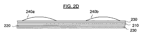
図2Dに示すように、方法は、絶縁層230にデバイス層(例えば、半導体層)240を形成する段階を更に含む。基板210上のデバイスが、CMOSトランジスタを含む(すなわち、少なくとも1つのNMOSトランジスタと少なくとも1つのPMOSトランジスタとを含む)場合、デバイス層240は、1以上の第1トランジスタ島状領域240a、及び、1以上の第2トランジスタ島状領域240bを有してもよい。第1トランジスタ島状領域240aは、第1導電型(例えば、NMOS又はPMOSの一方)の半導体材料からなり、第2トランジスタ島状領域240bは、同じ又は異なる半導体材料からなるが、第2導電型(例えば、NMOS又はPMOSの他方)を有する材料から形成されている。これに替えて、デバイス層240は、1以上のゲート電極(すなわち、ボトムゲート構造)を含んでもよく、第1ゲート電極240aは、第1の組成(例えば、第1導電型を有する第1半導体材料)又は特性の第1セット(例えば、寸法の第1パターン又は第1セットを有する金属)を有し、第2ゲート電極240bは、第2の組成(例えば、第2導電型を有する第2半導体材料)又は特性の第2セット(例えば、寸法の第2パターン又は第2セットを有する金属)を有してもよい。更なる実施形態において、デバイス層240は、1以上のキャパシタのプレート、1以上のダイオード層、1以上の抵抗器、又は配線等を含んでもよい。
As shown in FIG. 2D, the method further includes forming a device layer (eg, semiconductor layer) 240 on the insulating
ある実施形態では、デバイス層240は、シリコン及び/又はゲルマニウムを含む。しかしながら、デバイス層240が、半導体材料を含む場合、デバイス層240は、シリコン及び/又はゲルマニウムに限定されず、III−V型半導体(例えば、GaAs、InP、及び関連する化合物及び/又は合金)、II−VI型半導体(例えば、ZnO、ZnS、ZnS、ZnSe、CdTe、及び関連する化合物及び/又は合金)、有機半導体(例えば、ポリ[チアフルバレン系半導体])、又は、本発明の方法に適合するその他の好適な半導体材料により形成されていてもよい。ある実施形態では、デバイス層240は、非晶質、微結晶及び/又は多結晶のシリコン、ゲルマニウム、又は、シリコンゲルマニウムを含んでもよい。デバイス層240がシリコンゲルマニウムを含む場合、シリコンのゲルマニウムに対する比率は、約10,000:1から約1:1(又は、上記範囲内のその他の値の範囲)であってもよい。デバイス層240は更に、B、P、As又はSbのようなドーパントを含んでもよい。一実施形態において、デバイス層240は、ボロン又はリンでドープされたポリシリコンを含む。別の実施形態では、デバイス層240は、リンでドープされた第1ポリシリコン島状領域240a、及び、ボロンでドープされた第2ポリシリコン島状領域240bを含む。
In certain embodiments, device layer 240 includes silicon and / or germanium. However, if the device layer 240 includes a semiconductor material, the device layer 240 is not limited to silicon and / or germanium, and a III-V type semiconductor (eg, GaAs, InP, and related compounds and / or alloys), II-VI type semiconductors (eg ZnO, ZnS, ZnS, ZnSe, CdTe and related compounds and / or alloys), organic semiconductors (eg poly [thiafulvalene-based semiconductors]) or compatible with the method of the invention It may be formed of other suitable semiconductor materials. In some embodiments, device layer 240 may include amorphous, microcrystalline, and / or polycrystalline silicon, germanium, or silicon germanium. If device layer 240 includes silicon germanium, the ratio of silicon to germanium may be from about 10,000: 1 to about 1: 1 (or other value range within the above range). The device layer 240 may further include a dopant such as B, P, As, or Sb. In one embodiment, the device layer 240 comprises polysilicon doped with boron or phosphorous. In another embodiment, device layer 240 includes a first
ある実施形態では、デバイス層240は、(本明細書に記載したような)印刷によって形成されてもよい。例えば、ドープされていない及び/又はドープされたポリシラン、ヘテロシクロシラン、及び/又はドープされていない及び/又はドープされた半導体ナノ粒子、を含むドープされていない及び/又はドープされた半導体前躯体インクを、好適な印刷方法(例えば、インクジェット印刷、オフセットリソグラフィー、スクリーン印刷等)を使用して、所望のパターンに絶縁層230上に堆積又は印刷してもよく、その後で、デバイス層240を形成するべく硬化及び/又はアニールしてもよい。ポリシランを含む半導体前駆体インクについては、米国特許第7422708、7553545、7498015及び7485691号明細書、2007年10月4日出願の米国特許出願公開第11/867587号明細書(代理人整理番号IDR0884)に記載されており、各明細書の関連する記載部分が、参照により本明細書に組み込まれる。ヘテロシクロシランを含む半導体前躯体のインクについては、米国特許第7314513号明細書、2004年9月24日出願の米国特許出願公開10/950373号明細書(代理人整理番号IDR0301)及び2004年10月1日出願の米国特許出願公開第10/956714号明細書(代理人整理番号IDR0303)に記載されており、各明細書の関連する記載部分が、参照により本明細書に組み込まれる。ドープされたポリシランを含む半導体前躯体のインクについては、2007年10月4日出願の米国特許出願公開第11/867587号明細書(代理人整理番号IDR0884)に記載されており、明細書の関連する記載部分が、参照により本明細書に組み込まれる。ドープされていない及び/又はドープされた半導体ナノ粒子を含む半導体前躯体のインクについては、米国特許第7422708及び7553545号明細書に記載されており、各明細書の関連する記載部分が、参照により本明細書に組み込まれる。または、デバイス層240を、1以上の従来の薄膜プロセス又は技術によって形成することもできる。
In certain embodiments, device layer 240 may be formed by printing (as described herein). Undoped and / or doped semiconductor precursors comprising, for example, undoped and / or doped polysilanes, heterocyclosilanes, and / or undoped and / or doped semiconductor nanoparticles Ink may be deposited or printed on the insulating
図2Eには、本発明の方法に従って形成された半導体デバイスの例である、薄膜トランジスタ(TFT)245a−bが示されている。TFT245a−bはそれぞれ、通常、半導体層(例えば、トランジスタチャネル242a−b、第1ソース/ドレイン端子244a−b、及び第2ソース/ドレイン端子246a−bを含む)、少なくとも半導体層の一部の上に設けられるゲート絶縁層250a−b、ゲート絶縁層250a−b上に設けられるゲート金属層260a−b、半導体層及びゲート金属層260a−bに設けられる1以上の誘電体層、及び、ゲート金属層260a−b及びソース/ドレイン端子244a−b、246a−bと電気的に接続される複数の金属導体(図示せず))を含む。TFTに好適な半導体、誘電体及び金属の層の例、及びTFTを形成する材料及び方法については、米国特許第7619248号明細書、出願日がそれぞれ2005年8月11日、2005年10月3日、2006年6月12日、2007年8月3日、2007年8月3日、2007年6月12日、2007年8月21日、2008年7月17日、2008年5月2日、2008年5月30日、2008年10月1日である、米国特許出願公開第11/203563、11/243460、11/452108、11/888949、11/888942、11/818078、11/842884、12/175450、12/114741、12/131002及び12/243880号明細書(代理人整理番号IDR0213、IDR0272、IDR0502、IDR0742、IDR0743、IDR0813、IDR0982、IDR1052、IDR1102、IDR1263、IDR1574)に記載されており、各明細書の関連する記載部分が、参照により本明細書に組み込まれる。
FIG. 2E shows a thin film transistor (TFT) 245a-b, which is an example of a semiconductor device formed according to the method of the present invention. Each
TFT245a−bには、ゲート誘電体250a−bが半導体島状領域240a−bに形成される。ある実施形態では、ゲート誘電体250a−bは、印刷プロセス(例えば、ヒドロシロキサン又はヒドロケイ酸のような、二酸化シリコンの前躯体を印刷する、例えば、米国特許第7709307号明細書、2009年11月24日出願の米国特許出願公開第12/625492号明細書(代理人整理番号IDR0872に記載されており、各明細書の関連する記載部分が、参照により本明細書に組み込まれる)によって形成されていてもよい。ゲート誘電体250a−bは、溶媒又は誘電体前躯体が可溶な溶媒の混合溶液中の分子、有機金属、ポリマー及び/又はナノ粒子の前躯体のような好適な誘電体前躯体を印刷することによって、形成されてもよい。これに替えて、ゲート誘電体250は、半導体層240を全体に堆積させる(例えば、CVD又はPVDによって)及び/又は半導体層240を熱酸化することによって、形成されてもよい。例えば、ゲート誘電体250a−bは、従来の方法によって形成されてもよい(例えば、酸化シリコンの化学的気相成長法、又は酸化膜を形成するべく半導体島状領域240a−bの表面の酸化によって、酸化膜を形成する)。半導体層240が、第1導電型を有する第1ドーパント(例えば、リン)でドープされた第1ポリシリコン島状領域240a、及び第2導電型を有する第2ドーパント(例えば、ボロン)でドープされた第2ポリシリコン島状領域240bを含む場合、異なってドープされている半導体島状領域の異なる酸化率により、ゲート誘電体層250aは、ゲート誘電体層250bとは僅かに異なる厚みを有していてもよい。
In the
そして、ゲート電極260a−bがゲート誘電体250a−b上に形成されてもよい。ゲート電極260a−bは、第4、5、6、7、8、9、10、11又は12族の金属又は半導体材料(例えば、シリコン、ゲルマニウム等)を、従来の堆積方法(例えば、化学的気相成長法、物理的気相成長法、スパッタリング、原子層成長法等)によってゲート誘電体層250a−b上に堆積させることによって形成されてもよく、その後にフォトリソグラフィが行われる。ある実施形態では、ゲート電極260を形成する段階は、金属前躯体を含むインク成分を印刷又はコーティングする工程を含み、金属前躯体は、金属前躯体をコーティング又は印刷するのに適した溶媒又は溶媒混合液中の1以上の第4,5,6,7,8,9,10, 11又は12族の金属塩、金属錯体、金属クラスター、及び/又はナノ粒子を含む。ある実施形態では、金属前駆体は、金属塩、化合物及び/又は錯体を含み、これらは、金属塩、化合物及び/又は錯体の元素金属及び/又は合金への還元の際に気体又は揮発性の副産物を生成する1以上の配位子結合を有する。金属前駆体は更に、金属塩、化合物及び/又は錯体の元素金属及び/又は合金への還元の際に気体又は揮発性の副産物を生成することができる1以上の添加物(例えば、1以上の還元剤)を含んでもよい。このような金属処方により、金属前躯体及び還元剤を使用して純粋な金属を印刷することができ、前躯体及び還元剤は通常、膜中に影響が出る程度の不純物及び/又は残留物を残すことがない。更なる詳細については、2008年5月30日出願の米国特許出願公開第12/131002号明細書(代理人整理番号IDR1263)に記載されており、明細書の関連する記載部分が、参照により本明細書に組み込まれる。インク組成物のコーティング又は印刷に続いて更に、フォトリソグラフィによって金属前駆体をパターニングしてもよい。
A
続いて、半導体層240に、ソース及びドレイン領域244a−b、246a−bを、数多く存在する方法のうちのいずれかによって形成してもよい。(例えば、イオン注入、イオンシャワー、ガス浸漬レーザー堆積(GILD)、半導体層240及びゲート260上に高濃度ドープ半導体層を印刷又は堆積した後、硬化及び/又は活性化工程を行う、若しくは、1以上のドーパント層(例えば、相補的なドーパントをそれぞれ含む2つの異なる層である層270a及び270b)を、半導体層240及びゲート260に印刷又は堆積させて、その後にドライブイン工程を実行する、詳細には、米国特許第7619248及び7701011号明細書、及び出願日2007年8月3日出願の米国特許出願公開第11/888942号明細書(代理人整理番号IDR0742)に記載されており、明細書の関連する記載部分が、参照により本明細書に組み込まれる。)ソース領域244a−b及びドレイン領域246a−bを形成した後、チャネル領域242a−bがゲート電極260a−bの下に残る。
Subsequently, source and
ソース及びドレイン領域244a−b及び246a−bを形成する前又は形成した後に、ゲート260a−bから露出した(すなわち、ゲートによって覆われていない)領域のゲート誘電体層250a−bを、選択的ウェットエッチング又はドライエッチングにより取り除いてもよい。ソース及びドレイン領域244a−b及び246a−bが、半導体層240及びゲート260上にドーパント層を印刷又は堆積し、その後にドライブイン及び/又は活性化工程を実行して形成される場合、更なる処理(必要に応じて、露出したゲート誘電体層を取り除く前)を行う前に、通常は、ドーパント層が取り除かれる。
Before or after forming the source and
1以上の誘電体層270(例えば、第1及び第2層間誘電体270a及び270b)が次いでゲート260a−b、ソース及びドレイン領域244a−b及び246a−bの上に、多くの場合、全面堆積又は印刷(本明細書に記載されるように)によって堆積される。ある実施形態では、誘電体層は、1以上の誘電体前躯体及び1以上の溶媒を含むインクを印刷することによって形成される。通常、誘電体前躯体は、二酸化シリコン、窒化シリコン、酸化窒化シリコン、アルミン酸塩、チタン酸塩、チタンケイ酸塩、ジルコニア(酸化ジルコニウム)、ハフニア(酸化ハフニウム)、又はセリア(酸化セリウム)を含む。別の実施形態では、誘電体前躯体は、有機ポリマー又は有機ポリマーの前躯体(例えば、アクリル酸、メタアクリル酸、及び/又はアクリル酸のエステル、及び/又はメタアクリル酸のポリマー又は共重合体)である。印刷の後、誘電体のインクを乾燥及び硬化させる。印刷されたインクの乾燥は、真空下又は不活性雰囲気又は酸化雰囲気下で、50℃から150℃の温度で、印刷されたインクから実質的に全ての溶媒を取り除くのに十分な時間、加熱することを含んでもよい。乾燥された誘電体前駆体の硬化は、不活性雰囲気又は酸化雰囲気下で、例えば、200℃から500℃の温度(又は、この範囲内のあらゆる値の範囲)で、前駆体を所望の誘電体材料へと変換させるのに十分な時間、加熱することを含んでもよい。
One or more dielectric layers 270 (eg, first and
さらに、誘電体270a−bにコンタクトホール(図示せず)を設けてもよく、1以上の更なるデバイス(例えば、TFT245の)ゲート260a/b、ソース/ドレイン端子244a/b及び246a/bに接続するための金属線及び/又は配線(図示せず)を形成してもよい。これに替えて、誘電体層270a−bが、印刷によって形成される場合、印刷されたパターンは、ゲート260a−b及びソース/ドレイン端子244a−b及び246a−bそれぞれの表面を露出させる複数のコンタクトホールを含んでもよい。一実施形態では、金属線/配線は、印刷によって形成される。(出願日2008年7月17日出願の米国特許出願公開第12/175450号明細書(代理人整理番号IDR1052)、出願日2008年5月30日出願の米国特許出願公開第12/131002号明細書(代理人整理番号IDR1263)参照、明細書の関連する記載部分が、参照により本明細書に組み込まれる。)一例では、導電材料シード層が、金属線及び/又は配線のパターンに印刷され、バルク金属又は金属合金が(例えば、電気めっき又は無電解めっきにより)パターン上にめっきされる。これに替えて、金属線及び/又は配線を、従来の薄膜及び/又は堆積及びフォトリソグラフィ工程によって形成してもよい。
In addition, contact holes (not shown) may be provided in the
TFT245は、NMOSトランジスタ又はPMOSトランジスタであり、トランジスタ、ダイオード、抵抗器、キャパシタ、又はオフ状態で接続されるTFTとして機能するよう構成される及び/又は電気的に接続されていてもよい。図2Eには、ドーム型の形状を有するTFT245が例示されている。(例えば、出願日2008年10月1日出願の米国特許出願公開第12/243880号明細書(代理人整理番号IDR1574)参照、明細書の関連する記載部分が、参照により本明細書に組み込まれる。)通常、半導体島状領域(例えば、図2Dの240a及び/又は240b)、及びゲート(例えば、図2Eの260a及び/又は260b)は、印刷で形成される場合に、ドーム形状を有していてもよい。TFT245のようなTFTを形成するための"全印刷"による方法における各製造工程は、様々に変更可能であり、それに伴ってTFT245の寸法、境界及び表面も変化してもよい。したがって、印刷される構造の断面及び/又は(上から見た)レイアウト形状及び/又は外形は、構造によって変化してもよい。 The TFT 245 is an NMOS transistor or a PMOS transistor, and may be configured and / or electrically connected to function as a transistor, a diode, a resistor, a capacitor, or a TFT connected in an off state. FIG. 2E illustrates a TFT 245 having a dome shape. (See, eg, US Patent Application Publication No. 12/243880 (Attorney Docket No. IDR1574) filed on Oct. 1, 2008, the relevant description of which is incorporated herein by reference. .) Typically, semiconductor island regions (eg, 240a and / or 240b in FIG. 2D) and gates (eg, 260a and / or 260b in FIG. 2E) have a dome shape when formed by printing. It may be. Each manufacturing process in the “full printing” method for forming a TFT such as the TFT 245 can be variously changed, and the dimensions, boundaries, and surface of the TFT 245 may be changed accordingly. Accordingly, the cross-section and / or layout shape and / or outline (viewed from above) of the printed structure may vary from structure to structure.
したがって、一実施形態では、TFT245は、"全印刷"プロセスによって形成されてもよい。TFT245の1以上の層を印刷によって形成する実施形態の場合には、印刷された前躯体のインクは、通常、乾燥及び硬化される。インクを乾燥させて、乾燥させた前駆体を硬化させる時間の長さ及び温度は、インクの処方及び含まれている前躯体によって異なるが、多くの場合、インクは、印刷されたインクから溶媒が実質的に全て取り除かれるのに十分な時間の長さ及び温度で乾燥され、乾燥された前駆体に対して、前躯体を最終的な膜の材質(例えば、半導体、誘電体又は金属)に変換するのに十分な時間の長さ及び温度で、硬化が行われる。印刷されたTFTの例に関する更なる説明、及びこのような印刷されたTFTを形成する方法については、出願日2007年5月23日出願の米国特許出願公開第11/805620号明細書(代理人整理番号IDR0712)及び出願日2008年10月1日出願の米国特許出願公開第12/243880号明細書(代理人整理番号IDR1574)に記載されており、明細書の関連する記載部分が、参照により本明細書に組み込まれる。これに替えて、TFT245を、印刷及び従来の製造工程との混合、又は従来の製造技術のみ(例えば、薄膜技術)のみを使用して、形成してもよい。 Thus, in one embodiment, TFT 245 may be formed by a “full print” process. In embodiments where one or more layers of TFT 245 are formed by printing, the printed precursor ink is typically dried and cured. The length of time and temperature at which the ink is dried and the dried precursor is cured will vary depending on the ink formulation and the precursor contained, but in many cases, the ink will have a solvent from the printed ink. For a precursor that has been dried for a length of time and at a temperature sufficient to remove substantially all of the precursor, convert the precursor to the final film material (eg, semiconductor, dielectric or metal). Curing is carried out for a sufficient length of time and temperature to do. For further description of printed TFT examples and methods of forming such printed TFTs, see US Patent Application Publication No. 11/805620, filed May 23, 2007 (Attorney). No. IDR0712) and US Patent Application Publication No. 12/243880 (Attorney Docket No. IDR1574) filed on Oct. 1, 2008, the relevant description part of which is incorporated by reference Incorporated herein. Alternatively, the TFT 245 may be formed using printing and mixing with conventional manufacturing processes, or using only conventional manufacturing techniques (eg, thin film technology).
上述したように、"ボトムゲート"型デバイスを、コーティングした基板上に形成することができる。ゲート電極240a−b(図2D)を形成した後、ゲート誘電層を、図2Eの層250a−bを参照して説明した1以上の方法によってゲート電極の上に形成することができる。トランジスタ本体(図2Eの層260a−bに類似)を、ゲート誘電体層の上に形成することができ、周知の工程によってドープすることができる。(出願日2005年10月3日出願の米国特許出願公開第11/243460号明細書(代理人整理番号IDR0272)及び出願日2008年4月24日出願の米国特許出願公開第12/109338号明細書(代理人整理番号IDR1322)参照、明細書の関連する記載部分が、参照により本明細書に組み込まれる。)図2Eにおける層270a−bと同様なバルク誘電体層を、本明細書に開示するような態様で形成及び/又はパターンニングすることができ、また、上述したように、コンタクトホールを形成し、下に配置されるデバイス層(例えば、トランジスタ本体のゲート電極及びソース/ドレイン端子)と接触して配線を形成することができる。
As described above, “bottom gate” type devices can be formed on a coated substrate. After forming the
更なる別の実施形態において、拡散バリア層でコーティングされた金属基板上のデバイスは、1以上のキャパシタ、ダイオード、抵抗器及び配線を含むことができる。キャパシタは、通常、第1及び第2キャパシタプレート、及び、第1及び第2キャパシタプレートの間に誘電体材料を含む。ダイオードは、通常、異なるドーピング型及びドーピング量を持つ導電体又は半導体材料の複数の(例えば、2から5層)ダイオード層を含む。例えば、2層のダイオードでは、第1層はP型の半導体を含む又は主にP型の半導体によって構成され、第2層はN型の半導体を含む又は主にN型の半導体によって構成されてもよい。3層のダイオードでは、第1層が高濃度にドープされたP型の半導体を含む又は主に高濃度にドープされたP型の半導体によって構成され、第2層が真性の半導体、又は低濃度にドープされたP型又はN型半導体を含む又はこれらによって主に構成され、第3層が、高濃度にドープされたN型の半導体を含む又は主に高濃度にドープされたN型の半導体によって構成されていてもよい。例示されたダイオードでは、上記のP型又はN型の半導体層は、異なるドーピング濃度を有する複数の副層を含む又は複数の副層によって主に構成されてもよい(例えば、1以上の高濃度ドープ層又は非常に高濃度にドープされた層、及び1以上の低濃度ドープ層又は非常に低濃度にドープされた層)。抵抗及び/又は配線は、通常は、あるパターンに、コーティングされた基板及び/又はデバイス層上に形成される。キャパシタプレート、抵抗器及び/又は配線は、本明細書に開示したような半導体及び/又は導電体材料を含んでもよく、ダイオード層は通常、本明細書に開示したような半導体材料を含む。キャパシタプレート、ダイオード層、抵抗器及び/又は配線は、本明細書に開示した、いかなる工程によって形成されてもよい。 In yet another embodiment, a device on a metal substrate coated with a diffusion barrier layer can include one or more capacitors, diodes, resistors, and wiring. The capacitor typically includes a dielectric material between the first and second capacitor plates and the first and second capacitor plates. The diode typically includes multiple (eg, 2 to 5) diode layers of conductor or semiconductor material having different doping types and amounts. For example, in a two-layer diode, the first layer includes a P-type semiconductor or is mainly composed of a P-type semiconductor, and the second layer includes an N-type semiconductor or is mainly composed of an N-type semiconductor. Also good. In the three-layer diode, the first layer includes a heavily doped P-type semiconductor or is mainly composed of a heavily doped P-type semiconductor, and the second layer is an intrinsic semiconductor or a lightly doped semiconductor. A third layer comprising or mainly heavily doped N-type semiconductor comprising or mainly composed of P-type or N-type semiconductor doped with It may be constituted by. In the illustrated diode, the P-type or N-type semiconductor layer may include a plurality of sublayers having different doping concentrations or may be mainly constituted by a plurality of sublayers (for example, one or more high concentrations). Doped layers or very heavily doped layers and one or more lightly doped layers or very lightly doped layers). Resistors and / or wires are typically formed on a coated substrate and / or device layer in a pattern. Capacitor plates, resistors and / or wires may include semiconductor and / or conductor materials as disclosed herein, and diode layers typically include semiconductor materials as disclosed herein. The capacitor plate, diode layer, resistor, and / or wiring may be formed by any process disclosed herein.
別の実施形態では、図3A〜3Cに示すように、金属基板310は、金属基板310(図3B参照)の一主面に、上記したような1以上の工程によって堆積された拡散バリア層320を有してもよい。更なる実施形態(図示せず)では、金属基板310の少なくとも1つ(且つ全部ではない)の面は、拡散バリア層320によって被覆されていてもよい。例えば、金属基板310が形成される前のロール状態又はシート状態のものを加工する場合には、金属基板310の対向する面を拡散バリア層320で覆い(例えば、半導体構造又はデバイスが後に形成される予定の金属基板310の主面)、金属基板310の1以上の側縁は覆わないようにしてもよい。これに替えて、洗浄工程の前又は後に、金属基板310を形成又は切り出して、金属基板310の1つの主面と縁部とを被覆するように拡散バリア層320を形成してもよい。
In another embodiment, as shown in FIGS. 3A-3C, the
図3Cに示すように、拡散バリア層320が、金属基板310の1つの主面に堆積される実施形態では、金属基板310の拡散バリア層320が被覆されている部分を覆うように、本明細書に記載したような1以上の工程により、絶縁層330を堆積させてもよい。金属基板310の少なくとも1つの面であって全部の面ではない面が、拡散バリア層320で被覆される更なる実施形態(図示せず)の場合、この拡散バリア層320で被覆される領域が、続いて、絶縁層330で覆われてもよい(例えば、金属基板310の上面及び側面が拡散バリア層320及び絶縁層330によって被覆されていてもよい)。
As shown in FIG. 3C, in an embodiment in which the
[反射防止特性を有するバリア層が被覆される金属基板の例]
金属箔基板を使用する際に問題となるのが、金属基板及び/又はバリア層(図4A−4B参照)の相対的に高い反射率である。組成物膜の積層体(例えば、金属箔410、1以上の拡散バリア材420/425及び1以上の絶縁層430を典型的には含む金属−バリア−絶縁体の積層体)の光学定数及び厚みは、デバイスを製造する際に使用される光の波長に応じて、様々な程度で光を吸収及び反射するのに関係し、少なくとも、入射光の角度に関係する。
[Example of metal substrate coated with a barrier layer having antireflection properties]
A problem in using a metal foil substrate is the relatively high reflectance of the metal substrate and / or the barrier layer (see FIGS. 4A-4B). Optical constants and thicknesses of a laminate of composition films (eg, a metal-barrier-insulator laminate typically comprising a
具体的には、金属−バリア−絶縁体の積層体に堆積されたシリコン又はその他の電気デバイス層440を結晶化させるのに可視光の波長域(例えば、レーザー及び/又は閃光電球のようなその他の高輝度光源)を使用すると、大部分の光をシリコン膜440を通過させることができる。シリコン膜440を通過する光は、少なくとも一部、金属箔410及び/又はバリア層(例えば、図4Aにおける420)で反射される。シリコン膜440の膜厚、及び金属−バリア−絶縁体の積層体を構成する層の膜厚が最適化されていない及び/又は不均一であること、及び、光との相互作用に対して相対的に高い感度を有する(例えば、光の直接吸収及び/又は下に位置する層で反射されてきた光の吸収)ことから、シリコン膜440の光吸収は変化する場合がある。このようなシリコン膜440の光との相互作用に対する感度により、結晶性の均一性及び粒状構造が大きく変化する場合があり、(例えば、同じ処理ロット内で)異なる基板と所与の基板との間で、望ましくないデバイスばらつきの発生につながっている。特に、窒化アルミニウム(良質な拡散バリアである)と、可視光の波長域(例えば、緑色の波長域)で光を発するレーザーとを組み合わせて使用する場合に、シリコン結晶化に大きな影響を及ぼす。
Specifically, the wavelength range of visible light (such as lasers and / or other flash bulbs, etc.) is used to crystallize silicon or other
シリコン膜における光との相互作用に対する相対的に高い感度によって生じている、光吸収の変動の効果を低減する、最小化する又は取り除くために、1以上の反射防止層(例えば、図4Bの層425)を、金属−バリア−絶縁体の積層体の一部として、第1バリア層420上に形成してもよい。これに替えて、反射防止層425を、金属基板410又は絶縁層430上に形成してもよい。反射防止層425の材料は、シリコン結晶化に使用される光の波長において、その反射率が低くなるように選択されてもよい。これに替えて、反射防止層425の材料は、太陽電池(PVセル)に有用な波長において反射率が低くなるように選択されてもよい。反射防止層425は、拡散バリア420の一部として(例えば、バリア層/反射防止層の二層420/425)堆積されてもよく、反射防止層の利用を高めることができ、結晶化のプロセスウィンドーを広げ、デバイスの歩留まり及び/又は性能を向上させることができる。理想的には(必ずしもそうでなくてもよいが)、反射防止層425は、バリア層420及び/又は絶縁膜430を形成するのと同一の膜成長の装置(例えば、原子層成長装置、統合CVDスパッタクラスタ装置、スピンオングラス及び硬化装置、等)を使用して、一続きの工程で堆積される。
One or more anti-reflective layers (eg, the layer of FIG. 4B) to reduce, minimize or eliminate the effects of light absorption variations caused by the relatively high sensitivity to interaction with light in the silicon film. 425) may be formed on the
1つの層が、反射防止機能及び拡散バリア機能(例えば、下に位置する金属基板410からの不純物の外方向への拡散を防ぐバリアとして機能する)の両方を有すれば有益であるが、本発明にこの構成が必須であるということではない。すなわち、金属−バリア−絶縁体の積層体におけるバリア層は、(i)拡散バリア特性のみを有する1以上の層及び反射防止特性を有する少なくとも1つの層、(ii)反射防止特性のみを有する1以上の層及び拡散バリア特性のみを有する少なくとも1つの層、(iii)拡散バリア特性及び反射特性の両方を有する1以上の層、又は(iv)これらの組み合わせを含む。反射防止コーティング(ARC)層は、その層に対する所望の光学特性に依存して、同時に、絶縁性を有する場合がある(例えば、酸化窒化シリコン(ここで、Si:O:Nの比は、選択可能である)、TiO2、アルミナ、ZrO2及び/又はその他の酸化金属のような誘電率kが高い膜)。 It would be beneficial if one layer had both an anti-reflective function and a diffusion barrier function (eg, functioning as a barrier to prevent outward diffusion of impurities from the underlying metal substrate 410) This configuration is not essential to the invention. That is, the barrier layer in the metal-barrier-insulator stack includes (i) one or more layers having only diffusion barrier properties and at least one layer having antireflection properties, and (ii) 1 having only antireflection properties. And at least one layer having only the above layers and diffusion barrier properties, (iii) one or more layers having both diffusion barrier properties and reflection properties, or (iv) a combination thereof. An anti-reflective coating (ARC) layer may be insulating at the same time, depending on the desired optical properties for the layer (eg, silicon oxynitride (where the Si: O: N ratio is selected) Possible), films with a high dielectric constant k, such as TiO 2 , alumina, ZrO 2 and / or other metal oxides).
具体的には、窒化チタン(又は、例えば、酸化窒化シリコン)を、それのみで反射防止膜425として使用することができ、又は、窒化アルミニウム膜420と組み合わせて反射防止膜としてもよい。膜を、2重層のバリア積層体として堆積させてもよい(例えば、金属基板410−AlN 420−TiN 425−絶縁層430で構成される積層体、又は、金属基板−TiN−AlN−絶縁層で構成される積層体)、又は、交互に積層されたナノ積層体の態様(例えば、金属基板−ナノ積層体−絶縁層で構成される積層体、ここで、ナノ積層体の各層は、1以上のAlNの単層及び1以上のTiNの単層を含み、ナノ積層体の層の数は、1から10,000のいずれかであってもよい)であってもよい。バリア及び反射防止膜として使用するナノ積層体の効率を最大にする厚みを、経験的に決定してもよい。ナノ積層体の典型的な厚みは、1−100nm(又は、上記範囲に含まれるあらゆる値の範囲)である。図5に示すように、TiN−AlNナノ積層体を使用することにより、反射率を75%低減することができ、純粋なAlNだけ(又は同様な材料)の場合と比較して、レーザー結晶化の間の光結合及び積層体の感度を低減することができる。また、光結合及び積層体の感度が低減されたことから、シリコン膜をより均一に結晶化することができ及び/又はその他にもシリコン膜の品質を高めることができる。
Specifically, titanium nitride (or silicon oxynitride, for example) alone can be used as the
シリコン又はその他のデバイス層の結晶化のための光源の可視光波長(例えば、緑)で使用される(例えば、窒化チタンのような)反射防止材料の使用は、光(又は光源)のあらゆる波長域に対して特別に波長調整されてもよい。波長調整には、デバイスの集積構造全体内に適合する所望の反射防止特性を有する好適な材料を使用することも含まれる。 The use of an antireflective material (such as titanium nitride) used at the visible light wavelength (eg, green) of the light source for crystallization of silicon or other device layers will allow any wavelength of light (or light source). The wavelength may be specially adjusted with respect to the area. Wavelength tuning also includes the use of suitable materials having the desired anti-reflective properties that fit within the overall integrated structure of the device.
[応力緩和特性を有するバリアが被覆された金属基板の例]
金属箔の基板を使用した場合に生じ得るもう1つの問題として、多くの場合、応力によって発生する金属基板における粒状の高輝度領域が挙げられる。粒状の高輝度領域は、次に行われる処理工程に影響を与える場合がある。バリア材料の中には、高い固有応力を有するものが存在し、バリア層の積層体及び/又は組成を、この固有応力を考慮に入れて最適化してもよい。
[Example of metal substrate coated with a barrier having stress relaxation properties]
Another problem that can arise when using a metal foil substrate is often the granular high-brightness region of the metal substrate that is generated by stress. The granular high-intensity region may affect the next processing step. Some barrier materials have high intrinsic stress, and the laminate and / or composition of the barrier layer may be optimized taking this intrinsic stress into account.
金属箔を含む基板(例えば、図2Aにおける基板210)を効率的にパッシベーションし、(外部拡散を介した)直接的な汚染又は(例えば、処理装置、溶液層等との封止されていない金属箔基板210との接触による)間接的な汚染を防ぐためには、拡散バリア(例えば、図2Aにおける層220)は、基板の側縁を含む基板210の露出した面全てを封止する必要がある。拡散バリア220の寸法、組成、及び/又は物理的、化学的及び/又は機械的特性を最適化して、金属基板210及び/又は1以上のバリア層(例えば、図4A−4Bにおける420及び/又は425)の光学的反射性に起因する製造工程で発生する問題の程度を低減することができる。
Efficiently passivate a substrate containing a metal foil (eg,
金属拡散バリアとしての窒化チタン膜(例えば、図2Aの層220)を、ステンレス鋼210に直接堆積させて、基板210の全ての面及び側縁を完全に封止させてもよい。ある実施形態(例えば、バリア膜をALDによって堆積する場合)では、プロセスの条件に応じて、バリア層220を堆積する前に、接着層を基板210上に形成してもよい。その後に、同様な態様で、絶縁層230(例えば、公称厚みが1ミクロンである二酸化シリコン層)による封止を行ってもよい。基板210の洗浄(例えば、残留物、有機物、粒子等の除去)を、バリア層220の堆積の前に行うことが望ましく、洗浄を行うことにより、高温におけるバリア層220の密着性を良好にすることができる。高温で(例えば、数時間単位の時間、850℃で複数回熱サイクルで試験したところ)、TiNバリア220は、効果的に、鉄及びクロム(鋼基板210の主要で最も速く拡散する成分)がSiO2の絶縁層230の表面に形成された能動シリコンTFTデバイスへと拡散するのを防止する(例えば、図5参照)。また、ニッケル、及びCo、Mo、Ti、Nb等のステンレス鋼中のその他の合金の成分が、絶縁層230の表面(及び、その上に形成されているデバイス層)へと拡散するのも防止される。
A titanium nitride film as a metal diffusion barrier (eg,
一実施形態において、バリア層は、接着層として機能するAlNの第1層、応力緩和層として機能するSiO2:Alの層、及び拡散バリアとして機能するAlNの層を含む。典型的なAlNの第1層は、10−100Åの厚さを有するが、10−5000Åの範囲であれば、いかなる厚さであってもよい。応力緩和層(例えば、SiO2:Al)は、10−500Åの厚さを有してもよく、10−5000Åの範囲であれば、いかなる厚さであってもよい。好ましくは、応力緩和層は、ALDによって堆積される。典型的なAlNの第2の層は、200−2000Åの厚さを有するが、50−10,000Åの範囲であれば、いかなる厚さであってもよい。この段落において引用される接着層及び応力緩和層の代替構成としては、Al2O3、窒化シリコン、酸化窒化シリコン、酸化シリコン、酸化チタン、及び、ジルコニウム、ハフニウム又は希土類金属の酸化物、又は、これらの組み合わせ、又はこれらの合金であって、上記した厚みと同様な厚みの範囲で形成されたものを含む。材料及び寸法の選択は、所望の材料の特性及び製造工程統合スキーム全体への適合性に依存して行ってもよい。 In one embodiment, the barrier layer includes a first layer of AlN that functions as an adhesion layer, a layer of SiO 2 : Al that functions as a stress relaxation layer, and a layer of AlN that functions as a diffusion barrier. A typical AlN first layer has a thickness of 10-100 mm, but can be any thickness in the range of 10-5000 mm. Stress relaxation layer (e.g., SiO 2: Al) may have a thickness of 10-500A, be in the range of 10-5000A, may be of any thickness. Preferably, the stress relaxation layer is deposited by ALD. A typical AlN second layer has a thickness of 200-2000 mm, but can be any thickness in the range of 50-10,000 mm. Alternative configurations for the adhesion and stress relaxation layers cited in this paragraph include Al 2 O 3 , silicon nitride, silicon oxynitride, silicon oxide, titanium oxide, and oxides of zirconium, hafnium or rare earth metals, or These combinations, or alloys thereof, including those formed in the same thickness range as described above. The choice of materials and dimensions may be made depending on the desired material properties and suitability for the overall manufacturing process integration scheme.
上記したように、拡散バリアとして機能するその他の材料として、TiN及びTiAlNが含まれる(ここで、Alに対するTiの比は、用途に依存する、例えば、拡散バリア膜の積層体の応力及び反射性は、TiのAlに対する比を変更することによって調整可能である)。TiN及び/又はTiAlN膜は、スパッタリング(堆積の前に、鋼の表面のスパッタエッチを必要に応じて行っても、行わなくてもよい)、又は化学的気相成長法(CVD)のような様々な方法によって堆積されてもよく、原子層成長(ALD)による堆積が特に好ましい。応力緩和層及び/又は更なる拡散バリア層により、温度が最高850℃になる複数回の熱サイクルの間に、デバイス(例えば、図2EのTFT245)に対する好適な保護を提供することができる。この方法は、基板210及びバリア層220をデバイス層(例えば、図2D−2Eの240)から電気的に分離するべく、絶縁膜(例えば、SiO2及び/又はAl2O3)と組み合わせることができ、好ましくは、同じ堆積装置(又は、別の堆積工程で)で絶縁膜で被覆する。
As described above, other materials that function as diffusion barriers include TiN and TiAlN (where the ratio of Ti to Al depends on the application, for example, stress and reflectivity of the stack of diffusion barrier films). Can be adjusted by changing the ratio of Ti to Al). TiN and / or TiAlN films can be sputtered (sputter etch of the steel surface may or may not be performed as needed prior to deposition), or chemical vapor deposition (CVD). It may be deposited by various methods, with atomic layer deposition (ALD) deposition being particularly preferred. The stress relaxation layer and / or additional diffusion barrier layer can provide suitable protection for the device (eg, TFT 245 of FIG. 2E) during multiple thermal cycles where the temperature is up to 850 ° C. This method combines an insulating film (eg, SiO 2 and / or Al 2 O 3 ) to electrically isolate the
拡散バリア層は、1以上の処理問題を解決してもよい。例えば、窒化金属膜(又は、これに替えて、金属炭化物、窒化シリコン又は炭化シリコン膜)は大きな応力を有する、又はデバイスにおけるその他の層に大きな応力を加えることがある。この応力によって、膜の剥離、又は、下に位置する鋼基板の変形につながる可能性がある。膜の積層体に1以上の更なる材料を含ませることにより、この応力を大幅に低減させることができる。例えば、窒化金属の下に酸化層を追加する、又は、TiN:AlNのような積層体を形成する(TiN:AlNは、ナノ積層体におけるTiN層のAlN層に対する比を表す)ことにより、応力を緩和できる。一例では、TiNの単層を8つ形成し、続いて、AlNの単層を3つ形成したブロック(及び、所定の全膜厚を達成するまで、この工程を繰り返す)により、応力緩和及び拡散バリア特性を提供することができ、TiNとAlNの単層を交互に配置した構成は、幾つ提供されていてもよい(例えば、TiNの単層を5−100層、AlNの単層を1−50層)。このような応力緩和の酸化層が下に形成さされていない場合には、AlN膜(例えば、図4Aの420)が、高温で基板410から剥離してしまう可能性がある。したがって、一実施形態において、ステンレス鋼基板上のTFTデバイス(例えば、図2Eの245)は、約1nmから約1000nm(例えば、一実施形態では、約100Å)の厚みを有するスパッタ形成されたTiNの層、及び、約10nmから約1500nm(例えば、一実施形態では、約300nm)の厚みを有する(上記した)ALDによって形成されたTiAlNの層を含むことができる。
The diffusion barrier layer may solve one or more processing problems. For example, a metal nitride film (or alternatively, a metal carbide, silicon nitride, or silicon carbide film) may have a high stress or may apply a high stress to other layers in the device. This stress can lead to delamination of the film or deformation of the underlying steel substrate. By including one or more additional materials in the film stack, this stress can be significantly reduced. For example, by adding an oxide layer under the metal nitride or forming a laminate such as TiN: AlN (TiN: AlN represents the ratio of TiN layer to AlN layer in the nanolaminate). Can be relaxed. In one example, eight monolayers of TiN are formed, followed by a block of three monolayers of AlN (and the process is repeated until a predetermined total film thickness is achieved), to relieve stress and diffuse. Any number of configurations in which TiN and AlN monolayers are alternately arranged may be provided (for example, 5-100 monolayers of TiN and 1-monolayers of AlN may be provided). 50 layers). If such a stress relaxation oxide layer is not formed underneath, the AlN film (eg, 420 in FIG. 4A) may peel off from the
鋼基板の粒子及び鋼基板の高い反射率によって、次の工程で行われる、光による検査又はスチール箔基板のアライメントが難しくなっていた。基板の高い反射率は、結晶化工程におけるレーザープロセスにも問題を引き起こしていた。また、基板が高い反射性を有することにより、反射されたレーザーエネルギーが入射レーザーエネルギーと干渉して、高い/低いエネルギーのノードで定常波を発生させてしまうことが原因となり、膜の積層体表面における放射線量の変動が発生する場合がある。このような効果の影響を抑制するべく、拡散バリア層の厚み及び組成を最適化して、光学的に不透明とし、下に位置する1以上の層の表面、及び/又は金属基板の表面からの反射を最小限にすることができる。 The steel substrate particles and the high reflectivity of the steel substrate make it difficult to inspect with light or align the steel foil substrate in the next step. The high reflectivity of the substrate has also caused problems in the laser process in the crystallization process. Also, the high reflectivity of the substrate causes the reflected laser energy to interfere with the incident laser energy and cause standing waves at high / low energy nodes, resulting in Variations in radiation dose may occur. In order to suppress the influence of such effects, the thickness and composition of the diffusion barrier layer are optimized to be optically opaque, and the reflection from the surface of one or more underlying layers and / or the surface of the metal substrate Can be minimized.
TiN及びその合金は相対的に安価であり、多くの場合、単層膜として形成され、様々な堆積方法(例えば、多くの実施形態で、両面堆積)に適している。TiN以外の本発明に係る拡散バリア被覆基板に使用される金属膜については、Afentakis他、IEEE Transactions on Electron Devices、vol.53、No.4(2006年4月)、p.815に記載されており、関連する記載箇所が参照により、本明細書に組み込まれる。 TiN and its alloys are relatively inexpensive, often formed as a single layer film, and are suitable for various deposition methods (eg, double-sided deposition in many embodiments). Other than TiN, the metal film used for the diffusion barrier coated substrate according to the present invention is described in Afentakis et al., IEEE Transactions on Electron Devices, vol. 53, no. 4 (April 2006), p. 815, the relevant description is hereby incorporated by reference.
[結論/まとめ]
したがって、本発明は、拡散バリア層で被覆された基板上に形成された半導体デバイスを提供する。本発明は、拡散バリア層が形成されている金属基板から金属原子が、金属基板上に形成されている半導体デバイスへと拡散するのを防ぐ。
[Conclusion / Summary]
Accordingly, the present invention provides a semiconductor device formed on a substrate coated with a diffusion barrier layer. The present invention prevents metal atoms from diffusing from a metal substrate on which a diffusion barrier layer is formed into a semiconductor device formed on the metal substrate.
上記の本発明の特定の実施形態は、例示及び説明を目的として示されている。上記の記載は、本発明を完全に説明する、又は開示された形態に厳密に限定されることを意図しておらず、数多くの変形及び変更が上記の教示することろから可能であることは明らかである。また、上記に記載した実施形態は、本発明の原理及び実用的応用を最も良く説明するために記載されており、当業者であれば本発明を良好に利用することができ、様々な変更を伴う様々な実施形態を、特定の実施に適合するように考えうる。本発明の範囲は、添付の特許請求の範囲及びその均等物によって規定される。
[項目1]
a)金属基板と、
b)上記金属基板上の1以上の拡散バリア層と、
c)上記拡散バリア層上の1以上の絶縁層と、
d)上記1以上の絶縁層上のデバイス層とを備えるデバイス。
[項目2]
上記金属基板が、上記拡散バリア層のうちの少なくとも1つ及び上記絶縁層のうちの少なくとも1つによって封止されている項目1に記載のデバイス。
[項目3]
上記金属基板の少なくとも1つの面が、上記拡散バリア層のうちの少なくとも1つ及び上記絶縁層のうちの少なくとも1つによって被覆されている項目1に記載のデバイス。
[項目4]
上記金属基板は、アルミニウム、銅、チタン、ステンレス鋼又はモリブデンを含む項目1に記載のデバイス。
[項目5]
上記金属基板は、約10μmから約1000μmの厚みを有する項目1に記載のデバイス。
[項目6]
上記拡散バリア層の少なくとも1つは、チタン化合物を含む項目1に記載のデバイス。
[項目7]
上記チタン化合物は、Ti x N y 又はTi a Al b N c を含み、ここで、x+y=1又はa+b+c=1である項目6に記載のデバイス。
[項目8]
上記1以上の拡散バリア層は、約10nmから約1μmの厚みを有する項目1に記載のデバイス。
[項目9]
上記1以上の絶縁層は、酸化シリコン、窒化シリコン、酸化窒化シリコン、酸化アルミニウム、又はこれらの組み合わせを含む項目1に記載のデバイス。
[項目10]
上記1以上の絶縁層は、約100nmから約10μmの厚みを有する項目9に記載のデバイス。
[項目11]
上記デバイス層は、半導体層を含む項目1に記載のデバイス。
[項目12]
上記半導体層は、シリコン及びゲルマニウムの少なくとも一方を含む項目11に記載のデバイス。
[項目13]
上記半導体層は、多結晶シリコン及び多結晶ゲルマニウムの少なくとも一方を含む項目12に記載のデバイス。
[項目14]
上記半導体層は、B、P、As及びSbからなる群から選択されるドーパントを更に含む項目13に記載のデバイス。
[項目15]
上記半導体層上又は下に、ゲート電極を更に備え、
上記ゲート電極は、ゲート及びゲート誘電体層を有する項目11に記載のデバイス。
[項目16]
上記半導体層は、第1導電型の第1ドーパントを有し、
上記デバイスは更に、上記半導体層の上又は上方に、第2半導体層を備え、
上記第2半導体層は、第2導電型の第2ドーパントを有する項目11に記載のデバイス。
[項目17]
上記デバイス層は、第1導電層を有し、
上記第1導電層は、第1金属層及び第1高濃度ドープ半導体層からなる群から選択される項目1に記載のデバイス。
[項目18]
上記第1導電層上の誘電体層と、
上記第1導電層上の第2導電層とを更に備え、
上記第2導電層は、第2金属層及び第2高濃度ドープ半導体層からなる群から選択される項目17に記載のデバイス。
[項目19]
上記金属基板上又は上方に、反射防止層を更に備える項目1に記載のデバイス。
[項目20]
上記デバイス層は、上記反射防止層の上方に位置する項目19に記載のデバイス。
[項目21]
上記金属基板上又は上方に、応力緩和層を更に備える項目1に記載のデバイス。
[項目22]
金属基板上にデバイスを形成する方法であって、
a)上記金属基板上に、1以上の拡散バリア層を形成する工程と、
b)上記拡散バリア層上に、1以上の絶縁層を形成する工程と、
c)上記1以上の絶縁層上に、デバイス層を形成する工程とを備えるデバイス。
[項目23]
上記金属基板が、上記拡散バリア層のうちの少なくとも1つ及び上記絶縁層のうちの少なくとも1つによって封止される項目22に記載の方法。
[項目24]
上記金属基板の少なくとも1つの面が、上記拡散バリア層のうちの少なくとも1つ及び上記絶縁層のうちの少なくとも1つによって被覆される項目22に記載の方法。
[項目25]
上記1以上の拡散バリア層を形成する前に、上記金属基板を洗浄する工程を更に備える項目22に記載の方法。
[項目26]
上記金属基板を洗浄する工程は、上記金属基板をスパッタエッチングする工程を含む項目25に記載の方法。
[項目27]
上記金属基板は、アルミニウム、銅、チタン又はステンレス鋼を含む項目22に記載の方法。
[項目28]
上記金属基板は、約10μmから約1000μmの厚みを有する項目22に記載の方法。
[項目29]
上記1以上の拡散バリア層を形成する工程は、チタン化合物の物理的気相成長、原子層成長又は化学的気相成長を含む項目22に記載の方法。
[項目30]
上記1以上の拡散バリア層を形成する工程は、原子層成長を含む項目29に記載の方法。
[項目31]
上記チタン化合物は、Ti x N y 又はTi a Al b N c を含み、ここで、x+y=1又はa+b+c=1である項目29に記載の方法。
[項目32]
上記xは約0.5であり、上記yは約0.5である項目31に記載の方法。
[項目33]
上記1以上の拡散バリア層は、約10nmから約1μmの厚みを有する項目22に記載の方法。
[項目34]
上記1以上の絶縁層は、酸化シリコン、窒化シリコン、酸化窒化シリコン、酸化アルミニウム、又はこれらの組み合わせを含む項目22に記載の方法。
[項目35]
上記1以上の絶縁層を形成する工程は、上記絶縁層の少なくとも1つを、物理的気相成長法、化学的気相成長法又は原子層成長法によって堆積することを含む項目34に記載の方法。
[項目36]
上記1以上の絶縁層を形成する工程は、絶縁体インク及び絶縁体の前躯体の少なくとも一方を印刷することを含む項目34に記載の方法。
[項目37]
上記1以上の絶縁層は、約100nmから約10μmの厚みを有する項目34に記載の方法。
[項目38]
上記デバイス層は、半導体層を含む項目22に記載の方法。
[項目39]
上記半導体層は、シリコン及びゲルマニウムの少なくとも一方を含む項目38に記載の方法。
[項目40]
上記半導体層は、B、P、As及びSbからなる群から選択されるドーパントを更に含む項目39に記載の方法。
[項目41]
上記半導体層上又は下に、ゲート電極を形成する工程を更に備え、
上記ゲート電極は、ゲート及びゲート誘電体層を有する項目39に記載の方法。
[項目42]
上記半導体層は、第1導電型の第1ドーパントを有し、
上記デバイスは更に、上記半導体層上又は上方に、第2半導体層を備え、
上記第2半導体層は、第2導電型の第2ドーパントを有する項目39に記載の方法。
[項目43]
上記デバイス層は、第1導電層を有し、
上記第1導電層は、第1金属層及び第1高濃度ドープ半導体層からなる群から選択される項目22に記載の方法。
[項目44]
上記第1導電層上の誘電体層と、
上記第1導電層上の第2導電層とを更に備え、
上記第2導電層は、第2金属層及び第2高濃度ドープ半導体層からなる群から選択される項目43に記載の方法。
[項目45]
上記半導体層を少なくとも一部結晶化させるべく、上記半導体を照射する工程を更に備える項目39に記載の方法。
[項目46]
上記金属基板上又は上方に、反射防止層を形成する工程を更に備える項目22に記載の方法。
[項目47]
上記デバイス層は、上記反射防止層の上方に位置する項目46に記載の方法。
[項目48]
上記金属基板上又は上方に、応力緩和層を形成する工程を更に備える項目22に記載のデバイス。
[項目49]
上記応力緩和層は、上記金属基板上に形成され、
上記方法は更に、上記応力緩和層上に反射防止層を形成する段階を更に備え、
上記1以上の拡散バリア層は、上記反射防止層上又は上方に形成される項目48に記載のデバイス。
The particular embodiments of the invention described above have been presented for purposes of illustration and description. The above description is not intended to be exhaustive or to limit the invention to the precise form disclosed, and many variations and modifications are possible in light of the above teaching. it is obvious. The embodiments described above are described in order to best explain the principle and practical application of the present invention, and those skilled in the art can make good use of the present invention, and various modifications can be made. The various embodiments involved can be considered to suit a particular implementation. The scope of the present invention is defined by the appended claims and their equivalents.
[Item 1]
a) a metal substrate;
b) one or more diffusion barrier layers on the metal substrate;
c) one or more insulating layers on the diffusion barrier layer;
d) A device comprising a device layer on the one or more insulating layers.
[Item 2]
Item 2. The device of
[Item 3]
The device of
[Item 4]
Item 2. The device according to
[Item 5]
Item 2. The device according to
[Item 6]
The device of
[Item 7]
Said titanium compound comprises Ti x N y, or Ti a Al b N c, wherein, according to claim 6 and x + y = 1 or a + b + c = 1 device.
[Item 8]
The device of
[Item 9]
The device of
[Item 10]
10. The device of item 9, wherein the one or more insulating layers have a thickness of about 100 nm to about 10 μm.
[Item 11]
The device according to
[Item 12]
Item 12. The device according to Item 11, wherein the semiconductor layer includes at least one of silicon and germanium.
[Item 13]
Item 13. The device according to Item 12, wherein the semiconductor layer includes at least one of polycrystalline silicon and polycrystalline germanium.
[Item 14]
14. The device according to item 13, wherein the semiconductor layer further includes a dopant selected from the group consisting of B, P, As, and Sb.
[Item 15]
A gate electrode is further provided on or below the semiconductor layer,
Item 12. The device of item 11, wherein the gate electrode comprises a gate and a gate dielectric layer.
[Item 16]
The semiconductor layer has a first dopant of a first conductivity type,
The device further comprises a second semiconductor layer above or above the semiconductor layer,
Item 12. The device according to Item 11, wherein the second semiconductor layer has a second dopant of a second conductivity type.
[Item 17]
The device layer has a first conductive layer,
The device according to
[Item 18]
A dielectric layer on the first conductive layer;
A second conductive layer on the first conductive layer,
18. The device according to item 17, wherein the second conductive layer is selected from the group consisting of a second metal layer and a second highly doped semiconductor layer.
[Item 19]
Item 2. The device according to
[Item 20]
[Item 21]
Item 2. The device according to
[Item 22]
A method of forming a device on a metal substrate, comprising:
a) forming one or more diffusion barrier layers on the metal substrate;
b) forming one or more insulating layers on the diffusion barrier layer;
c) forming a device layer on the one or more insulating layers.
[Item 23]
24. The method of item 22, wherein the metal substrate is sealed by at least one of the diffusion barrier layers and at least one of the insulating layers.
[Item 24]
24. The method of item 22, wherein at least one surface of the metal substrate is covered by at least one of the diffusion barrier layers and at least one of the insulating layers.
[Item 25]
23. The method of item 22, further comprising the step of cleaning the metal substrate before forming the one or more diffusion barrier layers.
[Item 26]
26. The method according to item 25, wherein the step of cleaning the metal substrate includes a step of sputter etching the metal substrate.
[Item 27]
Item 23. The method according to Item 22, wherein the metal substrate includes aluminum, copper, titanium, or stainless steel.
[Item 28]
24. The method of item 22, wherein the metal substrate has a thickness of about 10 μm to about 1000 μm.
[Item 29]
23. The method according to item 22, wherein the step of forming the one or more diffusion barrier layers includes physical vapor deposition, atomic layer growth, or chemical vapor deposition of a titanium compound.
[Item 30]
30. The method of item 29, wherein the step of forming the one or more diffusion barrier layers includes atomic layer growth.
[Item 31]
30. The method according to item 29, wherein the titanium compound includes Ti x N y or Ti a Al b N c , where x + y = 1 or a + b + c = 1.
[Item 32]
32. The method of item 31, wherein x is about 0.5 and y is about 0.5.
[Item 33]
24. The method of item 22, wherein the one or more diffusion barrier layers have a thickness of about 10 nm to about 1 μm.
[Item 34]
23. The method of item 22, wherein the one or more insulating layers include silicon oxide, silicon nitride, silicon oxynitride, aluminum oxide, or a combination thereof.
[Item 35]
35. The item 34, wherein forming the one or more insulating layers includes depositing at least one of the insulating layers by physical vapor deposition, chemical vapor deposition, or atomic layer deposition. Method.
[Item 36]
35. A method according to item 34, wherein the step of forming the one or more insulating layers includes printing at least one of an insulator ink and an insulator precursor.
[Item 37]
35. The method of item 34, wherein the one or more insulating layers have a thickness of about 100 nm to about 10 μm.
[Item 38]
Item 23. The method according to Item 22, wherein the device layer includes a semiconductor layer.
[Item 39]
39. The method according to Item 38, wherein the semiconductor layer includes at least one of silicon and germanium.
[Item 40]
40. The method of item 39, wherein the semiconductor layer further comprises a dopant selected from the group consisting of B, P, As, and Sb.
[Item 41]
A step of forming a gate electrode on or under the semiconductor layer;
40. The method of item 39, wherein the gate electrode comprises a gate and a gate dielectric layer.
[Item 42]
The semiconductor layer has a first dopant of a first conductivity type,
The device further comprises a second semiconductor layer on or above the semiconductor layer,
40. The method of item 39, wherein the second semiconductor layer has a second dopant of a second conductivity type.
[Item 43]
The device layer has a first conductive layer,
23. A method according to item 22, wherein the first conductive layer is selected from the group consisting of a first metal layer and a first highly doped semiconductor layer.
[Item 44]
A dielectric layer on the first conductive layer;
A second conductive layer on the first conductive layer,
44. A method according to item 43, wherein the second conductive layer is selected from the group consisting of a second metal layer and a second highly doped semiconductor layer.
[Item 45]
40. The method according to item 39, further comprising irradiating the semiconductor to crystallize at least part of the semiconductor layer.
[Item 46]
Item 23. The method according to Item 22, further comprising the step of forming an antireflection layer on or above the metal substrate.
[Item 47]
47. A method according to item 46, wherein the device layer is located above the antireflection layer.
[Item 48]
Item 23. The device according to Item 22, further comprising a step of forming a stress relaxation layer on or above the metal substrate.
[Item 49]
The stress relaxation layer is formed on the metal substrate,
The method further includes forming an antireflection layer on the stress relaxation layer,
49. A device according to item 48, wherein the one or more diffusion barrier layers are formed on or above the antireflection layer.
Claims (18)
b)前記金属基板上の1以上の拡散バリア層と、
c)前記拡散バリア層上の1以上の絶縁層と、
d)前記1以上の絶縁層上の半導体層と
を備え、
前記拡散バリア層の少なくとも一つは、x対yの比が約3:4から約3:2であるTixNy、または、(a+b)対cの比が約3:4から約3:2であるTiaAlbNc、で表されるチタン化合物を含み、
前記絶縁層は、電気デバイスから前記拡散バリア層を電気的に分離して、電気デバイス構造は、前記絶縁層の上に続いて形成され、
前記半導体層は、シリコンを含む、デバイス。 a) a metal substrate comprising at least one of iron, chromium, nickel, molybdenum, niobium, cobalt and titanium;
b) one or more diffusion barrier layers on the metal substrate;
c) one or more insulating layers on the diffusion barrier layer;
d) a semiconductor layer on the one or more insulating layers,
At least one of the diffusion barrier layers has a Ti x N y ratio of about 3: 4 to about 3: 2 or a ratio of (a + b) to c of about 3: 4 to about 3: 2 including a titanium compound represented by Ti a Al b N c ,
The insulating layer electrically isolates the diffusion barrier layer from an electrical device, and an electrical device structure is subsequently formed on the insulating layer;
The device, wherein the semiconductor layer comprises silicon.
前記1以上の絶縁層は、約100nmから約10μmの厚みを有する請求項1から5の何れか1項に記載のデバイス。 The one or more insulating layers include silicon oxide, silicon nitride, silicon oxynitride, aluminum oxide, or a combination thereof;
6. The device of any one of claims 1 to 5, wherein the one or more insulating layers have a thickness of about 100 nm to about 10 [mu] m.
前記ゲート電極は、ゲート及びゲート誘電体層を有する請求項1から6のいずれか1項に記載のデバイス。 A gate electrode is further provided on or below the semiconductor layer,
The device of any one of claims 1 to 6, wherein the gate electrode comprises a gate and a gate dielectric layer.
a)前記金属基板上に、1以上の拡散バリア層を形成する工程と、
b)前記拡散バリア層上に、1以上の絶縁層を形成する工程と、
c)前記1以上の絶縁層上に、半導体層を形成する工程と
を備え、
前記金属基板は、鉄、クロム、ニッケル、モリブデン、ニオブ、コバルトおよびチタンの少なくとも一つを含み、
前記拡散バリア層の少なくとも一つは、x対yの比が約3:4から約3:2であるTixNy、または、(a+b)対cの比が約3:4から約3:2であるTiaAlbNc、で表されるチタン化合物を含み、
前記絶縁層は、電気デバイスから前記拡散バリア層を電気的に分離して、電気デバイス構造は、前記絶縁層の上に続いて形成され、
前記半導体層は、シリコンを含む、方法。 A method of forming a device on a metal substrate, comprising:
a) forming one or more diffusion barrier layers on the metal substrate;
b) forming one or more insulating layers on the diffusion barrier layer;
c) forming a semiconductor layer on the one or more insulating layers,
The metal substrate includes at least one of iron, chromium, nickel, molybdenum, niobium, cobalt and titanium,
At least one of the diffusion barrier layers has a Ti x N y ratio of about 3: 4 to about 3: 2 or a ratio of (a + b) to c of about 3: 4 to about 3: 2 including a titanium compound represented by Ti a Al b N c ,
The insulating layer electrically isolates the diffusion barrier layer from an electrical device, and an electrical device structure is subsequently formed on the insulating layer;
The method, wherein the semiconductor layer comprises silicon.
前記金属基板は、約10μmから約1000μmの厚みを有する請求項8から10の何れか1項に記載の方法。 The metal substrate includes a foil or sheet of titanium, molybdenum or stainless steel,
11. The method according to any one of claims 8 to 10, wherein the metal substrate has a thickness of about 10 [mu] m to about 1000 [mu] m.
前記1以上の絶縁層は、約100nmから約10μmの厚みを有し、
前記1以上の絶縁層を形成する工程は、前記絶縁層の少なくとも1つを、物理的気相成長法、化学的気相成長法又は原子層成長法によって堆積する請求項8から13の何れか1項に記載の方法。 The one or more insulating layers include silicon oxide, silicon nitride, silicon oxynitride, aluminum oxide, or a combination thereof;
The one or more insulating layers have a thickness of about 100 nm to about 10 μm;
The step of forming the one or more insulating layers includes depositing at least one of the insulating layers by physical vapor deposition, chemical vapor deposition, or atomic layer deposition. 2. The method according to item 1.
Applications Claiming Priority (3)
| Application Number | Priority Date | Filing Date | Title |
|---|---|---|---|
| US18195309P | 2009-05-28 | 2009-05-28 | |
| US61/181,953 | 2009-05-28 | ||
| PCT/US2010/036478 WO2010138766A1 (en) | 2009-05-28 | 2010-05-27 | Semiconductor devices on diffusion barrier coated substrates and methods of making the same |
Publications (3)
| Publication Number | Publication Date |
|---|---|
| JP2012528488A JP2012528488A (en) | 2012-11-12 |
| JP2012528488A5 JP2012528488A5 (en) | 2013-07-04 |
| JP5729707B2 true JP5729707B2 (en) | 2015-06-03 |
Family
ID=43223095
Family Applications (1)
| Application Number | Title | Priority Date | Filing Date |
|---|---|---|---|
| JP2012513271A Active JP5729707B2 (en) | 2009-05-28 | 2010-05-27 | Semiconductor device on substrate coated with diffusion barrier and method of forming the same |
Country Status (9)
| Country | Link |
|---|---|
| US (1) | US9299845B2 (en) |
| EP (1) | EP2436037B1 (en) |
| JP (1) | JP5729707B2 (en) |
| KR (1) | KR101716655B1 (en) |
| CN (1) | CN102971849B (en) |
| CA (1) | CA2761748C (en) |
| SG (1) | SG175709A1 (en) |
| TW (1) | TWI576999B (en) |
| WO (1) | WO2010138766A1 (en) |
Families Citing this family (32)
| Publication number | Priority date | Publication date | Assignee | Title |
|---|---|---|---|---|
| US20100037820A1 (en) * | 2008-08-13 | 2010-02-18 | Synos Technology, Inc. | Vapor Deposition Reactor |
| WO2010095901A2 (en) | 2009-02-23 | 2010-08-26 | Synos Technology, Inc. | Method for forming thin film using radicals generated by plasma |
| SG168450A1 (en) * | 2009-08-05 | 2011-02-28 | Sony Corp | Thin film transistor |
| CN102665803A (en) * | 2009-09-22 | 2012-09-12 | 药物混合系统股份公司 | Sealed container comprising a displaceable piston |
| WO2012061152A2 (en) * | 2010-10-25 | 2012-05-10 | California Institute Of Technology | Atomically precise surface engineering for producing imagers |
| JP5683245B2 (en) * | 2010-12-08 | 2015-03-11 | 富士フイルム株式会社 | Image sensor and image sensor manufacturing method |
| KR101217820B1 (en) * | 2011-01-05 | 2013-01-21 | 삼화콘덴서공업주식회사 | Embedded printed circuit board using flexible multi layer type thin film capacitor |
| US8877300B2 (en) * | 2011-02-16 | 2014-11-04 | Veeco Ald Inc. | Atomic layer deposition using radicals of gas mixture |
| US9163310B2 (en) | 2011-02-18 | 2015-10-20 | Veeco Ald Inc. | Enhanced deposition of layer on substrate using radicals |
| US8956944B2 (en) * | 2011-03-25 | 2015-02-17 | Semiconductor Energy Laboratory Co., Ltd. | Semiconductor device and method for manufacturing the same |
| TWI521600B (en) * | 2011-06-03 | 2016-02-11 | 應用材料股份有限公司 | Method of forming high growth rate, low resistivity germanium film on silicon substrate(1) |
| US9105779B2 (en) | 2011-09-26 | 2015-08-11 | International Business Machines Corporation | Method of fabricating a flexible photovoltaic film cell with an iron diffusion barrier layer |
| US20130106875A1 (en) * | 2011-11-02 | 2013-05-02 | Qualcomm Mems Technologies, Inc. | Method of improving thin-film encapsulation for an electromechanical systems assembly |
| KR20130056608A (en) * | 2011-11-22 | 2013-05-30 | 에스케이하이닉스 주식회사 | Phase-change random access memory device and method of manufacturing the same |
| TWI563111B (en) * | 2011-12-16 | 2016-12-21 | Applied Materials Inc | Film deposition using tantalum precursors |
| CN103861662B (en) | 2012-12-13 | 2016-12-21 | 通用电气公司 | Anti-coking catalyst coat with aluminium oxide barrier layer |
| WO2014176409A1 (en) * | 2013-04-24 | 2014-10-30 | Natcore Technology, Inc. | Solar cells with patterned antireflective surfaces |
| KR102098573B1 (en) * | 2013-07-19 | 2020-05-27 | 삼성디스플레이 주식회사 | Display panel and mathod for fabricating the same |
| KR102427696B1 (en) * | 2015-10-22 | 2022-08-01 | 삼성디스플레이 주식회사 | Touch panel |
| US9926622B2 (en) * | 2015-11-12 | 2018-03-27 | Uchicago Argonne, Llc | Methods for forming pitting resistant carbon coating |
| US11483811B2 (en) | 2016-06-30 | 2022-10-25 | Nec Corporation | Method and apparatus for signal configuration in a wireless communication system |
| US20200352028A1 (en) * | 2017-04-13 | 2020-11-05 | Nitride Solutions Inc. | Device for thermal conduction and electrical isolation |
| KR101827929B1 (en) * | 2017-05-15 | 2018-02-09 | 주식회사 벤투스솔루션 | Manufacturing method of a textile metal substrate for an electrode of a textile dye-sensitized solar cell, the textile metal substrate manufactured therefrom, and the textile dye-sensitized solar cell having the same |
| US10749004B2 (en) | 2017-06-30 | 2020-08-18 | Taiwan Semiconductor Manufacturing Co., Ltd. | Semiconductor device having a multi-layer diffusion barrier |
| US10410928B2 (en) * | 2017-11-28 | 2019-09-10 | International Business Machines Corporation | Homogeneous densification of fill layers for controlled reveal of vertical fins |
| EP3768874A4 (en) * | 2018-03-19 | 2022-03-30 | Applied Materials, Inc. | Methods for depositing coatings on aerospace components |
| US20200024735A1 (en) * | 2018-07-18 | 2020-01-23 | Applied Materials, Inc. | Erosion resistant metal fluoride coatings deposited by atomic layer deposition |
| WO2020086532A1 (en) | 2018-10-22 | 2020-04-30 | Thin Film Electronics Asa | Barrier stacks for printed and/or thin film electronics methods of manufacturing the same, and method of controlling a threshold voltage of a thin film transistor |
| WO2020219332A1 (en) | 2019-04-26 | 2020-10-29 | Applied Materials, Inc. | Methods of protecting aerospace components against corrosion and oxidation |
| CN110098269A (en) * | 2019-04-29 | 2019-08-06 | 北京铂阳顶荣光伏科技有限公司 | Thin-film solar cells and preparation method thereof |
| US11088078B2 (en) | 2019-05-22 | 2021-08-10 | Nanya Technology Corporation | Semiconductor device and method for manufacturing the same |
| US11735791B2 (en) | 2020-04-10 | 2023-08-22 | Ensurge Micropower Asa | Solid-state battery and method of making the same |
Family Cites Families (36)
| Publication number | Priority date | Publication date | Assignee | Title |
|---|---|---|---|---|
| JPH03179778A (en) * | 1989-05-08 | 1991-08-05 | Ricoh Co Ltd | Insulating board for forming thin film semiconductor |
| US6001420A (en) * | 1996-09-23 | 1999-12-14 | Applied Materials, Inc. | Semi-selective chemical vapor deposition |
| TW465017B (en) * | 1999-04-13 | 2001-11-21 | Applied Materials Inc | A corrosion-resistant protective coating for an apparatus and method for processing a substrate |
| US20040229412A1 (en) * | 1999-05-10 | 2004-11-18 | Sigurd Wagner | Inverter made of complementary p and n channel transistors using a single directly-deposited microcrystalline silicon film |
| TW477079B (en) * | 2001-03-15 | 2002-02-21 | Uni Light Technology Inc | Method to form the semiconductor device having metal substrate |
| KR100437765B1 (en) * | 2001-06-15 | 2004-06-26 | 엘지전자 주식회사 | production method of Thin Film Transistor using high-temperature substrate and, production method of display device using the Thin Film Transistor |
| WO2003079441A1 (en) * | 2002-03-20 | 2003-09-25 | Koninklijke Philips Electronics N.V. | Active matrix display devices, and their manufacture |
| US6642092B1 (en) * | 2002-07-11 | 2003-11-04 | Sharp Laboratories Of America, Inc. | Thin-film transistors formed on a metal foil substrate |
| US7015640B2 (en) * | 2002-09-11 | 2006-03-21 | General Electric Company | Diffusion barrier coatings having graded compositions and devices incorporating the same |
| JP4614633B2 (en) * | 2003-04-09 | 2011-01-19 | 株式会社半導体エネルギー研究所 | Electronics |
| US7879696B2 (en) | 2003-07-08 | 2011-02-01 | Kovio, Inc. | Compositions and methods for forming a semiconducting and/or silicon-containing film, and structures formed therefrom |
| US7498015B1 (en) | 2004-02-27 | 2009-03-03 | Kovio, Inc. | Method of making silane compositions |
| US7314513B1 (en) | 2004-09-24 | 2008-01-01 | Kovio, Inc. | Methods of forming a doped semiconductor thin film, doped semiconductor thin film structures, doped silane compositions, and methods of making such compositions |
| US7485691B1 (en) | 2004-10-08 | 2009-02-03 | Kovio, Inc | Polysilane compositions, methods for their synthesis and films formed therefrom |
| JP2006114633A (en) * | 2004-10-13 | 2006-04-27 | Fujitsu Ltd | Method of manufacturing semiconductor device |
| JP2006173446A (en) * | 2004-12-17 | 2006-06-29 | Nikon Corp | Optical element for extreme ultraviolet ray, and projection aligner using the same |
| US7619248B1 (en) | 2005-03-18 | 2009-11-17 | Kovio, Inc. | MOS transistor with self-aligned source and drain, and method for making the same |
| KR100729054B1 (en) * | 2005-11-16 | 2007-06-14 | 삼성에스디아이 주식회사 | thin film transistor and fabricating method of the same |
| JP4680850B2 (en) * | 2005-11-16 | 2011-05-11 | 三星モバイルディスプレイ株式會社 | Thin film transistor and manufacturing method thereof |
| US7309637B2 (en) * | 2005-12-12 | 2007-12-18 | Chartered Semiconductor Manufacturing, Ltd | Method to enhance device performance with selective stress relief |
| JP5162909B2 (en) * | 2006-04-03 | 2013-03-13 | 豊田合成株式会社 | Semiconductor light emitting device |
| JP5090658B2 (en) * | 2006-04-06 | 2012-12-05 | 三菱電機株式会社 | THIN FILM TRANSISTOR, MANUFACTURING METHOD THEREOF, AND ACTIVE MATRIX DISPLAY DEVICE |
| US7504336B2 (en) * | 2006-05-19 | 2009-03-17 | International Business Machines Corporation | Methods for forming CMOS devices with intrinsically stressed metal silicide layers |
| US8796125B2 (en) * | 2006-06-12 | 2014-08-05 | Kovio, Inc. | Printed, self-aligned, top gate thin film transistor |
| EP1890322A3 (en) * | 2006-08-15 | 2012-02-15 | Kovio, Inc. | Printed dopant layers |
| US7767520B2 (en) * | 2006-08-15 | 2010-08-03 | Kovio, Inc. | Printed dopant layers |
| US7701011B2 (en) | 2006-08-15 | 2010-04-20 | Kovio, Inc. | Printed dopant layers |
| US7709307B2 (en) | 2006-08-24 | 2010-05-04 | Kovio, Inc. | Printed non-volatile memory |
| CA2701412C (en) * | 2007-10-01 | 2017-06-20 | Kovio, Inc. | Profile engineered thin film devices and structures |
| US8446706B1 (en) * | 2007-10-10 | 2013-05-21 | Kovio, Inc. | High precision capacitors |
| KR20090036698A (en) * | 2007-10-10 | 2009-04-15 | 삼성전자주식회사 | Semiconductor device and method of manufacturing the same |
| JP5223004B2 (en) * | 2008-07-28 | 2013-06-26 | デイ4 エネルギー インコーポレイテッド | Crystalline silicon PV cell with selective emitters manufactured by low temperature precision etch-back and passivation process |
| TWI387417B (en) * | 2008-08-29 | 2013-02-21 | Ind Tech Res Inst | Circuit board structure and manufacturing method thereof |
| US20100210060A1 (en) * | 2009-02-13 | 2010-08-19 | Peter Borden | Double anneal process for an improved rapid thermal oxide passivated solar cell |
| US20100229928A1 (en) * | 2009-03-12 | 2010-09-16 | Twin Creeks Technologies, Inc. | Back-contact photovoltaic cell comprising a thin lamina having a superstrate receiver element |
| US10933808B2 (en) | 2016-09-08 | 2021-03-02 | The Board Of Trustees Of The Leland Stanford Junior University | Steering wheel skin deformation display |
-
2010
- 2010-05-27 TW TW099116965A patent/TWI576999B/en not_active IP Right Cessation
- 2010-05-27 JP JP2012513271A patent/JP5729707B2/en active Active
- 2010-05-27 WO PCT/US2010/036478 patent/WO2010138766A1/en active Application Filing
- 2010-05-27 SG SG2011073871A patent/SG175709A1/en unknown
- 2010-05-27 CN CN201080023017.9A patent/CN102971849B/en active Active
- 2010-05-27 KR KR1020117025851A patent/KR101716655B1/en active IP Right Grant
- 2010-05-27 CA CA2761748A patent/CA2761748C/en active Active
- 2010-05-27 EP EP10781242.2A patent/EP2436037B1/en active Active
- 2010-05-28 US US12/790,627 patent/US9299845B2/en active Active
Also Published As
| Publication number | Publication date |
|---|---|
| KR101716655B1 (en) | 2017-03-15 |
| KR20120030996A (en) | 2012-03-29 |
| WO2010138766A1 (en) | 2010-12-02 |
| SG175709A1 (en) | 2011-12-29 |
| US9299845B2 (en) | 2016-03-29 |
| TWI576999B (en) | 2017-04-01 |
| CA2761748C (en) | 2016-01-12 |
| CA2761748A1 (en) | 2010-12-02 |
| CN102971849A (en) | 2013-03-13 |
| US20110017997A1 (en) | 2011-01-27 |
| EP2436037A4 (en) | 2013-10-02 |
| EP2436037A1 (en) | 2012-04-04 |
| TW201117360A (en) | 2011-05-16 |
| JP2012528488A (en) | 2012-11-12 |
| CN102971849B (en) | 2017-02-08 |
| EP2436037B1 (en) | 2020-04-15 |
Similar Documents
| Publication | Publication Date | Title |
|---|---|---|
| JP5729707B2 (en) | Semiconductor device on substrate coated with diffusion barrier and method of forming the same | |
| JP4963021B2 (en) | Semiconductor structure | |
| JP6338361B2 (en) | Semiconductor material, thin film transistor including the same, and electronic device including the thin film transistor | |
| US9183973B2 (en) | Diffusion barrier coated substrates and methods of making the same | |
| WO2017111174A1 (en) | Laminated body | |
| JP2012528488A5 (en) | ||
| US9666727B2 (en) | Display device | |
| WO2009094639A1 (en) | Silicon thin film transistors, systems, and methods of making same | |
| JP2013531383A (en) | Thin film transistor | |
| TWI387109B (en) | Method for fabricating thin film transistor | |
| JP2004349583A (en) | Manufacturing method of transistor | |
| CN1364313A (en) | Rapid ramping anneal method for fabricating superlattice materials | |
| KR100334354B1 (en) | Method for fabricating ferroelectric integrated circuits | |
| TW560074B (en) | Thin film transistor and display apparatus with the same | |
| KR101748787B1 (en) | Thin film transistor and Method of manufacturing the same | |
| US10797149B2 (en) | Thin film transistor including high-dielectric insulating thin film and method of fabricating the same | |
| KR100265846B1 (en) | A method for fabricating ferroelectric capacitor in semiconductor device | |
| US7329548B2 (en) | Integration processes for fabricating a conductive metal oxide gate ferroelectric memory transistor | |
| JP7115610B1 (en) | Thin film transistor and method for manufacturing thin film transistor | |
| US20230006070A1 (en) | Semiconductor Substrate Manufacturing Method and Semiconductor Substrate | |
| CN108321122B (en) | CMOS thin film transistor, preparation method thereof and display device | |
| JP2018110151A (en) | Manufacturing method for electric field effect transistor | |
| KR20150142397A (en) | Thin film transistor, method of fabricating the same, and display device having the same |
Legal Events
| Date | Code | Title | Description |
|---|---|---|---|
| A521 | Request for written amendment filed |
Free format text: JAPANESE INTERMEDIATE CODE: A523 Effective date: 20130517 |
|
| A621 | Written request for application examination |
Free format text: JAPANESE INTERMEDIATE CODE: A621 Effective date: 20130517 |
|
| A131 | Notification of reasons for refusal |
Free format text: JAPANESE INTERMEDIATE CODE: A131 Effective date: 20140422 |
|
| A977 | Report on retrieval |
Free format text: JAPANESE INTERMEDIATE CODE: A971007 Effective date: 20140424 |
|
| A521 | Request for written amendment filed |
Free format text: JAPANESE INTERMEDIATE CODE: A523 Effective date: 20140717 |
|
| A131 | Notification of reasons for refusal |
Free format text: JAPANESE INTERMEDIATE CODE: A131 Effective date: 20141111 |
|
| A521 | Request for written amendment filed |
Free format text: JAPANESE INTERMEDIATE CODE: A523 Effective date: 20150206 |
|
| TRDD | Decision of grant or rejection written | ||
| A01 | Written decision to grant a patent or to grant a registration (utility model) |
Free format text: JAPANESE INTERMEDIATE CODE: A01 Effective date: 20150303 |
|
| A711 | Notification of change in applicant |
Free format text: JAPANESE INTERMEDIATE CODE: A711 Effective date: 20150320 |
|
| A521 | Request for written amendment filed |
Free format text: JAPANESE INTERMEDIATE CODE: A821 Effective date: 20150320 |
|
| A61 | First payment of annual fees (during grant procedure) |
Free format text: JAPANESE INTERMEDIATE CODE: A61 Effective date: 20150331 |
|
| R150 | Certificate of patent or registration of utility model |
Ref document number: 5729707 Country of ref document: JP Free format text: JAPANESE INTERMEDIATE CODE: R150 |
|
| R250 | Receipt of annual fees |
Free format text: JAPANESE INTERMEDIATE CODE: R250 |
|
| R250 | Receipt of annual fees |
Free format text: JAPANESE INTERMEDIATE CODE: R250 |
|
| R250 | Receipt of annual fees |
Free format text: JAPANESE INTERMEDIATE CODE: R250 |
|
| R250 | Receipt of annual fees |
Free format text: JAPANESE INTERMEDIATE CODE: R250 |
|
| R250 | Receipt of annual fees |
Free format text: JAPANESE INTERMEDIATE CODE: R250 |
|
| R250 | Receipt of annual fees |
Free format text: JAPANESE INTERMEDIATE CODE: R250 |
|
| R250 | Receipt of annual fees |
Free format text: JAPANESE INTERMEDIATE CODE: R250 |