JP5729366B2 - Electronic equipment - Google Patents
Electronic equipment Download PDFInfo
- Publication number
- JP5729366B2 JP5729366B2 JP2012234980A JP2012234980A JP5729366B2 JP 5729366 B2 JP5729366 B2 JP 5729366B2 JP 2012234980 A JP2012234980 A JP 2012234980A JP 2012234980 A JP2012234980 A JP 2012234980A JP 5729366 B2 JP5729366 B2 JP 5729366B2
- Authority
- JP
- Japan
- Prior art keywords
- housing
- terminal
- substrate
- contact
- electrode
- Prior art date
- Legal status (The legal status is an assumption and is not a legal conclusion. Google has not performed a legal analysis and makes no representation as to the accuracy of the status listed.)
- Active
Links
- 239000000758 substrate Substances 0.000 claims description 139
- 239000000463 material Substances 0.000 claims description 15
- 229920003002 synthetic resin Polymers 0.000 claims description 9
- 239000000057 synthetic resin Substances 0.000 claims description 9
- 239000004020 conductor Substances 0.000 claims description 8
- 230000001154 acute effect Effects 0.000 claims description 6
- XLYOFNOQVPJJNP-UHFFFAOYSA-N water Substances O XLYOFNOQVPJJNP-UHFFFAOYSA-N 0.000 claims 3
- 238000012986 modification Methods 0.000 description 11
- 230000004048 modification Effects 0.000 description 11
- 230000007423 decrease Effects 0.000 description 7
- 238000000034 method Methods 0.000 description 7
- 238000004519 manufacturing process Methods 0.000 description 6
- 230000015572 biosynthetic process Effects 0.000 description 4
- 238000004078 waterproofing Methods 0.000 description 4
- 210000000078 claw Anatomy 0.000 description 3
- 238000005192 partition Methods 0.000 description 3
- 230000002093 peripheral effect Effects 0.000 description 3
- 238000007747 plating Methods 0.000 description 3
- PXHVJJICTQNCMI-UHFFFAOYSA-N Nickel Chemical compound [Ni] PXHVJJICTQNCMI-UHFFFAOYSA-N 0.000 description 2
- 239000000853 adhesive Substances 0.000 description 2
- 230000001070 adhesive effect Effects 0.000 description 2
- 238000006243 chemical reaction Methods 0.000 description 2
- 230000000694 effects Effects 0.000 description 2
- 230000005489 elastic deformation Effects 0.000 description 2
- 229920001971 elastomer Polymers 0.000 description 2
- 238000012423 maintenance Methods 0.000 description 2
- 239000002184 metal Substances 0.000 description 2
- 229910052751 metal Inorganic materials 0.000 description 2
- 239000007769 metal material Substances 0.000 description 2
- 229920005989 resin Polymers 0.000 description 2
- 239000011347 resin Substances 0.000 description 2
- 229910000906 Bronze Inorganic materials 0.000 description 1
- RYGMFSIKBFXOCR-UHFFFAOYSA-N Copper Chemical compound [Cu] RYGMFSIKBFXOCR-UHFFFAOYSA-N 0.000 description 1
- 229910000881 Cu alloy Inorganic materials 0.000 description 1
- OAICVXFJPJFONN-UHFFFAOYSA-N Phosphorus Chemical compound [P] OAICVXFJPJFONN-UHFFFAOYSA-N 0.000 description 1
- 229910052782 aluminium Inorganic materials 0.000 description 1
- XAGFODPZIPBFFR-UHFFFAOYSA-N aluminium Chemical compound [Al] XAGFODPZIPBFFR-UHFFFAOYSA-N 0.000 description 1
- 238000013459 approach Methods 0.000 description 1
- 238000005452 bending Methods 0.000 description 1
- 239000010974 bronze Substances 0.000 description 1
- 239000003990 capacitor Substances 0.000 description 1
- 239000011889 copper foil Substances 0.000 description 1
- KUNSUQLRTQLHQQ-UHFFFAOYSA-N copper tin Chemical compound [Cu].[Sn] KUNSUQLRTQLHQQ-UHFFFAOYSA-N 0.000 description 1
- 238000006073 displacement reaction Methods 0.000 description 1
- PCHJSUWPFVWCPO-UHFFFAOYSA-N gold Chemical compound [Au] PCHJSUWPFVWCPO-UHFFFAOYSA-N 0.000 description 1
- 239000010931 gold Substances 0.000 description 1
- 229910052737 gold Inorganic materials 0.000 description 1
- 238000009434 installation Methods 0.000 description 1
- 239000011810 insulating material Substances 0.000 description 1
- 229910052759 nickel Inorganic materials 0.000 description 1
- 238000003825 pressing Methods 0.000 description 1
- 229920002379 silicone rubber Polymers 0.000 description 1
- 229910000679 solder Inorganic materials 0.000 description 1
- 238000005476 soldering Methods 0.000 description 1
- 238000000638 solvent extraction Methods 0.000 description 1
- 230000036962 time dependent Effects 0.000 description 1
Images


Classifications
-
- H—ELECTRICITY
- H05—ELECTRIC TECHNIQUES NOT OTHERWISE PROVIDED FOR
- H05K—PRINTED CIRCUITS; CASINGS OR CONSTRUCTIONAL DETAILS OF ELECTRIC APPARATUS; MANUFACTURE OF ASSEMBLAGES OF ELECTRICAL COMPONENTS
- H05K5/00—Casings, cabinets or drawers for electric apparatus
- H05K5/06—Hermetically-sealed casings
- H05K5/061—Hermetically-sealed casings sealed by a gasket held between a removable cover and a body, e.g. O-ring, packing
-
- H—ELECTRICITY
- H01—ELECTRIC ELEMENTS
- H01R—ELECTRICALLY-CONDUCTIVE CONNECTIONS; STRUCTURAL ASSOCIATIONS OF A PLURALITY OF MUTUALLY-INSULATED ELECTRICAL CONNECTING ELEMENTS; COUPLING DEVICES; CURRENT COLLECTORS
- H01R12/00—Structural associations of a plurality of mutually-insulated electrical connecting elements, specially adapted for printed circuits, e.g. printed circuit boards [PCB], flat or ribbon cables, or like generally planar structures, e.g. terminal strips, terminal blocks; Coupling devices specially adapted for printed circuits, flat or ribbon cables, or like generally planar structures; Terminals specially adapted for contact with, or insertion into, printed circuits, flat or ribbon cables, or like generally planar structures
- H01R12/70—Coupling devices
- H01R12/82—Coupling devices connected with low or zero insertion force
- H01R12/83—Coupling devices connected with low or zero insertion force connected with pivoting of printed circuits or like after insertion
-
- H—ELECTRICITY
- H01—ELECTRIC ELEMENTS
- H01R—ELECTRICALLY-CONDUCTIVE CONNECTIONS; STRUCTURAL ASSOCIATIONS OF A PLURALITY OF MUTUALLY-INSULATED ELECTRICAL CONNECTING ELEMENTS; COUPLING DEVICES; CURRENT COLLECTORS
- H01R13/00—Details of coupling devices of the kinds covered by groups H01R12/70 or H01R24/00 - H01R33/00
- H01R13/46—Bases; Cases
- H01R13/502—Bases; Cases composed of different pieces
- H01R13/506—Bases; Cases composed of different pieces assembled by snap action of the parts
-
- H—ELECTRICITY
- H05—ELECTRIC TECHNIQUES NOT OTHERWISE PROVIDED FOR
- H05K—PRINTED CIRCUITS; CASINGS OR CONSTRUCTIONAL DETAILS OF ELECTRIC APPARATUS; MANUFACTURE OF ASSEMBLAGES OF ELECTRICAL COMPONENTS
- H05K5/00—Casings, cabinets or drawers for electric apparatus
- H05K5/0026—Casings, cabinets or drawers for electric apparatus provided with connectors and printed circuit boards [PCB], e.g. automotive electronic control units
- H05K5/0039—Casings, cabinets or drawers for electric apparatus provided with connectors and printed circuit boards [PCB], e.g. automotive electronic control units having a tubular housing wherein the PCB is inserted longitudinally
-
- H—ELECTRICITY
- H01—ELECTRIC ELEMENTS
- H01R—ELECTRICALLY-CONDUCTIVE CONNECTIONS; STRUCTURAL ASSOCIATIONS OF A PLURALITY OF MUTUALLY-INSULATED ELECTRICAL CONNECTING ELEMENTS; COUPLING DEVICES; CURRENT COLLECTORS
- H01R12/00—Structural associations of a plurality of mutually-insulated electrical connecting elements, specially adapted for printed circuits, e.g. printed circuit boards [PCB], flat or ribbon cables, or like generally planar structures, e.g. terminal strips, terminal blocks; Coupling devices specially adapted for printed circuits, flat or ribbon cables, or like generally planar structures; Terminals specially adapted for contact with, or insertion into, printed circuits, flat or ribbon cables, or like generally planar structures
- H01R12/70—Coupling devices
- H01R12/71—Coupling devices for rigid printing circuits or like structures
- H01R12/712—Coupling devices for rigid printing circuits or like structures co-operating with the surface of the printed circuit or with a coupling device exclusively provided on the surface of the printed circuit
- H01R12/714—Coupling devices for rigid printing circuits or like structures co-operating with the surface of the printed circuit or with a coupling device exclusively provided on the surface of the printed circuit with contacts abutting directly the printed circuit; Button contacts therefore provided on the printed circuit
-
- H—ELECTRICITY
- H01—ELECTRIC ELEMENTS
- H01R—ELECTRICALLY-CONDUCTIVE CONNECTIONS; STRUCTURAL ASSOCIATIONS OF A PLURALITY OF MUTUALLY-INSULATED ELECTRICAL CONNECTING ELEMENTS; COUPLING DEVICES; CURRENT COLLECTORS
- H01R13/00—Details of coupling devices of the kinds covered by groups H01R12/70 or H01R24/00 - H01R33/00
- H01R13/46—Bases; Cases
- H01R13/52—Dustproof, splashproof, drip-proof, waterproof, or flameproof cases
- H01R13/5202—Sealing means between parts of housing or between housing part and a wall, e.g. sealing rings
-
- H—ELECTRICITY
- H01—ELECTRIC ELEMENTS
- H01R—ELECTRICALLY-CONDUCTIVE CONNECTIONS; STRUCTURAL ASSOCIATIONS OF A PLURALITY OF MUTUALLY-INSULATED ELECTRICAL CONNECTING ELEMENTS; COUPLING DEVICES; CURRENT COLLECTORS
- H01R2201/00—Connectors or connections adapted for particular applications
- H01R2201/26—Connectors or connections adapted for particular applications for vehicles
Description
本発明は、両面に電極を有する基板と、基板を収容する筐体と、基板と外部機器とを電気的に接続するコネクタと、コネクタのハウジングと筺体との間に配置される防水部材と、を備える電子装置に関する。特に、基板の電極へコネクタの端子が接触することで、電極と端子が電気的に接続される電子装置に関するものである。 The present invention includes a substrate having electrodes on both sides, a housing that accommodates the substrate, a connector that electrically connects the substrate and an external device, a waterproof member that is disposed between the housing and the housing of the connector, The present invention relates to an electronic device comprising: In particular, the present invention relates to an electronic device in which an electrode and a terminal are electrically connected by contacting a terminal of a connector to an electrode of a substrate.
従来、両面に電極を有する基板と、基板を収容する筐体と、基板と外部機器とを電気的に接続するコネクタと、筐体とコネクタのハウジングとの間に配置される防水部材と、を備える電子装置が知られている。 Conventionally, a substrate having electrodes on both sides, a housing that accommodates the substrate, a connector that electrically connects the substrate and an external device, and a waterproof member that is disposed between the housing and the housing of the connector, Electronic devices are known.
一方、基板の電極とコネクタの端子との電気的な接続構造として、例えば特許文献1に示される接続構造が知られている。これによれば、端子のばね力(ばね変形による反力)により端子が電極に接触し、電極と端子が電気的に接続される。したがって、端子を電極にはんだ付けしなくとも良い。 On the other hand, as an electrical connection structure between an electrode on a substrate and a terminal of a connector, for example, a connection structure shown in Patent Document 1 is known. According to this, a terminal contacts an electrode with the spring force (reaction force by spring deformation) of a terminal, and an electrode and a terminal are electrically connected. Therefore, it is not necessary to solder the terminal to the electrode.
特許文献1に記載の接続構造では、基板をカードエッジコネクタに挿入する際、又は、カードエッジコネクタから基板を引き抜く際に、基板のエッジなどに端子の接点部が接触し、端子表面のメッキ層が剥がれるなど端子が損傷したり、変形したりする虞がある。また、剥がれたメッキ屑などにより短絡が生じる虞がある。すなわち、電気的な接続信頼性が低下する虞がある。 In the connection structure described in Patent Document 1, when the board is inserted into the card edge connector or when the board is pulled out from the card edge connector, the contact portion of the terminal comes into contact with the edge of the board, and the plated layer on the terminal surface The terminal may be damaged or deformed, such as peeling off. Moreover, there is a possibility that a short circuit may occur due to the plating scraps peeled off. That is, the electrical connection reliability may be reduced.
本発明は上記問題点に鑑み、コネクタのハウジングと筺体との間の水密を確保しつつ、接続信頼性の低下を抑制することのできる電子装置を提供することを目的とする。 In view of the above problems, an object of the present invention is to provide an electronic device capable of suppressing a decrease in connection reliability while ensuring watertightness between a housing and a housing of a connector.
上記目的を達成するために、開示された発明のひとつは、両面(20a,20b)に電極(21)を有する基板(20)と、開口部(31)を有し、基板(20)を収容する袋形状の筐体(30)と、合成樹脂材料を用いて形成されたハウジング(41)と、導電材料を用いて形成されるとともにハウジング(41)に保持され、ハウジング(41)から基板(20)が収容された筐体(30)の内部空間(32)に突出する基板接続部(43)、及び、ハウジング(41)から内部空間(32)と反対の嵌合空間(53)に突出する外部接続部(44)を備える複数の端子(42)と、有するコネクタ(40)と、筐体(30)とハウジング(41)との間に配置され、筐体(30)とハウジング(41)との間から内部空間(32)に水分が侵入するのを抑制する防水部材(70)と、を備え、電極(21)は、基板の一面(20a)に配置された複数の第1電極(21a)と、一面(20a)と反対の裏面(20b)に配置された複数の第2電極(21b)と、を有し、複数の端子(42)は、第1電極(21a)に接触する複数の第1端子(42a)と、第2電極(21b)に接触する複数の第2端子(42b)と、を有し、基板(20)の両面(20a,20b)において電極(21)に端子(42)が接触することで、電極(21)と端子(42)とが電気的に接続されるとともに、第1端子(42a)と第2端子(42b)の間に基板(20)が保持され、ハウジング(41)は、少なくとも一部が筐体(30)の内面(30a)全周に沿って配置される筒状部(48)と、該筒状部(48)における内部空間(32)側の端部から延設され、筐体(30)に収容される延設部(49)と、延設部(49)の内面から突出する第1壁部(50)と、を有する第1ハウジング部(46)と、第1ハウジング部(46)に対して基板(20)の板厚方向に組み付けられ、第1ハウジング部(46)とともにハウジング(41)をなすものであって、組み付けた状態で延設部(49)とともに筒状部(48)に連なる筒をなし、筐体(30)に収容される基部(51)と、基部(51)の内面から突出する第2壁部(52)と、を有する第2ハウジング部(47)と、を有し、第1壁部(50)及び第2壁部(52)により、内部空間(32)と嵌合空間(53)とが区画され、第1壁部(50)に第1端子(42a)が保持されるとともに、第2壁部(52)に第2端子(42b)が保持されて、複数の端子(42)の外部接続部(44)が、ハウジング(41)における嵌合空間(53)側の共通の筒内に配置され、防水部材(70)は、筒状部(48)と筐体(30)との間に介在されることを特徴とする。
In order to achieve the above object, one of the disclosed inventions includes a substrate (20) having electrodes (21) on both sides (20a, 20b), an opening (31), and accommodates the substrate (20). A bag-shaped housing (30), a housing (41) formed using a synthetic resin material, a conductive material, and held by the housing (41). 20) protrudes into the internal space (32) of the housing (30) in which the
本発明では、ハウジング(41)を第1ハウジング部(46)と第2ハウジング部(47)に分割し、板厚方向に組み付けることでハウジング(41)をなす構造とした。また、第1ハウジング部(46)に第1端子(42a)を設け、第2ハウジング部(47)に第2端子(42b)を設けたので、板厚方向に組み付けてハウジング(41)を形成するとともに、板厚方向から、第1端子(42a)を第1電極(21a)に接触させ、第2端子(42b)を第2電極(21b)に接触させることができる。したがって、端子(42)の損傷や変形などを抑制し、ひいては接続信頼性の低下を抑制することができる。また、第1ハウジング部(46)は、袋形状をなす筐体(30)の内面(30a)と開口部(31)の周方向全周にわたって対向する筒状部(48)を有しており、筒状部(48)と筐体(30)の間に防水部材(70)を介在させる。したがって、ハウジング(41)と筐体(30)との間の水密を確保することができる。 In the present invention, the housing (41) is divided into the first housing part (46) and the second housing part (47) and assembled in the plate thickness direction to form the housing (41). Further, since the first terminal (42a) is provided in the first housing part (46) and the second terminal (42b) is provided in the second housing part (47), the housing (41) is formed by assembling in the plate thickness direction. In addition, from the thickness direction, the first terminal (42a) can be brought into contact with the first electrode (21a), and the second terminal (42b) can be brought into contact with the second electrode (21b). Therefore, damage or deformation of the terminal (42) can be suppressed, and as a result, a decrease in connection reliability can be suppressed. The first housing part (46) has a cylindrical part (48) facing the inner surface (30a) of the bag-shaped housing (30) and the entire circumference in the circumferential direction of the opening part (31). The waterproof member (70) is interposed between the tubular portion (48) and the housing (30). Therefore, watertightness between the housing (41) and the housing (30) can be ensured.
開示された他の発明のひとつは、コネクタ(40)が、少なくとも第1ハウジング部(46)と第2ハウジング部(47)を組み付ける前の状態で、第1ハウジング部(46)及び第2ハウジング部(47)の一方における所定位置に基板(20)を保持する保持部(57)を有することを特徴とする。これによれば、保持部(57)により、第1ハウジング部(46)及び第2ハウジング部(47)の一方に基板(20)を保持した状態で第1ハウジング部(46)と第2ハウジング部(47)を組み付けるため、ハウジング(41)を形成しつつ、端子(42)と電極(21)との電気的な接続構造を形成しやすくなる。また、ハウジング(41)に対する基板(20)の位置精度を向上することができるため、端子(42)が対応する電極(21)に対してより確実に接触することとなり、これによっても接続信頼性の低下を抑制することができる。In another disclosed invention, the connector (40) is in a state before at least the first housing part (46) and the second housing part (47) are assembled, and the first housing part (46) and the second housing. It has the holding part (57) which hold | maintains a board | substrate (20) in the predetermined position in one side of a part (47), It is characterized by the above-mentioned. According to this, the first housing part (46) and the second housing with the holding part (57) holding the substrate (20) on one of the first housing part (46) and the second housing part (47). Since the portion (47) is assembled, it is easy to form an electrical connection structure between the terminal (42) and the electrode (21) while forming the housing (41). Moreover, since the positional accuracy of the board | substrate (20) with respect to a housing (41) can be improved, a terminal (42) will contact more reliably with respect to a corresponding electrode (21), and connection reliability also by this. Can be suppressed.
上記目的を達成するために、開示された他の発明のひとつは、両面(20a,20b)に電極(21)を有する基板(20)と、開口部(31)を有し、基板(20)を収容する袋形状の筐体(30)と、合成樹脂材料を用いて形成されたハウジング(41)と、導電材料を用いて形成されるとともにハウジング(41)に保持され、ハウジング(41)から基板(20)が収容された筐体(30)の内部空間(32)に突出する基板接続部(43)、及び、ハウジング(41)から内部空間(32)と反対の外部(53)に突出する外部接続部(44)を備える複数の端子(42)と、有するコネクタ(40)と、筐体(30)とハウジング(41)との間に配置され、筐体(30)とハウジング(41)との間から内部空間(32)に水分が侵入するのを抑制する防水部材(70)と、を備え、電極(21)は、基板の一面(20a)に配置された複数の第1電極(21a)と、一面(20a)と反対の裏面(20b)に配置された複数の第2電極(21b)と、を有し、端子(42)は、第1電極(21a)に接触する複数の第1端子(42a)と、第2電極(21b)に接触する複数の第2端子(42b)と、を有し、基板(20)の両面(20a,20b)において電極(21)に端子(42)が接触することで、電極(21)と端子(42)とが電気的に接続されるとともに、第1端子(42a)と第2端子(42b)の間に前記基板(20)が保持され、ハウジング(41)は、少なくとも一部が筐体(30)の内面(30a)全周に沿って配置される筒状部(48)と、該筒状部(48)における内部空間(32)側の端部から延設され、筐体(30)に収容される延設部(49)と、を有する第1ハウジング部(46)と、第1ハウジング部(46)に対して基板(20)の板厚方向に組み付けられ、第1ハウジング部(46)とともにハウジング(41)をなす第2ハウジング部(47)と、を有し、第1ハウジング部(46)に第1端子(42a)が保持されるとともに、第2ハウジング部(47)に第2端子(42b)が保持されており、防水部材(70)は、筒状部(48)と筐体(30)との間に介在され、コネクタ(40)は、少なくとも第1ハウジング部(46)と第2ハウジング部(47)を組み付ける前の状態で、第1ハウジング部(46)及び第2ハウジング部(47)の一方における所定位置に基板(20)を保持する保持部(57)を有することを特徴とする。In order to achieve the above object, another disclosed invention includes a substrate (20) having electrodes (21) on both sides (20a, 20b), an opening (31), and a substrate (20). A bag-shaped housing (30) for housing the housing, a housing (41) formed using a synthetic resin material, and formed using a conductive material and held by the housing (41), from the housing (41) A board connection part (43) projecting into the internal space (32) of the housing (30) in which the board (20) is accommodated, and a housing (41) projecting to the outside (53) opposite to the internal space (32) A plurality of terminals (42) each having an external connection portion (44), a connector (40), a housing (30), and a housing (41) disposed between the housing (30) and the housing (41). ) To the internal space (32) And a waterproof member (70) that suppresses the intrusion, and the electrode (21) has a plurality of first electrodes (21a) disposed on one surface (20a) of the substrate and is opposite to the one surface (20a). A plurality of second electrodes (21b) disposed on the back surface (20b), and the terminal (42) has a plurality of first terminals (42a) in contact with the first electrode (21a) and a second electrode. A plurality of second terminals (42b) in contact with (21b), and the terminals (42) are in contact with the electrodes (21) on both surfaces (20a, 20b) of the substrate (20), whereby the electrodes (21 And the terminal (42) are electrically connected, the substrate (20) is held between the first terminal (42a) and the second terminal (42b), and the housing (41) is at least partially Is disposed along the entire inner surface (30a) of the casing (30). And a first housing part (46) having an extension part (49) extending from an end of the cylindrical part (48) on the inner space (32) side and housed in the housing (30). And a second housing part (47) assembled to the first housing part (46) in the thickness direction of the substrate (20) and forming the housing (41) together with the first housing part (46). The first housing part (46) holds the first terminal (42a), the second housing part (47) holds the second terminal (42b), and the waterproof member (70) is cylindrical. The connector (40) is interposed between the portion (48) and the housing (30), and the connector (40) is at least in a state before the first housing portion (46) and the second housing portion (47) are assembled. (46) and one of the second housing parts (47) And a holding portion (57) for holding the substrate (20) at a predetermined position.
これによれば、上記したように、板厚方向に組み付けてハウジング(41)を形成するとともに、板厚方向から、第1端子(42a)を第1電極(21a)に接触させ、第2端子(42b)を第2電極(21b)に接触させることができる。また、筒状部(48)と筐体(30)の間に防水部材(70)を介在させるため、ハウジング(41)と筐体(30)との間の水密を確保することができる。さらに、保持部(57)により、第1ハウジング部(46)及び第2ハウジング部(47)の一方に基板(20)を保持した状態で第1ハウジング部(46)と第2ハウジング部(47)を組み付けるため、ハウジング(41)を形成しつつ、端子(42)と電極(21)との電気的な接続構造を形成しやすくなる。また、ハウジング(41)に対する基板(20)の位置精度を向上することができるため、端子(42)が対応する電極(21)に対してより確実に接触することとなり、これによっても接続信頼性の低下を抑制することができる。According to this, as described above, the housing (41) is formed by assembling in the plate thickness direction, and from the plate thickness direction, the first terminal (42a) is brought into contact with the first electrode (21a) to thereby form the second terminal. (42b) can be brought into contact with the second electrode (21b). Moreover, since the waterproof member (70) is interposed between the cylindrical part (48) and the housing (30), watertightness between the housing (41) and the housing (30) can be ensured. Furthermore, the first housing part (46) and the second housing part (47) are held by the holding part (57) while the substrate (20) is held on one of the first housing part (46) and the second housing part (47). ), It is easy to form an electrical connection structure between the terminal (42) and the electrode (21) while forming the housing (41). Moreover, since the positional accuracy of the board | substrate (20) with respect to a housing (41) can be improved, a terminal (42) will contact more reliably with respect to a corresponding electrode (21), and connection reliability also by this. Can be suppressed.
開示された他の発明のひとつは、保持部(57)は、第1ハウジング部(46)及び第2ハウジング部(47)の一方に設けられた係止部(57a)と、該係止部(57a)を有するハウジング部に保持された端子(42)により構成されるとともに、端子(42)のばね力により、係止部(57a)と端子(42)の間で基板(20)を挟持し、第1ハウジング部(46)と第2ハウジング部(47)を組み付けた状態で、係止部(57a)は、基板(20)に対して離間されることを特徴とする。これによれば、端子(42)のばね力を利用するため、ねじ締結や接着に較べて、保持部(57)の構成を簡素化することができる。また、製造工程を簡素化することができる。また、第1ハウジング部(46)と第2ハウジング部(47)を組み付けた状態で、係止部(57a)は基板(20)に非接触となるため、第1端子(42a)と第2端子(42b)で接圧(接触荷重)が異なるのを抑制することができる。これにより、接続信頼性の低下を抑制することができる。 In another disclosed invention, the holding portion (57) includes a locking portion (57a) provided on one of the first housing portion (46) and the second housing portion (47), and the locking portion. The terminal (42) is held by the housing part having (57a), and the substrate (20) is held between the locking part (57a) and the terminal (42) by the spring force of the terminal (42). In the state where the first housing part (46) and the second housing part (47) are assembled, the locking part (57a) is separated from the substrate (20) . According to this, since the spring force of the terminal (42) is used, the configuration of the holding portion (57) can be simplified as compared with screw fastening or adhesion. In addition, the manufacturing process can be simplified. In addition, in the state where the first housing part (46) and the second housing part (47) are assembled, the locking part (57a) is not in contact with the substrate (20), so the first terminal (42a) and the second terminal It is possible to suppress a difference in contact pressure (contact load) between the terminals (42b). Thereby, the fall of connection reliability can be suppressed.
開示された他の発明のひとつは、第1ハウジング部(46)と第2ハウジング部(47)との分割面(46a,47a)は、全周で隙間なく合わさり、ハウジング(41)は、内部空間(32)を蓋することを特徴とする。これによれば、ハウジング(41)の分割構造を採用しながらも、外部コネクタが接続される前の状態において、内部空間(32)に異物が侵入するのを抑制することができる。 One of the other inventions disclosed is that the dividing surfaces (46a, 47a) of the first housing part (46) and the second housing part (47) are joined together without any gaps on the entire circumference, and the housing (41) The space (32) is covered. According to this, while adopting the divided structure of the housing (41), it is possible to prevent foreign matter from entering the internal space (32) in a state before the external connector is connected.
開示された他の発明のひとつは、基板接続部(43)が、電極(21)に接触する接点部(43a)と、該接点部(43a)よりも先端側の部分である先端部(43b)と、端子(42)におけるハウジング(41)に保持された圧入部(45)と接点部(43a)とを繋ぐ繋ぎ部(43c)と、を有し、複数の端子(42)は、板厚方向に直交する第1方向に沿って配置されており、接点部(43a)は、板厚方向及び第1方向の両方向に直交する第2方向において、圧入部(45)と異なる位置とされるとともに、板厚方向において、圧入部(45)よりも基板(20)に近い位置とされ、繋ぎ部(43c)の接点部(43a)から少なくとも一部と基板(20)の一面(20a)又は裏面(20b)とのなす角は鋭角とされ、先端部(43b)は、少なくとも第1ハウジング部(46)と第2ハウジング部(47)を組み付ける前の状態で、保持されているハウジング部に対して離間することを特徴とする。これによれば、組み付け前の状態で先端部(43b)がフリーであるため、組み付けにより基板接続部(43)が板厚方向に撓むと、接点部(43a)は基板(20)の表面に接触しつつ第2方向へスライドする。したがって、接点部(43a)及び電極(21)表面をワイピングし、表面の酸化物層を除去することができる。One of the other disclosed inventions is that the board connecting portion (43) has a contact portion (43a) in contact with the electrode (21) and a tip portion (43b) that is a portion on the tip side of the contact portion (43a). ) And a connecting portion (43c) that connects the press-fitting portion (45) held by the housing (41) in the terminal (42) and the contact portion (43a), and the plurality of terminals (42) The contact portion (43a) is disposed along a first direction orthogonal to the thickness direction, and the contact portion (43a) is located at a position different from the press-fit portion (45) in the second direction orthogonal to both the plate thickness direction and the first direction. In addition, in the plate thickness direction, the position is closer to the substrate (20) than the press-fitting portion (45), and at least part of the contact portion (43a) of the connecting portion (43c) and one surface (20a) of the substrate (20). Alternatively, the angle formed with the back surface (20b) is an acute angle, and the tip ( 3b), characterized in that spaced in a state before assembling at least a first housing portion (46) and the second housing portion (47), the housing portion being held. According to this, since the tip part (43b) is free in the state before assembly, when the board connection part (43) is bent in the plate thickness direction by assembly, the contact part (43a) is placed on the surface of the board (20). Slide in the second direction while touching. Therefore, the contact portion (43a) and the surface of the electrode (21) can be wiped and the oxide layer on the surface can be removed.
上記目的を達成するために、開示された他の発明のひとつは、両面(20a,20b)に電極(21)を有する基板(20)と、開口部(31)を有し、基板(20)を収容する袋形状の筐体(30)と、合成樹脂材料を用いて形成されたハウジング(41)と、導電材料を用いて形成されるとともにハウジング(41)に保持され、ハウジング(41)から基板(20)が収容された筐体(30)の内部空間(32)に突出する基板接続部(43)、及び、ハウジング(41)から内部空間(32)と反対の外部(53)に突出する外部接続部(44)を備える複数の端子(42)と、有するコネクタ(40)と、筐体(30)とハウジング(41)との間に配置され、筐体(30)とハウジング(41)との間から内部空間(32)に水分が侵入するのを抑制する防水部材(70)と、を備え、電極(21)は、基板の一面(20a)に配置された複数の第1電極(21a)と、一面(20a)と反対の裏面(20b)に配置された複数の第2電極(21b)と、を有し、端子(42)は、第1電極(21a)に接触する複数の第1端子(42a)と、第2電極(21b)に接触する複数の第2端子(42b)と、を有し、基板(20)の両面(20a,20b)において電極(21)に端子(42)が接触することで、電極(21)と端子(42)とが電気的に接続されるとともに、第1端子(42a)と第2端子(42b)の間に前記基板(20)が保持され、ハウジング(41)は、少なくとも一部が筐体(30)の内面(30a)全周に沿って配置される筒状部(48)と、該筒状部(48)における内部空間(32)側の端部から延設され、筐体(30)に収容される延設部(49)と、を有する第1ハウジング部(46)と、第1ハウジング部(46)に対して基板(20)の板厚方向に組み付けられ、第1ハウジング部(46)とともにハウジング(41)をなす第2ハウジング部(47)と、を有し、第1ハウジング部(46)に第1端子(42a)が保持されるとともに、第2ハウジング部(47)に第2端子(42b)が保持されており、防水部材(70)は、筒状部(48)と筐体(30)との間に介在され、筐体(30)は、開口部(31)から所定範囲の部分であり、開口面積の大きい拡径部(33)と、該拡径部(33)よりも開口面積の小さい縮径部(34)と、拡径部(33)と縮径部(34)を繋ぐテーパ部(35)と、を有し、第1ハウジング部(46)と第2ハウジング部(47)は、それぞれテーパ部(35)に接触して組み付けられることを特徴とする。In order to achieve the above object, another disclosed invention includes a substrate (20) having electrodes (21) on both sides (20a, 20b), an opening (31), and a substrate (20). A bag-shaped housing (30) for housing the housing, a housing (41) formed using a synthetic resin material, and formed using a conductive material and held by the housing (41), from the housing (41) A board connection part (43) projecting into the internal space (32) of the housing (30) in which the board (20) is accommodated, and a housing (41) projecting to the outside (53) opposite to the internal space (32) A plurality of terminals (42) each having an external connection portion (44), a connector (40), a housing (30), and a housing (41) disposed between the housing (30) and the housing (41). ) To the internal space (32) And a waterproof member (70) that suppresses the intrusion, and the electrode (21) has a plurality of first electrodes (21a) disposed on one surface (20a) of the substrate and is opposite to the one surface (20a). A plurality of second electrodes (21b) disposed on the back surface (20b), and the terminal (42) has a plurality of first terminals (42a) in contact with the first electrode (21a) and a second electrode. A plurality of second terminals (42b) in contact with (21b), and the terminals (42) are in contact with the electrodes (21) on both surfaces (20a, 20b) of the substrate (20), whereby the electrodes (21 And the terminal (42) are electrically connected, the substrate (20) is held between the first terminal (42a) and the second terminal (42b), and the housing (41) is at least partially Is disposed along the entire inner surface (30a) of the casing (30). And a first housing part (46) having an extension part (49) extending from an end of the cylindrical part (48) on the inner space (32) side and housed in the housing (30). And a second housing part (47) assembled to the first housing part (46) in the thickness direction of the substrate (20) and forming the housing (41) together with the first housing part (46). The first housing part (46) holds the first terminal (42a), the second housing part (47) holds the second terminal (42b), and the waterproof member (70) is cylindrical. Interposed between the portion (48) and the housing (30), and the housing (30) is a portion within a predetermined range from the opening (31), and has a large-diameter portion (33) having a large opening area, A reduced diameter portion (34) having a smaller opening area than the enlarged diameter portion (33), and the enlarged diameter portion (33) and the reduced diameter. A taper part (35) connecting the parts (34), and the first housing part (46) and the second housing part (47) are assembled in contact with the taper part (35), respectively. To do.
これによれば、上記したように、板厚方向に組み付けてハウジング(41)を形成するとともに、板厚方向から、第1端子(42a)を第1電極(21a)に接触させ、第2端子(42b)を第2電極(21b)に接触させることができる。また、筒状部(48)と筐体(30)の間に防水部材(70)を介在させるため、ハウジング(41)と筐体(30)との間の水密を確保することができる。さらには、筐体(30)を利用した第1ハウジング部(46)と第2ハウジング部(47)の組み付け構造を採用しても、別部品を不要とすることができるので、構成を簡素化することができる。 According to this, as described above, the housing (41) is formed by assembling in the plate thickness direction, and from the plate thickness direction, the first terminal (42a) is brought into contact with the first electrode (21a) to thereby form the second terminal. (42b) can be brought into contact with the second electrode (21b). Moreover, since the waterproof member (70) is interposed between the cylindrical part (48) and the housing (30), watertightness between the housing (41) and the housing (30) can be ensured. Furthermore, even if the assembly structure of the first housing part (46) and the second housing part (47) using the housing (30) is adopted, a separate part can be dispensed with, thus simplifying the configuration. can do.
以下、本発明の実施の形態を、図面を参照して説明する。なお、以下に示す各実施形態において、共通乃至関連する要素には同一の符号を付与するものとする。また、基板の板厚方向を単に板厚方向と示す。また、板厚方向に直交する方向のうち、端子又は電極の配列方向、換言すれば、基板の矩形を規定する一辺方向を、第1方向と示す。また、板厚方向及び第1方向の両方向に直交する方向、換言すればコネクタに対する外部コネクタの嵌合方向を、第2方向と示す。 Hereinafter, embodiments of the present invention will be described with reference to the drawings. In the following embodiments, common or related elements are given the same reference numerals. The thickness direction of the substrate is simply referred to as the thickness direction. Further, among the directions orthogonal to the plate thickness direction, the arrangement direction of the terminals or electrodes, in other words, the one side direction defining the rectangle of the substrate is referred to as a first direction. The direction orthogonal to both the plate thickness direction and the first direction, in other words, the fitting direction of the external connector with respect to the connector is referred to as the second direction.
(第1実施形態)
図1に示すように、電子装置10は、要部として、基板20と、筺体30と、コネクタ40と、防水部材70と、を備えている。そして、この電子装置10は、例えば車両のエンジンを制御する防水型の電子制御装置(ECU)として構成されている。この電子装置10には、外部コネクタ100として、車両側のメス型コネクタが接続される。
(First embodiment)
As shown in FIG. 1, the
外部コネクタ100は、合成樹脂材料を用いて形成されたハウジング101を有する。ハウジング101のうち、コネクタ40側の前面101aには、後述するコネクタ40の端子42が挿入される孔102が開口している。孔102には端子42と電気的に接続されるコンタクト103が配置され、このコンタクト103には、ワイヤーハーネス104が電気的に接続されている。一方、ハウジング101の側面101bには、防水部材105として、例えばゴム製のリングが嵌め込まれており、この防水部材105により、ハウジング101と後述するコネクタ40のハウジング41との間の、水密を確保することができる。詳しくは、後述する第1ハウジング部46の筒状部48との間で水密を確保する。また、ハウジング101の後面101cには、溝部106が形成されており、ワイヤーハーネス104は孔102から溝部106を通じて、外部に引き出されている。溝部106には、例えばゴム製の防水部材107が配置されており、この防水部材107によって孔102から水分等が侵入するのを防ぐことができる。防水部材107上には蓋部108が配置され、これにより防水部材107は所定位置に保持されている。
The
先ず、図1〜図5を用いて、電子装置10の構造について説明する。
First, the structure of the
基板20は、樹脂などの絶縁材料からなる基材に、銅箔などからなる配線を多層に配置してなり、配線の一部として、板厚方向における両面20a,20bに電極21を有している。この電極21はランドとも言う。このため、片面電極構造の基板20に較べて、コネクタ40との電気的な接続経路を効率的に増やすことができる。基板20において、異なる層の配線は、図示しないビアホール等によって電気的に接続されている。また、基板20には、マイコン、パワートランジスタ、抵抗、コンデンサ等の図示しない電子部品が実装され、これら電子部品と配線によって回路が形成されている。
The
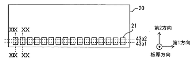
電極21は、基板20の一面20aに配置された複数の第1電極21aと、一面20aと反対の裏面20bに配置された複数の第2電極21bを有する。各電極21a,21bは、第1方向に沿って配列されている。また、板厚方向に直交する平面形状が矩形の基板20に対し、第2方向における一方の端部近傍である縁部22に形成されている。また、第2方向において、第1電極21aと第2電極21bは、ほぼ同じ位置に形成されている。第1電極21a及び第2電極21bは、第2方向において複数列配置させることもできるが、本実施形態では、ともに1列の配置となっている。
The
筺体30は、袋形状をなしており、第2方向における一端側に開口部31を有している。この筐体30には、基板20が収容されるとともに、コネクタ40の少なくとも一部も収容される。この筺体30は、PPSやPBTなどの合成樹脂材料や、アルミニウム等の金属材料を用いて形成される。筺体30は、1つの部材のみからなっても良いし、複数の部材を組み合わせて形成されるものでも良い。本実施形態では、樹脂を用いて形成された1つの部材によって筺体30が構成されており、第2方向に直交する断面の形状が略矩形となっている。すなわち、開口形状も略矩形となっている。また、図示しないが、筺体30の開口部31付近には、コネクタ40との嵌合部が設けられている。
The
コネクタ40は、PPSやPBTなどの合成樹脂材料を用いて形成されたハウジング41と、導電材料を用いて形成されるとともにハウジング41に保持された複数の端子42と、を有する。端子42の材料としては、導電性が良好な金属材料、例えばりん青銅をニッケルメッキで被覆し、さらに金メッキで被覆してなるものを採用することができる。
The
端子42は、第1電極21aに接触する複数の第1端子42aと、第2電極21bに接触する複数の第2端子42bと、を有している。各端子42(42a,42b)は導電材料を曲げ加工してなり、ハウジング41から基板20が収容された筐体30の内部空間32に突出する基板接続部43と、ハウジング41から内部空間32と反対の嵌合空間53に突出する外部接続部44と、を有している。さらに、端子42a,42bは、ハウジング41の図示しない孔に圧入固定された圧入部45を有している。外部接続部44は、外部コネクタ100がコネクタ40に嵌合された状態で、コンタクト103と電気的に接続される。
The terminal 42 includes a plurality of
基板接続部43は、図5に示すように、電極21(21a,21b)に接触する接点部43aと、該接点部43aよりも先端側の部分である先端部43bと、圧入部45と接点部43aとを繋ぐ繋ぎ部43cと、を有している。本実施形態では、端子42のうち、外部接続部44、圧入部45、及び基板接続部43における繋ぎ部43cの一部が、一体的に一直線状とされ、この一直線状の部分は、基板20の一面20aと略平行に配置される。また、基板接続部43の残りの部分、すなわち繋ぎ部43cの大部分、接点部43a、及び先端部43bは、略L字状をなしている。
As shown in FIG. 5, the
接点部43aは、第2方向において圧入部45と異なる位置とされるとともに、板厚方向において、圧入部45よりも基板20に近い位置とされている。また、先端部43bは、第2方向において接点部43aから離れるほど、板厚方向において基板20から離れるようなテーパ形状をなしている。また、繋ぎ部43cは、接点部43aから少なくとも一部と基板20の一面20a又は裏面20bとのなす角が鋭角となっている。本実施形態では、繋ぎ部43cのうち、略L字状をなす部分が、基板20の一面20a又は裏面20bとの間で鋭角をなす。換言すれば、L字状部分の繋ぎ部側端部が、鈍角をもって上記した一直線状部分の一端に連結されている。
The
また、後述する第1ハウジング部46と第2ハウジング部47の組み付け前後のいずれにおいても、先端部43bはハウジング41に接触しないように設けられている。このように、先端部43bは自由端となっており、基板接続部43は、ばね性を有している。このような端子42によれば、弾性変形した状態で、第1電極21aに第1端子42aの接点部43aが接触し、第2電極21bに第2端子42bの接点部43aが接触する。したがって、対応する電極21と端子42が電気的に接続されるとともに、基板20の両面側に位置する端子42a,42bの弾性変形による反力(付勢力)により、基板20が保持(固定)される。本実施形態では、第1端子42aと第2端子42bの構成がほぼ同一であるため、板厚方向において、第1端子42aにおけるハウジング41の保持部分と第2端子42bにおけるハウジング41の保持部分のほぼ中心位置に、基板20を保持することができる。このように、はんだ付けすることなく、端子42が電極21と電気的に接続される。
Further, the
ハウジング41は、板厚方向に分割された2つのハウジング部46,47からなる。板厚方向において、主として一面20a側に配置される第1ハウジング部46と、主として裏面20b側に配置される第2ハウジング部47は、互いに組み付けた状態で、それぞれの分割面46a,47aが全周でほぼ隙間なく合わさる。これにより、ハウジング41は、筺体30に収容された状態で、筐体30の内部空間32に異物が侵入しないように蓋をする。
The
第1ハウジング部46は、筒状部48と延設部49と、を有する。筒状部48は、その少なくとも一部が、袋形状をなす筐体30の内面30aと開口部31の周方向全周にわたって対向する。換言すれば、筐体30の開口部31周辺における内面30aの周形状に対応して筒状に設けられている。図4に示すように、本実施形態では、筒状部48が略矩形の筒形状をなし、筒状部48における第1方向の中央付近に、板厚方向に延びて筒を二分する仕切部48aが設けられている。すなわち、外部コネクタ100との接続口が2ポートとなっている。
The
延設部49は、筒状部48における内部空間32側の端部から延設されており、その全てが筺体30に収容される。すなわち、第2方向において、延設部49は筒状部48よりも筐体30の奥側に配置される。また、第2ハウジング部47は、その全てが筺体30に収容される。本実施形態では、ハウジング41が、筒状部48だけでなく、筒状部48よりも内部空間側にも筒を有し、この筒を板厚方向に直交する面で2分割した一方が延設部49、他方が第2ハウジング部47となっている。このため、延設部49は、図4に示すように、第2方向に直交する断面形状が略コの字状となっている。
The extending
また、第1ハウジング部46は、延設部49の内面から突出する第1壁部50を有している。第1壁部50は、その板厚方向が第2方向と略一致しており、この第1壁部50には、圧入により第1端子42aが保持されている。なお、本実施形態では、上記した仕切部48aによる2ポートに対応して、第1方向に並んで配置された2つの第1壁部50を有し、それぞれに第1端子42aが保持されている。また、延設部49が、第2方向において第1壁部50よりも内部空間32側に延設されており、この延設された部分を庇部49aと示す。
The
一方、第2ハウジング部47も、延設部49同様、図3に示すように、第2方向に直交する断面形状が略コの字状をなす基部51を有している。この基部51は、第1ハウジング部46と第2ハウジング部47を組み付けた状態で、延設部49とともに筒をなす。
On the other hand, as shown in FIG. 3, the
また、第2ハウジング部47は、コの字をなす基部51の底部内面から突出する第2壁部52を有している。第2壁部52は、その板厚方向が第2方向と略一致しており、この第2壁部52には、圧入により第2端子42bが保持されている。また、第2壁部52は、第2方向において第1壁部50と同じ位置に設けられている。第1壁部50の先端面と第2壁部52の先端面は、上記した分割面46a,47aの一部であり、第1ハウジング部46と第2ハウジング部47を組み付けた状態で、ほぼ隙間なく合わさる。そして、コネクタ40が筺体30に収容された状態で、壁部50,52よりも筺体30の奥側が内部空間32とされ、壁部50,52よりも開口部31側が、外部コネクタ100が嵌合される嵌合空間53となる。このように、壁部50,52は、内部空間32と嵌合空間53とを区画する。
The
なお、本実施形態では、上記した仕切部48aによる2ポートに対応して、第1方向に並んで配置された2つの第2壁部52を有し、それぞれに第2端子42bが保持されている。また、基部51が、第2方向において第2壁部52よりも内部空間32側に延設されており、この延設された部分を庇部51aと示す。
In addition, in this embodiment, it has the 2nd
このように構成されるハウジング41は、第1ハウジング部46と第2ハウジング部47との固定部としてスナップフィット54を有している。このスナップフィット54は、図3に示すように、板厚方向に延び、先端に係止爪を有する凸部55と、凸部55の係止爪が嵌る凹部56よりなる。凸部55は第2ハウジング部47の基部51及び庇部51aに設けられ、凹部56は第1ハウジング部46の延設部49及び庇部49aに設けられている。そして、凸部55の係止爪を、材料の弾性を利用して凹部56に嵌め込むことで、第1ハウジング部46と第2ハウジング部47が組み付けられ、ハウジング41が形成される。
The
このスナップフィット54は、図2〜図4に示すように、第1方向において、複数箇所に設けられている。具体的には、第1方向における両端と中央2箇所の計4箇所に設けられている。換言すれば、2つの第1壁部50(第2壁部52)に対して、それぞれの両端に設けられている。また、両端のスナップフィット54は、図5に示すように、第2方向において、電極21の形成範囲を跨ぐように設けられている。
As shown in FIGS. 2 to 4, the snap fits 54 are provided at a plurality of locations in the first direction. Specifically, it is provided in a total of four places, both ends in the first direction and two places in the center. In other words, the two first wall portions 50 (second wall portions 52) are provided at both ends. Further, as shown in FIG. 5, the snap fits 54 at both ends are provided so as to straddle the formation range of the
防水部材70は、例えばシリコンゴムからなり、ハウジング41のうち、筒状部48の外周面に沿って環状に設けられている。このため、筺体30にハウジング41が収容されると、防水部材70により、筺体30の内面30aとハウジング41の外周面との隙間から、筺体30の内部空間32に水分等が侵入するのを防ぐことができる。また、図示しないが、ハウジング41の外周面には、筺体30との嵌合部が設けられている。
The
次に、図6及び図7を用いて、上記した電子装置10の製造方法について説明する。
Next, a method for manufacturing the
先ず、図6に示すようにコネクタ40を組み付ける。このとき、基板20も保持される。板厚方向において、第1ハウジング部46、基板20、及び、第2ハウジング部47の順に配置し、互いに接触しない位置で、第1方向及び第2方向の位置合わせする。具体的には、第1端子42aの接点部43aが対応する第1電極21aにオーバーラップし、第2端子42bの接点部43aが、対応する第2電極21bにオーバーラップするようにする。そして、この位置合わせ状態で、第1ハウジング部46と第2ハウジング部47とを板厚方向において近づけ、スナップフィット54により固定する。これにより、ハウジング41、ひいてはコネクタ40が形成されるとともに、端子42a,42b間に基板20が保持される。
First, the
次に、図7に示すように基板20及びコネクタ40を筺体30に収容する。すなわち、電子装置10を組み付ける。基板20を先頭として、基板20及びコネクタ40を筺体30内に挿入する。そして、図示しない嵌合部同士が嵌合することで、コネクタ40が筺体30に固定される。この状態で、筒状部48に配置された防水部材70により、筐体30の内面30aとハウジング41の外面は水密となる。以上により、図1に示す電子装置10が形成される。
Next, as shown in FIG. 7, the
次に、本実施形態に係る電子装置10の特徴部分について、その作用効果を説明する。
Next, the effect of the characteristic part of the
本実施形態では、ハウジング41を第1ハウジング部46と第2ハウジング部47に分割し、これらハウジング部46,47を板厚方向に組み付けることでハウジング41をなす構造とした。また、第1ハウジング部46に第1端子42aを設け、第2ハウジング部47に第2端子42bを設けたので、板厚方向に組み付けてハウジング41を形成する際に、板厚方向から、第1端子42aを第1電極21aに接触させ、第2端子42bを第2電極21bに接触させることができる。このため、端子42を電極21に接触させる際に、例えば基板20のエッジに端子42の接点部43aが接触しない。したがって、端子42の損傷や変形などを抑制し、ひいては接続信頼性の低下を抑制することができる。
In the present embodiment, the
また、第1ハウジング部46は、袋形状をなす筐体30の内面30aと開口部31の周方向全周にわたって対向する筒状部48を有しており、この筒状部48と筐体30の間に防水部材70が配置される。したがって、ハウジング41と筺体30との間の水密を確保することができる。なお、第1ハウジング部46が筒状部48を有さず、第1ハウジング部46と第2ハウジング部47が板厚方向において完全に2分割された構造とすると、防水部材70は、第1ハウジング部46と第2ハウジング部47の分割面46a,47aを跨いで配置されることとなる。このため、筐体30とコネクタ40のハウジング41との防水以外に、コネクタ40の分割面46a,47aの防水も必要となる。したがって、本実施形態のほうが容易に防水性を確保することができる。
Further, the
また、第1ハウジング部46と第2ハウジング部47との分割面46a,47aは、全周でほぼ隙間なく合わさり、ハウジング41は、内部空間32を蓋するように配置される。このため、ハウジング41の分割構造を採用しながらも、外部コネクタ100が接続される前の状態において、電子装置10の内部空間32に異物が侵入するのを抑制することができる。しかしながら、分割面46a,47aを全周でほぼ隙間なく合わせることは必須ではない。外部コネクタ100がコネクタ40に嵌合すると、外部コネクタ100の防水部材105により、筒状部48とハウジング101の間に水密が形成される。したがって、分割面46a,47aに隙間があっても、外部コネクタ100が嵌合した状態では、内部空間32を防水空間とすることができる。
Further, the dividing surfaces 46 a and 47 a of the
また、基板接続部43が、接点部43aと先端部43bと繋ぎ部43cを有し、接点部43aは、第2方向において、圧入部45と異なる位置とされるとともに、板厚方向において、圧入部45よりも基板20に近い位置とされている。また、繋ぎ部43cの接点部43aから少なくとも一部と基板20の一面20a又は裏面20bとのなす角は鋭角とされている。そして、先端部43bは、少なくとも第1ハウジング部46と第2ハウジング部47を組み付ける前の状態で、保持されているハウジング部46,47に対して離間している。このように、組み付け前の状態で先端部43bがフリーであるため、図8に示すように、組み付けにより基板接続部43が板厚方向に撓むと、接点部43aは基板20(第2電極21b)の表面に接触しつつ第2方向へスライドする。したがって、接点部43a及び第2電極21b表面をワイピングし、表面の酸化物層を除去することができる。なお、図8の破線が、接点部43aが対応する第2電極21bに接触した組み付け初期を示し、実線が、組み付けにより基板接続部43が板厚方向に撓んだ状態を示している。図8では、第2端子42bと第2電極21bのみを示しているが、第1端子42aと第1電極21aについても同様である。
The
さらに本実施形態では、基板接続部43が折り返し形状を有しており、接点部43aが弧状となっている。したがって、図9に示すように、基板接続部43は、組み付けにより板厚方向に撓むとともに少なからず回転運動し、弧状部分において接点部43aが変位する。図9で示す破線は、回転運動する前の接点部43aの位置を示している。この回転運動によっても、ワイピングすることができる。
Further, in the present embodiment, the
また、第1ハウジング部46と第2ハウジング部47とは、スナップフィット54により組み付けられる。ねじ締結や接着固定に較べて、別部品不要であり、構成を簡素化することができる。また、製造工程も簡素化できる。しかしながら、スナップフィット54以外の組み付け方法も採用することができる。例えば上記のようにねじ締結により、板厚方向において第1ハウジング部46を第2ハウジング部47に組み付けても良い。また、接着剤により、板厚方向において第1ハウジング部46を第2ハウジング部47に組み付けても良い。
Further, the
(第1変形例)
上記実施形態では、第1ハウジング部46及び第2ハウジング部47が、それぞれ庇部49a,51aを有する例を示した。しかしながら、図10に示すように、第1ハウジング部46及び第2ハウジング部47が、それぞれ庇部49a,51aを有さない構成としても良い。さらには、第1ハウジング部46及び第2ハウジング部47の一方が庇部を有し、他方が庇部を有さない構成としても良い。
(First modification)
In the said embodiment, the
(第2実施形態)
本実施形態において、上記実施形態に示した電子装置10と共通する部分についての説明は割愛する。
(Second Embodiment)
In the present embodiment, the description of the parts common to the
本実施形態の特徴は、コネクタ40が、少なくとも第1ハウジング部46と第2ハウジング部47を組み付ける前の状態で、第1ハウジング部46及び第2ハウジング部47の一方における所定位置に基板20を保持する保持部57を有することにある。それ以外の点は、第1実施形態と同じである。
The feature of this embodiment is that the
本実施形態では、図11〜図13に示すように、保持部57が、第1ハウジング部46に設けられた係止部57aと、第1ハウジング部46に保持された第1端子42aにより構成されている。
In the present embodiment, as shown in FIGS. 11 to 13, the holding
係止部57aは、第1ハウジング部46の一部として構成されており、第1方向において、電極21の形成範囲よりも外側において基板20を保持するように設けられている。また、係止部57aは、庇部49aを含む延設部49から、板厚方向において第1壁部50と同方向に突出しており、弾性変形可能に設けられている。係止部57aにおける基板20の裏面20bに接触する部分は、板厚方向において第1端子42aの接点部43aよりも延設部49から離れた位置となっている。そして、第1端子42aにおける基板接続部43のばね力により、係止部57aと第1端子42aの間で基板20を挟持することで、第1ハウジング部46に基板20が保持される。基板20の保持位置は、第1端子42aと第2端子42bのばね力の釣り合い位置よりも、板厚方向において延設部49から離れた位置となっている。
The locking
なお、基板20の保持は、第1ハウジング部46と第2ハウジング部47の組み付けの前に実行される。基板20を係止部57aと第1端子42aで挟む際には、基板20が第1端子42aに接触しないように基板20を斜めにしながら係止部57aに係止させる。このとき係止部57aを弾性変形させながら基板20を係止させ、その状態で係止部分を支点として基板20を回転させ、第1電極21aを第1端子42aの接点部43aに接触させる。これにより、基板20のエッジに第1端子42aの接点部43aを接触させることなく、基板20を保持することができる。
The holding of the
また、基板20が第1ハウジング部46に保持された状態で、第1ハウジング部46と第2ハウジング部47を組み付ける。この組み付け状態では、図14に示すように、第1端子42aと第2端子42bにより基板20が保持される。第1実施形態同様、第1端子42aと第2端子42bの構成はほぼ同じであり、基板20は板厚方向において第1端子42aと第2端子42bのばね力が釣り合う位置まで変位する。これにより、基板20は延設部49に近づき、係止部57aが基板20に対して離間される。このように、第1ハウジング部46と第2ハウジング部47を組み付けた状態では、端子42a,42bにより基板20が保持され、保持部57による保持は解除される。
Further, the
このように本実施形態では、保持部57により基板20を保持した状態で、第1ハウジング部46と第2ハウジング部47を組み付けるため、保持しない場合に較べて、ハウジング41を形成しつつ端子42と電極21との電気的な接続構造を形成しやすい。また、ハウジング41に対する基板20の位置精度を向上することができる。このため、端子42が対応する電極21に対してより確実に接触することとなり、これによっても接続信頼性の低下を抑制することができる。
As described above, in the present embodiment, the
特に本実施形態では、端子42のばね力を利用して基板20を保持するため、ねじ締結や接着に較べて、保持部57の構成を簡素化することができる。また、製造工程を簡素化することができる。
In particular, in this embodiment, since the board |
また、第1ハウジング部46と第2ハウジング部47を組み付けた状態で、係止部57aは基板20に非接触となるため、第1端子42aと第2端子42bで接圧(接触荷重)が異なるのを抑制することができる。これにより、接続信頼性の低下を抑制することができる。
Further, in the state where the
なお、保持部57は、第1ハウジング部46及び第2ハウジング部47のいずれか一方に設けられれば良い。したがって、第2ハウジング部47に設けられても良い。また、保持部57の構成も、係止部57aと端子42による挟持に限定されるものではない。ねじ締結や接着により、例えば第1ハウジング部46に保持しても良い。この場合、保持部57によって基板20の位置が決定することとなる。
Note that the holding
(第2変形例)
上記実施形態では、第1ハウジング部46が、その一部として係止部57aを有する例を示した。しかしながら、第1ハウジング部46に金属部材を保持させ、この金属部材を係止部としても良い。例えば図15に示す例では、電気的な接続機能を提供しないダミー端子を、係止部57bとしている。図15において、第1壁部50は、板厚方向において、第1端子42aと第2端子42bの釣り合う位置よりも上方に突出している。係止部57bは端子42と同一材料を用いて形成されており、基板20の裏面20bに係止する。そして、第1端子42aのばね力により、係止部57bと第1端子42aの間で基板20が挟持される。この場合も、基板20の保持位置は、第1端子42aと第2端子42bのばね力の釣り合い位置よりも、板厚方向において延設部49から離れた位置となっている。そして、上記実施形態同様、第1ハウジング部46と第2ハウジング部47を組み付けた状態で、端子42a,42bにより基板20が保持され、保持部57による保持は解除される。
(Second modification)
In the said embodiment, the
(第3実施形態)
本実施形態において、上記実施形態に示した電子装置10と共通する部分についての説明は割愛する。
(Third embodiment)
In the present embodiment, the description of the parts common to the
本実施形態の特徴は、図16及び図17に示すように、筐体30が、開口部31から所定範囲の部分であり、第2方向に直交する開口面積の大きい拡径部33と、該拡径部33よりも開口面積の小さい縮径部34と、拡径部33と縮径部34を繋ぐテーパ部35と、を有している。テーパ部35は、第2方向においてその開口面積が連続的に変化しており、拡径部33側から縮径部34側に向けて開口面積が減少している。そして、第1ハウジング部46と第2ハウジング部47は、それぞれテーパ部35に接触することで、組み付けられるようになっていることにある。なお、それ以外の点は、第1実施形態とほぼ同じである。
As shown in FIGS. 16 and 17, the feature of the present embodiment is that the
本実施形態では、図22及び図23に示すように、第1ハウジング部46の延設部49のうち、筒状部48と反対の端部における外面側の角部もテーパ部58となっている。また、第2ハウジング部47の基部51のうち、筒状部48と反対の端部における外面側の角部もテーパ部58となっている。ハウジング41において、これらテーパ部58を有する部分の外形は、筒状部48に近いほど大きく、筒状部48から離れるほど小さくなっている。また、テーパ部58は、筐体30のテーパ部35とほぼ同じ傾きを有している。
In the present embodiment, as shown in FIGS. 22 and 23, the corner portion on the outer surface side at the end opposite to the
なお、図16に示す符号59は、凸部である。第1ハウジング部46と第2ハウジング部47を組み付けた状態で、ハウジング41は、板厚方向におけるほぼ中心部分に、嵌合空間53側に突出する凸部59を有する。この凸部59は、第1ハウジング部46の第1壁部50の一部と、第2ハウジング部47の第2壁部52の一部により構成される。凸部59の裏側は第1ハウジング部46の前面50a及び第2ハウジング部47の前面52aに開口する凹みになっており、この凹みに基板20の端部が挿入配置される。また、端子42(42a,42b)は、第1壁部50及び第2壁部52の前面50a,52aに形成された図示しない溝に圧入されている。すなわち、圧入部45が、前面50a,52aに位置する。そして、基板接続部43は前面50a,52a側から上記した凸部59裏側の凹みに配置されている。
In addition, the code |
このように構成される電子装置10では、第1端子42aが基板20の第1電極21aに接触し、第2端子42bが第2電極21bに接触するように、第1ハウジング部46、第2ハウジング部47、及び基板20を位置決めする。このとき、図示しない治具を、凸部59を構成する第1ハウジング部46側の側面59aと第2ハウジング部47側の側面59bに接触させて板厚方向に挟み、ハウジング41を保持する。そして、この位置決め状態で、第2方向において筐体30の内部に基板20側からコネクタ40を挿入する。すると、コネクタ40のテーパ部58の外面が筐体30のテーパ部35の内面に接触する。さらに筐体30の奥側にコネクタ40を押し込むと、図17に実線矢印で例示するように、各ハウジング部46,47に対して筐体30から押さえつける力が作用する。これにより、第1ハウジング部46と第2ハウジング部47とは、板厚方向において筐体30により挟持される形となり、第1ハウジング部46に第2ハウジング部47が組み付けられる。また、第1ハウジング部46と第2ハウジング部47の組み付けにより、端子42が対応する電極21にしっかり接触し、端子42と電極21が電気的に接続される。また、第1端子42aと第2端子42bのばね力により、基板20が保持される。
In the
このように、筐体30を利用した第1ハウジング部46と第2ハウジング部47の組み付け構造を採用しても、別部品を不要とすることができるので、構成を簡素化することができる。
Thus, even if the assembly structure of the
なお、上記実施形態では、筐体30にテーパ部35を設けるとともに、ハウジング41にもテーパ部58を設ける例を示したが、ハウジング41がテーパ部58を有さず、筐体30のみがテーパ部35を有する構成としても良い。
In the above embodiment, the
(第4実施形態)
本実施形態において、上記実施形態に示した電子装置10と共通する部分についての説明は割愛する。
(Fourth embodiment)
In the present embodiment, the description of the parts common to the
本実施形態の特徴は、第1端子42aの接点部43aは、第2方向において複数列とされ、第2端子42bの接点部43aは、第2方向において第1端子と同数の複数列とされることにある。それ以外の点は、第1実施形態と同じである。
The feature of this embodiment is that the
図18〜図20に示す例では、第1端子42a及び第2端子42bともに、第2方向において基板20の端部に近い第1接点部43a1と、第2接点部43a2の2列配置となっている。具体的には、電極21を第2方向において長い形状とし、第1接点部43a1と第2接点部43a2で接触位置をずらした。また、第1方向において、第1接点部43a1と第2接点部43a2を交互に設けた。
In the example shown in FIGS. 18 to 20, both the first terminal 42 a and the
第2方向において接点部43aを1列とすると、第1ハウジング部46と第2ハウジング部47の組み付け時に第2方向の位置ずれが生じると、第1端子42aと第2端子42bの接点部43aも第2方向で位置がずれるため、回転モーメントが発生する。これに対し、本実施形態に示すように接点部43aを第2方向において複数列とする、すなわち接点部43aにより押さえられる基板20の幅を広くすると、回転モーメントを低減することができる。なお、接点部43aの配置は2列に限定されるものではなく、3列以上としても良い。
When the
(第3変形例)
上記実施形態では、電極21は第2方向において1列配置である例を示した。しかしながら、例えば図21に示すように、電極21を複数例(例えば2列)とし、これにより、接点部43aを、第1接点部43a1と第2接点部43a2の2列配置としても良い。
(Third Modification)
In the above embodiment, an example in which the
(第5実施形態)
本実施形態において、上記実施形態に示した電子装置10と共通する部分についての説明は割愛する。
(Fifth embodiment)
In the present embodiment, the description of the parts common to the
本実施形態の特徴は、第1ハウジング部46及び第2ハウジング部47は、板厚方向における筐体30との対向部分にばね部60をそれぞれ有している。そして、ばね部60は、板厚方向に弾性変形しつつ筐体30の内面30aにそれぞれ接触することにある。それ以外の点は、第1実施形態と同じである。
The feature of this embodiment is that the
図22及び図23では、第2ハウジング部47を例示している。ばね部60は、第2ハウジング部47の一部として、基部51における第2壁部52の突出面と反対の面、すなわち上面51bに設けられている。また、ばね部60は板厚方向に弾性変形可能に設けられており、複数のばね部60が、第1方向に沿って配列されている。複数のばね部60の形成範囲は、端子42の配列範囲とほぼ一致している。なお、図示しないが、第1ハウジング部46の延設部49にも同様にばね部60が形成されている。
22 and 23 illustrate the
このような構成を採用すると、ハウジング41のばね部60によって、端子42のばね力を補うことができる。すなわち、端子42のばね力を小さくすることができるので、基板接続部43の長さ(ばね長)を短くし、体格を小型化することができる。図24(a)はばね部60を有さない従来の端子42を示し、図24(b)は本実施形態の端子42を示している。したがって、圧入部45よりも接点部43a側が基板接続部43である。このように、本実施形態によれば、端子42の基板接続部43を短くすることができる。
When such a configuration is employed, the spring force of the terminal 42 can be supplemented by the
例えば、図24(b)に示すように、基板接続部43の先端に接触部43dを設け、図25に示すように、第1ハウジング部46と第2ハウジング部47を組み付ける前の状態で、接触部43dが第2ハウジング部47の受け面61に接触する構成としても良い。この場合、端子42は、圧入部45と接触部43dによって板厚方向への変位が制限され、組み付け時には、基板接続部43のうち、接点部43aを含む一部分がわずかに撓む程度である。このため、ばね部60が接圧の殆どを担うこととなる。なお、図25では、第2ハウジング部47側を例示するが、第1ハウジング部46においても同様である。
For example, as shown in FIG. 24 (b), a
また、ばね部60を有さない構成では、経時的な応力緩和により、端子42の接圧が低下するのを抑制するために、端子42の材料として高価なもの、具体的には応力緩和しにくい耐熱用銅合金を採用している。これに対し、本実施形態では、ばね部60によって経時的な応力緩和による接圧の低下を抑制することができるため、端子42を従来よりも安い材料を用いて形成することができる。
Further, in the configuration without the
(第4変形例)
ハウジング41がばね部60を有する構成において、第2端子42bの接触部43dが、組み付け前の状態で、すでに第2ハウジング部47の受け面61に接触する例を示した。この場合、上記したように、基板接続部43は、接点部43aを含む一部分が、板厚方向においてわずかに撓む程度であり、図8及び図9に示したようなワイピングの効果を望めない。したがって、ばね部60を有する構成においても、図26に示すように、第1ハウジング部46と第2ハウジング部47の組み付け前の状態で、第2端子42bの接点部43a及び先端部43bが、第2ハウジング部47に接触しない構成とすると良い。このようにすると、図8及び図9に示したように、第1ハウジング部46と第2ハウジング部47の組み付け時に、ワイピングすることができる。なお、図27では、第1ハウジング部46と第2ハウジング部47の組み付けた状態で、第2端子42bの接触部43dが第2ハウジング部47の受け面61に接触している。図27に示す破線は、図26に示す接点部43aの位置を示している。このような構成では、図28に示すように、コネクタ組み付け時、すなわち第1ハウジング部46と第2ハウジング部47の組み付け時に、板厚方向において端子42が弾性変形し、端子42によっても所定の接圧(接触加重)を確保することができる。また、筐体30を組み付ける際に、第1方向に並設された複数のばね部60が、板厚方向に弾性変形するため、ばね部60によって接圧を大きく稼ぐことができる。換言すれば、端子42のばね力はワイピングできる分とし、ワイピング完了後は、ばね部60で接圧を確保することができる。
(Fourth modification)
In the configuration in which the
なお、図27では、第1ハウジング部46と第2ハウジング部47の組み付け時に、第2端子42bの接触部43dが第2ハウジング部47の受け面61に接触する例を示したが、第1実施形態などで示したように、組み付け後も接点部43a及び先端部43bが第2ハウジング部47に接触しない構成としても良い。また、上記例では、第2ハウジング部47側を示したが、第1ハウジング部46においても同様である。
27 shows an example in which the
以上、本発明の好ましい実施形態について説明したが、本発明は上述した実施形態になんら制限されることなく、本発明の主旨を逸脱しない範囲において、種々変形して実施することが可能である。 The preferred embodiments of the present invention have been described above. However, the present invention is not limited to the above-described embodiments, and various modifications can be made without departing from the spirit of the present invention.
10・・・電子装置、20・・・基板、20a・・・一面、20b・・・裏面、21・・・電極、21a・・・第1電極、21b・・・第2電極、22・・・縁部、30・・・筺体、30a・・・内面、31・・・開口部、32・・・内部空間、33・・・拡径部、34・・・縮径部、35・・・テーパ部、40・・・コネクタ、41・・・ハウジング、42・・・端子、42a・・・第1端子、42b・・・第2端子、43・・・基板接続部、43a・・・接点部、43a1・・・第1接点部、43a2・・・第2接点部、43b・・・先端部、43c・・・繋ぎ部、43d・・・接触部、44・・・外部接続部、45・・・圧入部、46・・・第1ハウジング部、47・・・第2ハウジング部、46a,47a・・・分割面、48・・・筒状部、48a・・・仕切部、49・・・延設部、49a・・・庇部、50・・・第1壁部、50a・・・前面、51・・・基部、51a・・・庇部、51b・・・上面、52・・・第2壁部、52a・・・前面、53・・・嵌合空間、54・・・スナップフィット、55・・・凸部、56・・・凹部、57・・・保持部、57a,57b・・・係止部、58・・・テーパ部、59・・・凸部、59a,59b・・・側面、60・・・ばね部、61・・・受け面、70・・・防水部材、100・・・外部コネクタ、101・・・ハウジング、101a・・・前面、101b・・・側面、101c・・・後面、102・・・孔、103・・・コンタクト、104・・・ワイヤーハーネス、105,107・・・防水部材、106・・・溝部、108・・・蓋部、
DESCRIPTION OF
Claims (13)
開口部(31)を有し、前記基板(20)を収容する袋形状の筐体(30)と、
合成樹脂材料を用いて形成されたハウジング(41)と、導電材料を用いて形成されるとともに前記ハウジング(41)に保持され、前記ハウジング(41)から前記基板(20)が収容された前記筐体(30)の内部空間(32)に突出する基板接続部(43)、及び、前記ハウジング(41)から前記内部空間(32)と反対の嵌合空間(53)に突出する外部接続部(44)を備える複数の端子(42)と、有するコネクタ(40)と、
前記筐体(30)と前記ハウジング(41)との間に配置され、前記筐体(30)と前記ハウジング(41)との間から前記内部空間(32)に水分が侵入するのを抑制する防水部材(70)と、を備え、
前記電極(21)は、前記基板の一面(20a)に配置された複数の第1電極(21a)と、前記一面(20a)と反対の裏面(20b)に配置された複数の第2電極(21b)と、を有し、
複数の前記端子(42)は、前記第1電極(21a)に接触する複数の第1端子(42a)と、前記第2電極(21b)に接触する複数の第2端子(42b)と、を有し、
前記基板(20)の両面(20a,20b)において前記電極(21)に前記端子(42)が接触することで、前記電極(21)と前記端子(42)とが電気的に接続されるとともに、前記第1端子(42a)と前記第2端子(42b)の間に前記基板(20)が保持され、
前記ハウジング(41)は、少なくとも一部が前記筐体(30)の内面(30a)全周に沿って配置される筒状部(48)と、該筒状部(48)における前記内部空間(32)側の端部から延設され、前記筐体(30)に収容される延設部(49)と、前記延設部(49)の内面から突出する第1壁部(50)と、を有する第1ハウジング部(46)と、前記第1ハウジング部(46)に対して前記基板(20)の板厚方向に組み付けられ、前記第1ハウジング部(46)とともに前記ハウジング(41)をなすものであって、組み付けた状態で前記延設部(49)とともに前記筒状部(48)に連なる筒をなし、前記筐体(30)に収容される基部(51)と、前記基部(51)の内面から突出する第2壁部(52)と、を有する第2ハウジング部(47)と、を有し、
前記第1壁部(50)及び前記第2壁部(52)により、前記内部空間(32)と前記嵌合空間(53)とが区画され、
前記第1壁部(50)に前記第1端子(42a)が保持されるとともに、前記第2壁部(52)に前記第2端子(42b)が保持されて、複数の前記端子(42)の外部接続部(44)が、前記ハウジング(41)における前記嵌合空間(53)側の共通の筒内に配置され、
前記防水部材(70)は、前記筒状部(48)と前記筐体(30)との間に介在されることを特徴とする電子装置。 A substrate (20) having electrodes (21) on both sides (20a, 20b);
A bag-shaped housing (30) having an opening (31) and accommodating the substrate (20);
A housing (41) formed using a synthetic resin material, and the housing formed using a conductive material and held in the housing (41), in which the substrate (20) is accommodated from the housing (41). A board connecting part (43) protruding into the internal space (32) of the body (30) and an external connecting part (53) protruding from the housing (41) into the fitting space (53) opposite to the internal space (32) 44) a plurality of terminals (42) having a connector (40);
It arrange | positions between the said housing | casing (30) and the said housing (41), and suppresses that a water | moisture content penetrate | invades into the said internal space (32) from between the said housing | casing (30) and the said housing (41). A waterproof member (70),
The electrode (21) includes a plurality of first electrodes (21a) disposed on one surface (20a) of the substrate and a plurality of second electrodes (20b) disposed on the back surface (20b) opposite to the one surface (20a). 21b)
The plurality of terminals (42) include a plurality of first terminals (42a) in contact with the first electrode (21a) and a plurality of second terminals (42b) in contact with the second electrode (21b). Have
When the terminal (42) is in contact with the electrode (21) on both surfaces (20a, 20b) of the substrate (20), the electrode (21) and the terminal (42) are electrically connected. The substrate (20) is held between the first terminal (42a) and the second terminal (42b),
The housing (41) includes at least a part of the cylindrical part (48) disposed along the entire circumference of the inner surface (30a) of the housing (30), and the internal space in the cylindrical part (48) ( 32) an extended portion (49) extending from the end on the side and housed in the housing (30), a first wall portion (50) protruding from the inner surface of the extended portion (49), A first housing part (46) having the following structure: assembled to the first housing part (46) in the thickness direction of the substrate (20), and the housing (41) together with the first housing part (46). be one to name, a tubular continuous with the tubular portion (48) wherein with extended portion (49) in a state where the assembled, a base (51) which is accommodated in the housing (30), said base second wall portion projecting from the inner surface (51) and (52), second Howe having A ring portion (47), a
The internal space (32) and the fitting space (53) are partitioned by the first wall portion (50) and the second wall portion (52),
The first terminal (42a) is held on the first wall (50) , and the second terminal (42b) is held on the second wall (52 ). Are disposed in a common cylinder on the side of the fitting space (53) in the housing (41),
The electronic device according to claim 1, wherein the waterproof member (70) is interposed between the tubular portion (48) and the housing (30).
開口部(31)を有し、前記基板(20)を収容する袋形状の筐体(30)と、
合成樹脂材料を用いて形成されたハウジング(41)と、導電材料を用いて形成されるとともに前記ハウジング(41)に保持され、前記ハウジング(41)から前記基板(20)が収容された前記筐体(30)の内部空間(32)に突出する基板接続部(43)、及び、前記ハウジング(41)から前記内部空間(32)と反対の外部(53)に突出する外部接続部(44)を備える複数の端子(42)と、有するコネクタ(40)と、
前記筐体(30)と前記ハウジング(41)との間に配置され、前記筐体(30)と前記ハウジング(41)との間から前記内部空間(32)に水分が侵入するのを抑制する防水部材(70)と、を備え、
前記電極(21)は、前記基板の一面(20a)に配置された複数の第1電極(21a)と、前記一面(20a)と反対の裏面(20b)に配置された複数の第2電極(21b)と、を有し、
前記端子(42)は、前記第1電極(21a)に接触する複数の第1端子(42a)と、前記第2電極(21b)に接触する複数の第2端子(42b)と、を有し、
前記基板(20)の両面(20a,20b)において前記電極(21)に前記端子(42)が接触することで、前記電極(21)と前記端子(42)とが電気的に接続されるとともに、前記第1端子(42a)と前記第2端子(42b)の間に前記基板(20)が保持され、
前記ハウジング(41)は、少なくとも一部が前記筐体(30)の内面(30a)全周に沿って配置される筒状部(48)と、該筒状部(48)における前記内部空間(32)側の端部から延設され、前記筐体(30)に収容される延設部(49)と、を有する第1ハウジング部(46)と、前記第1ハウジング部(46)に対して前記基板(20)の板厚方向に組み付けられ、前記第1ハウジング部(46)とともに前記ハウジング(41)をなす第2ハウジング部(47)と、を有し、
前記第1ハウジング部(46)に前記第1端子(42a)が保持されるとともに、前記第2ハウジング部(47)に前記第2端子(42b)が保持されており、
前記防水部材(70)は、前記筒状部(48)と前記筐体(30)との間に介在され、
前記コネクタ(40)は、少なくとも前記第1ハウジング部(46)と前記第2ハウジング部(47)を組み付ける前の状態で、前記第1ハウジング部(46)及び前記第2ハウジング部(47)の一方における所定位置に前記基板(20)を保持する保持部(57)を有することを特徴とする電子装置。 A substrate (20) having electrodes (21) on both sides (20a, 20b);
A bag-shaped housing (30) having an opening (31) and accommodating the substrate (20);
A housing (41) formed using a synthetic resin material, and the housing formed using a conductive material and held in the housing (41), in which the substrate (20) is accommodated from the housing (41). A board connection part (43) protruding into the internal space (32) of the body (30) and an external connection part (44) protruding from the housing (41) to the outside (53) opposite to the internal space (32). A plurality of terminals (42) comprising: a connector (40) comprising:
It arrange | positions between the said housing | casing (30) and the said housing (41), and suppresses that a water | moisture content penetrate | invades into the said internal space (32) from between the said housing | casing (30) and the said housing (41). A waterproof member (70),
The electrode (21) includes a plurality of first electrodes (21a) disposed on one surface (20a) of the substrate and a plurality of second electrodes (20b) disposed on the back surface (20b) opposite to the one surface (20a). 21b)
The terminal (42) has a plurality of first terminals (42a) in contact with the first electrode (21a) and a plurality of second terminals (42b) in contact with the second electrode (21b). ,
When the terminal (42) is in contact with the electrode (21) on both surfaces (20a, 20b) of the substrate (20), the electrode (21) and the terminal (42) are electrically connected. The substrate (20) is held between the first terminal (42a) and the second terminal (42b),
The housing (41) includes at least a part of the cylindrical part (48) disposed along the entire circumference of the inner surface (30a) of the housing (30), and the internal space ( 32) a first housing part (46) having an extension part (49) that extends from the end on the side and is accommodated in the housing (30), and the first housing part (46) A second housing part (47) assembled in the thickness direction of the substrate (20) and forming the housing (41) together with the first housing part (46),
The first terminal (42a) is held by the first housing part (46), and the second terminal (42b) is held by the second housing part (47),
The waterproof member (70) is interposed between the tubular portion (48) and the housing (30) ,
The connector (40) has at least the first housing part (46) and the second housing part (47) in a state before assembling the first housing part (46) and the second housing part (47). electronic device according to claim Rukoto that having a holding portion (57) for holding the substrate (20) in position on one.
前記第1ハウジング部(46)と前記第2ハウジング部(47)を組み付けた状態で、前記係止部(57a)は、前記基板(20)に対して離間されることを特徴とする請求項2又は請求項3に記載の電子装置。 The holding portion (57) includes a locking portion (57a) provided on one of the first housing portion (46) and the second housing portion (47), and the housing having the locking portion (57a). The substrate (20) is held between the locking portion (57a) and the terminal (42) by the spring force of the terminal (42). ,
Wherein in a first state in which the assembled housing unit and the second housing portion (46) to (47), the locking portion (57a) is claim, characterized in that it is spaced the relative substrate (20) The electronic device according to claim 2 or claim 3 .
前記ハウジング(41)は、前記内部空間(32)を蓋することを特徴とする請求項1〜4いずれか1項に記載の電子装置。 The dividing surfaces (46a, 47a) of the first housing part (46) and the second housing part (47) are joined together without any gaps on the entire circumference,
The electronic device according to claim 1 , wherein the housing (41) covers the internal space (32).
複数の前記端子(42)は、前記板厚方向に直交する第1方向に沿って配置されており、
前記接点部(43a)は、前記板厚方向及び前記第1方向の両方向に直交する第2方向において、前記圧入部(45)と異なる位置とされるとともに、前記板厚方向において、前記圧入部(45)よりも前記基板(20)に近い位置とされ、
前記繋ぎ部(43c)の前記接点部(43a)から少なくとも一部と前記基板(20)の一面(20a)又は裏面(20b)とのなす角は鋭角とされ、
前記先端部(43b)は、少なくとも前記第1ハウジング部(46)と前記第2ハウジング部(47)を組み付ける前の状態で、保持されている前記ハウジング部に対して離間することを特徴とする請求項1〜5いずれか1項に記載の電子装置。 The board connection part (43) includes a contact part (43a) that contacts the electrode (21), a tip part (43b) that is a part on the tip side of the contact part (43a), and the terminal (42). A press-fitting part (45) held in the housing (41) and a connecting part (43c) connecting the contact part (43a),
The plurality of terminals (42) are arranged along a first direction orthogonal to the plate thickness direction,
The contact portion (43a) is located at a position different from the press-fit portion (45) in a second direction perpendicular to both the plate thickness direction and the first direction, and the press-fit portion in the plate thickness direction. It is a position closer to the substrate (20) than (45),
An angle formed by at least a part of the connecting portion (43c) from the contact portion (43a) and one surface (20a) or the back surface (20b) of the substrate (20) is an acute angle,
The tip portion (43b) is separated from the held housing portion at least before the first housing portion (46) and the second housing portion (47) are assembled. The electronic device according to claim 1 .
前記第1ハウジング部(46)と前記第2ハウジング部(47)は、それぞれ前記テーパ部(35)に接触して組み付けられることを特徴とする請求項1〜6いずれか1項に記載の電子装置。 The housing (30) is a portion within a predetermined range from the opening (31), and has a large diameter portion (33) having a large opening area and a reduced diameter portion having a smaller opening area than the large diameter portion (33). (34) and a tapered portion (35) connecting the enlarged diameter portion (33) and the reduced diameter portion (34),
The electron according to any one of claims 1 to 6, wherein the first housing part (46) and the second housing part (47) are assembled in contact with the tapered part (35), respectively. apparatus.
開口部(31)を有し、前記基板(20)を収容する袋形状の筐体(30)と、
合成樹脂材料を用いて形成されたハウジング(41)と、導電材料を用いて形成されるとともに前記ハウジング(41)に保持され、前記ハウジング(41)から前記基板(20)が収容された前記筐体(30)の内部空間(32)に突出する基板接続部(43)、及び、前記ハウジング(41)から前記内部空間(32)と反対の外部(53)に突出する外部接続部(44)を備える複数の端子(42)と、有するコネクタ(40)と、
前記筐体(30)と前記ハウジング(41)との間に配置され、前記筐体(30)と前記ハウジング(41)との間から前記内部空間(32)に水分が侵入するのを抑制する防水部材(70)と、を備え、
前記電極(21)は、前記基板の一面(20a)に配置された複数の第1電極(21a)と、前記一面(20a)と反対の裏面(20b)に配置された複数の第2電極(21b)と、を有し、
前記端子(42)は、前記第1電極(21a)に接触する複数の第1端子(42a)と、前記第2電極(21b)に接触する複数の第2端子(42b)と、を有し、
前記基板(20)の両面(20a,20b)において前記電極(21)に前記端子(42)が接触することで、前記電極(21)と前記端子(42)とが電気的に接続されるとともに、前記第1端子(42a)と前記第2端子(42b)の間に前記基板(20)が保持され、
前記ハウジング(41)は、少なくとも一部が前記筐体(30)の内面(30a)全周に沿って配置される筒状部(48)と、該筒状部(48)における前記内部空間(32)側の端部から延設され、前記筐体(30)に収容される延設部(49)と、を有する第1ハウジング部(46)と、前記第1ハウジング部(46)に対して前記基板(20)の板厚方向に組み付けられ、前記第1ハウジング部(46)とともに前記ハウジング(41)をなす第2ハウジング部(47)と、を有し、
前記第1ハウジング部(46)に前記第1端子(42a)が保持されるとともに、前記第2ハウジング部(47)に前記第2端子(42b)が保持されており、
前記防水部材(70)は、前記筒状部(48)と前記筐体(30)との間に介在され、
前記筐体(30)は、前記開口部(31)から所定範囲の部分であり、開口面積の大きい拡径部(33)と、該拡径部(33)よりも開口面積の小さい縮径部(34)と、前記拡径部(33)と前記縮径部(34)を繋ぐテーパ部(35)と、を有し、
前記第1ハウジング部(46)と前記第2ハウジング部(47)は、それぞれ前記テーパ部(35)に接触して組み付けられることを特徴とする電子装置。 A substrate (20) having electrodes (21) on both sides (20a, 20b);
A bag-shaped housing (30) having an opening (31) and accommodating the substrate (20);
A housing (41) formed using a synthetic resin material, and the housing formed using a conductive material and held in the housing (41), in which the substrate (20) is accommodated from the housing (41). A board connection part (43) protruding into the internal space (32) of the body (30) and an external connection part (44) protruding from the housing (41) to the outside (53) opposite to the internal space (32). A plurality of terminals (42) comprising: a connector (40) comprising:
It arrange | positions between the said housing | casing (30) and the said housing (41), and suppresses that a water | moisture content penetrate | invades into the said internal space (32) from between the said housing | casing (30) and the said housing (41). A waterproof member (70),
The electrode (21) includes a plurality of first electrodes (21a) disposed on one surface (20a) of the substrate and a plurality of second electrodes (20b) disposed on the back surface (20b) opposite to the one surface (20a). 21b)
The terminal (42) has a plurality of first terminals (42a) in contact with the first electrode (21a) and a plurality of second terminals (42b) in contact with the second electrode (21b). ,
When the terminal (42) is in contact with the electrode (21) on both surfaces (20a, 20b) of the substrate (20), the electrode (21) and the terminal (42) are electrically connected. The substrate (20) is held between the first terminal (42a) and the second terminal (42b),
The housing (41) includes at least a part of the cylindrical part (48) disposed along the entire circumference of the inner surface (30a) of the housing (30), and the internal space in the cylindrical part (48) ( 32) a first housing part (46) having an extension part (49) that extends from the end on the side and is accommodated in the housing (30), and the first housing part (46) A second housing part (47) assembled in the thickness direction of the substrate (20) and forming the housing (41) together with the first housing part (46),
The first terminal (42a) is held by the first housing part (46), and the second terminal (42b) is held by the second housing part (47),
The waterproof member (70) is interposed between the tubular portion (48) and the housing (30) ,
The housing (30) is a portion within a predetermined range from the opening (31), and has a large diameter portion (33) having a large opening area and a reduced diameter portion having a smaller opening area than the large diameter portion (33). (34) and a tapered portion (35) connecting the enlarged diameter portion (33) and the reduced diameter portion (34),
Wherein said first housing part (46) the second housing part (47) is an electronic device according to claim Rukoto assembled in contact with each of said tapered portion (35).
前記ハウジング(41)は、前記内部空間(32)を蓋することを特徴とする請求項9に記載の電子装置。 The dividing surfaces (46a, 47a) of the first housing part (46) and the second housing part (47) are joined together without any gaps on the entire circumference,
10. The electronic device according to claim 9 , wherein the housing (41) covers the internal space (32).
複数の前記端子(42)は、前記板厚方向に直交する第1方向に沿って配置されており、
前記接点部(43a)は、前記板厚方向及び前記第1方向の両方向に直交する第2方向において、前記圧入部(45)と異なる位置とされるとともに、前記板厚方向において、前記圧入部(45)よりも前記基板(20)に近い位置とされ、
前記繋ぎ部(43c)の前記接点部(43a)から少なくとも一部と前記基板(20)の一面(20a)又は裏面(20b)とのなす角は鋭角とされ、
前記先端部(43b)は、少なくとも前記第1ハウジング部(46)と前記第2ハウジング部(47)を組み付ける前の状態で、保持されている前記ハウジング部に対して離間することを特徴とする請求項9又は請求項10に記載の電子装置。 The board connection part (43) includes a contact part (43a) that contacts the electrode (21), a tip part (43b) that is a part on the tip side of the contact part (43a), and the terminal (42). A press-fitting part (45) held in the housing (41) and a connecting part (43c) connecting the contact part (43a),
The plurality of terminals (42) are arranged along a first direction orthogonal to the plate thickness direction,
The contact portion (43a) is located at a position different from the press-fit portion (45) in a second direction perpendicular to both the plate thickness direction and the first direction, and the press-fit portion in the plate thickness direction. It is a position closer to the substrate (20) than (45),
An angle formed by at least a part of the connecting portion (43c) from the contact portion (43a) and one surface (20a) or the back surface (20b) of the substrate (20) is an acute angle,
The tip portion (43b) is separated from the held housing portion at least before the first housing portion (46) and the second housing portion (47) are assembled. The electronic device according to claim 9 or 10 .
前記第1端子(42a)の接点部(43a)は、前記板厚方向及び前記第1方向の両方向に直交する第2方向において複数列とされ、
前記第2端子(42b)の接点部(43a)は、前記第2方向において前記第1端子と同数の複数列とされることを特徴とする請求項1〜11いずれか1項に記載の電子装置。 The plurality of first terminals (42a) and the plurality of second terminals (42b) are respectively disposed along a first direction orthogonal to the plate thickness direction,
The contact portions (43a) of the first terminal (42a) are arranged in a plurality of rows in a second direction orthogonal to both the plate thickness direction and the first direction,
12. The electron according to claim 1 , wherein the contact portions (43 a) of the second terminal (42 b) are arranged in a plurality of rows of the same number as the first terminal in the second direction. apparatus.
前記ばね部(60)は、前記板厚方向に弾性変形しつつ前記筐体(30)の内面(30a)にそれぞれ接触することを特徴とする請求項1〜12いずれか1項に記載の電子装置。 The first housing part (46) and the second housing part (47) each have a spring part (60) at a portion facing the housing (30) in the plate thickness direction,
The electron according to any one of claims 1 to 12, wherein the spring portion (60) contacts the inner surface (30a) of the housing (30) while being elastically deformed in the plate thickness direction. apparatus.
Priority Applications (2)
| Application Number | Priority Date | Filing Date | Title |
|---|---|---|---|
| JP2012234980A JP5729366B2 (en) | 2012-10-24 | 2012-10-24 | Electronic equipment |
| DE102013220543.0A DE102013220543B4 (en) | 2012-10-24 | 2013-10-11 | ELECTRONIC DEVICE |
Applications Claiming Priority (1)
| Application Number | Priority Date | Filing Date | Title |
|---|---|---|---|
| JP2012234980A JP5729366B2 (en) | 2012-10-24 | 2012-10-24 | Electronic equipment |
Publications (2)
| Publication Number | Publication Date |
|---|---|
| JP2014086317A JP2014086317A (en) | 2014-05-12 |
| JP5729366B2 true JP5729366B2 (en) | 2015-06-03 |
Family
ID=50437211
Family Applications (1)
| Application Number | Title | Priority Date | Filing Date |
|---|---|---|---|
| JP2012234980A Active JP5729366B2 (en) | 2012-10-24 | 2012-10-24 | Electronic equipment |
Country Status (2)
| Country | Link |
|---|---|
| JP (1) | JP5729366B2 (en) |
| DE (1) | DE102013220543B4 (en) |
Families Citing this family (4)
| Publication number | Priority date | Publication date | Assignee | Title |
|---|---|---|---|---|
| US20210391677A1 (en) * | 2018-10-23 | 2021-12-16 | Siemens Aktiengesellschaft | Connector and three-way transmission and conversion circuit module |
| CN109921217A (en) * | 2019-04-03 | 2019-06-21 | 中国铁道科学研究院集团有限公司 | Electric connector |
| KR102172616B1 (en) * | 2020-03-17 | 2020-11-02 | 주식회사 대명기술단 | Terminal case having a waterproof structure |
| IT202000016015A1 (en) | 2020-07-02 | 2022-01-02 | Marelli Europe Spa | ELECTRIC CONNECTOR ASSEMBLY EQUIPPED WITH INTEGRATED VENT VALVE AND RELATED METHOD OF CONSTRUCTION AND ASSEMBLY, PARTICULARLY IN THE AUTOMOTIVE SECTOR |
Family Cites Families (6)
| Publication number | Priority date | Publication date | Assignee | Title |
|---|---|---|---|---|
| JPH08185920A (en) * | 1995-01-05 | 1996-07-16 | Nippondenso Co Ltd | Electrical connecting structure for circuit board |
| DE19511508C2 (en) * | 1995-03-29 | 1998-07-09 | Siemens Ag | Electrical circuit board connector |
| JPH09237662A (en) * | 1996-02-29 | 1997-09-09 | Matsushita Electric Works Ltd | Terminal device |
| JP2003178834A (en) | 2001-12-12 | 2003-06-27 | Sumitomo Wiring Syst Ltd | Card edge connector |
| JP4223525B2 (en) * | 2005-10-27 | 2009-02-12 | 山一電機株式会社 | Plug connector |
| JP4948574B2 (en) | 2009-07-24 | 2012-06-06 | 株式会社デンソー | Card edge connector and assembly method thereof |
-
2012
- 2012-10-24 JP JP2012234980A patent/JP5729366B2/en active Active
-
2013
- 2013-10-11 DE DE102013220543.0A patent/DE102013220543B4/en active Active
Also Published As
| Publication number | Publication date |
|---|---|
| JP2014086317A (en) | 2014-05-12 |
| DE102013220543B4 (en) | 2022-09-29 |
| DE102013220543A1 (en) | 2014-04-24 |
Similar Documents
| Publication | Publication Date | Title |
|---|---|---|
| US9837774B2 (en) | Fixing structure between busbar and terminal | |
| JP5513232B2 (en) | Electronic components | |
| JP4575962B2 (en) | Card edge connector and assembly method thereof | |
| JP4603587B2 (en) | Card edge connector and assembly method thereof | |
| US10784613B2 (en) | Electrical connector | |
| US10770876B2 (en) | Electrical connection box and ground connection structure thereof | |
| JP5943806B2 (en) | Coaxial connector and connector device | |
| US8942007B2 (en) | Electrical component | |
| JP6005806B1 (en) | Waterproof connector assembly | |
| JP5729366B2 (en) | Electronic equipment | |
| US9209533B2 (en) | Coaxial connector suitable for connection of a flat plate-like connection object | |
| JP2006109587A (en) | Connection structure for wire and element-incorporated unit | |
| JP2010212136A (en) | Joint connector | |
| KR100780727B1 (en) | Connecting Device for Connecting Shielded Wire and Shielding Shell | |
| JP5778940B2 (en) | Housing connection structure | |
| JP4021397B2 (en) | Connection terminal and joint connector using the connection terminal | |
| WO2020230583A1 (en) | Connector | |
| JP2014016280A (en) | Liquid temperature detection device | |
| JP2012084406A (en) | Connector | |
| JP6287977B2 (en) | connector | |
| JP2017174624A (en) | Coaxial connector | |
| JP5691982B2 (en) | Electronic circuit unit with external connection | |
| JP2006032259A (en) | Connector | |
| JP5236256B2 (en) | Short-circuit prevention tool comprising a pair of lead wire short-circuit prevention caps and a wiring connection portion short-circuit prevention cover | |
| JP6889643B2 (en) | Unit with built-in electronic components |
Legal Events
| Date | Code | Title | Description |
|---|---|---|---|
| A621 | Written request for application examination |
Free format text: JAPANESE INTERMEDIATE CODE: A621 Effective date: 20140220 |
|
| A131 | Notification of reasons for refusal |
Free format text: JAPANESE INTERMEDIATE CODE: A131 Effective date: 20141202 |
|
| A521 | Request for written amendment filed |
Free format text: JAPANESE INTERMEDIATE CODE: A523 Effective date: 20150108 |
|
| TRDD | Decision of grant or rejection written | ||
| A01 | Written decision to grant a patent or to grant a registration (utility model) |
Free format text: JAPANESE INTERMEDIATE CODE: A01 Effective date: 20150310 |
|
| A61 | First payment of annual fees (during grant procedure) |
Free format text: JAPANESE INTERMEDIATE CODE: A61 Effective date: 20150323 |
|
| R151 | Written notification of patent or utility model registration |
Ref document number: 5729366 Country of ref document: JP Free format text: JAPANESE INTERMEDIATE CODE: R151 |
|
| R250 | Receipt of annual fees |
Free format text: JAPANESE INTERMEDIATE CODE: R250 |
|
| R250 | Receipt of annual fees |
Free format text: JAPANESE INTERMEDIATE CODE: R250 |
|
| R250 | Receipt of annual fees |
Free format text: JAPANESE INTERMEDIATE CODE: R250 |
|
| R250 | Receipt of annual fees |
Free format text: JAPANESE INTERMEDIATE CODE: R250 |
|
| R250 | Receipt of annual fees |
Free format text: JAPANESE INTERMEDIATE CODE: R250 |
|
| R250 | Receipt of annual fees |
Free format text: JAPANESE INTERMEDIATE CODE: R250 |
|
| R250 | Receipt of annual fees |
Free format text: JAPANESE INTERMEDIATE CODE: R250 |