JP5721742B2 - Electrical coupling of wafer structures - Google Patents
Electrical coupling of wafer structures Download PDFInfo
- Publication number
- JP5721742B2 JP5721742B2 JP2012544551A JP2012544551A JP5721742B2 JP 5721742 B2 JP5721742 B2 JP 5721742B2 JP 2012544551 A JP2012544551 A JP 2012544551A JP 2012544551 A JP2012544551 A JP 2012544551A JP 5721742 B2 JP5721742 B2 JP 5721742B2
- Authority
- JP
- Japan
- Prior art keywords
- wafer
- conductive
- opening
- forming
- cap
- Prior art date
- Legal status (The legal status is an assumption and is not a legal conclusion. Google has not performed a legal analysis and makes no representation as to the accuracy of the status listed.)
- Expired - Fee Related
Links
- 230000008878 coupling Effects 0.000 title claims description 14
- 238000010168 coupling process Methods 0.000 title claims description 14
- 238000005859 coupling reaction Methods 0.000 title claims description 14
- 235000012431 wafers Nutrition 0.000 claims description 161
- 239000000463 material Substances 0.000 claims description 27
- 238000000034 method Methods 0.000 claims description 21
- 238000000926 separation method Methods 0.000 claims description 5
- 239000011521 glass Substances 0.000 claims description 3
- 239000004065 semiconductor Substances 0.000 description 20
- 239000004020 conductor Substances 0.000 description 9
- 238000004519 manufacturing process Methods 0.000 description 7
- 239000000758 substrate Substances 0.000 description 7
- 238000010586 diagram Methods 0.000 description 6
- 238000005530 etching Methods 0.000 description 4
- 238000005520 cutting process Methods 0.000 description 3
- 229910052751 metal Inorganic materials 0.000 description 3
- 239000002184 metal Substances 0.000 description 3
- 229910021420 polycrystalline silicon Inorganic materials 0.000 description 3
- 229920005591 polysilicon Polymers 0.000 description 3
- RYGMFSIKBFXOCR-UHFFFAOYSA-N Copper Chemical compound [Cu] RYGMFSIKBFXOCR-UHFFFAOYSA-N 0.000 description 2
- 229910052782 aluminium Inorganic materials 0.000 description 2
- XAGFODPZIPBFFR-UHFFFAOYSA-N aluminium Chemical compound [Al] XAGFODPZIPBFFR-UHFFFAOYSA-N 0.000 description 2
- 229910052802 copper Inorganic materials 0.000 description 2
- 239000010949 copper Substances 0.000 description 2
- PCHJSUWPFVWCPO-UHFFFAOYSA-N gold Chemical compound [Au] PCHJSUWPFVWCPO-UHFFFAOYSA-N 0.000 description 2
- 229910052737 gold Inorganic materials 0.000 description 2
- 239000010931 gold Substances 0.000 description 2
- 238000012986 modification Methods 0.000 description 2
- 230000004048 modification Effects 0.000 description 2
- 229910052710 silicon Inorganic materials 0.000 description 2
- 239000010703 silicon Substances 0.000 description 2
- 238000012360 testing method Methods 0.000 description 2
- 238000010420 art technique Methods 0.000 description 1
- 238000004380 ashing Methods 0.000 description 1
- 230000015572 biosynthetic process Effects 0.000 description 1
- 238000005229 chemical vapour deposition Methods 0.000 description 1
- 238000004140 cleaning Methods 0.000 description 1
- 239000011248 coating agent Substances 0.000 description 1
- 238000000576 coating method Methods 0.000 description 1
- 239000003989 dielectric material Substances 0.000 description 1
- 238000009713 electroplating Methods 0.000 description 1
- 238000000227 grinding Methods 0.000 description 1
- 238000002955 isolation Methods 0.000 description 1
- 238000001465 metallisation Methods 0.000 description 1
- 238000000465 moulding Methods 0.000 description 1
- 230000000149 penetrating effect Effects 0.000 description 1
- 238000005240 physical vapour deposition Methods 0.000 description 1
- 238000005498 polishing Methods 0.000 description 1
- 230000001681 protective effect Effects 0.000 description 1
- 239000000523 sample Substances 0.000 description 1
- 239000003566 sealing material Substances 0.000 description 1
- 229910000679 solder Inorganic materials 0.000 description 1
- 239000007790 solid phase Substances 0.000 description 1
- 239000000126 substance Substances 0.000 description 1
Images


Classifications
-
- B—PERFORMING OPERATIONS; TRANSPORTING
- B81—MICROSTRUCTURAL TECHNOLOGY
- B81B—MICROSTRUCTURAL DEVICES OR SYSTEMS, e.g. MICROMECHANICAL DEVICES
- B81B7/00—Microstructural systems; Auxiliary parts of microstructural devices or systems
- B81B7/0032—Packages or encapsulation
- B81B7/007—Interconnections between the MEMS and external electrical signals
-
- H—ELECTRICITY
- H01—ELECTRIC ELEMENTS
- H01L—SEMICONDUCTOR DEVICES NOT COVERED BY CLASS H10
- H01L23/00—Details of semiconductor or other solid state devices
- H01L23/02—Containers; Seals
- H01L23/10—Containers; Seals characterised by the material or arrangement of seals between parts, e.g. between cap and base of the container or between leads and walls of the container
-
- H—ELECTRICITY
- H01—ELECTRIC ELEMENTS
- H01L—SEMICONDUCTOR DEVICES NOT COVERED BY CLASS H10
- H01L24/00—Arrangements for connecting or disconnecting semiconductor or solid-state bodies; Methods or apparatus related thereto
- H01L24/93—Batch processes
- H01L24/94—Batch processes at wafer-level, i.e. with connecting carried out on a wafer comprising a plurality of undiced individual devices
-
- B—PERFORMING OPERATIONS; TRANSPORTING
- B81—MICROSTRUCTURAL TECHNOLOGY
- B81B—MICROSTRUCTURAL DEVICES OR SYSTEMS, e.g. MICROMECHANICAL DEVICES
- B81B2207/00—Microstructural systems or auxiliary parts thereof
- B81B2207/09—Packages
- B81B2207/091—Arrangements for connecting external electrical signals to mechanical structures inside the package
- B81B2207/097—Interconnects arranged on the substrate or the lid, and covered by the package seal
-
- H—ELECTRICITY
- H01—ELECTRIC ELEMENTS
- H01L—SEMICONDUCTOR DEVICES NOT COVERED BY CLASS H10
- H01L21/00—Processes or apparatus adapted for the manufacture or treatment of semiconductor or solid state devices or of parts thereof
- H01L21/02—Manufacture or treatment of semiconductor devices or of parts thereof
- H01L21/04—Manufacture or treatment of semiconductor devices or of parts thereof the devices having potential barriers, e.g. a PN junction, depletion layer or carrier concentration layer
- H01L21/50—Assembly of semiconductor devices using processes or apparatus not provided for in a single one of the subgroups H01L21/06 - H01L21/326, e.g. sealing of a cap to a base of a container
-
- H—ELECTRICITY
- H01—ELECTRIC ELEMENTS
- H01L—SEMICONDUCTOR DEVICES NOT COVERED BY CLASS H10
- H01L2224/00—Indexing scheme for arrangements for connecting or disconnecting semiconductor or solid-state bodies and methods related thereto as covered by H01L24/00
- H01L2224/01—Means for bonding being attached to, or being formed on, the surface to be connected, e.g. chip-to-package, die-attach, "first-level" interconnects; Manufacturing methods related thereto
- H01L2224/02—Bonding areas; Manufacturing methods related thereto
- H01L2224/04—Structure, shape, material or disposition of the bonding areas prior to the connecting process
- H01L2224/04042—Bonding areas specifically adapted for wire connectors, e.g. wirebond pads
-
- H—ELECTRICITY
- H01—ELECTRIC ELEMENTS
- H01L—SEMICONDUCTOR DEVICES NOT COVERED BY CLASS H10
- H01L2224/00—Indexing scheme for arrangements for connecting or disconnecting semiconductor or solid-state bodies and methods related thereto as covered by H01L24/00
- H01L2224/01—Means for bonding being attached to, or being formed on, the surface to be connected, e.g. chip-to-package, die-attach, "first-level" interconnects; Manufacturing methods related thereto
- H01L2224/02—Bonding areas; Manufacturing methods related thereto
- H01L2224/04—Structure, shape, material or disposition of the bonding areas prior to the connecting process
- H01L2224/05—Structure, shape, material or disposition of the bonding areas prior to the connecting process of an individual bonding area
- H01L2224/0554—External layer
- H01L2224/05599—Material
- H01L2224/056—Material with a principal constituent of the material being a metal or a metalloid, e.g. boron [B], silicon [Si], germanium [Ge], arsenic [As], antimony [Sb], tellurium [Te] and polonium [Po], and alloys thereof
- H01L2224/05617—Material with a principal constituent of the material being a metal or a metalloid, e.g. boron [B], silicon [Si], germanium [Ge], arsenic [As], antimony [Sb], tellurium [Te] and polonium [Po], and alloys thereof the principal constituent melting at a temperature of greater than or equal to 400°C and less than 950°C
- H01L2224/05624—Aluminium [Al] as principal constituent
-
- H—ELECTRICITY
- H01—ELECTRIC ELEMENTS
- H01L—SEMICONDUCTOR DEVICES NOT COVERED BY CLASS H10
- H01L2224/00—Indexing scheme for arrangements for connecting or disconnecting semiconductor or solid-state bodies and methods related thereto as covered by H01L24/00
- H01L2224/01—Means for bonding being attached to, or being formed on, the surface to be connected, e.g. chip-to-package, die-attach, "first-level" interconnects; Manufacturing methods related thereto
- H01L2224/02—Bonding areas; Manufacturing methods related thereto
- H01L2224/04—Structure, shape, material or disposition of the bonding areas prior to the connecting process
- H01L2224/05—Structure, shape, material or disposition of the bonding areas prior to the connecting process of an individual bonding area
- H01L2224/0554—External layer
- H01L2224/05599—Material
- H01L2224/056—Material with a principal constituent of the material being a metal or a metalloid, e.g. boron [B], silicon [Si], germanium [Ge], arsenic [As], antimony [Sb], tellurium [Te] and polonium [Po], and alloys thereof
- H01L2224/05638—Material with a principal constituent of the material being a metal or a metalloid, e.g. boron [B], silicon [Si], germanium [Ge], arsenic [As], antimony [Sb], tellurium [Te] and polonium [Po], and alloys thereof the principal constituent melting at a temperature of greater than or equal to 950°C and less than 1550°C
- H01L2224/05644—Gold [Au] as principal constituent
-
- H—ELECTRICITY
- H01—ELECTRIC ELEMENTS
- H01L—SEMICONDUCTOR DEVICES NOT COVERED BY CLASS H10
- H01L2224/00—Indexing scheme for arrangements for connecting or disconnecting semiconductor or solid-state bodies and methods related thereto as covered by H01L24/00
- H01L2224/01—Means for bonding being attached to, or being formed on, the surface to be connected, e.g. chip-to-package, die-attach, "first-level" interconnects; Manufacturing methods related thereto
- H01L2224/02—Bonding areas; Manufacturing methods related thereto
- H01L2224/04—Structure, shape, material or disposition of the bonding areas prior to the connecting process
- H01L2224/05—Structure, shape, material or disposition of the bonding areas prior to the connecting process of an individual bonding area
- H01L2224/0554—External layer
- H01L2224/05599—Material
- H01L2224/056—Material with a principal constituent of the material being a metal or a metalloid, e.g. boron [B], silicon [Si], germanium [Ge], arsenic [As], antimony [Sb], tellurium [Te] and polonium [Po], and alloys thereof
- H01L2224/05638—Material with a principal constituent of the material being a metal or a metalloid, e.g. boron [B], silicon [Si], germanium [Ge], arsenic [As], antimony [Sb], tellurium [Te] and polonium [Po], and alloys thereof the principal constituent melting at a temperature of greater than or equal to 950°C and less than 1550°C
- H01L2224/05647—Copper [Cu] as principal constituent
-
- H—ELECTRICITY
- H01—ELECTRIC ELEMENTS
- H01L—SEMICONDUCTOR DEVICES NOT COVERED BY CLASS H10
- H01L2224/00—Indexing scheme for arrangements for connecting or disconnecting semiconductor or solid-state bodies and methods related thereto as covered by H01L24/00
- H01L2224/01—Means for bonding being attached to, or being formed on, the surface to be connected, e.g. chip-to-package, die-attach, "first-level" interconnects; Manufacturing methods related thereto
- H01L2224/02—Bonding areas; Manufacturing methods related thereto
- H01L2224/04—Structure, shape, material or disposition of the bonding areas prior to the connecting process
- H01L2224/06—Structure, shape, material or disposition of the bonding areas prior to the connecting process of a plurality of bonding areas
- H01L2224/061—Disposition
- H01L2224/0612—Layout
- H01L2224/0615—Mirror array, i.e. array having only a reflection symmetry, i.e. bilateral symmetry
- H01L2224/06154—Mirror array, i.e. array having only a reflection symmetry, i.e. bilateral symmetry covering only portions of the surface to be connected
- H01L2224/06155—Covering only the peripheral area of the surface to be connected, i.e. peripheral arrangements
-
- H—ELECTRICITY
- H01—ELECTRIC ELEMENTS
- H01L—SEMICONDUCTOR DEVICES NOT COVERED BY CLASS H10
- H01L2224/00—Indexing scheme for arrangements for connecting or disconnecting semiconductor or solid-state bodies and methods related thereto as covered by H01L24/00
- H01L2224/93—Batch processes
- H01L2224/94—Batch processes at wafer-level, i.e. with connecting carried out on a wafer comprising a plurality of undiced individual devices
-
- H—ELECTRICITY
- H01—ELECTRIC ELEMENTS
- H01L—SEMICONDUCTOR DEVICES NOT COVERED BY CLASS H10
- H01L24/00—Arrangements for connecting or disconnecting semiconductor or solid-state bodies; Methods or apparatus related thereto
- H01L24/01—Means for bonding being attached to, or being formed on, the surface to be connected, e.g. chip-to-package, die-attach, "first-level" interconnects; Manufacturing methods related thereto
- H01L24/02—Bonding areas ; Manufacturing methods related thereto
- H01L24/04—Structure, shape, material or disposition of the bonding areas prior to the connecting process
- H01L24/05—Structure, shape, material or disposition of the bonding areas prior to the connecting process of an individual bonding area
-
- H—ELECTRICITY
- H01—ELECTRIC ELEMENTS
- H01L—SEMICONDUCTOR DEVICES NOT COVERED BY CLASS H10
- H01L24/00—Arrangements for connecting or disconnecting semiconductor or solid-state bodies; Methods or apparatus related thereto
- H01L24/01—Means for bonding being attached to, or being formed on, the surface to be connected, e.g. chip-to-package, die-attach, "first-level" interconnects; Manufacturing methods related thereto
- H01L24/02—Bonding areas ; Manufacturing methods related thereto
- H01L24/04—Structure, shape, material or disposition of the bonding areas prior to the connecting process
- H01L24/06—Structure, shape, material or disposition of the bonding areas prior to the connecting process of a plurality of bonding areas
-
- H—ELECTRICITY
- H01—ELECTRIC ELEMENTS
- H01L—SEMICONDUCTOR DEVICES NOT COVERED BY CLASS H10
- H01L2924/00—Indexing scheme for arrangements or methods for connecting or disconnecting semiconductor or solid-state bodies as covered by H01L24/00
- H01L2924/10—Details of semiconductor or other solid state devices to be connected
- H01L2924/11—Device type
- H01L2924/14—Integrated circuits
-
- H—ELECTRICITY
- H01—ELECTRIC ELEMENTS
- H01L—SEMICONDUCTOR DEVICES NOT COVERED BY CLASS H10
- H01L2924/00—Indexing scheme for arrangements or methods for connecting or disconnecting semiconductor or solid-state bodies as covered by H01L24/00
- H01L2924/10—Details of semiconductor or other solid state devices to be connected
- H01L2924/146—Mixed devices
- H01L2924/1461—MEMS
-
- H—ELECTRICITY
- H01—ELECTRIC ELEMENTS
- H01L—SEMICONDUCTOR DEVICES NOT COVERED BY CLASS H10
- H01L2924/00—Indexing scheme for arrangements or methods for connecting or disconnecting semiconductor or solid-state bodies as covered by H01L24/00
- H01L2924/15—Details of package parts other than the semiconductor or other solid state devices to be connected
- H01L2924/151—Die mounting substrate
- H01L2924/156—Material
- H01L2924/157—Material with a principal constituent of the material being a metal or a metalloid, e.g. boron [B], silicon [Si], germanium [Ge], arsenic [As], antimony [Sb], tellurium [Te] and polonium [Po], and alloys thereof
-
- H—ELECTRICITY
- H01—ELECTRIC ELEMENTS
- H01L—SEMICONDUCTOR DEVICES NOT COVERED BY CLASS H10
- H01L2924/00—Indexing scheme for arrangements or methods for connecting or disconnecting semiconductor or solid-state bodies as covered by H01L24/00
- H01L2924/15—Details of package parts other than the semiconductor or other solid state devices to be connected
- H01L2924/161—Cap
- H01L2924/1615—Shape
- H01L2924/16152—Cap comprising a cavity for hosting the device, e.g. U-shaped cap
- H01L2924/16153—Cap enclosing a plurality of side-by-side cavities [e.g. E-shaped cap]
-
- H—ELECTRICITY
- H01—ELECTRIC ELEMENTS
- H01L—SEMICONDUCTOR DEVICES NOT COVERED BY CLASS H10
- H01L2924/00—Indexing scheme for arrangements or methods for connecting or disconnecting semiconductor or solid-state bodies as covered by H01L24/00
- H01L2924/15—Details of package parts other than the semiconductor or other solid state devices to be connected
- H01L2924/161—Cap
- H01L2924/162—Disposition
- H01L2924/16235—Connecting to a semiconductor or solid-state bodies, i.e. cap-to-chip
-
- H—ELECTRICITY
- H01—ELECTRIC ELEMENTS
- H01L—SEMICONDUCTOR DEVICES NOT COVERED BY CLASS H10
- H01L2924/00—Indexing scheme for arrangements or methods for connecting or disconnecting semiconductor or solid-state bodies as covered by H01L24/00
- H01L2924/15—Details of package parts other than the semiconductor or other solid state devices to be connected
- H01L2924/161—Cap
- H01L2924/162—Disposition
- H01L2924/16251—Connecting to an item not being a semiconductor or solid-state body, e.g. cap-to-substrate
-
- H—ELECTRICITY
- H01—ELECTRIC ELEMENTS
- H01L—SEMICONDUCTOR DEVICES NOT COVERED BY CLASS H10
- H01L2924/00—Indexing scheme for arrangements or methods for connecting or disconnecting semiconductor or solid-state bodies as covered by H01L24/00
- H01L2924/15—Details of package parts other than the semiconductor or other solid state devices to be connected
- H01L2924/161—Cap
- H01L2924/166—Material
- H01L2924/167—Material with a principal constituent of the material being a metal or a metalloid, e.g. boron [B], silicon [Si], germanium [Ge], arsenic [As], antimony [Sb], tellurium [Te] and polonium [Po], and alloys thereof
-
- H—ELECTRICITY
- H01—ELECTRIC ELEMENTS
- H01L—SEMICONDUCTOR DEVICES NOT COVERED BY CLASS H10
- H01L2924/00—Indexing scheme for arrangements or methods for connecting or disconnecting semiconductor or solid-state bodies as covered by H01L24/00
- H01L2924/15—Details of package parts other than the semiconductor or other solid state devices to be connected
- H01L2924/161—Cap
- H01L2924/166—Material
- H01L2924/16786—Material with a principal constituent of the material being a non metallic, non metalloid inorganic material
- H01L2924/16788—Glasses, e.g. amorphous oxides, nitrides or fluorides
Landscapes
- Engineering & Computer Science (AREA)
- Microelectronics & Electronic Packaging (AREA)
- Computer Hardware Design (AREA)
- Power Engineering (AREA)
- Physics & Mathematics (AREA)
- Condensed Matter Physics & Semiconductors (AREA)
- General Physics & Mathematics (AREA)
- Micromachines (AREA)
- Dicing (AREA)
Description
本発明は、概して半導体デバイスに関するものであり、さらに詳しくは2つのウェハ構造の電気的結合に関するものである。 The present invention relates generally to semiconductor devices, and more particularly to the electrical coupling of two wafer structures.
MEMS半導体デバイスのようないくつかの半導体デバイスは、キャップウェハを利用して、動作におけるMEMSデバイスの保護キャビティを提供する。いくつかの実施形態では、MEMSデバイスは、半導体デバイス工程とともに通常に製造される微小電気機械デバイスである。MEMSデバイスの例は、加速度計、センサ、マイクロモータおよびスイッチを含む。いくつかの例において、MEMSデバイスは、動作中に移動する部分(例えば、プルーフマス(proof masses))を含む。この移動のため、キャビティは、この部分の移動中にこの部分を保護するように用いられる。 Some semiconductor devices, such as MEMS semiconductor devices, utilize a cap wafer to provide a protective cavity for the MEMS device in operation. In some embodiments, the MEMS device is a microelectromechanical device that is typically manufactured with a semiconductor device process. Examples of MEMS devices include accelerometers, sensors, micromotors and switches. In some examples, the MEMS device includes portions that move during operation (eg, proof masses). Because of this movement, the cavity is used to protect this part during movement of this part.
キャップウェハに開口を形成し、デバイスウェハにキャップウェハを結合し、開口がMEMSデバイスを覆うことによって、キャビティは具体化される。その後、キャップウェハおよびデバイスウェハは分離されて、MEMSダイを形成する。 The cavity is embodied by forming an opening in the cap wafer, bonding the cap wafer to the device wafer, and the opening covering the MEMS device. The cap wafer and device wafer are then separated to form a MEMS die.
いくつかの例におけるキャップウェハの具体化に関連する1つの問題は、デバイスウェハとの好適な接地結合(grounding coupling)が必要とされることである。いくつかの例において、接地結合は、キャップウェハからデバイスウェハへのワイヤ結合、キャップウェハからデバイスウェハへ貫通する導電性ビア、またはキャップウェハとデバイスウェハとの間の導電性結合材料によって形成される。 One problem associated with the cap wafer implementation in some examples is that a suitable grounding coupling with the device wafer is required. In some examples, the ground bond is formed by a wire bond from the cap wafer to the device wafer, a conductive via penetrating from the cap wafer to the device wafer, or a conductive bond material between the cap wafer and the device wafer. .
添付の図面を参照することによって、本発明はよりよく理解され、その多くの目的、特徴および利点が当業者に明らかになる。図面は、必ずしも一定の縮尺で描かれていない。例えば、本発明の特徴を明確に示すために、図示される構造の幅と高さとの比は、正確でなくてもよい。 The invention will be better understood and its many objects, features and advantages will become apparent to those skilled in the art by reference to the accompanying drawings. The drawings are not necessarily drawn to scale. For example, to clearly illustrate the features of the present invention, the ratio between the width and height of the illustrated structure may not be accurate.
以下に述べるのは本発明を実施するための1つのモードの詳細な説明である。この説明は本発明の例示を意図するものであり、限定するものではない。
本明細書に記載されるように、一実施形態において、キャップウェハ構造からデバイスウェハ構造への電気的結合は、デバイスウェハの導電性構造のスクライブ領域におけるキャップウェハに開口を形成し、次に、開口および開口の側壁を含むキャップウェハ上に、デバイスウェハの導電性構造と接続する導電性層を形成することによって形成される。その後、キャップおよびデバイスウェハは、開口の側壁上に導電性材料が残るようにスクライブ領域において分離されて、キャップウェハ構造をデバイスウェハ構造に電気的に結合する。
The following is a detailed description of one mode for carrying out the present invention. This description is intended to be illustrative of the invention and not limiting.
As described herein, in one embodiment, electrical coupling from the cap wafer structure to the device wafer structure forms an opening in the cap wafer in a scribe region of the conductive structure of the device wafer, and then Formed by forming a conductive layer connected to the conductive structure of the device wafer on the cap wafer including the opening and the sidewall of the opening. The cap and device wafer are then separated in the scribe region so as to leave conductive material on the sidewalls of the opening to electrically couple the cap wafer structure to the device wafer structure.
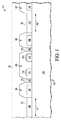
図1が、結合物質121を用いてキャップウェハ105に結合されたデバイスウェハ102を含む、製造されたウェハ101の部分断面側面図を示す。一実施形態において、結合物質121は非導電性グラスフリットである。しかしながら、他の実施形態において、導電性グラスフリット(例えば、鉛のような導電性材料)または半田のような結合材料等のほかの種類の結合物質が用いられてもよい。一実施形態において、複数のウェハは、所定期間に温度や圧力の下で互いに結合されて、2つのウェハとの間に機械的な固相結合を備える。一実施形態において、結合は密封結合(hermetic bond)である。
FIG. 1 shows a partial cross-sectional side view of a manufactured
デバイスウェハ102は、ウェハ102とウェハ105との結合を先立って形成される基板103に配置された複数の半導体デバイス107,109,110を含む。一実施形態において、このデバイスは、半導体製造工程によって形成される半導体、導電性および/または誘電性物質により構成された構造を含む。複数のデバイス107,109,110が、異なる構造を形成するように製造される複数の異なる材料の層を含んでもよい。一実施形態において、複数のデバイス107,109,110は多軸加速度計であるが、他の実施形態において、複数のデバイス107,109,110は、他のタイプの加速度計、センサ、モータまたはスイッチのようなMEMSデバイスであってもよい。また、他の実施形態において、複数のデバイス107、109、110は、集積回路、個別デバイスまたはセンサのような半導体デバイスであってよい。一実施形態において、複数のデバイス107,109,110は、基板103上に異なる層を成形・処理することによって形成される。
The
ウェハ102が、複数のデバイス107,109,110を外部的に外部デバイスに結合する複数のパッド113,115を含んで、外部デバイス(例えば、集積回路ダイ上)に信号を伝達する。複数のパッド113,115は、導電性材料(例えば、銅、アルミニウム、及び金)から形成され、一実施形態において、該導電性材料はワイヤ結合可能である。複数のパッド113,115は、複数のポリシリコン構造114,116上にそれぞれ配置され、複数のポリシリコン構造114,116と電気的にそれぞれ接続される。一実施形態において、基板103が、複数の半導体デバイス107,109,110の導電性構造を複数のパッド支持構造114,116に電気的に結合する複数の導電性構造(図示せず)を含む。例えば、デバイス107は構造114に電気的に結合され、デバイス109は構造116に電気的に結合される。
Wafer 102 includes a plurality of
一実施形態において、基板103が、基板103の層に配置された導電性構造および誘電性構造を有する、シリコン等の半導性材料を含む。いくつかの実施形態において、半導体材料の部分は導電性になるように選択的にドープされる。しかしながら、他の実施形態において、ウェハ102が他の構成を有してもよい。
In one embodiment, the
デバイスウェハ102が、複数のスクライブ領域141,143に配置された部分を含む複数のスクライブ導電性構造108、112を含む。スクライブ領域は、ダイシング中に分離されるウェハの複数のデバイス領域間に配置されるウェハの領域であり、分離経路を含む。複数の構造108,112は、ポリシリコンまたは金属のような導電性材料から形成されている。複数のスクライブ構造108,112の各々は、基板103に配置された導電性構造(図示せず)によって(複数のデバイス107,109,110のうちの)2つのデバイスに電気的に結合される。例えば、導電性構造112は、デバイス109およびデバイス110に電気的に結合される。
The
また、ウェハ102は、デバイスとパッド領域との間に配置される、キャップウェハと結合するための複数の導電性構造124,126を含み、複数のデバイス107,109のシールを提供する。
Wafer 102 also includes a plurality of
一実施形態において、キャップウェハ105は、半導体材料(例えば、シリコン)から形成され、デバイスウェハ102の構造に対するキャビティを形成するための(例えば、エッチングによって形成される)複数の開口131,133,135,137を含む。一実施形態において、ウェハ105はウェハ102に貼り付けられた後、ウェハ105の上面にグラインド加工及びポリッシング加工を行って、ウェハ105の膜厚を薄くする。一実施形態では、ウェハ105は、100〜400マイクロメートルの範囲の薄くされた膜厚に研磨される。しかしながら、他の実施形態において、キャップは他の膜厚に研磨されてもよくまたは研磨しなくてもよい。いくつかの実施形態において、キャップウェハ105が、MEMSデバイスまたはそれに形成される他の半導体デバイスのようなデバイスを含んでもよい。一実施形態において、ウェハ105が、複数の開口131,133,135,137を含まない。
In one embodiment, the
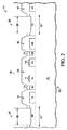
図2は、ウェハ105に複数の開口201,203が形成されてウェハ102のスクライブ領域内の複数の導電性構造108,112を露出させた後に得られるウェハ101の部分的断面側面図を示す。一実施形態において、ウェハ105および結合物質121が複数の構造108,112の上方の位置から除去されて導電性構造を露出させることを保障するために、開口は特定の深さに形成される。このような除去は、複数の構造108,112の上部分を除去することを含んでもよい。一実施形態において、開口は鋸を用いて形成される。図示される実施形態において、複数の開口201,203が80マイクロンの幅205,207を有するが、他の実施形態において、他の幅であってよい。
FIG. 2 shows a partial cross-sectional side view of the
他の実施形態において、結合物質121は、複数の開口201,203の領域に形成されない。この領域において、キャップウェハ105と複数のスクライブ導電性構造108,112との間に空洞がある。しかしながら、この領域に結合物質を形成することは、スクライブ導電性構造108,112とキャップウェハ105との間に結合物質が配置されるため、開口の平らな側壁を提供する。平らな側壁が側壁により優れた導電性層を後に形成する。
In other embodiments, the
他の実施形態において、複数の開口201,203は、両軸円鋸盤、レーザまたはエッチングのような方法によって形成されてもよい。
図3が、ウェハ101上に導電性層301を形成した後に得られるウェハ101の部分的断面図を示す。一実施形態において、層301は金属(例えば、銅、アルミニウム、または金)によって形成される。一実施形態において、層が2マイクロンの膜厚を有するが、他の実施形態において、他の膜厚を有してもよい。優れた電気導電性を備えるために、層301は、複数の開口201,203の側壁に良好なステップカバレッジ(step coverage)を有するように形成される。一実施形態において、層301は、化学蒸着、物理蒸着、電気メッキまたは他の金属形成工程のような金属堆積工程によって形成される。一実施形態において、層301が異なる材料の複数の層を含んでもよい。
In other embodiments, the plurality of
FIG. 3 shows a partial cross-sectional view of the
図4は、複数のパッド113,115の上方に開口401が形成されて後のテストのためにパッドを露出させた後に得られるウェハ101の部分的断面図を示す。一実施形態において、開口401は両軸円鋸盤によって形成されるが、他の実施形態では他の方法(例えば、エッチング)によって形成されてもよい。開口を形成した後に、ウェハ101は、アッシングのような洗浄工程を受けて不要な有機物質を除去する。その後に、複数のデバイス107,109,110は、露出された複数のパッド113,115に接触するテストプローブを用いて動作性をテストされる。
FIG. 4 shows a partial cross-sectional view of the
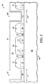
図5は、製造されたウェハ101が別個のダイ529,521,523,527に個体化した後の後部分的断面図を示す。一実施形態において、個体化は、スクライブ領域141,143及びパッド114,116間においてウェハ101を切削することによって実施される。一実施形態において、ウェハは、鋸、レーザまたは他のウェハカット用装置によって切断される。他の実施形態において、個体化は、スクライブ領域においてウェハ101をエッチングすることによって実施することができる。各ダイ529,521,523,527が、(複数の開口131,135,137から形成される)キャビティに配置される半導体デバイス107,109,110を含む。一実施形態において、ウェハ102がウェハ105に結合するとき、このキャビティは密封される。
FIG. 5 shows a rear partial cross-sectional view after the manufactured
図示される実施形態において、複数の鋸経路501,503,515は、40〜50マイクロン幅である幅507,509,511を有するが、他の実施形態において、他の幅であってよい。鋸経路の幅507,509,511は、前に形成された開口201,203の幅205,207未満である。したがって、層301の一部分が開口201,203の側面に残って、各ダイのウェハ105の部分を個体化後に残った導電性スクライブ構造108,112に電気的に結合する導電性経路を提供する。
In the illustrated embodiment, the plurality of
図示される実施形態において、スクライブ導電性構造112,108の残留部分は、構造124,126のような導電性構造に沿ってシールリングを形成して、各ダイのキャビティをシールする。
In the illustrated embodiment, the remaining portions of the scribe
図6は、個体化後のダイ523の上面図を示す。図示される実施形態において、層301は、複数のパッド115,605,607を露出させる開口401によって形成される部分を除いてダイ523の上部のすべてを覆う。図示される実施形態において、層301が、スクライブ領域の上方の開口(例えば、201および203)によって形成される3つの側壁541,603,601を覆う。これにより、図示される実施形態において、2つのウェハ部分を互いに接続する比較的多くの導電性物質が設けられている。他の実施形態において、層301の形状および被覆は異なってよい。例えば、キャップウェハ構造の側壁部分のみまたはキャップウェハ構造のすべての4つの側壁を覆ってもよい。また、他の外部導体のために、層301の上側に開口があってもよい。
FIG. 6 shows a top view of the
製造されたダイは、自身または他の集積回路ダイによって(例えば、密封物質において)さらにパッケージ化されてもよい。層301はパッケージの接地端子に電気的に結合されてもよい。製造されたパッケージは様々な電子システムに利用され得る。
The manufactured die may be further packaged by itself or other integrated circuit die (eg, in a sealing material).
結合された2つのウェハ間の電気的な結合を提供することは、スクライブ領域に開口を形成して、次に開口を被覆する導電性層を形成することを含み、他の従来技術よりも、2つのウェハ間のより効率的および高信頼性の電気的な結合を提供する。2つのウェハの電気的な結合は、電気的に導電性層により形成されるので、電気導電性特徴に関わらず、ウェハの結合物質121は、ウェハの結合物質121の結合特性によって選択され得る。
Providing electrical coupling between two bonded wafers includes forming an opening in the scribe region and then forming a conductive layer covering the opening, over other prior art techniques, Provide more efficient and reliable electrical coupling between two wafers. Since the electrical coupling of the two wafers is formed by an electrically conductive layer, the
このような実施形態において、ワイヤ結合は2つのウェハ間の接地結合に必要とされない。これにより、通常キャップウェハを接地するワイヤボンドはキャップウェハの上面に形成される点で、最終的なパッケージの総計の高さは低くなる。 In such embodiments, wire bonding is not required for ground bonding between the two wafers. As a result, the wire bond that normally grounds the cap wafer is formed on the upper surface of the cap wafer, and the total height of the final package is reduced.
さらに、比較的大きな開口の側壁に導電性層を形成することは、キャップウェハ内に比較的小さな開口に貫挿される導電性ビアを形成することと比べて技術的に容易である。また、層301は、ダイを囲まれるスクライブ領域の大部分を覆うように構成され、内部デバイス領域はワイヤ結合またはビア形成と同様に必要ではない。さらに、複数のワイヤ結合および導電性ビアは、複数のウェハを電気的に結合するために、キャップウェハ構造の側壁に配置される同量の導電性物質を得ることを必要とする。
Furthermore, forming a conductive layer on the sidewall of a relatively large opening is technically easier than forming a conductive via in the cap wafer that penetrates the relatively small opening. Also, the
他の実施形態において、複数の初期スクライブ開口201,203はデバイスウェハ102の下部により形成されて、キャップウェハ105の導電性表面を露出させる。次に、導電性層301は、デバイスウェハ102の底面上に形成され、開口を広げて、キャップウェハ105の露出された導電性表面と接続する。このような実施形態において、デバイスウェハ102の底部は研磨されてウェハ結合後の膜厚を薄くさせる。
In other embodiments, a plurality of
本発明の一実施形態は、第1ウェハを第2ウェハに電気的に結合することを含む。この方法は、第1ウェハを第2ウェハに結合すること、第2ウェハのスクライブ領域内における第1ウェハに開口を形成して第2ウェハの導電性構造の表面を露出させること、導電性層が第2ウェハの導電性構造と電気的に接続部を形成するように第1ウェハおよび第1ウェハにおける開口上に導電性層を形成して第1ウェハを第2ウェハに電気的に結合することを含む。 One embodiment of the present invention includes electrically coupling a first wafer to a second wafer. The method includes bonding a first wafer to a second wafer, forming an opening in the first wafer in a scribe region of the second wafer to expose a surface of the conductive structure of the second wafer, a conductive layer Electrically connecting the first wafer to the second wafer by forming a conductive layer over the openings in the first wafer and the first wafer so as to form an electrical connection with the conductive structure of the second wafer. Including that.
別の実施形態が、キャップウェハをデバイスウェハに電気的に結合する方法を含む。該方法は、結合物質を用いてキャップウェハをデバイスウェハに結合することを含む。デバイスウェハは、基板を含む。該方法は、デバイスウェハのスクライブ領域に結合物質を形成し、且つキャップウェハに開口を形成して、デバイスウェハの導電性構造の表面を露出させることを含む。キャップウェハおよび結合材料を貫通する開口を形成することは、デバイスウェハのスクライブ領域におけるキャップウェハ及び結合物質を切削することを含む。該方法は、導電性層がデバイスウェハの導電性構造と電気的接続を形成するようにキャップウェハおよびキャップウェハにおける開口上に導電性層を形成して、キャップウェハをデバイスウェハに電気的に結合することを含む。 Another embodiment includes a method of electrically coupling a cap wafer to a device wafer. The method includes bonding a cap wafer to a device wafer using a bonding material. The device wafer includes a substrate. The method includes forming a binding material in a scribe region of the device wafer and forming an opening in the cap wafer to expose a surface of the conductive structure of the device wafer. Forming the opening through the cap wafer and bonding material includes cutting the cap wafer and bonding material in a scribe region of the device wafer. The method electrically couples the cap wafer to the device wafer by forming a conductive layer over the cap wafer and the opening in the cap wafer such that the conductive layer forms an electrical connection with the conductive structure of the device wafer. Including doing.
別の実施形態が、第1ウェハを第2ウェハに電気的に結合する方法を含む。該方法は、結合物質を用いて第1ウェハを第2ウェハに結合すること、第2ウェハのスクライブ領域に結合物質を形成し、且つ第1ウェハに開口を形成して、第2ウェハの導電性構造の表面を露出させること、および導電性層が第2ウェハの導電性構造と電気的接続部を形成するように第1ウェハ及び第1ウェハにおける開口上に導電性層を形成して、第1ウェハを第2ウェハに電気的に結合することを含む。該方法は、結合ウェハを複数のダイに分離することを含む。分離することは、第2ウェハの分離経路の物質を除去し、分離経路は第1幅を有する。開口が第2幅を有し、導電性層の少なくとも1つの部分が、分離されたダイの少なくとも1つの側壁に残るように、第1および第2幅を選択して、第1ウェハと第2ウェハとの間の電気的結合を提供する。 Another embodiment includes a method of electrically coupling a first wafer to a second wafer. The method includes bonding a first wafer to a second wafer using a bonding material, forming a bonding material in a scribe region of the second wafer, and forming an opening in the first wafer to conduct the second wafer. Exposing the surface of the conductive structure and forming a conductive layer over the opening in the first wafer and the first wafer such that the conductive layer forms an electrical connection with the conductive structure of the second wafer; Electrically coupling the first wafer to the second wafer. The method includes separating the bonded wafer into a plurality of dies. Separating removes material in the separation path of the second wafer, and the separation path has a first width. The first and second widths are selected such that the opening has a second width and at least one portion of the conductive layer remains on at least one sidewall of the separated die. Provides electrical coupling to the wafer.
本発明の特定の実施態様を示して説明してきたが、本明細書の教示に基づいて、本発明およびそのより広範な態様から逸脱することなく、さらなる変更および修正がなされ得ることが当業者には認められるであろう。したがって添付の特許請求の範囲は、本発明の真の精神および範囲の内にあるそのような変更および修正の全てを、その範囲の内に包含するものである。 While particular embodiments of the present invention have been shown and described, it will be apparent to those skilled in the art that further changes and modifications may be made based on the teachings herein without departing from the invention and its broader aspects. Will be accepted. Accordingly, the appended claims are to encompass within their scope all such changes and modifications as fall within the true spirit and scope of this invention.
Claims (6)
結合物質を用いて前記第1ウェハを前記第2ウェハに結合して、結合されたウェハを形成すること、
前記第1ウェハと前記第2ウェハのスクライブ領域における結合物質とに開口を形成して前記第2ウェハの導電性構造の少なくとも一部分を露出させること、
前記第1ウェハおよび前記第1ウェハにおける前記開口上に導電性層を形成して、前記導電性層が前記第2ウェハの導電性構造との電気的接続を形成して前記第1ウェハを前記第2ウェハに電気的に結合すること、
前記結合されたウェハを複数のダイに分離することを備え、
前記分離することは、前記第2ウェハの分離経路の物質を除去することを含み、
前記分離経路は、第1幅を有し、前記開口は第2幅を有し、
前記第1幅および前記第2幅は、分離されたダイの少なくとも1つの側壁に前記導電性層の少なくとも1つの部分を残して、前記第1ウェハと前記第2ウェハとの間の電気的結合を提供するように選択される、方法。 A method of electrically coupling a first wafer to a second wafer, comprising:
Bonding the first wafer to the second wafer using a bonding material to form a bonded wafer;
Forming an opening in the binding material in the scribe region of the first wafer and the second wafer to expose at least a portion of the conductive structure of the second wafer ;
Forming a conductive layer over the opening in the first wafer and the first wafer, the conductive layer forming an electrical connection with a conductive structure of the second wafer, and Electrically coupling to the second wafer;
Separating the bonded wafers into a plurality of dies,
The separating includes removing material of a separation path of the second wafer;
The separation path has a first width and the opening has a second width;
The first width and the second width are electrically coupled between the first wafer and the second wafer, leaving at least one portion of the conductive layer on at least one sidewall of a separated die. Selected to provide a method.
前記第1ウェハにおいて前記開口を形成した後に、前記第1ウェハに第2開口を形成して前記複数のパッドの露出させることをさらに備える、請求項1に記載の方法。 The second wafer includes a plurality of pads;
The method of claim 1, further comprising forming a second opening in the first wafer to expose the plurality of pads after forming the opening in the first wafer.
前記結合物質は、前記第2ウェハのスクライブ領域において前記第2ウェハの導電性構造の上方に位置する、請求項1に記載の方法。 The method of claim 1, wherein the binding material is located above the conductive structure of the second wafer in a scribe region of the second wafer.
Applications Claiming Priority (3)
| Application Number | Priority Date | Filing Date | Title |
|---|---|---|---|
| US12/638,424 US8138062B2 (en) | 2009-12-15 | 2009-12-15 | Electrical coupling of wafer structures |
| US12/638,424 | 2009-12-15 | ||
| PCT/US2010/057624 WO2011081741A2 (en) | 2009-12-15 | 2010-11-22 | Electrical coupling of wafer structures |
Publications (3)
| Publication Number | Publication Date |
|---|---|
| JP2013513971A JP2013513971A (en) | 2013-04-22 |
| JP2013513971A5 JP2013513971A5 (en) | 2014-01-16 |
| JP5721742B2 true JP5721742B2 (en) | 2015-05-20 |
Family
ID=44143393
Family Applications (1)
| Application Number | Title | Priority Date | Filing Date |
|---|---|---|---|
| JP2012544551A Expired - Fee Related JP5721742B2 (en) | 2009-12-15 | 2010-11-22 | Electrical coupling of wafer structures |
Country Status (5)
| Country | Link |
|---|---|
| US (1) | US8138062B2 (en) |
| JP (1) | JP5721742B2 (en) |
| CN (1) | CN102656673B (en) |
| TW (1) | TWI555069B (en) |
| WO (1) | WO2011081741A2 (en) |
Families Citing this family (8)
| Publication number | Priority date | Publication date | Assignee | Title |
|---|---|---|---|---|
| US8637981B2 (en) | 2011-03-30 | 2014-01-28 | International Rectifier Corporation | Dual compartment semiconductor package with temperature sensor |
| US8633088B2 (en) | 2012-04-30 | 2014-01-21 | Freescale Semiconductor, Inc. | Glass frit wafer bond protective structure |
| US9266717B2 (en) | 2013-03-15 | 2016-02-23 | Versana Micro Inc | Monolithically integrated multi-sensor device on a semiconductor substrate and method therefor |
| CN103466541B (en) * | 2013-09-12 | 2016-01-27 | 上海矽睿科技有限公司 | Wafer-level packaging method and wafer |
| US9630832B2 (en) * | 2013-12-19 | 2017-04-25 | Taiwan Semiconductor Manufacturing Company, Ltd. | Semiconductor device and method of manufacturing |
| US9826630B2 (en) | 2014-09-04 | 2017-11-21 | Nxp Usa, Inc. | Fan-out wafer level packages having preformed embedded ground plane connections and methods for the fabrication thereof |
| KR20180032985A (en) * | 2016-09-23 | 2018-04-02 | 삼성전자주식회사 | Integrated circuit package and method of manufacturing the same and wearable device including integrated circuit package |
| CN107827079B (en) * | 2017-11-17 | 2019-09-20 | 烟台睿创微纳技术股份有限公司 | A kind of production method of MEMS chip |
Family Cites Families (14)
| Publication number | Priority date | Publication date | Assignee | Title |
|---|---|---|---|---|
| JP3613838B2 (en) | 1995-05-18 | 2005-01-26 | 株式会社デンソー | Manufacturing method of semiconductor device |
| US6762072B2 (en) * | 2002-03-06 | 2004-07-13 | Robert Bosch Gmbh | SI wafer-cap wafer bonding method using local laser energy, device produced by the method, and system used in the method |
| SG111972A1 (en) | 2002-10-17 | 2005-06-29 | Agency Science Tech & Res | Wafer-level package for micro-electro-mechanical systems |
| JP3905041B2 (en) * | 2003-01-07 | 2007-04-18 | 株式会社日立製作所 | Electronic device and manufacturing method thereof |
| US20040166662A1 (en) | 2003-02-21 | 2004-08-26 | Aptos Corporation | MEMS wafer level chip scale package |
| JP4551638B2 (en) * | 2003-08-01 | 2010-09-29 | 富士フイルム株式会社 | Method for manufacturing solid-state imaging device |
| DE10350460B4 (en) * | 2003-10-29 | 2006-07-13 | X-Fab Semiconductor Foundries Ag | Method for producing semiconductor devices having micromechanical and / or microelectronic structures, which result from the fixed connection of at least two semiconductor wafers, and corresponding arrangement |
| US7034393B2 (en) | 2003-12-15 | 2006-04-25 | Analog Devices, Inc. | Semiconductor assembly with conductive rim and method of producing the same |
| TWI236111B (en) * | 2004-06-30 | 2005-07-11 | Ind Tech Res Inst | Apparatus and method for wafer level packaging |
| US7495462B2 (en) | 2005-03-24 | 2009-02-24 | Memsic, Inc. | Method of wafer-level packaging using low-aspect ratio through-wafer holes |
| TWI295081B (en) * | 2006-01-12 | 2008-03-21 | Touch Micro System Tech | Method for wafer level package and fabricating cap structures |
| US20080131662A1 (en) * | 2006-12-05 | 2008-06-05 | Jordan Larry L | Alignment of a cap to a MEMS wafer |
| US20080191334A1 (en) | 2007-02-12 | 2008-08-14 | Visera Technologies Company Limited | Glass dam structures for imaging devices chip scale package |
| US20080290430A1 (en) * | 2007-05-25 | 2008-11-27 | Freescale Semiconductor, Inc. | Stress-Isolated MEMS Device and Method Therefor |
-
2009
- 2009-12-15 US US12/638,424 patent/US8138062B2/en not_active Expired - Fee Related
-
2010
- 2010-11-22 CN CN201080056932.8A patent/CN102656673B/en not_active Expired - Fee Related
- 2010-11-22 WO PCT/US2010/057624 patent/WO2011081741A2/en active Application Filing
- 2010-11-22 JP JP2012544551A patent/JP5721742B2/en not_active Expired - Fee Related
- 2010-12-06 TW TW099142440A patent/TWI555069B/en not_active IP Right Cessation
Also Published As
| Publication number | Publication date |
|---|---|
| TWI555069B (en) | 2016-10-21 |
| JP2013513971A (en) | 2013-04-22 |
| US20110143476A1 (en) | 2011-06-16 |
| CN102656673A (en) | 2012-09-05 |
| TW201128691A (en) | 2011-08-16 |
| US8138062B2 (en) | 2012-03-20 |
| WO2011081741A2 (en) | 2011-07-07 |
| WO2011081741A3 (en) | 2011-09-09 |
| CN102656673B (en) | 2015-05-20 |
Similar Documents
| Publication | Publication Date | Title |
|---|---|---|
| JP5721742B2 (en) | Electrical coupling of wafer structures | |
| EP2727136B1 (en) | Process for a sealed mems device with a portion exposed to the environment | |
| US9362139B2 (en) | Method of making a semiconductor device having a functional capping | |
| TWI619669B (en) | Process to produce a hybrid integrated and hybrid integrated component with at least two mems-parts | |
| CN102569194B (en) | Protecting T-contacts of chip scale packages from moisture | |
| TWI628784B (en) | Stress released image sensor package structure and method | |
| CN104716050B (en) | Semiconductor devices with molding through hole | |
| EP1070677A2 (en) | Microcap wafer-level package | |
| US20120108055A1 (en) | Manufacturing process of semiconductor device and semiconductor device | |
| US9972554B2 (en) | Wafer level chip scale package having continuous through hole via configuration and fabrication method thereof | |
| US8252695B2 (en) | Method for manufacturing a micro-electromechanical structure | |
| CN108083224B (en) | MEMS component with low-resistance wiring and method for producing such a MEMS component | |
| US9919915B2 (en) | Method and system for MEMS devices with dual damascene formed electrodes | |
| CN211004545U (en) | MEMS chip with TSV structure | |
| CN107697882B (en) | Process for manufacturing a semiconductor device and corresponding semiconductor device | |
| US7911043B2 (en) | Wafer level device package with sealing line having electroconductive pattern and method of packaging the same | |
| TWI540616B (en) | Wafer level array of chips and method thereof | |
| CN110713165A (en) | MEMS chip with TSV structure and wafer-level air tightness packaging method thereof | |
| CN102084479A (en) | Wafer level integration module with interconnects | |
| CN112366131B (en) | Method for manufacturing semiconductor device | |
| US20080283989A1 (en) | Wafer level package and wafer level packaging method | |
| EP1199744A1 (en) | Microcap wafer-level package | |
| CN115215290A (en) | MEMS device wafer level packaging method and MEMS device | |
| CN108417591B (en) | High-electrical-property chip packaging structure and manufacturing method | |
| US7985697B2 (en) | Wafer level package and method of fabricating the same |
Legal Events
| Date | Code | Title | Description |
|---|---|---|---|
| A521 | Request for written amendment filed |
Free format text: JAPANESE INTERMEDIATE CODE: A523 Effective date: 20131121 |
|
| A621 | Written request for application examination |
Free format text: JAPANESE INTERMEDIATE CODE: A621 Effective date: 20131121 |
|
| A977 | Report on retrieval |
Free format text: JAPANESE INTERMEDIATE CODE: A971007 Effective date: 20140428 |
|
| A131 | Notification of reasons for refusal |
Free format text: JAPANESE INTERMEDIATE CODE: A131 Effective date: 20140527 |
|
| A601 | Written request for extension of time |
Free format text: JAPANESE INTERMEDIATE CODE: A601 Effective date: 20140827 |
|
| A602 | Written permission of extension of time |
Free format text: JAPANESE INTERMEDIATE CODE: A602 Effective date: 20140903 |
|
| A521 | Request for written amendment filed |
Free format text: JAPANESE INTERMEDIATE CODE: A523 Effective date: 20140926 |
|
| TRDD | Decision of grant or rejection written | ||
| A01 | Written decision to grant a patent or to grant a registration (utility model) |
Free format text: JAPANESE INTERMEDIATE CODE: A01 Effective date: 20150224 |
|
| A61 | First payment of annual fees (during grant procedure) |
Free format text: JAPANESE INTERMEDIATE CODE: A61 Effective date: 20150324 |
|
| R150 | Certificate of patent or registration of utility model |
Ref document number: 5721742 Country of ref document: JP Free format text: JAPANESE INTERMEDIATE CODE: R150 |
|
| LAPS | Cancellation because of no payment of annual fees |