JP5697353B2 - Image processing apparatus, image processing apparatus control method, and program - Google Patents
Image processing apparatus, image processing apparatus control method, and program Download PDFInfo
- Publication number
- JP5697353B2 JP5697353B2 JP2010073472A JP2010073472A JP5697353B2 JP 5697353 B2 JP5697353 B2 JP 5697353B2 JP 2010073472 A JP2010073472 A JP 2010073472A JP 2010073472 A JP2010073472 A JP 2010073472A JP 5697353 B2 JP5697353 B2 JP 5697353B2
- Authority
- JP
- Japan
- Prior art keywords
- value
- pixel
- circuit
- signal
- determination
- Prior art date
- Legal status (The legal status is an assumption and is not a legal conclusion. Google has not performed a legal analysis and makes no representation as to the accuracy of the status listed.)
- Active
Links
Images


Classifications
-
- H—ELECTRICITY
- H04—ELECTRIC COMMUNICATION TECHNIQUE
- H04N—PICTORIAL COMMUNICATION, e.g. TELEVISION
- H04N25/00—Circuitry of solid-state image sensors [SSIS]; Control thereof
- H04N25/60—Noise processing, e.g. detecting, correcting, reducing or removing noise
- H04N25/68—Noise processing, e.g. detecting, correcting, reducing or removing noise applied to defects
- H04N25/683—Noise processing, e.g. detecting, correcting, reducing or removing noise applied to defects by defect estimation performed on the scene signal, e.g. real time or on the fly detection
Description
本発明は、撮像素子の欠陥画素の信号を検出する画像処理装置、画像処理装置の制御方法及びプログラムに関する。 The present invention relates to an image processing apparatus that detects a signal of a defective pixel of an image sensor, a control method for the image processing apparatus, and a program.
デジタルカメラやデジタルビデオカメラなどの撮像装置では、カラーフィルタを配置した撮像素子として、一般的に、CCDセンサやCMOSセンサなどが使用されている。このような撮像素子では、構造上の要因、製造過程における要因、製造後の外的な要因などによって、欠陥画素(「点滅傷」とも呼ばれる)が発生することがある。例えば、CMOSセンサにおいて欠陥画素が発生する要因の1つとして、フォトダイオードから電荷を受けるフローティング・ディフュージョンで生じるノイズが挙げられる。かかるノイズは、周期的に発生するとは限らず、数回の撮像に1回と高頻度で発生する場合もあるし、数年に1回と低頻度で発生する場合もある。また、撮像素子の欠陥画素の発生頻度は、温度や電荷の蓄積時間に依存しないことがわかっている。 In an imaging apparatus such as a digital camera or a digital video camera, a CCD sensor, a CMOS sensor, or the like is generally used as an imaging element having a color filter. In such an image sensor, defective pixels (also referred to as “flashing scratches”) may occur due to structural factors, manufacturing process factors, external factors after manufacturing, and the like. For example, one of the factors that cause defective pixels in a CMOS sensor is noise generated by floating diffusion that receives charges from a photodiode. Such noise does not necessarily occur periodically, and may occur as frequently as once in several imaging operations, or may occur as infrequently as once in several years. Further, it has been found that the frequency of occurrence of defective pixels in the image sensor does not depend on the temperature or the charge accumulation time.
そこで、撮像素子の欠陥画素を検出する技術が幾つか提案されている(特許文献1及び2参照)。これらの技術は、製造過程において特定の位置に発生した欠陥画素に限らず、製造後において発生した欠陥画素も検出することができる。例えば、特許文献1には、注目画素と、注目画素の周辺の複数の画素との信号レベルの差分をカラーフィルタの色ごとに求め、全ての差分が閾値以上である場合に注目画素を欠陥画素として検出する技術が開示されている。また、特許文献2には、カラーフィルタの色を区別することなく全ての画素の輝度値を求め、注目画素と周辺の複数の画素との輝度レベルの差が閾値以上である場合に注目画素を欠陥画素として検出する技術が開示されている。
Therefore, several techniques for detecting defective pixels of the image sensor have been proposed (see
しかしながら、従来技術では、撮像素子に発生する欠陥画素を高精度に検出することができなかった。例えば、特許文献1に開示された技術では、高感度撮像を行った場合、画像データ(画像信号)の増幅率が大きくなるため、画像データに含まれているノイズ成分も増幅され、注目画素の周囲の画素の信号レベルに比べて目立ってしまうことがある。特に、被写体の空間周波数が低域となる領域では、このノイズ成分が周囲の画素の信号レベルよりも大きな値となる可能性が高く、その結果、周囲の画素との信号レベルの差分が閾値よりも大きくなり、注目画素を欠陥画素と誤検出してしまうことになる。なお、このような誤検出を回避するために閾値を高く設定することも考えられるが、信号レベルが高い領域では、注目画素と周囲の画素との信号レベルの差分が小さくなる(現れにくくなる)ため、欠陥画素を検出することができなくなってしまう。また、特許文献2に開示された技術においても、特許文献1と同様な課題が生じてしまう。
However, in the prior art, defective pixels generated in the image sensor cannot be detected with high accuracy. For example, in the technique disclosed in
本発明は、このような従来技術の課題に鑑みてなされ、撮像素子の欠陥画素を高精度に検出することができる技術を提供することを例示的目的とする。 The present invention has been made in view of the problems of the conventional technology, and an object of the present invention is to provide a technology capable of detecting a defective pixel of an image sensor with high accuracy.
上記目的を達成するために、本発明の一側面としての画像処理装置は、複数の画素で構成された撮像素子で生成された画像データから、前記撮像素子の欠陥画素の信号を検出する画像処理装置であって、注目画素の周囲に位置する複数の画素の信号レベルに対する、前記注目画素の信号レベルの差分の大きさを示す第1の判定値を求める第1の判定手段と、前記注目画素の周囲に位置する複数の画素の信号レベルに対する、前記注目画素の信号レベルの差分の大きさのばらつきを示す第2の判定値を求める第2の判定手段と、前記第1の判定値及び前記第2の判定値を用いて、前記注目画素の信号が欠陥画素の信号であるか否かを検出する検出手段と、を有し、前記第1の判定手段は、前記注目画素の周囲に位置する複数の画素のそれぞれの信号レベルについて、前記注目画素の信号レベルとの差分を求め、それぞれの差分から前記注目画素の信号が欠陥画素の信号である可能性を示す値を求め、求めた値を乗算することで前記第1の判定値を求めることを特徴とする。 In order to achieve the above object, an image processing apparatus according to an aspect of the present invention detects image signals of defective pixels of an image sensor from image data generated by an image sensor composed of a plurality of pixels. A first determination unit for obtaining a first determination value indicating a difference in signal level of the pixel of interest with respect to signal levels of a plurality of pixels located around the pixel of interest; Second determination means for obtaining a second determination value indicating a variation in the difference in the signal level of the target pixel with respect to the signal levels of a plurality of pixels located around the pixel, the first determination value, and the Detecting means for detecting whether or not the signal of the target pixel is a signal of a defective pixel using a second determination value, and the first determination means is located around the target pixel. Each of a plurality of pixels For the signal level, a difference from the signal level of the target pixel is obtained, a value indicating the possibility that the signal of the target pixel is a defective pixel signal is obtained from each difference, and the obtained value is multiplied by the obtained value. The determination value of 1 is obtained .
また、上記目的を達成するために、本発明の別の一側面としての画像処理装置は、複数の画素で構成された撮像素子で生成された画像データから、前記撮像素子の欠陥画素の信号を検出する画像処理装置であって、注目画素の周囲に位置する複数の画素の信号レベルに対する、前記注目画素の信号レベルの差分の大きさを示す第1の判定値を求める第1の判定手段と、前記注目画素の周囲に位置する複数の画素の信号レベルに対する、前記注目画素の信号レベルの差分の大きさのばらつきを示す第2の判定値を求める第2の判定手段と、前記第1の判定値と前記第2の判定値を乗算して得られた値を用いて、前記注目画素の信号レベルと、前記注目画素の周囲に位置する画素の信号レベルから求めた補正値を重み付け加算することで、前記注目画素の信号レベルを補正する補正手段と、を有し、前記第1の判定値は前記差分の大きさが大きいほど大きな値となり、前記第2の判定値は前記差分の大きさのばらつきが小さいほど大きな値となるものであって、前記補正手段は、前記第1の判定値と前記第2の判定値を乗算して得られた値が大きいほど、前記補正値の重み付けを大きくすることを特徴とする。 In order to achieve the above object, an image processing apparatus according to another aspect of the present invention receives a signal of a defective pixel of the image sensor from image data generated by an image sensor composed of a plurality of pixels. An image processing apparatus for detecting, wherein the first determination means obtains a first determination value indicating a magnitude of a difference in signal level of the target pixel with respect to signal levels of a plurality of pixels located around the target pixel; , Second determination means for obtaining a second determination value indicating a variation in the magnitude of the difference in signal level of the pixel of interest with respect to the signal levels of a plurality of pixels located around the pixel of interest; Using a value obtained by multiplying the determination value by the second determination value, weighting addition is performed on the signal level of the target pixel and the correction value obtained from the signal level of the pixels located around the target pixel. In the above note Correction means for correcting a signal level of a pixel, wherein the first determination value becomes larger as the difference is larger, and the second determination value has less variation in the difference. The correction means increases the weight of the correction value as the value obtained by multiplying the first determination value and the second determination value increases. Features.
本発明の更なる目的又はその他の側面は、以下、添付図面を参照して説明される好ましい実施形態によって明らかにされるであろう。 Further objects and other aspects of the present invention will become apparent from the preferred embodiments described below with reference to the accompanying drawings.
本発明によれば、例えば、撮像素子の欠陥画素を高精度に検出する技術を提供することができる。 ADVANTAGE OF THE INVENTION According to this invention, the technique which detects the defective pixel of an image pick-up element with high precision can be provided, for example.
以下、添付図面を参照して、本発明の好適な実施の形態について説明する。なお、各図において、同一の部材については同一の参照番号を付し、重複する説明は省略する。 DESCRIPTION OF EXEMPLARY EMBODIMENTS Hereinafter, preferred embodiments of the invention will be described with reference to the accompanying drawings. In addition, in each figure, the same reference number is attached | subjected about the same member and the overlapping description is abbreviate | omitted.
図1は、本発明の一側面としての画像処理装置が適用された撮像装置100の構成を示す概略ブロック図である。撮像装置100は、被写体を撮像する撮像装置であって、本実施形態では、デジタルカメラとして具現化される。
FIG. 1 is a schematic block diagram illustrating a configuration of an
撮像装置100は、撮像レンズ101と、絞り102と、R(赤)、G(緑)、B(青)のカラーフィルタが配置された撮像素子103と、撮像素子103からのアナログの画像信号(電気信号)をデジタルの画像データに変換するA/D変換回路104を有する。また、撮像装置100は、撮像素子103の欠陥画素(点滅傷など)の信号を検出する画像処理装置として機能する欠陥画素検出回路105を有する。また、撮像装置100は、欠陥画素検出回路105によって欠陥画素から出力されたものとして検出された信号に対して補正を行う欠陥画素補正回路106を有する。また、撮像装置100は、各回路のバスアービトレーションを行うメモリ制御回路107と、画像データを一時的に記憶するDRAM108と、色変換処理やシャープネス処理などの画像処理を行う画像処理回路109を有する。また、撮像装置100は、画像データの縮小や拡大を行う変倍回路110と、各回路のモードやパラメータを決定するシステムコントローラ111と、画像データに対応する画像を表示(再生)する表示部112を有する。また、撮像装置100は、表示部112に画像を表示するために画像信号を変調するビデオ変調回路113と、画像データを圧縮処理する圧縮回路114を有する。また、撮像装置100は、圧縮回路114によって圧縮された画像データを記録する着脱可能な記録媒体115と、記録媒体115とのインターフェースとして機能する媒体制御回路116を有する。
The
撮像レンズ101に入射した光(被写体光)は、絞り102を通過して適正に露出された状態で撮像素子103に入射し、撮像素子103によって電気信号に変換される。撮像素子103で生成された被写体光の電気信号は、A/D変換回路104によってアナログ画像信号からデジタル画像データに変換される。
Light (subject light) that has entered the
撮像素子103及びA/D変換回路104で生成され、複数の画素から出力された信号で構成された画像データは、欠陥画素検出回路105において、画像データの中に含まれる欠陥画素の信号が検出される。欠陥画素検出回路105によって欠陥画素から出力されたものとして検出された信号は、欠陥画素補正回路106において、欠陥画素として検出された画素の周囲に位置する画素の信号を参照した補間により補正される。
Image data generated by the
欠陥画素補正回路106によって欠陥画素から出力されたものとして検出された信号が補正された画像データは、メモリ制御回路107を介して、DRAM108に書き込まれる。そして、DRAM108に書き込まれた画像データは、メモリ制御回路107を介して、画像処理回路109に読み出される。
Image data obtained by correcting the signal detected as being output from the defective pixel by the defective
画像処理回路109では、色変換処理やシャープネス処理などが行われ、DRAM108から読み出された画像データは、輝度信号と色差信号とを含む画像データに変換される。画像処理回路109によって処理された画像データは、メモリ制御回路107を介して、DRAM108に書き込まれる。そして、DRAM108に書き込まれた画像データは、メモリ制御回路107を介して、変倍回路110に読み出される。
The
変倍回路110は、画像データに対応する画像を表示部112に表示するために、例えば、720×240のサイズに画像データを変倍する。変倍回路110で変倍された画像データは、メモリ制御回路107を介して、DRAM108に書き込まれる。そして、DRAM108に書き込まれた画像データは、メモリ制御回路107を介して、ビデオ変調回路113に読み出される。
The
ビデオ変調回路113では、画像データのエンコードが行われる。画像処理回路109によって処理された画像データは、表示部112において、画像として表示される。
The
また、画像データを記録媒体115に書き込む場合には、変倍回路110は、DRAM108から読み出された画像データ(画像処理回路109によって処理され、DRAM108に書き込まれた後で読み出された画像データ)を所定のサイズに変倍する。変倍回路110で変倍された画像データは、メモリ制御回路107を介して、DRAM108に書き込まれる。そして、DRAM108に書き込まれた画像データは、メモリ制御回路107を介して、圧縮回路114に読み出される。
In addition, when writing image data to the
圧縮回路114は、DRAM108から読み出された画像データをJPEG等の圧縮方式で圧縮する。圧縮回路114によって圧縮された画像データは、メモリ制御回路107を介して、DRAM108に書き込まれた後で、媒体制御回路116に読み出される。媒体制御回路116は、圧縮回路114によって圧縮された画像データを記録媒体115に書き込む(記録する)。
The
図2を参照して、撮像素子103及びA/D変換回路104で生成された画像データを用いて、撮像素子103の欠陥画素の信号を検出する欠陥画素検出回路105について詳細に説明する。上述したように、撮像素子103にはベイヤー配列のカラーフィルタが配置されているため、撮像素子103及びA/D変換回路104で生成された画像データは、複数種類(R、G、Bの3種類)の単色画素群から構成されている。なお、本実施形態では、注目画素としてのG画素に欠陥画素(点滅傷)が発生した場合を例に説明する。
With reference to FIG. 2, the defective
欠陥画素検出回路105には、A/D変換回路104から、デジタル化された画像データが入力される。画素データに含まれる各画素の信号レベルは8ビットで示されるものとする。欠陥画素検出回路105は、ゼロ挿入回路201と、第1の低域通過(ローパス)フィルタ(LPF)回路202と、第2のLPF回路203と、第3のLPF回路204と、第4のLPF回路205とを含む。また、欠陥画素検出回路105は、第1の高域通過(ハイパス)フィルタ(HPF)回路206と、第2のHPF回路207と、第3のHPF回路208と、第4のHPF回路209とを含む。また、欠陥画素検出回路105は、第1のアブソリュート(ABS)回路210と、第2のABS回路211と、第3のABS回路212と、第4のABS回路213とを含む。また、欠陥画素検出回路105は、輝度信号生成回路214と、傷判定回路215と、閾値判定回路(第1の判定部)216と、相関判定回路(第2の判定部)217と、乗算器218と、セレクタ219とを含む。
The defective
ゼロ挿入回路201は、図3(a)に示すように、注目画素を中心とする複数の画素で構成される領域において、G画素以外の画素(注目画素と異なる色の画素)の信号レベルにゼロ値(0)を挿入する。
As shown in FIG. 3A, the zero
第1のLPF回路202は、図3(b)に示すように、G画素以外の画素の信号レベルにゼロ値が挿入された画像データに対して、垂直方向についてローパスフィルタ処理((1、2、1)などのフィルタ係数を有する低域通過フィルタ処理)を行う。これにより、ゼロ値の画素の信号レベルが垂直方向の画素の信号レベルで補間される。
As shown in FIG. 3B, the
第2のLPF回路203は、図3(c)に示すように、G画素以外の画素の信号レベルにゼロ値が挿入された画像データに対して、水平方向についてLPF処理を行う。これにより、ゼロ値の画素の信号レベルが水平方向の画素で補間される。
As shown in FIG. 3C, the
第3のLPF回路204は、図3(d)に示すように、G画素以外の画素の信号レベルにゼロ値が挿入された画像データに対して、135度方向についてLPF処理を行う。これにより、ゼロ値の画素の信号レベルが135度方向の画素の信号レベルで補間される。
As shown in FIG. 3D, the
第4のLPF回路205は、図3(e)に示すように、G画素以外の画素の信号レベルにゼロ値が挿入された画像データに対して、45度方向についてLPF処理を行う。これにより、ゼロ値の画素の信号レベルが45度方向の画素の信号レベルで補間される。
As shown in FIG. 3E, the
第1のHPF回路206は、図3(f)に示すように、第1のLPF回路202によるLPF処理の結果(出力データ)に対して、水平方向についてハイパスフィルタ処理((−1、2、−1)などのフィルタ係数を有する高域通過フィルタ処理)を行う。
As shown in FIG. 3 (f), the
第2のHPF回路207は、図3(g)に示すように、第2のLPF回路203によるLPF処理の結果(出力データ)に対して、垂直方向についてHPF処理を行う。
As shown in FIG. 3G, the
第3のHPF回路208は、図3(h)に示すように、第3のLPF回路204によるLPF処理の結果(出力データ)に対して、45度方向についてHPF処理を行う。
As shown in FIG. 3H, the
第4のHPF回路209は、図3(i)に示すように、第4のLPF回路205によるLPF処理の結果(出力データ)に対して、135度方向についてHPF処理を行う。
As shown in FIG. 3I, the
このように、欠陥画素検出回路105において、第1のLPF回路203と第1のHPF回路206とは、注目画素を基準として互いに異なる方向についてフィルタ処理を行う処理部を構成する。同様に、第2のLPF回路203と第2のHPF回路207、第3のLPF回路204と第3のHPF回路208、第4のLPF回路205と第4のHPF回路209もフィルタ処理を行う処理部を構成する。なお、LPF処理の処理方向(第1の方向)及びHPF処理の処理方向(第1の方向に直交する第2の方向)は、処理部のそれぞれで互いに異なる。
As described above, in the defective
第1のABS回路210は、第1のHPF回路206によるHPF処理の結果(出力データ)の絶対値を8ビットで出力する。同様に、第2のABS回路211、第3のABS回路212及び第4のABS回路213のそれぞれは、第2のHPF回路207、第3のHPF回路208及び第4のHPF回路209によるHPF処理の結果(出力データ)の絶対値を8ビットで出力する。第1のHPF回路206乃至第4のHPF回路209によるHPF処理の結果の絶対値を、それぞれHA1、HA2、HA3及びHA4とする。
The
輝度信号生成回路214は、欠陥画素検出回路105に入力される画像データ(R、G、Bのベイヤー配列からなる画像データ)から輝度信号を生成する。例えば、輝度信号生成回路214は、以下の式1に従って、輝度信号Yを生成する。
Y=0.299R+0.587G+0.114B ・・・(式1)
傷判定回路215は、第1のHPF回路206乃至第4のHPF回路209によるHPF処理の結果の符号(正又は負)に応じて、注目画素の信号が欠陥画素の信号であるかどうかを示す傷フラグを出力する。また、傷判定回路215は、欠陥画素が白傷であるか黒傷であるかを示す白黒フラグとを出力する。ここで、白傷とは、暗状態で明るく見える欠陥画素であり、黒傷とは、入射光がある状態で暗く見える欠陥画素である。
The luminance
Y = 0.299R + 0.587G + 0.114B (Formula 1)
The
具体的には、第1のHPF回路206乃至第4のHPF回路209による全てのHPF処理の結果が同じ符号である場合には、傷判定回路215は、傷フラグ(1ビット)として、フラグ「1」を出力する。これは、注目画素の信号が欠陥画素の信号であることを示す。一方、第1のHPF回路206乃至第4のHPF回路209によるHPF処理の結果の符号が1つでも異なる場合には、傷判定回路215は、傷フラグとして、フラグ「0」を出力する。これは、注目画素の信号が欠陥画素の信号でないことを示す。なお、傷フラグは、セレクタ219の選択信号となる。
Specifically, when all the HPF processing results by the
また、第1のHPF回路206乃至第4のHPF回路209による全てのHPF処理の結果が正の符号である場合には、傷判定回路215は、白黒フラグ(1ビット)として、白傷であることを示すフラグ「1」を出力する。一方、第1のHPF回路206乃至第4のHPF回路209による全てのHPF処理の結果が負の符号である場合には、傷判定回路215は、白黒フラグとして、黒傷であることを示すフラグ「0」を出力する。この白黒フラグは必ずしも必須ではなく、省略することも可能である。なお、白黒フラグは、閾値判定回路216に出力される。
When all the HPF processing results by the
閾値判定回路216は、第1のABS回路210乃至第4のABS回路213のそれぞれから入力されるHPF処理の結果の絶対値HA1乃至HA4と、任意に設定された閾値とを比較する。閾値判定回路216は、この比較結果に基づいて、注目画素の信号が欠陥画素の信号である可能性を示す値である第1の判定値D1を出力する。
The
図4は、閾値判定回路216の構成を示す概略ブロック図である。閾値判定回路216は、第1の傷レベル生成回路401と、第2の傷レベル生成回路402と、第3の傷レベル生成回路403と、第4の傷レベル生成回路404と、乗算器405乃至407とを含む。
FIG. 4 is a schematic block diagram showing the configuration of the
第1の傷レベル生成回路401は、第1のABS回路210から入力されるHPF処理(水平方向のフィルタ処理)の結果の絶対値HA1に基づいて傷レベルDL1を生成(算出)する。第2の傷レベル生成回路402は、第2のABS回路211から入力されるHPF処理(垂直方向のフィルタ処理)の結果の絶対値HA2に基づいて傷レベルDL2を生成する。第3の傷レベル生成回路403は、第3のABS回路212から入力されるHPF処理(45度方向のフィルタ処理)の結果の絶対値HA3に基づいて傷レベルDL3を生成する。第4の傷レベル生成回路404は、第4のABS回路413から入力されるHPF処理(135度方向のフィルタ処理)の結果の絶対値HA4に基づいて傷レベルDL4を生成する。これらのHPF処理の結果の絶対値HA1乃至HA4は、8ビットの値で示されるものとする。
The first flaw
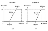
図5を参照して、第1の傷レベル生成回路401乃至第4の傷レベル生成回路404における傷レベルの生成について具体的に説明する。なお、ここでいう傷レベルとは、注目画素の信号が欠陥画素の信号である可能性を示す値である。本実施形態では、傷レベルは、0乃至255の範囲の値で生成され、傷レベルが「0」であれば注目画素の信号が欠陥画素の信号でないことを示している。反対に、傷レベルが「255」であれば注目画素の信号が欠陥画素の信号であることを示している。傷レベルが「0」に近いほど注目画素の信号が欠陥画素の信号でない可能性が高く、傷レベルが「255」に近いほど注目画素の信号が欠陥画素の信号である可能性が高いことを示している。
With reference to FIG. 5, the generation of the flaw level in the first flaw
図5は、第1の傷レベル生成回路401乃至第4の傷レベル生成回路404に入力されるHPF処理の結果の絶対値と第1の傷レベル生成回路401乃至第4の傷レベル生成回路404で生成される傷レベル(の値)との関係を示す図である。図5において、横軸はHPF処理の結果の絶対値HA(HA1乃至HA4)を示し、縦軸は傷レベルDL(DL1乃至DL4)を示している。
FIG. 5 shows the absolute value of the result of HPF processing input to the first flaw
第1の傷レベル生成回路401乃至第4の傷レベル生成回路404は、図5に示す閾値TH2と、傾きの値であるSL1を予め保持している。第1の傷レベル生成回路401乃至第4の傷レベル生成回路404は、以下の式2乃至式4に従って、HPF処理の結果の絶対値HAを傷レベルDL(8ビット)に変換する。
HA≦TH2の場合
DL=0 ・・・(式2)
TH2<HA<TH1の場合
DL=SL1×(HA−TH2) ・・・(式3)
TH1≦HAの場合
DL=1 ・・・(式4)
但し、TH1=TH2+(255/SL1)
例えば、図5に示す例では、入力されるHPF処理の結果の絶対値HAが閾値TH1以上であれば、第1の傷レベル生成回路401乃至第4の傷レベル生成回路404は、傷レベルDL「255」を生成する。一方、入力されるHPF処理の結果の絶対値HAが閾値TH2以下であれば、第1の傷レベル生成回路401乃至第4の傷レベル生成回路404は、傷レベルDL「0」を生成する。また、入力されるHPF処理の結果の絶対値HAが閾値TH2より大きく、閾値TH1より小さければ、第1の傷レベル生成回路401乃至第4の傷レベル生成回路404は、入力されるHPF処理の結果の絶対値が大きいほど大きな値の傷レベルDLを生成する。
The first flaw
When HA ≦ TH2 DL = 0 (Formula 2)
When TH2 <HA <TH1, DL = SL1 × (HA−TH2) (Formula 3)
When TH1 ≦ HA DL = 1 (Formula 4)
However, TH1 = TH2 + (255 / SL1)
For example, in the example shown in FIG. 5, if the absolute value HA of the input HPF process result is equal to or greater than the threshold value TH1, the first flaw
なお、第1の傷レベル生成回路401乃至第4の傷レベル生成回路404は、傷判定回路215から入力される白黒フラグに応じて、欠陥画素が白傷である場合と黒傷である場合とで、閾値TH1及び傾きSL1の値を変更する。例えば、第1の傷レベル生成回路401乃至第4の傷レベル生成回路404は、欠陥画素が白傷である場合には図5(a)に示す特性となるように、欠陥画素が黒傷である場合には図5(b)に示す特性となるように、閾値TH2及び傾きSL1の値を設定する。
Note that the first flaw
また、閾値TH2は、撮像装置100の動作モードなどによって決定される任意の設定値と、輝度信号生成回路214で生成される注目画素の周囲の画素における輝度信号の平均値とを乗算した値とする。輝度が高いとノイズが大きくなるため、輝度信号生成回路214で生成される輝度信号に応じて(即ち、ノイズ量に応じて)閾値TH2を変更することが必要となる。輝度が高いほど閾値TH2を大きくすることによって、ノイズを欠陥画素であると誤判定することを抑制することができる。また、傾きSL1についても、撮像装置100の動作モードなどによって決定される任意の設定値と、輝度信号生成回路214で生成される輝度信号とを乗算した値とする。閾値TH2及び傾きSL1を決定することによって、閾値TH1も決定される。なお、図5に示す絶対値HAに対する傷レベルDLを、式2乃至式4を用いて変換するのではなく、予めテーブルで持つようにしてもよい。
Further, the threshold value TH2 is a value obtained by multiplying an arbitrary setting value determined by the operation mode of the
更に、閾値TH1及び閾値TH2を設定せず、絶対値HAの全範囲において、絶対値HAが増加するほど傷レベルDLが増加するように、絶対値HAに対する傷レベルDLの関係を関数(例えば、3次関数)で定義するようにしてもよい。そして、注目画素の周囲における輝度が高いほど、絶対値HAに対する傷レベルDLの値が小さくなるように、輝度に応じてこの関数を切り替えるようにしてもよい。 Further, the threshold TH1 and the threshold TH2 are not set, and the relationship between the scratch level DL with respect to the absolute value HA is a function (for example, for example, so that the scratch level DL increases as the absolute value HA increases in the entire range of the absolute value HA. It may be defined by a cubic function). Then, this function may be switched according to the luminance so that the higher the luminance around the pixel of interest is, the smaller the value of the scratch level DL with respect to the absolute value HA is.
乗算器405は、第1の傷レベル生成回路401によって生成された傷レベルと第2の傷レベル生成回路402によって生成された傷レベルとを乗算して16ビットの値を求め、これを8ビットにシフト演算してDL5として出力する。乗算器406は、第3の傷レベル生成回路403によって生成された傷レベルと第4の傷レベル生成回路404によって生成された傷レベルとを乗算して16ビットの値を求め、これを8ビットにシフト演算してDL6として出力する。乗算器407は、乗算器405によって乗算された傷レベルDL5と乗算器406によって乗算された傷レベルDL6とを乗算して16ビットの値を求め、これを8ビットにシフト演算して、第1の判定値D1として出力する。
The
このように、閾値判定回路216は、フィルタ処理の結果に基づいて注目画素の信号レベルと、注目画素に周囲に位置する複数の画素の信号レベルとの差分を求める。そして、閾値判定回路216は、その差分が大きいほど注目画素の信号が欠陥画素の信号である可能性が高くなることを示す第1の判定値D1を生成する。
As described above, the
図2に戻って、相関判定回路217は、第1のABS回路210乃至第4のABS回路213のそれぞれから入力されるHPF処理の結果の絶対値HA1乃至HA4の大きさを比較する。相関判定回路217は、この比較結果に基づいて、注目画素の信号が欠陥画素の信号である可能性を示す第2の判定値D2を出力する。
Returning to FIG. 2, the
図6は、相関判定回路217の構成を示す概略ブロック図である。相関判定回路217は、第1の選択回路601と、第2の選択回路602と、第3の選択回路603と、第4の選択回路604と、第5の選択回路605と、第6の選択回路606と、減算器607と、傷レベル判定回路608とを含む。
FIG. 6 is a schematic block diagram showing the configuration of the
第1の選択回路601は、第1のABS回路210から入力されるHPF処理の結果の絶対値HA1と第2のABS回路211から入力されるHPF処理の結果の絶対値HA2とを比較し、大きい方の絶対値を出力する。また、第2の選択回路602は、第1のABS回路210から入力されるHPF処理の結果の絶対値HA1と第2のABS回路211から入力されるHPF処理の結果の絶対値HA2とを比較し、小さい方の絶対値を出力する。
The
第3の選択回路603は、第3のABS回路212から入力されるHPF処理の結果の絶対値HA3と第4のABS回路413から入力されるHPF処理の結果の絶対値HA4とを比較し、大きい方の絶対値を出力する。また、第4の選択回路604は、第3のABS回路212から入力されるHPF処理の結果の絶対値HA3と第4のABS回路413から入力されるHPF処理の結果の絶対値HA4とを比較し、小さい方の絶対値を出力する。
The
第5の選択回路605は、第1の選択回路601から出力された絶対値と第3の選択回路603から出力された絶対値とを比較し、大きい方の絶対値を出力する。第5の選択回路605から出力される絶対値は、第1のABS回路210乃至第4のABS回路213によるHPF処理の結果(即ち、4つの方向のフィルタ処理の結果)のうち最大の絶対値である。
The
第6の選択回路606は、第2の選択回路602から出力された絶対値と第4の選択回路604から出力された絶対値とを比較し、小さい方の絶対値を出力する。第6の選択回路606から出力される絶対値は、第1のABS回路210乃至第4のABS回路213によるHPF処理の結果(即ち、4つの方向のフィルタ処理の結果)のうち最小の絶対値である。
The
減算器607は、第5の選択回路605から出力される絶対値から、第6の選択回路606から出力される絶対値を減算する。減算器607による減算の結果は、第1のABS回路210乃至第4のABS回路213によるHPF処理の結果の最大の差分(差分のばらつき)を示し、最大の絶対値から最小の絶対値を減算したものであるため、必ず0以上の正の値となる。
The
傷レベル判定回路608は、減算器607から出力される絶対値に基づいて第2の判定値D2を生成(算出)して出力する。図7を参照して、傷レベル判定回路608における第2の判定値D2の生成について具体的に説明する。なお、傷レベル判定回路608で生成される第2の判定値D2は、第1の判定値D1と同様に、注目画素の信号が欠陥画素の信号である可能性を示す。図7は、傷レベル判定回路608に入力される減算器607による減算の結果(絶対値HB)と傷レベル判定回路608で生成される第2の判定値D2との関係を示す図である。図7において、横軸は減算器607による減算の結果(絶対値HB)を示し、縦軸は第2の判定値D2を示している。
The flaw
傷レベル判定回路608は、図7に示す閾値TH3と傾きの値であるSL2を予め保持し、以下の式5乃至式7に従って、減算器607による減算の結果を第2の判定値D2(8ビット)に変換する。
HB≦TH3の場合
D2=1 ・・・(式5)
TH3<HB<TH4の場合
D2=SL2×(HB−TH3)+255 ・・・(式6)
TH4≦HBの場合
D2=0 ・・・(式7)
但し、TH4=TH3−(255/SL2)
例えば、図7に示す例では、減算器607による減算の結果HBが閾値TH3以下であれば、傷レベル判定回路608は、第2の判定値D2「255」を生成する。一方、減算器607による減算の結果HBが閾値TH4以上であれば、傷レベル判定回路608は、第2の判定値D2「0」を生成する。また、減算器607による減算の結果HBが閾値TH3より大きく、閾値TH4より小さければ、傷レベル判定回路608は、減算器607による減算の結果(絶対値)が小さいほど大きな値の第2の判定値D2を生成する。
The scratch
When HB ≦ TH3 D2 = 1 (Expression 5)
When TH3 <HB <TH4 D2 = SL2 × (HB−TH3) +255 (Expression 6)
When TH4 ≦ HB D2 = 0 (Expression 7)
However, TH4 = TH3- (255 / SL2)
For example, in the example shown in FIG. 7, if the result HB of the subtraction by the
なお、閾値TH3は、撮像装置100の動作モードなどによって決定される任意の設定値と、輝度信号生成回路214で生成される輝度信号とを乗算した値とする。また、傾きSL2についても、撮像装置100の動作モードなどによって決定される任意の設定値と、輝度信号生成回路214で生成される輝度信号とを乗算した値とする。閾値TH3及び傾きSL2を決定することによって、閾値TH4も決定される。なお、図7に示す減算器607による減算の結果HBに対する第2の判定値D2を、式5乃至式7を用いて変換するのではなく、予めテーブルで持つようにしてもよい。
The threshold value TH3 is a value obtained by multiplying an arbitrary setting value determined by the operation mode of the
このように、相関判定回路217は、フィルタ処理の結果に基づいて注目画素の信号レベルと注目画素に隣接する画素の信号レベルとの差分のばらつき(減算の結果HB)を求める。そして、相関判定回路217は、かかる差分のばらつきが小さいほど、注目画素の信号が欠陥画素の信号である可能性が高くなることを示す第2の判定値D2を生成する。
As described above, the
なお、閾値判定回路216は、画像データに含まれるノイズが大きい場合、かかるノイズによって注目画素の信号を欠陥画素の信号であると誤判定する(即ち、第1の判定値「255」を出力する)可能性がある。そこで、相関判定回路217において、注目画素を含む領域の画像データに含まれるノイズが大きく、差分のばらつきが大きい場合に、注目画素の信号が欠陥画素の信号ではないと判定することが必要となる。
When the noise included in the image data is large, the
また、注目画素が欠陥画素でない場合、第1のABS回路210乃至第4のABS回路213によるHPF処理の結果(即ち、4つの方向のフィルタ処理の結果)は0に近い値となるため、差分のばらつきも0に近い値となる。このような場合、相関判定回路217は、差分のばらつきが小さいために、注目画素の信号を欠陥画素の信号であると誤判定する(即ち、第2の判定値「255」を出力する)可能性がある。そこで、閾値判定回路216において、注目画素の信号レベルと注目画素に隣接する画素の信号レベルとの差分が閾値以上である場合に、注目画素の信号が欠陥画素の信号であると判定することが必要となる。
If the target pixel is not a defective pixel, the results of HPF processing by the
そこで、本実施形態では、図2に示すように、乗算器218において、閾値判定回路216から出力される第1の判定値D1と相関判定回路217から出力される第2の判定値D2とを乗算し、第3の判定値を求める。具体的には、乗算器218は第1の判定値D1と第2の判定値D2を乗算して16ビットの値を求め、これをシフト演算して8ビットの値(即ち、0乃至255の範囲の値)としたものを第3の判定値Kとする。これにより、閾値判定回路216又は相関判定回路217において誤判定があったとしても、相関判定回路217又は閾値判定回路216における判定によって、注目画素が欠陥画素であるかどうかを正しく判定することが可能となる。換言すれば、閾値判定回路216においても、相関判定回路217においても、注目画素が欠陥画素であると判定された場合に、かかる注目画素を欠陥画素として検出する。あるいは、閾値判定回路216においても、相関判定回路217においても、注目画素が欠陥画素である可能性が高いと判定された場合に、注目画素の信号が欠陥画素の信号である可能性が高いものとして検出する。
Therefore, in the present embodiment, as shown in FIG. 2, in the
セレクタ219は、傷判定回路215から入力される傷フラグが「1」であれば(注目画素が欠陥画素であることを示していれば)、乗算器218によって乗算された第3の判定値Kを出力する。また、セレクタ219は、傷判定回路215から入力される傷フラグが「0」であれば(注目画素が欠陥画素でないことを示していれば)、第3の判定値として、「0」を出力する。なお、セレクタ219から出力される傷レベルは、欠陥画素補正回路106に入力される。
If the scratch flag input from the
図8は、欠陥画素補正回路106の構成を示す概略ブロック図である。欠陥画素補正回路106には、A/D変換回路104を介して、欠陥画素を含む画像データが入力される。欠陥画素補正回路106は、補正値算出回路801と、加重加算回路802とを含む。
FIG. 8 is a schematic block diagram showing the configuration of the defective
補正値算出回路801は、例えば、注目画素を参照しないような係数((1、0、1)など)を有するフィルタ処理を行って、欠陥画素の信号レベルを補正するための補正値を算出する。また、補正値算出回路801は、画像データからエッジの方向判別を行い、注目画素におけるエッジの方向に沿った位置に配置された画素の信号レベルを参照して補正値を算出してもよいし、前置補間により補正値を求めてもよい。あるいは、エッジの方向に沿った画素の信号レベルから算出した補正値の重み付けを、それ以外の方向に沿った画素の信号レベルから算出した補正値の重み付けよりも大きくして、これらを加算平均することで補正値としてもよい。
For example, the correction
加重加算回路802は、欠陥画素検出回路105から出力された第3の判定値K(の値)に応じて、A/D変換回路104から出力される注目画素の信号レベルORGと、補正値算出回路801によって算出された補正値CORとを加重加算する。例えば、加重加算回路802は、以下の式8に従って、注目画素の補正後の信号レベルOUTを出力する。
OUT=COR×K+ORG×(255−K) ・・・(式8)
上述したように、第3の判定値Kは、0乃至255の範囲の値である。注目画素が欠陥画素でない(正常な画素である)可能性が高い場合には「0」に近いため、加重加算回路802は、注目画素の信号レベルORGの重みを大きくして補正値CORと加重加算した信号レベル(即ち、欠陥画素が補正された画像データ)OUTを出力する。一方、注目画素が欠陥画素である可能性が高い場合には、第3の判定値Kが「255」に近いため、加重加算回路802は、補正値CORの重みを大きくして注目画素の信号レベルORGと加重加算した信号レベルOUTを出力する。あるいは、第3の判定値Kを所定の閾値と比較し、第3の判定値Kがこの閾値よりも小さければ注目画素の信号レベルORGを、そうでなければ式8に従って求めた値を、補正後の信号レベルOUTとして出力してもよい。
The
OUT = COR × K + ORG × (255−K) (Expression 8)
As described above, the third determination value K is a value in the range of 0 to 255. When there is a high possibility that the target pixel is not a defective pixel (normal pixel), the
以上のように、本実施形態によれば、閾値判定回路216においても、相関判定回路217においても注目画素の信号が欠陥画素の信号であると判定された場合に、注目画素を欠陥画素として検出している。あるいは、閾値判定回路216においても、相関判定回路217においても注目画素の信号が欠陥画素の信号である可能性が高いと判定された場合に、注目画素の信号レベルを欠陥画素の信号レベルである可能性が高いものとして検出している。そのため、従来技術よりも高精度に欠陥画素を検出することができる。更に、閾値判定回路216から出力される傷レベル及び相関判定回路217から出力される傷レベルを乗算した値に応じて注目画素の信号レベルを補正しているため、従来技術よりも高精度に欠陥画素を補正することが可能である。
As described above, according to the present embodiment, when both the
なお、欠陥画素検出回路105は、図9に示すように、第1のLPF回路202及び第2のLPF回路203のそれぞれに対して、互いに異なるハイパスフィルタ処理を行う2つのハイパスフィルタ回路を設けてもよい。
As shown in FIG. 9, the defective
図9を参照するに、第5のHPF回路901及び第6のHPF回路902は、第1のLPF回路202によるLPF処理の結果に対して、水平方向について互いに異なるハイパスフィルタ処理を行う。例えば、第5のHPF回路901は、図10(a)に示すように、低帯域のフィルタ係数((1、2、1)×(1、2、1)×(−1、2、−1))を有するハイパスフィルタ処理(第1のハイパスフィルタを有する第1の高域通過フィルタ処理)を行う。第6のHPF回路902は、図10(b)に示すように、高帯域のフィルタ係数((1、2、1)×(−1、2、−1)×(−1、2、−1))を有するハイパスフィルタ処理(第2のハイパスフィルタを有する第2の高域通過フィルタ処理)を行う。
Referring to FIG. 9, the
第7のHPF回路903及び第8のHPF回路904は、第2のLPF回路203によるLPF処理の結果に対して、垂直方向について互いに異なるハイパスフィルタ処理を行う。例えば、第7のHPF回路903は、低帯域のフィルタ係数を有するハイパスフィルタ処理(図10(a)参照)を行う。第8のHPF回路904は、高帯域のフィルタ係数を有するハイパスフィルタ処理(図10(b)参照)を行う。
The
第5のABS回路905は、第5のHPF回路901によるHPF処理の結果(出力データ)の絶対値を出力する。同様に、第6のABS回路906、第7のABS回路907及び第8のABS回路908のそれぞれは、第6のHPF回路902、第7のHPF回路903及び第8のHPF回路904によるHPF処理の結果(出力データ)の絶対値を出力する。
The
第1の演算回路909及び第2の演算回路910のそれぞれは、同じ構成を有し、閾値判定回路216と、相関判定回路217と、乗算器218とを含む。第1の演算回路909には、第5のABS回路905、第7のABS回路907、第3のABS回路212及び第4のABS回路213のそれぞれからHPF処理の結果の絶対値が入力される。第2の演算回路910には、第6のABS回路906、第8のABS回路908、第3のABS回路212及び第4のABS回路213のそれぞれからHPF処理の結果の絶対値が入力される。
Each of the first
第1の演算回路909及び第2の演算回路910のそれぞれにおいては、同じ帯域のHPF処理の結果の絶対値を用いて、注目画素の信号が欠陥画素の信号である可能性を示す判定値を求める。なお、水平方向、垂直方向、45度方向及び135度方向の全てにおいて、同じ帯域にすることが理想的である。本実施形態において、水平方向及び垂直方向(水平垂直方向)と、45度方向及び135度方向(斜め方向)とでフィルタ係数が異なっているのは、注目画素から参照画素までの距離が水平垂直方向と斜め方向とで異なり、周波数帯域が異なっているからである。
In each of the first
最大値選択回路911は、第1の演算回路909から出力された判定値と第2の演算回路910から出力された判定値とを比較し、大きい方の判定値を出力する。
The maximum
画像データに対して、高域側の周波数帯域でフィルタ処理を行う(図10(b)参照)と、エッジが残る場合があるため、注目画素の信号を欠陥画素の信号と誤判定してしまうことがある。そこで、低域側の周波数帯域でもフィルタ処理を行い、低域に存在する欠陥画素については確実に検出する。そして、エッジに存在するような欠陥画素については、高域側のフィルタ処理の結果と低域側のフィルタ処理の結果とを比較することで、エッジを欠陥画素と誤判定することを抑制することができる。 If the image data is filtered in the high frequency band (see FIG. 10B), an edge may remain, so that the signal of the pixel of interest is erroneously determined to be a defective pixel signal. Sometimes. Therefore, filtering is performed even in the frequency band on the low frequency side, and defective pixels existing in the low frequency are reliably detected. For defective pixels that exist at the edge, the result of filtering on the high-frequency side and the result of filtering on the low-frequency side are compared to suppress erroneous determination of the edge as a defective pixel. Can do.
本実施形態では、G画素に欠陥画素が発生した場合を例に説明したが、R画素及びB画素に欠陥画素が発生した場合についても、R画素以外の画素やB画素以外の画素にゼロ値を挿入して同様な処理を行うことで欠陥画素を検出することが可能である。 In the present embodiment, the case where a defective pixel occurs in the G pixel has been described as an example. However, in the case where a defective pixel occurs in the R pixel and the B pixel, a zero value is set for pixels other than the R pixel and pixels other than the B pixel. It is possible to detect a defective pixel by inserting and inserting the same process.
また、閾値判定回路216及び相関判定回路217は、G画素、R画素及びB画素を区別して第1及び第2の判定値を求める代わりに、式1を用いて求めた輝度信号Yを用いて、第1及び第2の判定値を求めるようにしてもよい。
In addition, the
また、閾値判定回路216が第1の判定値D1を求めるために用いる絶対値HAは、注目画素の周囲に位置する複数の画素の信号レベルに対する、注目画素の信号レベルの差分の大きさを示す値であれば、他の方法で求めた値であってもよい。例えば、閾値判定回路216は、第1のABS回路210乃至第4のABS回路213によるHPF処理の結果の絶対値の平均値を求め、この平均値を絶対値HAとし、絶対値HAを用いて式2乃至式4により第1の判定値D1を求めてもよい。
In addition, the absolute value HA used by the
また、相関判定回路217は、第1のABS回路210乃至第4のABS回路213によるHPF処理の結果の絶対値の分散を求め、この分散の値が小さいほど第2の判定値D2の値を大きく設定するようにしてもよい。
Further, the
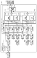
なお、欠陥画素検出回路105は、図2では、LPF回路及びHPF回路で構成されているが、図11に示すように、LPF回路を含まずに構成することも可能である。図11に示す欠陥画素検出回路105の構成について、図2に示す欠陥画素検出回路105の構成と異なる点を中心に、以下に説明する。
In FIG. 2, the defective
第1のHPF回路1101は、G画素以外の画素の信号レベルにゼロ値が挿入された画像データに対して、水平方向について(−1、0、2、0、−1)などのフィルタ係数を有するHPF処理を行う。第1のHPF回路1101は、R画素以外の画素の信号レベルにゼロ値が挿入された画像データ、及び、B画素以外の画素の信号レベルにゼロ値が挿入された画像データに対しても同様にHPF処理を行う。
The
第2のHPF回路1102は、G画素以外の画素の信号レベルにゼロ値が挿入された画像データに対して、垂直方向について(−1、0、2、0、−1)などのフィルタ係数を有するHPF処理を行う。第2のHPF回路1102は、R画素以外の画素の信号レベルにゼロ値が挿入された画像データ、及び、B画素以外の画素の信号レベルにゼロ値が挿入された画像データに対しても同様にHPF処理を行う。
The
第3のHPF回路1103は、G画素以外の画素の信号レベルにゼロ値が挿入された画像データに対して、45度方向について(−1、2、−1)などのフィルタ係数を有するHPF処理を行う。
The
第4のHPF回路1104は、G画素以外の画素の信号レベルにゼロ値が挿入された画像データに対して、135度方向について(−1、2、−1)などのフィルタ係数を有するHPF処理を行う。
The
図11に示す欠陥画素検出回路105の構成では、ゼロ挿入回路201でゼロ値が挿入された画素に対する補間処理が行われないため、各HPF回路は、HPF処理の際にゼロ値が挿入された画素の影響を受けないためのフィルタ係数を有している。水平方向及び垂直方向においては、G画素、R画素及びB画素はいずれも1画素おきに配置されていることから、G画素、R画素及び及びB画素間で、同じフィルタ係数を用いることができる。一方、45度方向及び135度方向においては、R画素及びB画素は1画素おきに配置されているのに対して、G画素は連続して配置されているため、G画素のみをHPF処理の対象としている。
In the configuration of the defective
第1のABS回路1105乃至第4のABS回路1108は、第1のHPF回路1101乃至第4のHPF回路1104によるHPF処理の結果(出力データ)の絶対値を出力する。
The
傷判定回路1109は、図2に示す傷判定回路215と同様に、第1のHPF回路1101乃至第4のHPF回路1104によるHPF処理の結果の符号(正又は負)に応じて、傷フラグと白黒フラグとを出力する。傷判定回路1109は、注目画素がG画素であれば、第1のHPF回路1101、第2のHPF回路1102、第3のHPF回路1103及び第4のHPF回路1104のHPF処理の結果の符号を参照する。また、傷判定回路1109は、注目画素がR画素又はB画素であれば、第1のHPF回路1101及び第2のHPF回路1102のHPF処理の結果の符号を参照する。
Similar to the
閾値判定回路1110は、図2に示す閾値判定回路216と同様に、第1のABS回路1105乃至第4のABS回路1108のそれぞれから入力されるHPF処理の結果の絶対値と、任意に設定された閾値とを比較する。閾値判定回路1110は、この比較結果に基づいて、注目画素の信号が欠陥画素の信号である可能性を示す第1の判定値D1を求める。また、相関判定回路1111は、図2に示す相関判定回路217と同様に、第1のABS回路1105乃至第4のABS回路1108のそれぞれから入力されるHPF処理の結果の絶対値の大きさを比較する。相関判定回路1111は、この比較結果に基づいて、注目画素の信号が欠陥画素の信号である可能性を示す第2の判定値D2を求める。
Similar to the
閾値判定回路1110及び相関判定回路1111は、注目画素がG画素であれば、第1のABS回路1105、第2のABS回路1106、第3のABS回路1107及び第4のABS回路1108のHPF処理の結果の絶対値を参照する。また、閾値判定回路1110及び相関判定回路1111は、注目画素がR画素又はB画素であれば、第1のABS回路1105及び第2のABS回路1106のHPF処理の結果の絶対値を参照する。
If the target pixel is a G pixel, the
そして、図2と同様に、乗算器218が第1の判定値及び第2の判定値を乗算することで得られる第3の判定値が、セレクタ219を介して、欠陥画素補正回路106に入力される。
As in FIG. 2, the third determination value obtained by the
更に、欠陥画素検出回路105は、図2に示すLPF回路やHPF回路などのフィルタ回路に代えて、図12に示すように、差分回路で構成することも可能である。図12に示す欠陥画素検出回路105の構成について、図2に示す欠陥画素検出回路105の構成と異なる点を中心に、以下に説明する。
Further, the defective
第1の差分回路1201は、注目画素の値から、注目画素の右方向に位置する、注目画素から2つ目の注目画素と同色の画素の値を減算した値を求める差分処理を行う。第2の差分回路1202は、注目画素の値から、注目画素の左方向に位置する、注目画素から2つ目の注目画素と同色の画素の値を減算した値を求める差分処理を行う。
The
第3の差分回路1203は、注目画素の値から、注目画素の上方向に位置する、注目画素から2つ目の注目画素と同色の画素の値を減算した値を求める差分処理を行う。第4の差分回路1204は、注目画素の値から、注目画素の下方向に位置する、注目画素から2つ目の注目画素と同色の画素の値を減算した値を求める差分処理を行う。
The
第5の差分回路1205は、注目画素の値から、注目画素の右上方向に位置する、注目画素に隣接する同色の画素の値を減算した値を求める差分処理を行う。第6の差分回路1206は、注目画素の値から、注目画素の左下方向に位置する、注目画素に隣接する同色の画素の値を減算した値を求める差分処理を行う。
The
第7の差分回路1207は、注目画素の値から、注目画素の左上方向に位置する、注目画素に隣接する同色の画素の値を減算した値を求める差分処理を行う。第8の差分回路1208は、注目画素の値から、注目画素の右下方向に位置する、注目画素に隣接する同色の画素の値を減算した値を求める差分処理を行う。
The
このように、第1の差分回路1201乃至第8の差分回路1208は、注目画素の値と、注目画素の周囲に位置する画素の値との差分を求める。第1の差分回路1201乃至第4の差分回路1204は、注目画素がG画素、R画素及びB画素のいずれであっても差分処理を行うが、第5の差分回路1205乃至第8の差分回路1208は、注目画素がG画素である場合のみ差分処理を行うものとする。
In this way, the
第1のABS回路1209乃至第8のABS回路1216は、第1の差分回路1201乃至第8の差分回路1208による差分処理の結果(出力データ)の絶対値を出力する。
The
傷判定回路1217は、図2に示す傷判定回路215と同様に、第1の差分回路1201乃至第8の差分回路1208による差分処理の結果の符号(正又は負)に応じて、傷フラグと白黒フラグとを出力する。傷判定回路1217は、注目画素がG画素であれば、第1の差分回路1201乃至第8の差分回路1208の差分処理の結果の符号を参照する。また、傷判定回路1217は、注目画素がR画素又はB画素であれば、第1の差分回路1201乃至第4の差分回路1204の差分処理の結果の符号を参照する。
Similar to the
閾値判定回路1218は、図2に示す閾値判定回路216と同様に、第1のABS回路1209乃至第8のABS回路1216のそれぞれから入力される差分処理の結果の絶対値と、任意に設定された閾値とを比較する。閾値判定回路1218は、この比較結果に基づいて、注目画素の信号が欠陥画素の信号である可能性を示す第1の判定値を求める。また、相関判定回路1219は、図2に示す相関判定回路217と同様に、第1のABS回路1209乃至第8のABS回路1216のそれぞれから入力される差分処理の結果の絶対値の大きさを比較する。相関判定回路1219は、この比較結果に基づいて、注目画素の信号が欠陥画素の信号である可能性を示す第2の判定値を求める。
Similar to the
なお、閾値判定回路1218及び相関判定回路1219は、注目画素がG画素であれば、第1のABS回路1209乃至第8のABS回路1216の差分処理の結果の絶対値を参照する。また、閾値判定回路1218及び相関判定回路1219は、注目画素がR画素又はB画素であれば、第1のABS回路1209乃至第4のABS回路1212の差分処理の結果の絶対値を参照する。
Note that the
そして、図2と同様に、乗算器218が第1の判定値及び第2の判定値を乗算することで得られる第3の判定値が、セレクタ219を介して、欠陥画素補正回路106に入力される。
As in FIG. 2, the third determination value obtained by the
以上説明したように、本実施形態の欠陥画素検出回路105は、周囲の複数の画素の信号レベルに対する注目画素の信号レベルの差分の大きさを示す第1の判定値を求める。かかる第1の判定値は、周囲の複数の画素の信号レベルに対する注目画素の信号レベルの差分が大きくなるほど、大きな値となる。また、欠陥画素検出回路105は、周囲の複数の画素の信号レベルに対する注目画素の信号レベルの差分の大きさのばらつきを示す第2の判定値を求める。かかる第2の判定値は、周囲の複数の画素の信号レベルに対する注目画素の信号レベルの差分の大きさのばらつきが小さくなるほど、大きな値となる。欠陥画素検出回路105は、第1の判定値D1と第2の判定値D2を乗算し、この乗算によって得られた値が大きいほど、注目画素の信号が欠陥画素の信号である可能性が高いと判定している。なお、欠陥画素検出回路105は、この乗算によって得られた値が閾値以上であった場合に、注目画素の信号が欠陥画素の信号であると判定してもよい。あるいは、欠陥画素検出回路105は、第1の判定値D1と第2の判定値D2のいずれも閾値以上であった場合に、注目画素の信号が欠陥画素の信号であると判定してもよい。
As described above, the defective
更に、欠陥画素補正回路106が、この乗算によって得られた値に基づいて、注目画素に施す補正の程度や補正の可否の判定を行うことにより、従来技術よりも高い精度で欠陥画素の影響を低減させることが可能となる。
Further, the defective
なお、欠陥画素は必ずしも独立して存在するのではなく、欠陥画素が2つ並ぶ可能性もある。これを考慮して、欠陥画素検出回路105は、注目画素の周囲に、注目画素に近い信号レベルを有し、且つ、周囲の他の画素に比較して信号レベルが極端に異なる画素が存在した場合には、この画素の信号レベルを除外して欠陥画素の判定を行うようにしてもよい。
Note that defective pixels do not necessarily exist independently, and two defective pixels may be arranged. In consideration of this, the defective
また、上述した実施形態では、デジタルカメラやビデオカメラなどの撮像装置における欠陥画素の検出処理を例として説明したが、これらに限定されるものではない。例えば、画像処理機能を有するアプリケーションを搭載したパーソナルコンピュータが、着脱可能な記憶媒体やネットワークを介して取得した画像信号に対して、不図示のメモリから読み出したプログラムに従って上述した処理を行うようにしてもよい。 In the above-described embodiments, the detection process of defective pixels in an imaging apparatus such as a digital camera or a video camera has been described as an example. However, the present invention is not limited to this. For example, a personal computer equipped with an application having an image processing function performs the above-described processing according to a program read from a memory (not shown) for an image signal acquired via a removable storage medium or a network. Also good.
また、本発明は、以下の処理を実行することによっても実現される。即ち、上述した実施形態の機能を実現するソフトウェア(プログラム)を、ネットワーク又は各記憶媒体を介してシステム或いは装置に供給し、そのシステム或いは装置のコンピュータ(またはCPUやMPU等)がプログラムを読み出して実行する処理である。この場合、そのプログラム、及び、かかるプログラムを記憶した記憶媒体は本発明を構成することになる。 The present invention can also be realized by executing the following processing. That is, software (program) that realizes the functions of the above-described embodiments is supplied to a system or apparatus via a network or each storage medium, and a computer (or CPU, MPU, etc.) of the system or apparatus reads the program. It is a process to be executed. In this case, the program and the storage medium storing the program constitute the present invention.
以上、本発明の好ましい実施形態について説明したが、本発明はこれらの実施形態に限定されないことはいうまでもなく、その要旨の範囲内で種々の変形及び変更が可能である。例えば、本実施形態では、閾値判定回路で生成される傷レベル及び相関判定回路で生成される傷レベルは8ビットであるが、双方のビット幅が異なっていてもよい。 As mentioned above, although preferable embodiment of this invention was described, it cannot be overemphasized that this invention is not limited to these embodiment, A various deformation | transformation and change are possible within the range of the summary. For example, in the present embodiment, the flaw level generated by the threshold determination circuit and the flaw level generated by the correlation determination circuit are 8 bits, but both bit widths may be different.
Claims (15)
注目画素の周囲に位置する複数の画素の信号レベルに対する、前記注目画素の信号レベルの差分の大きさを示す第1の判定値を求める第1の判定手段と、
前記注目画素の周囲に位置する複数の画素の信号レベルに対する、前記注目画素の信号レベルの差分の大きさのばらつきを示す第2の判定値を求める第2の判定手段と、
前記第1の判定値及び前記第2の判定値を用いて、前記注目画素の信号が欠陥画素の信号であるか否かを検出する検出手段と、を有し、
前記第1の判定手段は、前記注目画素の周囲に位置する複数の画素のそれぞれの信号レベルについて、前記注目画素の信号レベルとの差分を求め、それぞれの差分から前記注目画素の信号が欠陥画素の信号である可能性を示す値を求め、求めた値を乗算することで前記第1の判定値を求めることを特徴とする画像処理装置。 An image processing apparatus that detects a signal of a defective pixel of the image sensor from image data generated by an image sensor composed of a plurality of pixels,
First determination means for obtaining a first determination value indicating a magnitude of a difference in signal level of the target pixel with respect to signal levels of a plurality of pixels located around the target pixel;
Second determination means for obtaining a second determination value indicating a variation in the magnitude of the difference in signal level of the target pixel with respect to the signal levels of a plurality of pixels located around the target pixel;
Detecting means for detecting whether or not the signal of the target pixel is a signal of a defective pixel using the first determination value and the second determination value;
The first determination unit obtains a difference between the signal level of each of a plurality of pixels located around the pixel of interest and the signal level of the pixel of interest, and the signal of the pixel of interest is a defective pixel from each difference. An image processing apparatus characterized in that a first value is obtained by obtaining a value indicating the possibility that the first determination value is obtained, and multiplying the obtained value .
前記検出手段は、前記第1の判定値及び前記第2の判定値のいずれもが、予め定められた閾値以上である場合に、前記注目画素の信号を欠陥画素の信号として検出することを特徴とする請求項1に記載の画像処理装置。The detection unit detects the signal of the target pixel as a signal of a defective pixel when both the first determination value and the second determination value are equal to or greater than a predetermined threshold value. The image processing apparatus according to claim 1.
前記第1の判定手段は、前記高域通過フィルタ処理の結果の絶対値から、前記第1の判定値を求め、
前記第2の判定手段は、前記高域通過フィルタ処理の結果の絶対値のばらつきから、前記第2の判定値を求めることを特徴とする請求項1乃至3のうちいずれか1項に記載の画像処理装置。 In the region including the target pixel, the processing unit further includes a high-pass filter process for a plurality of directions with the target pixel as a center,
The first determination means obtains the first determination value from the absolute value of the result of the high-pass filter processing,
The said 2nd determination means calculates | requires a said 2nd determination value from the dispersion | variation in the absolute value of the result of the said high-pass filter process, The any one of Claims 1 thru | or 3 characterized by the above-mentioned. Image processing device.
前記注目画素を中心としていずれかの方向に前記低域通過フィルタ処理を行ってから、前記注目画素を中心として前記低域通過フィルタ処理とは異なる方向に前記高域通過フィルタ処理を行うことを特徴とする請求項4に記載の画像処理装置。 The processing means performs the high-pass filter processing after performing low-pass filter processing in a plurality of directions around the target pixel in a region including the target pixel,
The low-pass filter processing is performed in any direction around the target pixel, and then the high-pass filter processing is performed in a direction different from the low-pass filter processing around the target pixel. The image processing apparatus according to claim 4.
複数の前記処理手段のそれぞれに対応して設けられた複数の前記第1の判定手段及び複数の前記第2の判定手段と、
いずれか1つの前記処理手段に対応した前記第1の判定手段と前記第2の判定手段によって求められた前記第1の判定値及び前記第2の判定値から得られた値を選択する選択手段と、を更に有することを特徴とする請求項4に記載の画像処理装置。 A plurality of processing means for performing high-pass filter processing with different bands;
A plurality of the first determination means and a plurality of the second determination means provided corresponding to each of the plurality of processing means;
Selection means for selecting a value obtained from the first judgment value and the second judgment value obtained by the first judgment means and the second judgment means corresponding to any one of the processing means. The image processing apparatus according to claim 4, further comprising:
注目画素の周囲に位置する複数の画素の信号レベルに対する、前記注目画素の信号レベルの差分の大きさを示す第1の判定値を求める第1の判定手段と、
前記注目画素の周囲に位置する複数の画素の信号レベルに対する、前記注目画素の信号レベルの差分の大きさのばらつきを示す第2の判定値を求める第2の判定手段と、
前記第1の判定値と前記第2の判定値を乗算して得られた値を用いて、前記注目画素の信号レベルと、前記注目画素の周囲に位置する画素の信号レベルから求めた補正値を重み付け加算することで、前記注目画素の信号レベルを補正する補正手段と、を有し、
前記第1の判定値は前記差分の大きさが大きいほど大きな値となり、前記第2の判定値は前記差分の大きさのばらつきが小さいほど大きな値となるものであって、
前記補正手段は、前記第1の判定値と前記第2の判定値を乗算して得られた値が大きいほど、前記補正値の重み付けを大きくすることを特徴とする画像処理装置。 An image processing apparatus that detects a signal of a defective pixel of the image sensor from image data generated by an image sensor composed of a plurality of pixels,
First determination means for obtaining a first determination value indicating a magnitude of a difference in signal level of the target pixel with respect to signal levels of a plurality of pixels located around the target pixel;
Second determination means for obtaining a second determination value indicating a variation in the magnitude of the difference in signal level of the target pixel with respect to the signal levels of a plurality of pixels located around the target pixel;
Using the value obtained by multiplying the first determination value and the second determination value, a correction value obtained from the signal level of the target pixel and the signal level of pixels located around the target pixel Correction means for correcting the signal level of the pixel of interest by weighted addition,
The first determination value is a larger value as the difference is larger, and the second determination value is a larger value as the variation in the difference is smaller.
The image processing apparatus, wherein the correction unit increases the weight of the correction value as the value obtained by multiplying the first determination value and the second determination value is larger.
前記第1の判定手段は、前記高域通過フィルタ処理の結果の絶対値から、前記第1の判定値を求め、
前記第2の判定手段は、前記高域通過フィルタ処理の結果の絶対値のばらつきから、前記第2の判定値を求めることを特徴とする請求項7に記載の画像処理装置。 In the region including the target pixel, the processing unit further includes a high-pass filter process for a plurality of directions with the target pixel as a center,
The first determination means obtains the first determination value from the absolute value of the result of the high-pass filter processing,
The image processing apparatus according to claim 7, wherein the second determination unit obtains the second determination value from a variation in absolute value as a result of the high-pass filter processing.
前記注目画素を中心としていずれかの方向に前記低域通過フィルタ処理を行ってから、前記注目画素を中心として前記低域通過フィルタ処理とは異なる方向に前記高域通過フィルタ処理を行うことを特徴とする請求項9に記載の画像処理装置。 The processing means performs the high-pass filter processing after performing low-pass filter processing in a plurality of directions around the target pixel in a region including the target pixel,
The low-pass filter processing is performed in any direction around the target pixel, and then the high-pass filter processing is performed in a direction different from the low-pass filter processing around the target pixel. The image processing apparatus according to claim 9.
複数の前記処理手段のそれぞれに対応して設けられた複数の前記第1の判定手段及び複数の前記第2の判定手段と、
いずれか1つの前記処理手段に対応した前記第1の判定手段と前記第2の判定手段によって求められた前記第1の判定値及び前記第2の判定値から得られた値を選択する選択手段と、を更に有することを特徴とする請求項9又は10に記載の画像処理装置。 A plurality of processing means for performing high-pass filter processing with different bands;
A plurality of the first determination means and a plurality of the second determination means provided corresponding to each of the plurality of processing means;
Selection means for selecting a value obtained from the first judgment value and the second judgment value obtained by the first judgment means and the second judgment means corresponding to any one of the processing means. The image processing apparatus according to claim 9, further comprising:
第1の判定手段が、注目画素の周囲に位置する複数の画素の信号レベルに対する、前記注目画素の信号レベルの差分の大きさを示す第1の判定値を求めるステップと、
第2の判定手段が、前記注目画素の周囲に位置する複数の画素の信号レベルに対する、前記注目画素の信号レベルの差分の大きさのばらつきを示す第2の判定値を求めるステップと、
検出手段が、前記第1の判定値及び前記第2の判定値を用いて、前記注目画素の信号が欠陥画素の信号であるか否かを検出するステップと、
を有し、
前記第1の判定値を求めるステップでは、前記注目画素の周囲に位置する複数の画素のそれぞれの信号レベルについて、前記注目画素の信号レベルとの差分を求め、それぞれの差分から前記注目画素の信号が欠陥画素の信号である可能性を示す値を求め、求めた値を乗算することで前記第1の判定値を求めることを特徴とする制御方法。 A control method of an image processing apparatus for detecting a signal of a defective pixel of the image sensor from image data generated by an image sensor composed of a plurality of pixels,
The first determination unit, and determining relative signal level of a plurality of pixels located around the pixel of interest, the first determination value shows the magnitude of the difference of the signal level of the pixel of interest,
The second determination means, determining a second judgment value to indicate to the signal level of a plurality of pixels, the variation in the magnitude of the difference of the signal level of the pixel of interest is located around the pixel of interest,
A step of detecting means, using the first determination value and the second judgment value, the signal of the pixel of interest is detected whether the signal of the defective pixel,
I have a,
In the step of obtaining the first determination value, a difference between the signal level of each of a plurality of pixels located around the pixel of interest and a signal level of the pixel of interest is obtained, and the signal of the pixel of interest is obtained from each difference. A control method characterized in that a value indicating the possibility that is a signal of a defective pixel is obtained, and the first determination value is obtained by multiplying the obtained value .
前記欠陥画素の信号を検出するステップでは、前記第1の判定値及び前記第2の判定値のいずれもが、予め定められた閾値以上である場合に、前記注目画素の信号を欠陥画素の信号として検出することを特徴とする請求項12に記載の制御方法。In the step of detecting the signal of the defective pixel, when both the first determination value and the second determination value are equal to or greater than a predetermined threshold, the signal of the target pixel is determined as the signal of the defective pixel. The control method according to claim 12, wherein the control method is detected as:
第1の判定手段が、注目画素の周囲に位置する複数の画素の信号レベルに対する、前記注目画素の信号レベルの差分の大きさを示すものであって、前記差分の大きさが大きいほど大きな値となる第1の判定値を求めるステップと、
第2の判定手段が、前記注目画素の周囲に位置する複数の画素の信号レベルに対する、前記注目画素の信号レベルの差分の大きさのばらつきを示すものであって、前記差分の大きさのばらつきが小さいほど大きな値となる第2の判定値を求めるステップと、
補正手段が、前記第1の判定値と前記第2の判定値を乗算して得られた値が大きいほど、前記注目画素の周囲に位置する画素の信号レベルから求めた補正値の重み付けを大きくして、前記注目画素の信号レベルと前記補正値を重み付け加算することで、前記注目画素の信号レベルを補正するステップと、
を有することを特徴とする制御方法。 A control method of an image processing apparatus for detecting a signal of a defective pixel of the image sensor from image data generated by an image sensor composed of a plurality of pixels,
The first determination means indicates the magnitude of the difference in signal level of the target pixel with respect to the signal levels of a plurality of pixels located around the target pixel, and the larger the difference, the larger the value. Obtaining a first determination value that becomes:
The second determination means indicates a variation in the difference in the signal level of the pixel of interest with respect to the signal levels of a plurality of pixels located around the pixel of interest, and the variation in the difference in size Obtaining a second determination value that becomes a larger value as the value becomes smaller;
As the value obtained by the correction means multiplying the first determination value and the second determination value is larger, the weight of the correction value obtained from the signal level of the pixel located around the target pixel is increased. And correcting the signal level of the pixel of interest by weighting and adding the signal level of the pixel of interest and the correction value;
A control method characterized by comprising:
Priority Applications (7)
| Application Number | Priority Date | Filing Date | Title |
|---|---|---|---|
| JP2010073472A JP5697353B2 (en) | 2010-03-26 | 2010-03-26 | Image processing apparatus, image processing apparatus control method, and program |
| PCT/JP2011/054217 WO2011118329A1 (en) | 2010-03-26 | 2011-02-18 | Image processing apparatus and control method for image processing apparatus |
| RU2012145612/08A RU2527198C2 (en) | 2010-03-26 | 2011-02-18 | Image processing device and image processing device control method |
| CN201180016308.XA CN102835102B (en) | 2010-03-26 | 2011-02-18 | Image processing apparatus and control method for image processing apparatus |
| GB1219314.0A GB2494064B (en) | 2010-03-26 | 2011-02-18 | Image processing apparatus and control method for image processing apparatus |
| US13/521,372 US8922680B2 (en) | 2010-03-26 | 2011-02-18 | Image processing apparatus and control method for image processing apparatus |
| DE112011101066.4T DE112011101066B4 (en) | 2010-03-26 | 2011-02-18 | IMAGE PROCESSING DEVICE AND CONTROL METHOD FOR AN IMAGE PROCESSING DEVICE |
Applications Claiming Priority (1)
| Application Number | Priority Date | Filing Date | Title |
|---|---|---|---|
| JP2010073472A JP5697353B2 (en) | 2010-03-26 | 2010-03-26 | Image processing apparatus, image processing apparatus control method, and program |
Related Child Applications (1)
| Application Number | Title | Priority Date | Filing Date |
|---|---|---|---|
| JP2015025595A Division JP5957106B2 (en) | 2015-02-12 | 2015-02-12 | Image processing apparatus, image processing apparatus control method, and program |
Publications (3)
| Publication Number | Publication Date |
|---|---|
| JP2011205586A JP2011205586A (en) | 2011-10-13 |
| JP2011205586A5 JP2011205586A5 (en) | 2013-05-09 |
| JP5697353B2 true JP5697353B2 (en) | 2015-04-08 |
Family
ID=44672900
Family Applications (1)
| Application Number | Title | Priority Date | Filing Date |
|---|---|---|---|
| JP2010073472A Active JP5697353B2 (en) | 2010-03-26 | 2010-03-26 | Image processing apparatus, image processing apparatus control method, and program |
Country Status (7)
| Country | Link |
|---|---|
| US (1) | US8922680B2 (en) |
| JP (1) | JP5697353B2 (en) |
| CN (1) | CN102835102B (en) |
| DE (1) | DE112011101066B4 (en) |
| GB (1) | GB2494064B (en) |
| RU (1) | RU2527198C2 (en) |
| WO (1) | WO2011118329A1 (en) |
Families Citing this family (16)
| Publication number | Priority date | Publication date | Assignee | Title |
|---|---|---|---|---|
| JP5774456B2 (en) * | 2011-11-30 | 2015-09-09 | 日立マクセル株式会社 | Imaging device |
| JP5900194B2 (en) * | 2012-07-02 | 2016-04-06 | ソニー株式会社 | Signal processing apparatus, signal processing method, program, solid-state imaging device, and electronic apparatus |
| US9088740B2 (en) * | 2013-06-21 | 2015-07-21 | Himax Imaging Limited | System and method of reducing noise |
| JP5970012B2 (en) | 2014-02-27 | 2016-08-17 | キヤノン株式会社 | Image processing apparatus and control method thereof |
| JP6045523B2 (en) * | 2014-02-27 | 2016-12-14 | キヤノン株式会社 | Image processing apparatus and control method thereof |
| US10021324B2 (en) * | 2014-03-12 | 2018-07-10 | SZ DJI Technology Co., Ltd. | Method and system of correcting defective pixels |
| RU2556885C1 (en) * | 2014-06-17 | 2015-07-20 | Закрытое акционерное общество "Электронно-вычислительные информационные и инструментальные системы" (ЗАО "ЭЛВИИС") | Method and system for correcting defective image pixels |
| EP3660782B1 (en) * | 2015-03-06 | 2022-08-10 | Teledyne Flir, LLC | Anomalous pixel detection |
| US10354577B1 (en) * | 2015-06-02 | 2019-07-16 | X Development Llc | Masking non-functioning pixels in a display |
| JP2017055308A (en) * | 2015-09-10 | 2017-03-16 | キヤノン株式会社 | Imaging apparatus and its control method |
| JP2017055309A (en) | 2015-09-10 | 2017-03-16 | キヤノン株式会社 | Imaging apparatus and its control method |
| WO2017221376A1 (en) * | 2016-06-23 | 2017-12-28 | オリンパス株式会社 | Image processing device, image processing method, and image processing program |
| JP7084801B2 (en) * | 2018-07-03 | 2022-06-15 | キヤノン株式会社 | Image sensor and image sensor |
| US10950199B1 (en) * | 2019-10-11 | 2021-03-16 | Facebook Technologies, Llc | Systems and methods for hiding dead pixels |
| KR20220048090A (en) * | 2020-10-12 | 2022-04-19 | 삼성전자주식회사 | Method of testing image sensor using frequency domain and test system performing the same |
| US20230342897A1 (en) * | 2022-04-26 | 2023-10-26 | Communications Test Design, Inc. | Method to detect camera blemishes |
Family Cites Families (22)
| Publication number | Priority date | Publication date | Assignee | Title |
|---|---|---|---|---|
| US6529622B1 (en) * | 1998-10-30 | 2003-03-04 | General Electric Company | Method and apparatus for identifying defective regions in a discrete pixel detector |
| US6625318B1 (en) * | 1998-11-13 | 2003-09-23 | Yap-Peng Tan | Robust sequential approach in detecting defective pixels within an image sensor |
| FR2786648B1 (en) * | 1998-11-30 | 2001-01-05 | Commissariat Energie Atomique | METHOD FOR CORRECTING IMAGE DEFECTS FROM A MATRIX TYPE X OR Y-RAY DETECTOR |
| JP4006137B2 (en) * | 1999-06-18 | 2007-11-14 | キヤノン株式会社 | Image processing apparatus, image processing system, and image processing method |
| JP2001086517A (en) | 1999-09-13 | 2001-03-30 | Toshiba Corp | Pixel defect detector |
| US7283165B2 (en) * | 2002-11-15 | 2007-10-16 | Lockheed Martin Corporation | Method and apparatus for image processing using weighted defective pixel replacement |
| EP1672912B1 (en) * | 2003-01-16 | 2012-03-14 | DigitalOptics Corporation International | Method for producing an optical system including an electronic image enhancement processor |
| JP2004297267A (en) | 2003-03-26 | 2004-10-21 | Sharp Corp | Pixel defect processor |
| JP4346968B2 (en) * | 2003-06-13 | 2009-10-21 | キヤノン株式会社 | Radiation imaging method, radiation imaging apparatus, and computer program |
| JP4453332B2 (en) * | 2003-10-17 | 2010-04-21 | ソニー株式会社 | Defective pixel detection method, detection apparatus, and imaging apparatus |
| JP2005341244A (en) * | 2004-05-27 | 2005-12-08 | Sony Corp | Imaging device, defective pixel detecting method, and program |
| US7460688B2 (en) | 2004-12-09 | 2008-12-02 | Aptina Imaging Corporation | System and method for detecting and correcting defective pixels in a digital image sensor |
| US7450167B2 (en) * | 2005-02-11 | 2008-11-11 | Hewlett-Packard Development Company, L.P. | Method for improving image quality |
| KR100652408B1 (en) * | 2005-04-27 | 2006-12-01 | 삼성전자주식회사 | Method and apparatus for processing Bayer-pattern color digital image signal |
| RU2378790C1 (en) * | 2005-09-27 | 2010-01-10 | Квэлкомм Инкорпорейтед | Scalability techniques based on content information |
| CN100464590C (en) | 2005-11-16 | 2009-02-25 | 北京中星微电子有限公司 | Defect pixel detecting method |
| JP2008131161A (en) * | 2006-11-17 | 2008-06-05 | Rohm Co Ltd | Defective pixel detecting device, electronic apparatus, and defective pixel detecting program |
| JP4703601B2 (en) * | 2007-04-27 | 2011-06-15 | 株式会社東芝 | Imaging device |
| JP2009145285A (en) | 2007-12-18 | 2009-07-02 | Dainippon Screen Mfg Co Ltd | Defect detecting method and defect detecting apparatus |
| JP5692691B2 (en) | 2008-05-09 | 2015-04-01 | Nltテクノロジー株式会社 | Display device inspection method, inspection device, display device substrate, and display device |
| JP5311945B2 (en) | 2008-09-16 | 2013-10-09 | キヤノン株式会社 | Imaging apparatus and defective pixel detection method |
| JP2010073472A (en) | 2008-09-18 | 2010-04-02 | Sumitomo Electric Ind Ltd | Anisotropic conduction sheet, method of manufacturing the same, mounting module, and electronic product |
-
2010
- 2010-03-26 JP JP2010073472A patent/JP5697353B2/en active Active
-
2011
- 2011-02-18 GB GB1219314.0A patent/GB2494064B/en active Active
- 2011-02-18 WO PCT/JP2011/054217 patent/WO2011118329A1/en active Application Filing
- 2011-02-18 DE DE112011101066.4T patent/DE112011101066B4/en not_active Expired - Fee Related
- 2011-02-18 RU RU2012145612/08A patent/RU2527198C2/en active
- 2011-02-18 US US13/521,372 patent/US8922680B2/en active Active
- 2011-02-18 CN CN201180016308.XA patent/CN102835102B/en active Active
Also Published As
| Publication number | Publication date |
|---|---|
| JP2011205586A (en) | 2011-10-13 |
| WO2011118329A1 (en) | 2011-09-29 |
| GB2494064A (en) | 2013-02-27 |
| RU2527198C2 (en) | 2014-08-27 |
| US20120281123A1 (en) | 2012-11-08 |
| RU2012145612A (en) | 2014-05-10 |
| CN102835102A (en) | 2012-12-19 |
| US8922680B2 (en) | 2014-12-30 |
| DE112011101066T5 (en) | 2013-01-24 |
| GB201219314D0 (en) | 2012-12-12 |
| GB2494064B (en) | 2016-04-13 |
| DE112011101066B4 (en) | 2020-02-06 |
| CN102835102B (en) | 2015-07-01 |
Similar Documents
| Publication | Publication Date | Title |
|---|---|---|
| JP5697353B2 (en) | Image processing apparatus, image processing apparatus control method, and program | |
| JP5631325B2 (en) | Defect detection method for imaging apparatus and imaging apparatus | |
| TWI430654B (en) | Temporal filtering techniques for image signal processing | |
| JP4709084B2 (en) | Image processing apparatus and image processing method | |
| TWI454153B (en) | System and method for demosaicing image data using weighted gradients | |
| TWI425831B (en) | System and method for detecting and correcting defective pixels in an image sensor | |
| US8436910B2 (en) | Image processing apparatus and image processing method | |
| JP4395789B2 (en) | Image processing apparatus, imaging apparatus, image processing method, and program | |
| JP5060535B2 (en) | Image processing device | |
| JP5112238B2 (en) | Imaging apparatus, setting value changing method, and program | |
| JP2013219705A (en) | Image processor, image processing method and program | |
| JP5847471B2 (en) | Image processing apparatus, imaging apparatus, image processing method, and image processing program | |
| JP5169994B2 (en) | Image processing apparatus, imaging apparatus, and image processing method | |
| JP4717371B2 (en) | Image processing apparatus and image processing program | |
| WO2014013792A1 (en) | Noise evaluation method, image processing device, imaging device, and program | |
| JP4945943B2 (en) | Image processing device | |
| JP4945942B2 (en) | Image processing device | |
| JP5957106B2 (en) | Image processing apparatus, image processing apparatus control method, and program | |
| JP5178421B2 (en) | Image processing apparatus, image processing method, and imaging apparatus | |
| JP2011114473A (en) | Pixel defect correction device | |
| JP2011114760A (en) | Method for inspecting camera module | |
| JP5228929B2 (en) | Image processing apparatus, imaging apparatus, and image processing program | |
| JP2013225772A (en) | Image processing device and method | |
| JP2010161563A (en) | Image processing apparatus and image processing method | |
| JP2013055622A (en) | Image processing apparatus, image processing method, information recording medium, and program |
Legal Events
| Date | Code | Title | Description |
|---|---|---|---|
| A521 | Request for written amendment filed |
Free format text: JAPANESE INTERMEDIATE CODE: A523 Effective date: 20130326 |
|
| A621 | Written request for application examination |
Free format text: JAPANESE INTERMEDIATE CODE: A621 Effective date: 20130326 |
|
| A131 | Notification of reasons for refusal |
Free format text: JAPANESE INTERMEDIATE CODE: A131 Effective date: 20140502 |
|
| A521 | Request for written amendment filed |
Free format text: JAPANESE INTERMEDIATE CODE: A523 Effective date: 20140606 |
|
| TRDD | Decision of grant or rejection written | ||
| A01 | Written decision to grant a patent or to grant a registration (utility model) |
Free format text: JAPANESE INTERMEDIATE CODE: A01 Effective date: 20150113 |
|
| A61 | First payment of annual fees (during grant procedure) |
Free format text: JAPANESE INTERMEDIATE CODE: A61 Effective date: 20150210 |
|
| R151 | Written notification of patent or utility model registration |
Ref document number: 5697353 Country of ref document: JP Free format text: JAPANESE INTERMEDIATE CODE: R151 |