Die vorliegende Erfindung bezieht sich auf ein Bildverarbeitungsgerät, das ein Signal von einem defekten Pixel (Bildelement) in einem Bildsensor erfasst, und auf ein Steuerungsverfahren für das Bildverarbeitungsgerät.The present invention relates to an image processing device that detects a signal from a defective pixel (picture element) in an image sensor, and a control method for the image processing device.
STAND DER TECHNIKSTATE OF THE ART
Abbildungsgeräte wie zum Beispiel Digitalkameras oder digitale Videokameras wenden im Allgemeinen CCD-Sensoren oder CMOS-Sensoren als Bildsensoren an, in denen Farbfilter angeordnet sind. Bei derartigen Bildsensoren gibt es Fälle, in denen ein defektes Pixel (auch als ein sogenannter „Flimmerdefekt“ bezeichnet) aufgrund struktureller Faktoren, Faktoren, die während des Herstellungsprozesses auftreten, externen Faktoren, die nach der Herstellung auftreten, usw. auftritt. Zum Beispiel ist ein Beispiel der Faktoren, die defekte Pixel in einem CMOS-Sensor erzeugen, ein Rauschen, das bei einer Floating-Diffusion auftritt, bei der Ladungen von Fotodioden empfangen werden. Ein derartiges Rauschen tritt nicht immer periodisch auf, so dass manchmal ein Rauschen in regelmäßigen Abständen auftreten kann wie zum Beispiel alle paar Mal, wenn ein Aufnahme- bzw. Abbildungsvorgang ausgeführt wird, und manchmal ein Rauschen in unregelmäßigen Abständen auftreten kann wie zum Beispiel alle paar Jahre. Es ist ferner bekannt, dass die Häufigkeit des Auftretens von defekten Pixel in einem Bildsensor nicht von der Temperatur und der Aufladeausbildungszeit abhängt.Imaging devices such as digital cameras or digital video cameras generally use CCD sensors or CMOS sensors as image sensors in which color filters are arranged. With such image sensors, there are cases where a defective pixel (also called a so-called "flicker defect") occurs due to structural factors, factors that occur during the manufacturing process, external factors that occur after manufacturing, etc. For example, an example of the factors that produce defective pixels in a CMOS sensor is noise that occurs in floating diffusion when charges from photodiodes are received. Such noise does not always occur periodically, so sometimes noise may occur at regular intervals, such as every few times when a picture is taken, and sometimes noise may occur at irregular intervals, such as every few times years. It is also known that the frequency of occurrence of defective pixels in an image sensor does not depend on the temperature and the charging formation time.
In dieser Hinsicht wurden Techniken zum Erfassen eines defekten Pixels in einem Bildsensor in JP 2004-297267 A und JP 2001-086517 A vorgeschlagen. Mit diesen Techniken ist es möglich, nicht nur ein defektes Pixel, das in einer bestimmten Position während des Herstellungsprozesses auftritt, sondern auch ein defektes Pixel zu erfassen, das nach einer Herstellung auftritt. Zum Beispiel offenbart JP 2004-297267 A eine Technik für jeden Farbfilter zum Erhalten einer Differenz in einem Signalniveau zwischen einem bestimmen Pixel und einer Vielzahl von benachbarten Pixel des bestimmten Pixels und, wenn alle Differenzen größer sind als oder gleich sind wie ein Grenzwert, wird das bestimmte Pixel als ein defektes Pixel erfasst. JP 2001-086517 A offenbart eine Technik zum Erhalten von Luminanzwerten von allen Pixel unabhängig von der Farbe der Farbfilter und, wenn eine Differenz des Luminanzniveaus zwischen einem bestimmten Pixel und einer Vielzahl von benachbarten Pixel größer ist als oder gleich ist wie ein Grenzwert, wird das bestimmte Pixel als ein defektes Pixel erfasst.In this regard, techniques for detecting a defective pixel in an image sensor have been shown in FIG JP 2004-297267 A and JP 2001-086517 A proposed. With these techniques, it is possible to detect not only a defective pixel that occurs in a certain position during the manufacturing process, but also a defective pixel that occurs after manufacturing. For example revealed JP 2004-297267 A one technique for each color filter to obtain a difference in signal level between a particular pixel and a plurality of adjacent pixels of the particular pixel and if all differences are greater than or equal to a threshold, the particular pixel is detected as a defective pixel. JP 2001-086517 A discloses a technique for obtaining luminance values from all pixels regardless of the color of the color filters, and if a difference in luminance level between a particular pixel and a plurality of adjacent pixels is greater than or equal to a threshold, the particular pixel is considered a defective one Pixels captured.
Jedoch kann mit den konventionellen Techniken ein defektes Pixel, das in einem Bildsensor auftritt, nicht mit hoher Genauigkeit erfasst werden. Zum Beispiel wird mit der Technik, die in JP 2004-297267 A offenbart ist, in dem Fall, in dem ein hochempfindliches Abbilden (Aufnehmen) ausgeführt wird, der Verstärkungsfaktor der Bilddaten (Bildsignal) erhöht und demgemäß wird eine Rauschkomponente, die in den Bilddaten umfasst ist, auch verstärkt, so dass in einigen Fällen die Rauschkomponente markanter sein kann als die Signalniveaus der benachbarten Pixel des bestimmten Pixels. Insbesondere ist es in einer Region, in der die Ortsfrequenz eines Objekts niedrig ist, wahrscheinlicher, dass eine derartige Rauschkomponente einen größeren Wert aufweist als die Signalniveaus der benachbarten Pixel des bestimmten Pixels, und als Ergebnis wird die Differenz des Signalniveaus zwischen dem bestimmten Pixel und den benachbarten Pixel größer als ein Grenzwert und kann das bestimmte Pixel fehlerhaft als ein defektes Pixel erfasst werden. Es ist anzumerken, dass, obwohl es vorstellbar ist, dass der Grenzwert auf einen hohen Wert festgelegt wird, um eine derartige fehlerhafte Erfassung zu vermeiden, es in einer Region schwierig ist, in der das Signalniveau hoch ist, ein defektes Pixel zu erfassen, da die Differenz des Signalniveaus zwischen dem bestimmten Pixel und den benachbarten Pixel gering ist (d.h. weniger ausgeprägt ist). Ähnliche Probleme wie in JP 2004-297267 A treten auch bei der Technik auf, die in JP 2001-086517 A offenbart ist.However, with the conventional techniques, a defective pixel that occurs in an image sensor cannot be detected with high accuracy. For example, with the technique used in JP 2004-297267 A is disclosed, in the case where highly sensitive imaging is performed, the amplification factor of the image data (image signal) is increased, and accordingly, a noise component included in the image data is also amplified, so that in some cases the noise component is more distinctive can be than the signal levels of the neighboring pixels of the particular pixel. In particular, in a region where the spatial frequency of an object is low, such a noise component is more likely to have a larger value than the signal levels of the neighboring pixels of the particular pixel, and as a result, the difference in the signal level between the particular pixel and the neighboring pixels larger than a limit and the particular pixel may be erroneously detected as a defective pixel. It should be noted that, although it is conceivable that the threshold is set high to avoid such erroneous detection, it is difficult to detect a defective pixel in a region where the signal level is high the difference in signal level between the particular pixel and the neighboring pixels is small (ie less pronounced). Similar problems as in JP 2004-297267 A also occur in the technology used in JP 2001-086517 A is disclosed.
US 7 362 916 B2 zeigt ein Bildverarbeitungsgerät und ein Steuerungsverfahren für ein Bildverarbeitungsgerät zum Erfassen eines Signals von einem defekten Pixel eines Bildsensors aus Bilddaten, die durch den Bildsensor erzeugt werden, der durch eine Vielzahl von Pixel gebildet ist, wobei das Gerät/Verfahren Folgendes aufweist: eine erste Bestimmungseinrichtung zum Erhalten eines ersten Bestimmungswerts, der eine Stärke einer Differenz eines Signalniveaus zwischen einem bestimmten Pixel und einer Vielzahl von Pixel bestimmt, die in der Umgebung des bestimmten Pixels angeordnet sind; eine zweite Bestimmungseinrichtung zum Erhalten eines zweiten Bestimmungswerts, der eine Verteilungsbreite der Differenz des Signalniveaus zwischen dem bestimmten Pixel und der Vielzahl von Pixel bestimmt, die in der Umgebung des bestimmten Pixels angeordnet sind; und eine Erfassungseinrichtung zum Erfassen, ob das Signal von dem bestimmten Pixel ein defektes Pixelsignal ist oder nicht, mittels des ersten Bestimmungswerts und des zweiten Bestimmungswerts, wobei der erste Bestimmungswert ein Wert ist, der sich erhöht, wenn sich die Stärke der Differenz erhöht, und der zweite Bestimmungswert ein Wert ist, der sich erhöht, wenn sich die Verteilungsbreite der Stärke der Differenz verringert, und die Erfassungseinrichtung das Signal von dem bestimmten Pixel als ein defektes Pixelsignal erfasst, wenn sowohl der erste Bestimmungswert als auch der zweite Bestimmungswert größer sind als oder gleich sind wie ein vorbestimmter Grenzwert. US 7 362 916 B2 shows an image processing device and a control method for an image processing device for detecting a signal from a defective pixel of an image sensor from image data generated by the image sensor, which is formed by a plurality of pixels, the device / method comprising: a first determination device for Obtaining a first determination value that determines a magnitude of a difference in signal level between a particular pixel and a plurality of pixels located in the vicinity of the particular pixel; second determination means for obtaining a second determination value which determines a distribution width of the difference in signal level between the determined pixel and the plurality of pixels arranged in the vicinity of the determined pixel; and detection means for detecting whether or not the signal from the determined pixel is a defective pixel signal by means of the first determination value and the second determination value, the first determination value being a value that increases as the magnitude of the difference increases, and the second determination value is a value that increases as the distribution width of the magnitude of the difference decreases, and the detector detects the signal from the determined pixel as a defective pixel signal when both the first determination value and the second Determination value is greater than or equal to a predetermined limit.
US 6 296 387 B1 zeigt ein Bildverarbeitungsgerät und ein Steuerungsverfahren für ein Bildverarbeitungsgerät zum Erfassen eines Signals von einem defekten Pixel eines Bildsensors aus Bilddaten, die durch den Bildsensor erzeugt werden, der durch eine Vielzahl von Pixel gebildet ist, wobei das Gerät/Verfahren Folgendes aufweist: eine erste Bestimmungseinrichtung zum Erhalten eines ersten Bestimmungswerts, der eine Stärke einer Differenz eines Signalniveaus zwischen einem bestimmten Pixel und einer Vielzahl von Pixel bestimmt, die in der Umgebung des bestimmten Pixels angeordnet sind; eine zweite Bestimmungseinrichtung zum Erhalten eines zweiten Bestimmungswerts, der eine Verteilungsbreite der Stärke der Differenz des Signalniveaus zwischen dem bestimmten Pixel und der Vielzahl von Pixel bestimmt, die in der Umgebung des bestimmten Pixels angeordnet sind; und eine Korrektureinrichtung zum Korrigieren des Signalniveaus des bestimmten Pixels durch Gewichten und Addieren des Signalniveaus des bestimmten Pixels und eines Korrekturwerts, der von den Signalniveaus der Pixel erhalten wird, die in der Umgebung des bestimmten Pixels angeordnet sind, mittels eines Werts, der durch Multiplizieren des ersten Bestimmungswerts und des zweiten Bestimmungswerts erhalten wird. US 6 296 387 B1 shows an image processing device and a control method for an image processing device for detecting a signal from a defective pixel of an image sensor from image data generated by the image sensor, which is formed by a plurality of pixels, the device / method comprising: a first determination device for Obtaining a first determination value that determines a magnitude of a difference in signal level between a particular pixel and a plurality of pixels located in the vicinity of the particular pixel; second determination means for obtaining a second determination value which determines a distribution width of the strength of the difference of the signal level between the determined pixel and the plurality of pixels arranged in the vicinity of the determined pixel; and correction means for correcting the signal level of the particular pixel by weighting and adding the signal level of the particular pixel and a correction value obtained from the signal levels of the pixels located in the vicinity of the particular pixel by a value obtained by multiplying the first determination value and the second determination value is obtained.
ZUSAMMENFASSUNG DER ERFINDUNGSUMMARY OF THE INVENTION
Es ist die Aufgabe der vorliegenden Erfindung, ein Bildverarbeitungsgerät und ein Steuerungsverfahren für ein Bildverarbeitungsgerät bereitzustellen, die ein defektes Pixel in einem Bildsensor mit hoher Genauigkeit erfassen.It is the object of the present invention to provide an image processing device and a control method for an image processing device which detect a defective pixel in an image sensor with high accuracy.
Die Aufgabe der vorliegenden Erfindung wird jeweils durch ein Bildverarbeitungsgerät mit den Merkmalen von Anspruch 1 oder 6 und durch ein Steuerungsverfahren für ein Bildverarbeitungsgerät mit den Merkmalen von Anspruch 10 oder 11 gelöst.The object of the present invention is achieved in each case by an image processing device with the features of claims 1 or 6 and by a control method for an image processing device with the features of claims 10 or 11.
Vorteilhafte Weiterbildungen der vorliegenden Erfindung sind in den Unteransprüchen dargelegt.Advantageous developments of the present invention are set out in the subclaims.
Weitere Vorteile, Effekte und Merkmale der vorliegenden Erfindung sind aus der nachstehenden Beschreibung der beispielhaften Ausführungsbeispiele in Bezug auf die beigefügten Zeichnungen ersichtlich.Further advantages, effects and features of the present invention are apparent from the following description of the exemplary embodiments with reference to the accompanying drawings.
Figurenlistelist of figures
-
1 ist ein schematisches Blockschaubild, das die Gestaltung eines Abbildungsgeräts (Aufnahmegeräts) zeigt, bei dem ein Bildverarbeitungsgerät, das ein Gesichtspunkt der vorliegenden Erfindung ist, angewandt wird. 1 Fig. 12 is a schematic block diagram showing the configuration of an imaging device (recording device) to which an image processing device which is an aspect of the present invention is applied.
-
2 ist ein schematisches Blockschaubild, das die Gestaltung einer Erfassungsschaltung für ein defektes Pixel in dem Abbildungsgerät zeigt, das in 1 gezeigt ist. 2 FIG. 12 is a schematic block diagram showing the configuration of a defective pixel detection circuit in the imaging device shown in FIG 1 is shown.
-
3A bis 3I sind Schaubilder, die eine Verarbeitung darstellen, die durch eine Nulleinsetzungsschaltung, LPF-Schaltungen und HPF-Schaltungen in der Erfassungsschaltung für ein defektes Pixel ausgeführt werden, die in 2 gezeigt ist. 3A to 3I 14 are diagrams illustrating processing performed by a zero setting circuit, LPF circuits, and HPF circuits in the defective pixel detection circuit shown in FIG 2 is shown.
-
4 ist ein schematisches Blockschaubild, das die Gestaltung einer Grenzwertbestimmungsschaltung in der Erfassungsschaltung für ein defektes Pixel zeigt, die in 2 gezeigt ist. 4 FIG. 11 is a schematic block diagram showing the configuration of a threshold value determination circuit in the defective pixel detection circuit shown in FIG 2 is shown.
-
5A bis 5B sind Schaubilder, die die Erzeugung eines Defektniveaus darstellen, das durch eine Defektniveauerzeugungsschaltung in der Grenzbestimmungsschaltung erzeugt wird, die in 4 gezeigt ist. 5A to 5B FIG. 11 are diagrams illustrating generation of a defect level generated by a defect level generation circuit in the limit determination circuit that is shown in FIG 4 is shown.
-
6 ist ein schematisches Blockschaubild, das die Gestaltung einer Korrelationsbestimmungsschaltung in der Erfassungsschaltung für ein defektes Pixel zeigt, die in 2 gezeigt ist. 6 FIG. 10 is a schematic block diagram showing the configuration of a correlation determination circuit in the defective pixel detection circuit shown in FIG 2 is shown.
-
7 ist ein Schaubild, das die Erzeugung eines zweiten Bestimmungswerts darstellt, das durch die Defektniveauerzeugungsschaltung in der Korrelationsbestimmungsschaltung ausgeführt wird, die in 6 gezeigt ist. 7 FIG. 12 is a diagram illustrating the generation of a second determination value that is performed by the defect level generation circuit in the correlation determination circuit that is shown in FIG 6 is shown.
-
8 ist ein schematisches Blockschaubild, das eine Gestaltung der Korrekturschaltung eines defekten Pixels in dem Abbildungsgerät zeigt, das in 1 gezeigt ist. 8th FIG. 12 is a schematic block diagram showing a configuration of the defective pixel correction circuit in the imaging device shown in FIG 1 is shown.
-
9 ist ein schematisches Blockschaubild, das eine weitere Gestaltung der Erfassungsschaltung für ein defektes Pixel in dem Abbildungsgerät zeigt, das in 1 gezeigt ist. 9 FIG. 12 is a schematic block diagram showing another configuration of the defective pixel detection circuit in the imaging device shown in FIG 1 is shown.
-
10A und 10B sind Schaubilder, die HPF-Verarbeitungen darstellen, die durch eine fünfte HPF-Schaltung und eine sechste HPF-Schaltung in der Erfassungsschaltung für ein defektes Pixel ausgeführt werden, die in 9 gezeigt ist. 10A and 10B FIG. 4 are diagrams illustrating HPF processing performed by a fifth HPF circuit and a sixth HPF circuit in the defective pixel detection circuit shown in FIG 9 is shown.
-
11 ist ein schematisches Blockschaubild, das eine weitere Gestaltung der Erfassungsschaltung für ein defektes Pixel in dem Abbildungsgerät zeigt, das in 1 gezeigt ist. 11 FIG. 12 is a schematic block diagram showing another configuration of the defective pixel detection circuit in the imaging device shown in FIG 1 is shown.
-
12 ist ein schematisches Blockschaubild, das eine weitere Gestaltung der Erfassungsschaltung für ein defektes Pixel in dem Abbildungsgerät zeigt, das in 1 gezeigt ist. 12 FIG. 12 is a schematic block diagram showing another configuration of the defective pixel detection circuit in the imaging device shown in FIG 1 is shown.
BESCHREIBUNG DER AUSFÜHRUNGSBEISPIELEDESCRIPTION OF THE EMBODIMENTS
Bevorzugte Ausführungsbeispiele der vorliegenden Erfindung sind nachstehend mit Bezug auf die beigefügten Zeichnungen beschrieben. Es ist anzumerken, dass die gleichen Bezugszeichen die gleichen Bauteile in den Zeichnungen darstellen und dass eine sich wiederholende Beschreibung dieser Bauteile nicht vorgesehen ist.Preferred embodiments of the present invention are described below with reference to the accompanying drawings. It should be noted that the same reference numerals represent the same components in the drawings and that a repeated description of these components is not provided.
1 ist ein schematisches Blockschaubild, das die Gestaltung eines Abbildungsgeräts (Aufnahmegeräts) 100 zeigt, bei dem ein Bildverarbeitungsgerät, das ein Gesichtspunkt der vorliegenden Erfindung ist, angewandt ist. Das Abbildungsgerät 100 ist ein Abbildungsgerät zum Aufnehmen eines Bilds eines Objekts und ist als eine Digitalkamera in dem vorliegenden Ausführungsbeispiel ausgeführt. 1 Figure 3 is a schematic block diagram showing the design of an imaging device (recording device) 100 shows in which an image processing apparatus which is an aspect of the present invention is applied. The imaging device 100 is an imaging device for taking an image of an object and is implemented as a digital camera in the present embodiment.
Das Abbildungsgerät 100 weist eine Abbildungslinse 101, eine Blende 102, einen Bildsensor 103, in dem R (Rot), G (Grün) und B (Blau) Farbfilter angeordnet sind, und eine A/D-Umwandlungsschaltung 104 auf, die ein analoges Bildsignal (elektrisches Signal), das von dem Bildsensor 103 empfangen wird, in ein digitales Bildsignal umwandelt. Das Abbildungsgerät 100 weist des Weiteren eine Erfassungsschaltung für ein defektes Pixel 105 auf, die als ein Bildverarbeitungsgerät dient, das ein Signal von einem defekten Pixel (wie zum Beispiel ein Flimmerdefekt) in dem Bildsensor 103 erfasst. Das Abbildungsgerät 100 weist des Weiteren eine Korrekturschaltung für ein defektes Pixel 106 auf, die eine Korrektur an einem Signal ausführt, das als die Ausgabe von einem defekten Pixel durch die Erfassungsschaltung für ein defektes Pixel 105 erfasst worden ist. Das Abbildungsgerät 100 weist des Weiteren eine Speichersteuerungsschaltung 107, die eine Busarbitration unter den Schaltungen ausführt, ein DRAM 108, das Bilddaten vorübergehend speichert, und eine Bildverarbeitungsschaltung 109 auf, die eine Bildverarbeitung wie zum Beispiel eine Farbumwandlungsverarbeitung und eine Schärfeverarbeitung ausführt. Das Bildabbildungsgerät 100 weist des Weiteren eine Zoomschaltung 110, die Bilddaten verkleinert oder vergrößert, ein Systemsteuerungsgerät 111, das Parameter und den Modus jeder Schaltung bestimmt, und eine Anzeigeeinheit 112 auf, die ein Bild anzeigt (wiedergibt), das zu den Bilddaten korrespondiert. Das Abbildungsgerät 100 weist des Weiteren eine Videomodulationsschaltung 113, die ein Bildsignal moduliert, um ein Bild auf der Anzeigeeinheit 112 anzuzeigen, und eine Komprimierungsschaltung 114 auf, die eine Komprimierungsverarbeitung an den Bilddaten ausführt. Das Abbildungsgerät 100 weist des Weiteren ein entfernbares Aufzeichnungsmedium 115, das Bilddaten aufzeichnet, die durch die Komprimierungsschaltung 114 komprimiert worden sind, und eine Mediumsteuerungsschaltung 116 auf, die als eine Schnittstelle mit dem Aufzeichnungsmedium 115 dient.The imaging device 100 has an imaging lens 101 , an aperture 102 , an image sensor 103 , in which R (red), G (green) and B (blue) color filters are arranged, and an A / D conversion circuit 104, which receives an analog image signal (electrical signal) from the image sensor 103 is received, converted into a digital image signal. The imaging device 100 also has a detection circuit for a defective pixel 105 that serves as an image processing device that receives a signal from a defective pixel (such as a flicker defect) in the image sensor 103 detected. The imaging device 100 also has a correction circuit for a defective pixel 106 that performs correction on a signal that is output from a defective pixel by the defective pixel detection circuit 105 has been recorded. The imaging device 100 also has a memory control circuit 107 which performs bus arbitration among the circuits, a DRAM 108 , which temporarily stores image data, and an image processing circuit 109 that performs image processing such as color conversion processing and sharpness processing. The image imaging device 100 also has a zoom circuit 110 , the image data is reduced or enlarged, a system control device 111 , which determines the parameters and mode of each circuit, and a display unit 112 that displays (reproduces) an image that corresponds to the image data. The imaging device 100 also has a video modulation circuit 113 which modulates an image signal to an image on the display unit 112 display, and a compression circuit 114 that performs compression processing on the image data. The imaging device 100 further includes a removable recording medium 115 which records image data by the compression circuit 114 have been compressed, and a medium control circuit 116 on that as an interface with the recording medium 115 serves.
Licht, das auf die Abbildungslinse 101 einfällt (Objektlicht), fällt auf den Bildsensor 103 ein, nachdem es durch die Blende 102 geeignet belichtet worden ist, und wird durch den Bildsensor 103 in ein elektrisches Signal umgewandelt. Das elektrische Signal des Objektlichts, das durch den Bildsensor 103 erzeugt wird, wird von einem analogen Bildsignal zu einem digitalen Bildsignal durch die A/D-Umwandlungsschaltung 104 umgewandelt.Light shining on the imaging lens 101 incident (object light) falls on the image sensor 103 one after it through the bezel 102 has been suitably exposed, and is by the image sensor 103 converted into an electrical signal. The electrical signal of the object light by the image sensor 103 is converted from an analog image signal to a digital image signal by the A / D conversion circuit 104.
Die Bilddaten, die durch Signalausgaben aus einer Vielzahl von Pixel gebildet werden und die durch den Bildsensor 103 und die A/D-Umwandlungsschaltung 104 erzeugt werden, werden in die Erfassungsschaltung für ein defektes Pixel 105 eingegeben, die ein Signal eines defekten Pixels erfasst, das in den Bilddaten umfasst ist. Das Signal, das als die Ausgabe von einem defekten Pixel durch die Erfassungsschaltung für ein defektes Pixel 105 erfasst wird, wird in die Korrekturschaltung für ein defektes Pixel 106 eingegeben, die das Signal durch Interpolation in Bezug auf die Signale von Pixel korrigiert, die in der Umgebung des Pixels angeordnet sind, das als ein defektes Pixel erfasst worden ist.The image data formed by signal outputs from a plurality of pixels and by the image sensor 103 and the A / D conversion circuit 104 are generated in the defective pixel detection circuit 105 entered, which detects a signal of a defective pixel included in the image data. The signal used as the output from a defective pixel by the defective pixel detection circuit 105 is detected is in the correction circuit for a defective pixel 106 input, which corrects the signal by interpolation with respect to the signals from pixels located in the vicinity of the pixel that has been detected as a defective pixel.
Die Bilddaten, die durch die Korrekturschaltung für ein defektes Pixel 106 erhalten werden, die das Signal korrigiert, das als die Ausgabe von einem defekten Pixel erfasst wird, wird über die Speichersteuerungsschaltung 107 auf das DRAM 108 geschrieben. Die Bilddaten, die auf das DRAM 108 geschrieben werden, werden durch die Bildverarbeitungsschaltung 109 über die Speichersteuerungsschaltung 107 ausgelesen.The image data by the correction circuit for a defective pixel 106 obtained, which corrects the signal, which is detected as the output from a defective pixel, is via the memory control circuit 107 on the DRAM 108 written. The image data on the DRAM 108 are written by the image processing circuit 109 via the memory control circuit 107 read.
In der Bildverarbeitungsschaltung 109 werden die Bilddaten, die aus dem DRAM 108 ausgelesen werden, einer Farbumwandlungsverarbeitung, einer Schärfeverarbeitung, usw. unterzogen, und werden in Bilddaten umgewandelt, die ein Luminanzsignal und ein Farbdifferenzsignal umfassen. Die Bilddaten, die durch die Bildverarbeitungsschaltung 109 verarbeitet werden, werden über die Speichersteuerungsschaltung 107 auf das DRAM 108 geschrieben. Die Bilddaten, die in dem DRAM 108 geschrieben worden sind, werden durch die Zoomschaltung 110 über die Speichersteuerungsschaltung 107 ausgelesen.In the image processing circuit 109 are the image data from the DRAM 108 are read out, subjected to color conversion processing, sharpness processing, etc., and are converted into image data including a luminance signal and a color difference signal. The image data by the image processing circuit 109 are processed via the memory control circuit 107 on the DRAM 108 written. The image data contained in the DRAM 108 have been written by the zoom circuit 110 via the memory control circuit 107 read.
Die Zoomschaltung 110 ändert die Stärke der Bilddaten auf zum Beispiel 720x240, um ein Bild korrespondierend zu den Bilddaten auf der Anzeige 112 anzuzeigen. Die Bilddaten, die durch die Zoomschaltung 110 verkleinert oder vergrößert worden sind, werden über die Speichersteuerungsschaltung 107 auf das DRAM 108 geschrieben. Die Bilddaten, die in dem DRAM 108 geschrieben worden sind, werden durch die Videomodulationsschaltung 113 über die Speichersteuerungsschaltung 107 ausgelesen.The zoom circuit 110 changes the strength of the image data to, for example, 720x240 to make an image corresponding to the image data on the display 112 display. The image data by the zoom circuit 110 have been reduced or enlarged, are via the memory control circuit 107 on the DRAM 108 written. The image data contained in the DRAM 108 have been written by the video modulation circuit 113 via the memory control circuit 107 read.
Die Videomodulationsschaltung 113 führt ein Kodieren der Bilddaten aus. Die Bilddaten, die durch die Bildverarbeitungsschaltung 109 verarbeitet werden, werden als ein Bild auf der Anzeigeeinheit 112 angezeigt.The video modulation circuit 113 performs encoding of the image data. The image data by the image processing circuit 109 are processed as an image on the display unit 112 displayed.
In dem Fall, in dem Bilddaten auf das Aufzeichnungsmedium 115 geschrieben werden, vergrößert oder verkleinert die Zoomschaltung 110 die Größe der Bilddaten, die aus dem DRAM 108 ausgelesen worden sind (Bilddaten, die ausgelesen worden sind, nachdem sie durch die Bildverarbeitungsschaltung 109 verarbeitet worden sind und auf das DRAM 108 geschrieben worden sind), auf eine vorbestimmte Größe. Die Bilddaten, deren Größe durch die Zoomschaltung 110 geändert worden ist, werden über die Speichersteuerungsschaltung 107auf das DRAM 108 geschrieben. Die Bilddaten, die in das DRAM 108 geschrieben worden sind, werden durch die Komprimierungsschaltung 114 über die Speichersteuerungsschaltung 107 ausgelesen.In the case where image data is on the recording medium 115 are written, the zoom circuit is enlarged or reduced 110 the size of the image data coming from the DRAM 108 have been read out (image data which has been read out after being processed by the image processing circuit 109 have been processed and on the DRAM 108 have been written) to a predetermined size. The image data, its size by the zoom circuit 110 has been changed are transferred to the DRAM via the memory control circuit 107 108 written. The image data that is in the DRAM 108 have been written by the compression circuit 114 via the memory control circuit 107 read.
Die Komprimierungsschaltung 114 komprimiert die Bilddaten, die aus dem DRAM 108 ausgelesen werden, mit einem Komprimierungsverfahren wie zum Beispiel JPEG. Die Bilddaten, die durch die Komprimierungsschaltung 114 komprimiert werden, werden über die Speichersteuerungsschaltung 107 auf das DRAM 108 geschrieben und werden dann durch die Mediumsteuerungsschaltung 116 ausgelesen. Die Mediumsteuerungsschaltung 116 schreibt (zeichnet) die Bilddaten, die durch die Komprimierungsschaltung 114 komprimiert werden, in das (auf dem) Aufzeichnungsmedium 115 (auf).The compression circuit 114 compresses the image data coming from the DRAM 108 can be read out with a compression method such as JPEG. The image data through the compression circuit 114 are compressed via the memory control circuit 107 on the DRAM 108 and are then written by the medium control circuit 116 read. The medium control circuit 116 writes (draws) the image data by the compression circuit 114 be compressed into (on) the recording medium 115 (on).
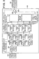
In Bezug auf 2 ist eine ausführliche Beschreibung der Erfassungsschaltung für ein defektes Pixel 105 beschrieben, die ein Signal von einem defekten Pixel im dem Bildsensor 103 mittels Bilddaten erfasst, die durch den Bildsensor 103 und die A/D-Umwandlungsschaltung 104 erzeugt werden. Wie vorstehend erwähnt ist, werden, da der Bildsensor 103 in seinem Inneren eine Bayer-Anordnung von Farbfiltern angeordnet hat, die Bilddaten, die durch den Bildsensor 103 und die A/D-Umwandlungsschaltung 104 erzeugt werden, aus mehreren Arten (3 Arten R, G und B) von einfarbigen Pixelgruppen zusammengesetzt. Es ist anzumerken, dass in dem vorliegenden Ausführungsbeispiel eine Beschreibung abgegeben wird, die das Beispiel eines Falls hernimmt, in dem eines der G-Pixel, das als ein bestimmtes Pixel genommen wird, ein defektes Pixel (Flimmerdefekt) ist.In relation to 2 Fig. 4 is a detailed description of the defective pixel detection circuit 105 described a signal from a defective pixel in the image sensor 103 using image data captured by the image sensor 103 and the A / D conversion circuit 104 are generated. As mentioned above, since the image sensor 103 inside a Bayer array of color filters has arranged the image data through the image sensor 103 and the A / D conversion circuit 104 are generated in several ways ( 3 Types R, G and B) composed of monochrome pixel groups. Note that, in the present embodiment, a description is made taking the example of a case where one of the G pixels taken as a specific pixel is a defective pixel (flicker defect).
Die Erfassungsschaltung für ein defektes Pixel 105 empfängt eine Eingabe von digitalisierten Bilddaten von der A/D-Umwandlungsschaltung 104. Es wird angenommen, dass das Signalniveau jedes Pixels, das in den Bilddaten umfasst ist, durch 8 Bits wiedergegeben wird. Die Erfassungsschaltung für ein defektes Pixel 105 weist eine Nulleinsetzungsschaltung 201, eine erste Tiefpassfilterschaltung (LPF-Schaltung) 202, eine zweite LPF-Schaltung 203, eine dritte LPF-Schaltung 204 und eine vierte LPF-Schaltung 205 auf. Die Erfassungsschaltung für ein defektes Pixel 105 weist ferner eine erste Hochpassfilterschaltung (HPF-Schaltung) 206, eine zweite HPF-Schaltung 207, eine dritte HPF-Schaltung 208 und eine vierte HPF-Schaltung 209 auf. Die Erfassungsschaltung für ein defektes Pixel 105 weist des Weiteren eine erste Absolutschaltung (ABS-Schaltung) 210, eine zweite ABS-Schaltung 211, eine dritte ABS-Schaltung 212 und eine vierte ABS-Schaltung 213 auf. Die Erfassungsschaltung für ein defektes Pixel 105 weist des Weiteren eine Luminanzsignalerzeugungsschaltung 214, eine Defektbestimmungsschaltung 215, eine Grenzwertbestimmungsschaltung (erste Bestimmungseinheit) 216, eine Korrelationsbestimmungsschaltung (zweite Bestimmungseinheit) 217, einen Verstärker (Mulitplizierer) 218 und einen Selektor (Auswahleinrichtung) 219 auf.The defective pixel detection circuit 105 receives an input of digitized image data from the A / D conversion circuit 104. It is assumed that the signal level of each pixel included in the image data is represented by 8 bits. The defective pixel detection circuit 105 has a zero setting circuit 201 , a first low-pass filter circuit (LPF circuit) 202 , a second LPF circuit 203 , a third LPF circuit 204 and a fourth LPF circuit 205 on. The defective pixel detection circuit 105 also has a first high-pass filter circuit (HPF circuit) 206 , a second HPF circuit 207 , a third HPF circuit 208 and a fourth HPF circuit 209 on. The defective pixel detection circuit 105 also has a first absolute circuit (ABS circuit) 210 , a second ABS circuit 211 , a third ABS circuit 212 and a fourth ABS circuit 213 on. The defective pixel detection circuit 105 further includes a luminance signal generating circuit 214 , a defect determination circuit 215 , a limit value determination circuit (first determination unit) 216, a correlation determination circuit (second determination unit) 217, an amplifier (multiplier) 218 and a selector (selector) 219 on.
Die Nulleinsetzungsschaltung 209, die in 3A gezeigt ist, setzt einen Nullwert (0) in die Signalniveaus der Pixel, die von den G-Pixel (Pixel mit verschiedenen Farben von dem bestimmten Pixel) verschieden sind, in einer Region ein, die durch eine Vielzahl von Pixel gebildet ist, deren Zentrum das bestimmte Pixel ist.The zero setting circuit 209 , in the 3A is shown sets a zero value ( 0 ) into the signal levels of the pixels other than the G pixels (pixels with different colors of the particular pixel) in a region formed by a plurality of pixels whose center is the particular pixel.
Die erste LPF-Schaltung 202, die in 3B gezeigt ist, führt eine Tiefpassfilterverarbeitung in der senkrechten Richtung (zum Beispiel eine Tiefpassfilterverarbeitung mittels eines Filterkoeffizienten von (1, 2, 1)) an den Bilddaten aus, in die ein Nullwert in die Signalniveaus der Pixel eingesetzt worden ist, die von den G-Pixel verschieden sind. Dadurch werden die Signalniveaus der Pixel mit einem Nullwert durch die Signalniveaus deren jeweiligen senkrechten Pixel interpoliert.The first LPF circuit 202 , in the 3B low-pass filter processing in the vertical direction (for example, low-pass filter processing using a filter coefficient of (1, 2, 1)) on the image data in which a zero value has been inserted into the signal levels of the pixels used by the G- Pixels are different. As a result, the signal levels of the pixels with a zero value are interpolated by the signal levels of their respective vertical pixels.
Die zweite LPF-Schaltung 203, wie in 3C gezeigt ist, führt eine LPF-Verarbeitung in der waagerechten Richtung an den Bilddaten aus, in denen ein Nullwert in die Signalniveaus der Pixel eingesetzt worden ist, die von den G-Pixel verschieden sind. Dadurch werden die Signalniveaus der Pixel mit einem Nullwert durch die Signalniveaus deren jeweiligen horizontalen Pixel interpoliert.The second LPF circuit 203 , as in 3C is shown performing LPF processing in the horizontal direction on the image data in which a zero value has been inserted into the signal levels of the pixels other than the G pixels. As a result, the signal levels of the pixels with a zero value are interpolated by the signal levels of their respective horizontal pixels.
Die dritte LPF-Schaltung 204, wie in 3D gezeigt ist, führt eine LPF-Verarbeitung in der 135-Grad-Richtung an den Bilddaten aus, in denen ein Nullwert in die Signalniveaus der Pixel eingesetzt worden ist, die von den G-Pixel verschieden sind. Dadurch werden die Signalniveaus der Pixel mit einem Nullwert durch die Signalniveaus deren jeweiligen Pixel interpoliert, die in der 135-Grad-Richtung angeordnet sind. The third LPF circuit 204 , as in 3D is shown performs LPF processing in the 135-degree direction on the image data in which a zero value has been inserted into the signal levels of the pixels other than the G pixels. Thereby, the signal levels of the pixels having a zero value are interpolated by the signal levels of their respective pixels which are arranged in the 135-degree direction.
Die vierte LPF Schaltung 205, wie in 3E gezeigt ist, führte eine LPF-Verarbeitung in der 45-Grad-Richtung an den Bilddaten aus, in denen ein Nullwert in die Signalniveaus der Pixel eingesetzt worden ist, die von den G-Pixel verschieden sind. Dadurch werden die Signalniveaus der Pixel mit einem Nullwert durch die Signalniveaus deren jeweiligen Pixel interpoliert, die in der 45-Grad-Richtung angeordnet sind.The fourth LPF circuit 205 , as in 3E is shown performed LPF processing in the 45-degree direction on the image data in which a zero value has been set in the signal levels of the pixels other than the G pixels. Thereby, the signal levels of the pixels with a zero value are interpolated by the signal levels of their respective pixels, which are arranged in the 45-degree direction.
Die erste HPF-Schaltung 206, wie in 3F gezeigt ist, führt eine Hochpassfilterverarbeitung in der waagerechten Richtung (zum Beispiel eine Hochpassfilterverarbeitung mittels eines Filterkoeffizienten von (-1, 2, -1)) an dem Ergebnis (Ausgabedaten) der LPF-Verarbeitung aus, die durch die erste LPF-Schaltung 204 ausgeführt wird.The first HPF circuit 206 , as in 3F shown, performs high-pass filter processing in the horizontal direction (for example, high-pass filter processing using a filter coefficient of (-1, 2, -1)) on the result (output data) of the LPF processing performed by the first LPF circuit 204 is performed.
Die zweite HPF-Schaltung 207, wie in 3G gezeigt ist, führt eine HPF-Verarbeitung in der senkrechten Richtung an dem Ergebnis (Ausgabedaten) der LPF-Verarbeitung aus, die durch die zweite LPF-Schaltung 203 ausgeführt wird.The second HPF circuit 207 , as in 3G shown performs HPF processing in the vertical direction on the result (output data) of the LPF processing performed by the second LPF circuit 203 is performed.
Die dritte HPF-Schaltung 208, die in 3H gezeigt ist, führt eine HPF-Verarbeitung in der 45-Grad-Richtung an dem Ergebnis (Ausgabedaten) der LPF-Verarbeitung aus, die durch die dritte LPF-Schaltung 204 ausgeführt wird.The third HPF circuit 208 , in the 3H shown performs HPF processing in the 45-degree direction on the result (output data) of the LPF processing performed by the third LPF circuit 204 is performed.
Die vierte HPF-Schaltung 209, wie in 3I gezeigt ist, führt eine HPF-Verarbeitung in der 135-Grad-Richtung an dem Ergebnis (Ausgabedaten) der LPF-Verarbeitung aus, die durch die vierte LPF-Schaltung 205 ausgeführt wird.The fourth HPF circuit 209 , as in 3I HPF processing in the 135 degree direction is performed on the result (output data) of the LPF processing performed by the fourth LPF circuit 205 is performed.
Auf diese Weise bilden in der Erfassungsschaltung für ein defektes Pixel 105, die erste LPF-Schaltung 203 und die erste HPF-Schaltung 206 eine Verarbeitungseinheit zum Ausführen einer Filterverarbeitung in verschiedenen Richtungen mittels des bestimmten Pixels als eine Referenz aus. Auf ähnlicher Weise bilden die zweite LPF-Schaltung 203 und die zweite HPF-Schaltung 204, die dritte LPF-Schaltung 204 und die dritte HPF-Schaltung 208, und die vierte LPF-Schaltung 205 und die vierte HPF-Schaltung 209 ferner jeweils Verarbeitungseinheiten zum Ausführen einer Filterverarbeitung aus. Es ist anzumerken, dass sich die Richtung der LPF-Verarbeitung (erste Richtung) und die Richtung der HPF-Verarbeitung (zweite Richtung orthogonal zu der ersten Richtung) für jede der Verarbeitungseinheiten unterscheiden.In this way, in the detection circuit for a defective pixel 105 , the first LPF circuit 203 and the first HPF circuit 206 a processing unit for performing filter processing in different directions using the determined pixel as a reference. Similarly, form the second LPF circuit 203 and the second HPF circuit 204 , the third LPF circuit 204 and the third HPF circuit 208 , and the fourth LPF circuit 205 and the fourth HPF circuit 209 processing units for executing filter processing. It should be noted that the direction of LPF processing (first direction) and the direction of HPF processing (second direction orthogonal to the first direction) differ for each of the processing units.
Die erste ABS-Schaltung 210 gibt einen 8-Bit Absolutwert des Ergebnisses (Ausgabedaten) der HPF-Verarbeitung aus, die durch die erste HPF-Schaltung 206 ausgeführt wird. Auf ähnliche Weise geben die zweite ABS-Schaltung 211, die dritte ABS-Schaltung 212 und die vierte ABS-Schaltung 213 8-Bit Absolutwerte der Ergebnisse (Ausgabedaten) der HPF-Verarbeitung, die durch die zweite HPF-Schaltung 207, durch die dritte HPF-Schaltung 208 bzw. durch die vierte HPF-Schaltung 209 ausgeführt wird, aus. Die Absolutwerte der Ergebnisse der HPF-Verarbeitung, die durch die erste bis vierte HPF-Schaltung 206 bis 209 ausgeführt wird, werden als HAI, HA2, HA3 bzw. HA4 bezeichnet.The first ABS circuit 210 outputs an 8-bit absolute value of the result (output data) of the HPF processing performed by the first HPF circuit 206 is performed. Similarly give the second ABS circuit 211 , the third ABS circuit 212 and the fourth ABS circuit 213 8-bit absolute values of the results (output data) of the HPF processing by the second HPF circuit 207 , through the third HPF circuit 208 or through the fourth HPF circuit 209 is running out. The absolute values of the results of HPF processing by the first through fourth HPF circuits 206 to 209 are referred to as HAI, HA2, HA3 and HA4, respectively.
Die Luminanzsignalerzeugungsschaltung 214 erzeugt ein Luminanzsignal aus den Bilddaten, die in die Erfassungsschaltung für ein defektes Pixel 105 eingegeben werden (Bilddaten, die aus einer Bayer-Anordnung von R, G und B zusammengesetzt sind). Zum Beispiel erzeugt die Luminanzsignalerzeugungsschaltung 214 ein Luminanzsignal Y in Übereinstimmung mit der nachstehenden Gleichung 1.
The luminance signal generation circuit 214 generates a luminance signal from the image data which is input to the detection circuit for a defective pixel 105 can be entered (image data composed of a Bayer arrangement of R, G and B). For example, the luminance signal generating circuit generates 214 a luminance signal Y in accordance with Equation 1 below.
Die Defektbestimmungsschaltung 215 gibt ein Defektflag, das anzeigt, ob das Signal von dem bestimmten Pixel ein defektes Pixelsignal ist oder nicht, in Übereinstimmung mit den Vorzeichen (plus oder minus) der Ergebnisse der HPF-Verarbeitung aus, die durch die erste bis vierte HPF-Schaltung 206 bis 209 ausgeführt wird. Die Defektbestimmungsschaltung 215 gibt ferner ein Schwarz-und-Weiß-Flag aus, das anzeigt, ob der Defektpixel ein weißer Defekt oder ein schwarzer Defekt ist. Ein „weißer Defekt“ bezieht sich auf ein Defektpixel, das im Dunkeln hell erscheint, und ein „schwarzer Defekt“ bezieht sich auf ein Defektpixel, das unter einfallendem Licht dunkel erscheint.The defect determination circuit 215 outputs a defect flag indicating whether or not the signal from the particular pixel is a defective pixel signal in accordance with the signs (plus or minus) of the results of the HPF processing performed by the first to fourth HPF circuits 206 to 209 is performed. The defect determination circuit 215 also outputs a black-and-white flag indicating whether the defect pixel is a white defect or a black defect. A "white defect" refers to a defect pixel that appears bright in the dark, and a "black defect" refers to a defect pixel that appears dark under incident light.
Insbesondere gibt es in dem Fall, in dem alle Ergebnisse der HPF-Verarbeitung, die durch die erste bis vierte HPF-Schaltung 206 bis 209 ausgeführt wird, dasselbe Vorzeichen haben, die Defektbestimmungsschaltung 215 ein Flag „1“ als das Defektflag aus (1 Bit). Dies zeigt an, dass das Signal von dem bestimmten Pixel ein defektes Pixelsignal ist. Andererseits, gibt in dem Fall, in dem ein beliebiges der Ergebnisse der HPF-Verarbeitung, die durch die erste bis vierte HPF-Schaltung 206 bis 209 ausgeführt wird, ein verschiedenes Vorzeichen hat, die Defektbestimmungsschaltung 215 eine Flag „0“ als das Defektflag aus. Dies zeigt an, dass das Signal von dem bestimmten Pixel nicht ein defektes Pixelsignal ist. In particular, in the case where all the results of the HPF processing by the first to fourth HPF circuit 206 to 209 is executed, have the same sign, the defect determination circuit 215 a flag "1" as the defect flag from (1 bit). This indicates that the signal from the particular pixel is a defective pixel signal. On the other hand, in the case where any of the results of the HPF processing are given by the first to fourth HPF circuits 206 to 209 is executed, has a different sign, the defect determination circuit 215 a flag "0" as that Defect flag off. This indicates that the signal from the particular pixel is not a defective pixel signal.
Es ist anzumerken, dass das Defektflag als ein Auswahlsignal in der Auswahleinrichtung (Selektor) 219 verwendet wird.It should be noted that the defect flag acts as a selection signal in the selector. 219 is used.
In dem Fall, in dem alle Ergebnisse der HPF-Verarbeitung, die durch die erste bis vierte HPF-Schaltung 206 bis 209 ausgeführt wird, ein positives Vorzeichen haben, gibt die Defektbestimmungsschaltung 215 ein Flag „1“, das einen weißen Defekt anzeigt, als das Schwarz-und-Weiß-Flag aus (1 Bit). Andererseits gibt in dem Fall, in dem alle Ergebnisse der HPF-Verarbeitung, die durch die erste bis vierte HPF-Schaltung 206 bis 209 ausgeführt wird, ein negatives Vorzeichen haben, die Defektbestimmungsschaltung 215 ein Flag „0“, das einen schwarzen Defekt anzeigt, als das Schwarz-und-Weiß-Flag aus. Dieses Schwarz-und-Weiß-Flag ist nicht immer notwendig und kann weggelassen werden. Es ist anzumerken, dass das Schwarz-und-Weiß-Flag zu der Grenzwertbestimmungsschaltung 216 ausgegeben wird.In the case where all the results of the HPF processing by the first to fourth HPF circuit 206 to 209 is executed, the defect determination circuit outputs 215 a flag "1" indicating a white defect as the black-and-white flag off (1 bit). On the other hand, in the case where all the results of the HPF processing are given by the first to fourth HPF circuits 206 to 209 is executed, have a negative sign, the defect determination circuit 215 a flag "0" indicating a black defect as the black-and-white flag. This black and white flag is not always necessary and can be omitted. Note that the black and white flag goes to the limit determination circuit 216 is issued.
Die Grenzwertbestimmungsschaltung 216 vergleicht die Absolutwerte HA1 bis HA4 der Ergebnisse der HPF-Verarbeitung, die entsprechend von der ersten bis vierten ABS-Schaltung 210 bis 213 eingegeben worden sind, mit einem beliebig festgelegten Grenzwert. Aufgrund der Grundlage der Vergleichsergebnisse gibt die Grenzwertbestimmungsschaltung 216 einen ersten Bestimmungswert D1 aus, der ein Wert ist, der die Wahrscheinlichkeit anzeigt, dass das Signal von dem bestimmten Pixel ein defektes Pixelsignal ist.The limit determination circuit 216 compares the absolute values HA1 to HA4 the results of the HPF processing, corresponding to the first to fourth ABS circuit 210 to 213 have been entered with an arbitrarily defined limit. Based on the comparison results, the limit determination circuit gives 216 a first determination value D1 which is a value indicating the probability that the signal from the particular pixel is a defective pixel signal.
4 ist ein schematisches Blockschaubild, das die Gestaltung der Grenzwertbestimmungsschaltung 216 zeigt. Die Grenzwertbestimmungsschaltung 216 weist eine erste Defektniveauerzeugungsschaltung 401, eine zweite Defektniveauerzeugungsschaltung 402, eine dritte Defektniveauerzeugungsschaltung 403, eine vierte Defektniveauerzeugungsschaltung 404 und Verstärker (Mulitplizierer) 405 bis 407 auf. 4 Fig. 10 is a schematic block diagram showing the design of the limit determination circuit 216 shows. The limit determination circuit 216 has a first defect level generation circuit 401 , a second defect level generation circuit 402 , a third defect level generation circuit 403 , a fourth defect level generation circuit 404 and amplifiers (multipliers) 405 to 407 on.
Die erste Defektniveauerzeugungsschaltung 401 erzeugt (berechnet) ein Defektniveau DL1 auf der Grundlage des Absolutwerts HA1 des Ergebnisses der HPF-Verarbeitung (Horizontalfilterverarbeitung), der von der ersten ABS-Schaltung 210 eingegeben worden ist. Die zweite Defektniveauerzeugungsschaltung 402 erzeugt ein Defektniveau DL2 auf der Grundlage des Absolutwerts HA2 des Ergebnisses der HPF-Verarbeitung (Vertikalfilterverarbeitung), der von der zweiten ABS-Schaltung 211 eingegeben worden ist. Die dritte Defektniveauerzeugungsschaltung 403 erzeugt ein Defektniveau DL3 auf der Grundlage des Absolutwerts HA3 des Ergebnisses der HPF-Verarbeitung (45-Grad-Filterverarbeitung), der von der dritten ABS-Schaltung 212 eingegeben worden ist. Die vierte Defektniveauerzeugungsschaltung 404 erzeugt ein Defektniveau DL4 auf der Grundlage des Absolutwerts HA4 des Ergebnisses der HPF-Verarbeitung (135-Grad-Filterverarbeitung), der von der vierten ABS-Schaltung 213 eingegeben worden ist. Es wird angenommen, dass diese Absolutwerte HA1 bis HA4 der Ergebnisse der HPF-Verarbeitung jeweils durch einen 8-Bit Wert wiedergegeben werden.The first defect level generation circuit 401 generates (calculates) a defect level DL1 based on the absolute value HA1 the result of the HPF processing (horizontal filter processing) by the first ABS circuit 210 has been entered. The second defect level generation circuit 402 creates a defect level DL2 based on the absolute value HA2 the result of the HPF processing (vertical filter processing) by the second ABS circuit 211 has been entered. The third defect level generation circuit 403 creates a defect level DL3 based on the absolute value HA3 the result of the HPF processing (45 degree filter processing) by the third ABS circuit 212 has been entered. The fourth defect level generation circuit 404 creates a defect level DL4 based on the absolute value HA4 the result of the HPF processing (135 degree filter processing) by the fourth ABS circuit 213 has been entered. It is believed that these are absolute values HA1 to HA4 the results of the HPF processing are each represented by an 8-bit value.
Eine ausführliche Beschreibung der Erzeugung des Defektniveaus, die durch die erste bis vierte Defektniveauerzeugungsschaltung 401 bis 404 ausgeführt wird, ist mit Bezug auf 5A und 5B gezeigt. Es ist anzumerken, dass sich der Begriff „Defektniveau“, der nachstehend verwendet wird, auf einen Wert bezieht, der die Wahrscheinlichkeit anzeigt, dass das Signal von dem bestimmten Pixel ein defektes Pixelsignal ist. In dem vorliegenden Ausführungsbeispiel wird das Defektniveau als ein Wert erzeugt, der von 0 bis 255 reicht, wobei das Defektniveau „0“ anzeigt, dass das Signal von dem bestimmten Pixel nicht ein defektes Pixelsignal ist. Im Gegensatz dazu zeigt das Defektniveau „255“ an, dass das Signal von dem bestimmten Pixel ein defektes Pixelsignal ist. Je näher das Defektniveau an „0“ liegt, desto höher ist die Wahrscheinlichkeit, dass das Signal von dem bestimmten Pixel nicht ein defektes Pixelsignal ist, wohingegen, je näher das Defektniveau an „255“ liegt, desto höher ist die Wahrscheinlichkeit, dass das Signal von dem bestimmten Pixel ein defektes Pixelsignal ist.A detailed description of the generation of the defect level by the first to fourth defect level generation circuits 401 to 404 is executed with reference to 5A and 5B shown. It should be noted that the term “defect level” used below refers to a value that indicates the probability that the signal from the particular pixel is a defective pixel signal. In the present embodiment, the defect level is generated as a value ranging from 0 to 255, the defect level "0" indicating that the signal from the particular pixel is not a defective pixel signal. In contrast, the defect level "255" indicates that the signal from the particular pixel is a defective pixel signal. The closer the defect level is to "0", the higher the probability that the signal from the particular pixel is not a defective pixel signal, whereas the closer the defect level is to "255", the higher the probability that the signal is is a defective pixel signal from the particular pixel.
5A und 5B zeigen das Verhältnis zwischen dem Absolutwert des Ergebnisses der HPF-Verarbeitung, der zu der ersten bis vierten Defektniveauerzeugungsschaltung 401 bis 404 eingegeben wird, und dem Defektniveau (Wert), der durch die erste bis vierte Defektniveauerzeugungsschaltung 401 bis 404 erzeugt wird. In 5A und 5B zeigt die waagerechte Achse den Absolutwert HA (HA1 bis HA4) als das Ergebnis der HPF-Verarbeitung an und zeigt die senkrechte Achse das Defektniveau DL (DL1 bis DL4) an. 5A and 5B show the relationship between the absolute value of the result of the HPF processing to the first to fourth defect level generation circuits 401 to 404 is entered, and the defect level (value) by the first to fourth defect level generation circuits 401 to 404 is produced. In 5A and 5B the horizontal axis shows the absolute value HA ( HA1 to HA4 ) as the result of HPF processing and the vertical axis shows the defect level DL ( DL1 to DL4 ) on.
Die erste bis vierte Defektniveauerzeugungsschaltungen 401 bis 404 halten im Voraus einen Grenzwert TH2, der in 5A und 5B gezeigt ist, und einen Steigungswert SL1. Die erste bis vierte Defektniveauerzeugungsschaltungen 401 bis 404 wandeln den Absolutwert HA des Ergebnisses der HPF-Verarbeitung in das Defektniveau DL (8 Bits) in Übereinstimmung mit den nachstehenden Gleichungen 2 bis 4 um.The first to fourth defect level generation circuits 401 to 404 keep a limit in advance TH2 who in 5A and 5B and a slope value SL1 , The first to fourth defect level generation circuits 401 to 404 convert the absolute value HA of the result of the HPF processing into the defect level DL ( 8th Bits) in accordance with Equations 2 to 4 µm below.
In dem Fall, in dem HA ≤ TH2 ist,
In the case where HA ≤ TH2 is
In dem Fall, in dem TH2 < HA < TH1 ist,
In the case where TH2 <HA <TH1,
In dem Fall, in dem TH1 ≤ HA ist,
In the case where TH1 ≤ HA,
Hier gilt TH1 = TH2 + (255/SL1).Applies here TH1 = TH2 + (255 / SL1).
Zum Beispiel erzeugen in den Beispielen, in den 5A und 5B gezeigt sind, wenn der Eingabeabsolutwert HA des Ergebnisses der HPF-Verarbeitung größer ist als oder gleich ist wie ein Grenzwert, die erste bis vierte Defektniveauerzeugungsschaltung 401 bis 404 das Defektniveau DL von „255“. Andererseits erzeugen, wenn der Eingabeabsolutwert HA des Ergebnisses der HPF-Verarbeitung kleiner ist als oder gleich ist wie der Grenzwert TH2, die erste bis vierte Defektniveauerzeugungsschaltung 401 bis 404 das Defektniveau DL von „0“. Wenn der Eingabeabsolutwert HA des Ergebnisses der HPF-Verarbeitung größer ist als der Grenzwert TH2 und kleiner ist als der Grenzwert TH1, erzeugen die erste bis vierte Defektniveauerzeugungsschaltung 401 bis 404 das Defektniveau DL eines Werts, der sich erhöht, wenn sich der Eingabeabsolutwert des Ergebnisses der HPF-Verarbeitung erhöht.For example, generate in the examples in the 5A and 5B are shown, when the input absolute value HA of the result of the HPF processing is greater than or equal to a limit value, the first through fourth defect level generation circuits 401 to 404 the defect level DL of "255". On the other hand, generate if the input absolute value HA of the result of the HPF processing is less than or equal to the limit value TH2 , the first to fourth defect level generation circuits 401 to 404 the defect level DL of "0". When the input absolute value HA of the result of the HPF processing is larger than the limit value TH2 and is less than the limit TH1 , generate the first to fourth defect level generation circuits 401 to 404 the defect level DL of a value that increases as the input absolute value of the result of the HPF processing increases.
Es ist anzumerken, dass die erste bis vierte Defektniveauerzeugungsschaltung 401 bis 404 den Grenzwert TH1 und die Steigung SL1 in Übereinstimmung mit der Eingabe des Schwarz-und-Weiß-Flags von der Defektbestimmungsschaltung 215 ändern, d.h. abhängig davon, ob das defekte Pixel ein weißer Defekt oder ein schwarzer Defekt ist. Zum Beispiel legen, wenn das defekte Pixel ein weißer Defekt ist, die erste bis vierte Defekterfassungserzeugungsschaltung 401 bis 404 den Grenzwert TH2 und die Steigung SL1 derart fest, um eine Charakteristik aufzuweisen, wie in 5A gezeigt ist, wohingegen, wenn das defekte Pixel ein schwarzer Defekt ist, die erste bis vierte Defektniveauerzeugungsschaltung 401 bis 404 den Grenzwert TH2 und die Steigung SL1 derart festlegen, um die Charakteristik aufzuweisen, wie in 5B gezeigt ist.Note that the first to fourth defect level generation circuits 401 to 404 the limit TH1 and the slope SL1 in accordance with the input of the black and white flag from the defect determination circuit 215 change, ie depending on whether the defective pixel is a white defect or a black defect. For example, if the defective pixel is a white defect, put the first through fourth defect detection generation circuits 401 to 404 the limit TH2 and the slope SL1 so firm to have a characteristic as in 5A is shown, whereas if the defective pixel is a black defect, the first to fourth defect level generating circuits 401 to 404 the limit TH2 and the slope SL1 set in such a way to have the characteristic as in 5B is shown.
Es wird angenommen, dass der Grenzwert TH2 ein Wert ist, der durch Multiplizieren eines beliebig festgelegten Werts, der durch den Betriebsmodus des Abbildungsgeräts 100 zum Beispiel bestimmt ist, und eines Durchschnittswerts der Luminanzsignale von den benachbarten Pixel des bestimmten Pixels bestimmt wird, die durch die Luminanzsignalerzeugungsschaltung 214 erzeugt werden. Es ist erforderlich, dass sich der Grenzwert TH2 in Übereinstimmung mit den Luminanzsignalen ändert, die durch die Luminanzsignalerzeugungsschaltung 214 erzeugt werden (d.h., dem Ausmaß des Rauschens), da, je höher die Luminanz ist, desto größer ist das Rauschen. Durch Erhöhen des Grenzwerts TH2, wenn sich die Luminanz erhöht, ist es möglich, zu verhindern, dass ein Rauschen fehlerhaft als ein defektes Pixel beurteilt wird. Es wird ferner angenommen, dass die Steigung SL1 auch ein Wert ist, der durch Multiplizieren eines beliebig festgelegten Werts, der zum Beispiel durch den Betriebsmodus des Abbildungsgeräts 100 bestimmt wird, und der Luminanzsignale, die durch die Luminanzsignalerzeugungsschaltung 214 erzeugt werden, erhalten werden. Der Grenzwert TH1 wird durch Bestimmen des Grenzwerts TH2 und der Steigung SL1 bestimmt. Es ist anzumerken, dass das Defektniveau DL relativ zu dem Absolutwert HA, wie in 5A und 5B gezeigt ist, in einer Tabelle vorgespeichert werden kann, anstelle dass es durch Umwandlung mittels den Gleichungen 2 bis 4 erhalten wird. It is assumed that the limit TH2 is a value obtained by multiplying an arbitrarily set value by the operating mode of the imaging device 100 for example, and an average value of the luminance signals from the neighboring pixels of the particular pixel is determined by the luminance signal generation circuit 214 be generated. It is required that the limit TH2 in accordance with the luminance signals changed by the luminance signal generation circuit 214 are generated (ie, the amount of noise) because the higher the luminance, the greater the noise. By increasing the limit TH2 If the luminance increases, it is possible to prevent noise from being misjudged as a defective pixel. It is also assumed that the slope SL1 is also a value obtained by multiplying an arbitrarily determined value, for example, by the operating mode of the imaging device 100 and the luminance signals generated by the luminance signal generating circuit 214 generated, obtained. The limit TH1 is determined by determining the limit TH2 and the slope SL1 certainly. It should be noted that the defect level DL relative to the absolute value HA , as in 5A and 5B is shown, can be pre-stored in a table instead of being obtained by conversion using equations 2-4.
Alternativ kann anstelle des Festlegens der Grenzwerte TH1 und TH2 das Verhältnis zwischen dem Absolutwert HA und dem Defektniveau DL als eine Funktion (z.B. als eine kubische Funktion) definiert sein, in der sich das Defektniveau DL erhöht, wenn sich der Absolutwert HA erhöht, über den gesamten Bereich des Absolutwerts HA. Dann kann diese Funktion in Übereinstimmung mit der Luminanz umgeschaltet werden, so dass sich der Wert des Defektniveaus DL relativ zu dem Absolutwert HA verringert, wenn sich die Luminanz in der Umgebung des bestimmten Pixels erhöht.Alternatively, instead of setting the limit values TH1 and TH2 the ratio between the absolute value HA and the defect level DL be defined as a function (eg as a cubic function) in which the defect level DL increases when the absolute value HA increased over the entire range of the absolute value HA , Then this function can be switched in accordance with the luminance, so that the value of the defect level DL relative to the absolute value HA decreases as the luminance increases in the vicinity of the particular pixel.
Der Verstärker 405 erhält einen 16-Bit Wert durch Multiplizieren des Defektniveaus, das durch die erste Defektniveauerzeugungsschaltung 401 erzeugt wird, und des Defektniveaus, das durch die zweite Defektniveauerzeugungsschaltung 402 erzeugt wird, führt einen 8-Bit Veränderungsbetrieb an dem 16-Bit Wert aus und gibt den sich ergebenden 8-Bit Wert als ein Defektniveau DL5 aus. Der Verstärker 406 erhält einen 16-Bit Wert durch Multiplizieren des Defektniveaus, das durch die dritte Defektniveauerzeugungsschaltung 403 erzeugt wird, und des Defektniveaus, das durch die vierte Defektniveauerzeugungsschaltung 404 erzeugt wird, führt einen 8-Bit Veränderungsbetrieb an dem 16-Bit Wert aus und gibt den sich ergebenden 8-Bit Wert als ein Defektniveau DL6 aus. Der Verstärker 407 erhält einen 16-Bit Wert durch Multiplizieren des Defektniveaus DL5, das durch die Multiplikation durch den Verstärker 405 erhalten wird, und des Defektniveaus DL6, das durch die Multiplikation durch den Verstärker 406 erhalten wird, führt einen 8-Bit Veränderungsbetrieb an dem 16-Bit Wert aus und gibt den sich ergebenden 8-Bit Wert als einen ersten Bestimmungswert D1 aus.The amplifier 405 obtains a 16-bit value by multiplying the defect level by the first defect level generation circuit 401 and the level of defects generated by the second level of defect generation circuit 402 is generated, performs an 8-bit change operation on the 16-bit value and outputs the resulting 8-bit value as a defect level DL5 out. The amplifier 406 obtains a 16-bit value by multiplying the defect level by the third defect level generation circuit 403 and the defect level generated by the fourth defect level generation circuit 404 is generated, performs an 8-bit change operation on the 16-bit value and outputs the resulting 8-bit value as a defect level DL6 out. The amplifier 407 receives a 16-bit value by multiplying the defect level DL5 that by multiplying by the amplifier 405 is obtained, and the level of defects DL6 that by multiplying by the amplifier 406 is obtained, performs an 8-bit change operation on the 16-bit value and outputs the resulting 8-bit value as a first determination value D1 out.
Auf diese Weise erhält die Grenzwertbestimmungsschaltung 216 auf der Grundlage der Ergebnisse der Filterverarbeitung eine Differenz des Signalniveaus zwischen dem bestimmten Pixel und einer Vielzahl von Pixel, die in der Umgebung des bestimmten Pixels angeordnet sind. Die Grenzwertbestimmungsschaltung 216 erzeugt dann den ersten Bestimmungswert D1, der anzeigt, dass, je höher die Differenz ist, desto höher ist die Wahrscheinlichkeit, dass das Signal von dem bestimmten Pixel ein defektes Pixelsignal ist.In this way, the limit value determination circuit receives 216 on the basis of Filter processing results in a difference in signal level between the particular pixel and a plurality of pixels located in the vicinity of the particular pixel. The limit determination circuit 216 then generates the first determination value D1 , which indicates that the higher the difference, the higher the likelihood that the signal from the particular pixel is a defective pixel signal.
Bezogen auf 2 vergleicht die Korrelationsbestimmungsschaltung 217 die Stärken der Absolutwerte HA1 bis HA4 der Ergebnisse der HPF-Verarbeitung, die entsprechend von der ersten bis vierten ABS-Schaltung 210 bis 213 eingegeben worden sind. Auf der Grundlage des Vergleichsergebnisses gibt die Korrelationsbestimmungsschaltung 217 einen zweiten Bestimmungswert D2 aus, der die Wahrscheinlichkeit anzeigt, dass das Signal von dem bestimmten Pixel ein defektes Pixelsignal ist.Related to 2 compares the correlation determination circuit 217 the strengths of the absolute values HA1 to HA4 the results of the HPF processing, corresponding to the first to fourth ABS circuit 210 to 213 have been entered. Based on the comparison result, the correlation determination circuit gives 217 a second determination value D2 indicating the probability that the signal from the particular pixel is a defective pixel signal.
6 ist ein schematisches Blockschaubild, das die Gestaltung der Korrelationsbestimmungsschaltung 217 zeigt. Die Korrelationsbestimmungsschaltung 217 weist eine erste Auswahlschaltung 601, eine zweite Auswahlschaltung 602, eine dritte Auswahlschaltung 603, eine vierte Auswahlschaltung 604, eine fünfte Auswahlschaltung 605, eine sechste Auswahlschaltung 606, eine Subtraktionseinrichtung 607 und eine Defektniveaubestimmungsschaltung 608 auf. 6 Fig. 3 is a schematic block diagram showing the configuration of the correlation determination circuit 217 shows. The correlation determination circuit 217 has a first selection circuit 601 , a second selection circuit 602 , a third selection circuit 603 , a fourth selection circuit 604 , a fifth selection circuit 605 , a sixth selection circuit 606 , a subtraction device 607 and a defect level determination circuit 608 on.
Die erste Auswahlschaltung 601 vergleicht den Absolutwert HA1 des Ergebnisses der HPF-Verarbeitung, der von der ersten ABS-Schaltung 210 eingegeben worden ist, und den Absolutwert HA2 des Ergebnisses der HPF-Verarbeitung, der von der zweiten ABS-Schaltung 211 eingegeben worden ist, und gibt den größeren Absolutwert aus. Die zweite Auswahlschaltung 602 vergleicht den Absolutwert HA1 des Ergebnisses der HPF-Verarbeitung, der von der ersten ABS-Schaltung 210 eingegeben worden ist, und den Absolutwert HA2 des Ergebnisses der HPF-Verarbeitung, der von der zweiten ABS-Schaltung 211 eingegeben worden ist, und gibt den kleineren Absolutwert aus.The first selection circuit 601 compares the absolute value HA1 the result of HPF processing from the first ABS circuit 210 has been entered and the absolute value HA2 the result of HPF processing from the second ABS circuit 211 has been entered and outputs the larger absolute value. The second selection circuit 602 compares the absolute value HA1 the result of HPF processing from the first ABS circuit 210 has been entered and the absolute value HA2 the result of HPF processing from the second ABS circuit 211 has been entered and outputs the smaller absolute value.
Die dritte Auswahlschaltung 603 vergleicht den Absolutwert HA3 des Ergebnisses der HPF-Verarbeitung, der von der dritten ABS-Schaltung 212 eingegeben worden ist, und den Absolutwert HA4 des Ergebnisses der HPF-Verarbeitung, der von der vierten ABS-Schaltung 213 eingegeben worden ist, und gibt den größeren Absolutwert aus. Die vierte Auswahlschaltung 604 vergleicht den Absolutwert HA3 des Ergebnisses der HPF-Verarbeitung, der von der dritten ABS-Schaltung 212 eingegeben worden ist, und den Absolutwert HA4 des Ergebnisses der HPF-Verarbeitung, der von der vierten ABS-Schaltung 413 eingegeben worden ist, und gibt den kleineren Absolutwert aus.The third selection circuit 603 compares the absolute value HA3 the result of the HPF processing by the third ABS circuit 212 has been entered and the absolute value HA4 the result of the HPF processing by the fourth ABS circuit 213 has been entered and outputs the larger absolute value. The fourth selection circuit 604 compares the absolute value HA3 the result of the HPF processing by the third ABS circuit 212 has been entered and the absolute value HA4 the result of the HPF processing by the fourth ABS circuit 413 has been entered and outputs the smaller absolute value.
Die fünfte Auswahlschaltung 605 vergleicht den Absolutwert, der von der ersten Auswahlschaltung 601 ausgegeben wird, und den Absolutwert, der von der dritten Auswahlschaltung 603 ausgegeben wird, und gibt den größeren Absolutwert aus. Der Absolutwert, der von der fünften Auswahlschaltung 605 ausgegeben wird, ist ein maximaler Absolutwert aus den Ergebnissen der HPF-Verarbeitung, die durch die erste bis vierte ABS-Schaltung 210 bis 213 ausgeführt wird (d.h. aus den Ergebnissen der Filterverarbeitung, die in den vier Richtungen ausgeführt wird.)The fifth selection circuit 605 compares the absolute value from the first selection circuit 601 is output, and the absolute value given by the third selection circuit 603 is output and outputs the larger absolute value. The absolute value by the fifth selection circuit 605 is output is a maximum absolute value from the results of the HPF processing by the first to fourth ABS circuits 210 to 213 is executed (that is, from the results of filter processing performed in the four directions.)
Die sechste Auswahlschaltung 606 vergleicht den Absolutwert, der von der zweiten Auswahlschaltung 602 ausgegeben wird, und den Absolutwert, der von der vierten Auswahlschaltung 604 ausgegeben wird, und gibt den kleineren Absolutwert aus. Der Absolutwert, der von der sechsten Auswahlschaltung 606 ausgegeben wird, ist ein minimaler Absolutwert aus den Ergebnissen der HPF-Verarbeitung, die durch die erste bis vierte ABS-Schaltung 210 bis 213 ausgeführt wird (d.h. aus den Ergebnissen der Filterverarbeitung, die in den vier Richtungen ausgeführt wird).The sixth selection circuit 606 compares the absolute value from the second selection circuit 602 is output, and the absolute value given by the fourth selection circuit 604 is output and outputs the smaller absolute value. The absolute value from the sixth selection circuit 606 is output is a minimum absolute value from the results of HPF processing by the first through fourth ABS circuits 210 to 213 is carried out (ie from the results of filter processing carried out in the four directions).
Die Subtrahiereinrichtung 607 subtrahiert den Absolutwert, der von der sechsten Auswahlschaltung 606 ausgegeben wird, von dem Absolutwert, der von der fünften Auswahlschaltung 605 ausgegeben wird. Das Ergebnis der Subtraktion, die durch die Subtrahiereinrichtung 607 ausgeführt wird, zeigt eine maximale Differenz (die Verteilungsbreite der Differenz) aus den Ergebnissen der HPF-Verarbeitung an, die durch die erste bis vierte ABS-Schaltung 210 bis 213 ausgeführt wird, und wird immer ein positiver Wert sein, der größer ist als oder gleich wie null, da sie durch Subtrahieren des minimalen absoluten Werts von dem maximalen absoluten Wert erhalten wird.The subtractor 607 subtracts the absolute value from the sixth selection circuit 606 is output from the absolute value by the fifth selection circuit 605 is issued. The result of subtraction by the subtractor 607 executed indicates a maximum difference (the distribution width of the difference) from the results of the HPF processing performed by the first to fourth ABS circuits 210 to 213 and will always be a positive value greater than or equal to zero since it is obtained by subtracting the minimum absolute value from the maximum absolute value.
Die Defektniveaubestimmungsschaltung 608 erzeugt (berechnet) den zweiten Bestimmungswert D2 auf der Grundlage des Absolutwerts, der von der Subtrahiereinrichtung 607 ausgegeben wird, und gibt den zweiten Bestimmungswert D2 aus. Eine spezifische Beschreibung der Erzeugung des zweiten Bestimmungswerts D2, die durch die Defektniveaubestimmungsschaltung 608 ausgeführt wird, ist mit Bezug auf 7 gegeben. Es ist anzumerken, dass ähnlich wie der erste Bestimmungswert D1 der zweite Bestimmungswert D2, der durch die Defektniveaubestimmungsschaltung 608 erzeugt wird, die Wahrscheinlichkeit des Signals von dem bestimmten Pixel anzeigt, dass es ein defektes Pixelsignal ist. 7 ist ein Schaubild, das das Verhältnis zwischen dem Ergebnis der Subtraktion (Absolutwert HB), die durch die Subtrahiereinrichtung 607 ausgeführt wird, das (der) zu der Defektniveaubestimmungsschaltung 608 einzugeben ist, und dem zweiten Bestimmungswert D2 zeigt, der durch die Defektniveaubestimmungsschaltung 608 erzeugt wird. In 7 zeigt die waagerechte Achse das Ergebnis der Subtraktion (Absolutwert HB) an, die durch die Subtrahiereinrichtung 607 ausgeführt wird, und zeigt die senkrechte Achse den zweiten Bestimmungswert D2 an.The defect level determination circuit 608 generates (calculates) the second determination value D2 based on the absolute value obtained from the subtractor 607 is output and returns the second determination value D2 out. A specific description of the generation of the second determination value D2 by the defect level determination circuit 608 is executed with reference to 7 given. It should be noted that similar to the first determination value D1 the second determination value D2 by the defect level determination circuit 608 is generated, the probability of the signal from the particular pixel indicates that it is a defective pixel signal. 7 is a graph showing the relationship between the result of subtraction (absolute value HB) by the subtractor 607 that is to the defect level determination circuit 608 is to be entered, and the second determination value D2 shows that by the defect level determination circuit 608 is produced. In 7 the horizontal axis shows the result of the subtraction (absolute value HB) by the subtractor 607 is executed, and the vertical axis shows the second determination value D2 on.
Die Defektniveaubestimmungsschaltung 608 hält im Voraus einen Grenzwert TH3 und einen Steigungswert SL2, die in 7 gezeigt sind, und wandelt das Ergebnis der Subtraktion durch die Subtrahiereinrichtung 607 in einen zweiten Bestimmungswert D2 (8 Bits) in Übereinstimmung mit den nachstehenden Gleichungen 5 bis 7 um.The defect level determination circuit 608 holds a limit in advance TH3 and a slope value SL2 , in the 7 and converts the result of the subtraction by the subtractor 607 into a second determination value D2 (8 bits) in accordance with Equations 5 through 7 µm below.
In dem Fall, in dem HP ≤ TH3 ist,
In the case where HP ≤ TH3,
In dem Fall, in dem TH3 < HB < TH4 ist,
In the case where TH3 <HB <TH4,
In dem Fall, in dem TH4 ≤ HB ist,
In the case where TH4 ≤ HB,
Hier gilt TH4 = TH3 - (255/SL2).Here TH4 = TH3 - (255 / SL2) applies.
Zum Beispiel erzeugt in dem Beispiel, das in 7 gezeigt ist, wenn das Ergebnis HB der Subtraktion durch die Subtrahiereinrichtung 607 kleiner ist als oder gleich ist wie der Grenzwert TH3, die Defektniveaubestimmungsschaltung 608 den zweiten Bestimmungswert D2 mit „255“. Andererseits erzeugt, wenn das Ergebnis HB der Subtraktion durch die Subtrahiereinrichtung 607 größer ist als oder gleich ist wie der Grenzwert TH4, die Defektniveaubestimmungsschaltung 608 den zweiten Bestimmungswert D2 mit „0“. Wenn das Ergebnis HB der Subtraktion durch die Subtrahiereinrichtung 607 größer ist als der Grenzwert TH3 und kleiner ist als der Grenzwert TH4, erzeugt die Defektniveaubestimmungsschaltung 608 den zweiten Bestimmungswert D2 mit einem Wert, der sich erhöht, wenn sich das Ergebnis der Subtraktion durch die Subtrahiereinrichtung 607 (Absolutwert) verringert.For example, in the example created in 7 is shown when the result HB of the subtraction by the subtractor 607 is less than or equal to the limit TH3 who have favourited Defect Level Determination Circuit 608 the second determination value D2 with "255". On the other hand, if the result HB is generated by the subtraction by the subtractor 607 is greater than or equal to the limit TH4 who have favourited Defect Level Determination Circuit 608 the second determination value D2 with "0". If the result HB of the subtraction by the subtractor 607 is greater than the limit TH3 and is less than the limit TH4 , generates the defect level determination circuit 608 the second determination value D2 with a value that increases as the result of the subtraction by the subtractor 607 (Absolute value) decreased.
Es ist anzumerken, dass der Grenzwert TH3 ein Wert ist, der durch Multiplizieren eines beliebig festgelegten Werts, der zum Beispiel durch den Betriebsmodus des Abbildungsgeräts 100 bestimmt wird, und des Luminanzsignals erhalten wird, das durch die Luminanzsignalerzeugungsschaltung 214 erzeugt wird. Es ist ferner anzumerken, dass die Steigung SL2 auch ein Wert ist, der durch Multiplizieren eines beliebig festgelegten Werts, der zum Beispiel durch den Betriebsmodus des Abbildungsgeräts 100 festgelegt ist, und des Luminanzsignals erhalten wird, das durch die Luminanzsignalerzeugungsschaltung 214 erzeugt wird. Der Grenzwert TH4 wird durch Bestimmen des Grenzwerts TH3 und des Steigungswerts SL2 bestimmt. Alternativ kann der zweite Bestimmungswert D2 relativ zu dem Ergebnis HB der Subtraktion durch die Subtrahiereinrichtung 607, die in 7 gezeigt ist, in einer Tabelle vorab gespeichert sein, anstelle dass er durch Umwandlung mittels den Gleichungen 5 bis 7 erhalten wird.It should be noted that the limit TH3 is a value obtained by multiplying an arbitrarily set value, for example, by the mode of operation of the imaging device 100 is determined, and the luminance signal is obtained by the luminance signal generating circuit 214 is produced. It should also be noted that the slope SL2 is also a value obtained by multiplying an arbitrarily determined value, for example, by the operating mode of the imaging device 100 is fixed, and the luminance signal is obtained by the luminance signal generating circuit 214 is produced. The limit TH4 is determined by determining the limit TH3 and the slope value SL2 certainly. Alternatively, the second determination value D2 relative to the result HB of the subtraction by the subtractor 607 , in the 7 is stored in a table in advance, instead of being obtained by conversion using equations 5 through 7.
Auf diese Weise erhält die Korrelationsbestimmungsschaltung 217 auf der Grundlage der Ergebnisse der Filterverarbeitung die Verteilungsbreite der Differenz des Signalniveaus zwischen dem bestimmten Pixel und den benachbarten Pixel des bestimmten Pixels (d.h. das Subtraktionsergebnis HB). Die Korrelationsbestimmungsschaltung 217 erzeugt dann den zweiten Bestimmungswert D2, der anzeigt, dass, je kleiner die vorstehende Verteilungsbreite der Differenz ist, desto größer ist die Wahrscheinlichkeit, dass das Signal von dem bestimmten Pixel ein defektes Pixelsignal ist.In this way, the correlation determination circuit obtains 217 based on the results of filter processing, the distribution width of the difference in signal level between the particular pixel and the neighboring pixels of the particular pixel (ie, the subtraction result HB). The correlation determination circuit 217 then generates the second determination value D2 , which indicates that the smaller the above distribution width of the difference, the greater the likelihood that the signal from the particular pixel is a defective pixel signal.
Es ist anzumerken, dass in dem Fall, in dem ein starkes Rauschen in den Bilddaten umfasst ist, es wahrscheinlich sein kann, dass die Grenzwertbestimmungsschaltung 216 das Signal von dem bestimmten Pixel als ein defektes Pixelsignal (d.h. Ausgabe des ersten Bestimmungswerts beträgt „255“) aufgrund des Rauschens fehlerhaft beurteilen kann. In Anbetracht dessen ist es bei der Korrelationsbestimmungsschaltung 217 erforderlich, dass das Signal von dem bestimmten Pixel nicht als ein defektes Pixelsignal in dem Fall bestimmt wird, in dem ein starkes Rauschen in den Bilddaten einer Region einschließlich des bestimmten Pixels umfasst ist und ferner die Verteilungsbreite der Differenz groß ist.Note that in the case where there is a lot of noise in the image data, it may be likely that the limit determination circuit 216 can misjudge the signal from the determined pixel as a defective pixel signal (ie, output of the first determination value is "255") due to the noise. In view of this, it is with the correlation determination circuit 217 required that the signal from the designated pixel is not determined as a defective pixel signal in the case where there is a lot of noise in the image data of a region including the designated pixel and further the distribution width of the difference is large.
In dem Fall, in dem das bestimmte Pixel nicht ein defektes Pixel ist, sind die Ergebnisse der HPF-Verarbeitung, die durch die erste bis vierte ABS-Schaltung 210 bis 213 erhalten werden (d.h. die Ergebnisse der Filterverarbeitung, die in vier Richtungen ausgeführt wird), ein Wert nahe null, und demgemäß ist die Verteilungsbreite der Differenzen auch ein Wert nahe null. In einem derartigen Fall kann die Korrelationsbestimmungsschaltung 217 das Signal von dem bestimmten Pixel als ein defektes Pixelsignal (d.h., eine Ausgabe des zweiten Bestimmungswerts beträgt „255“) fehlerhaft beurteilen, da die Verteilungsbreite der Differenzen gering ist. Aus diesem Grund ist es bei der Grenzwertbestimmungsschaltung 216 erforderlich, das Signal von dem bestimmten Pixel als ein defektes Pixelsignal in dem Fall zu bestimmen, in dem die Differenz des Signalniveaus zwischen dem bestimmten Pixel und dem benachbarten Pixel größer ist als oder gleich ist wie ein Grenzwert.In the case where the particular pixel is not a defective pixel, the results of the HPF processing are by the first through fourth ABS circuits 210 to 213 are obtained (ie, the results of filter processing performed in four directions) a value close to zero, and accordingly the distribution width of the differences is also a value close to zero. In such a case, the correlation determination circuit can 217 misjudge the signal from the determined pixel as a defective pixel signal (ie, an output of the second determination value is "255") because the spread of the differences is narrow. For this reason, it is the limit determination circuit 216 required to determine the signal from the particular pixel as a defective pixel signal in the case where the difference of the Signal levels between the particular pixel and the neighboring pixel is greater than or equal to a threshold.
In Anbetracht dieses Zusammenhangs erhält in dem vorliegenden Ausgangsbeispielen, wie in 2 gezeigt ist, der Verstärker 218 einen dritten Bestimmungswert durch Multiplizieren des ersten Bestimmungswerts D1, der von der Grenzwertbestimmungsschaltung 216 ausgegeben wird, und des zweiten Bestimmungswerts D2, der von der Korrelationsbestimmungsschaltung 217 ausgegeben wird. Insbesondere erhält der Verstärker 218 einen 16-Bit Wert durch Multiplizieren des ersten Bestimmungswerts D1 und des zweiten Bestimmungswerts D2, führt einen 8-Bit Veränderungsbetrieb an dem 16-Bit Wert aus und gibt den sich ergebenden 8-Bit Wert (d.h. den Wert von 0 bis 255) als einen dritten Bestimmungswert K aus. Dies ermöglicht es, dass die Korrelationsbestimmungsschaltung 217 geeignet bestimmen kann, ob das bestimmte Pixel ein defektes Pixel ist oder nicht, selbst wenn die Grenzwertbestimmungsschaltung 216 eine Fehlbeurteilung gemacht hat, und ermöglicht es, dass die Grenzwertbestimmungsschaltung 216 geeignet bestimmen kann, ob das bestimmte Pixel ein defektes Pixel ist, selbst wenn die Korrelationsbestimmungsschaltung 217 eine Fehlbeurteilung gemacht hat. In anderen Worten wird sowohl bei der Grenzwertbestimmungsschaltung 216 als auch der Korrelationsbestimmungsschaltung 217, wenn das bestimmte Pixel als ein defektes Pixel bestimmt worden ist, das bestimmte Pixel als ein defektes Pixel erfasst. Alternativ wird sowohl bei der Grenzwertbestimmungsschaltung 216 als auch der Korrelationsbestimmungsschaltung 217, wenn es bestimmt worden ist, dass es eine hohe Wahrscheinlichkeit gibt, dass das bestimmte Pixel ein defektes Pixel ist, das Signal von dem bestimmten Pixel als ein Signal erfasst, das ein defektes Pixelsignal sehr wahrscheinlich ist.In view of this connection, in the present starting examples, as in 2 is shown the amplifier 218 a third determination value by multiplying the first determination value D1 by the limit value determination circuit 216 is output, and the second determination value D2 by the correlation determination circuit 217 is issued. In particular, the amplifier receives 218 a 16-bit value by multiplying the first determination value D1 and the second determination value D2 , performs an 8-bit change operation on the 16-bit value and outputs the resulting 8-bit value (ie, the value from 0 to 255) as a third determination value K. This enables the correlation determination circuit 217 can appropriately determine whether or not the particular pixel is a defective pixel even if the limit value determination circuit 216 has made a misjudgment, and enables the limit determination circuit 216 can appropriately determine whether the particular pixel is a defective pixel even if the correlation determination circuit 217 made a misjudgment. In other words, both in the limit determination circuit 216 as well as the correlation determination circuit 217 if the particular pixel has been determined as a defective pixel, the particular pixel is detected as a defective pixel. Alternatively, both in the limit value determination circuit 216 as well as the correlation determination circuit 217 When it has been determined that there is a high probability that the particular pixel is a defective pixel, detects the signal from the particular pixel as a signal that a defective pixel signal is very likely.
Die Auswahleinrichtung 219 gibt den dritten Bestimmungswert K, der durch die Multiplikation durch den Verstärker 218 erhalten wird, aus, wenn das Defektflag, das von der Defektbestimmungsschaltung 215 eingegeben wird, „1“ ist (d.h. es wird angezeigt, dass das bestimmte Pixel ein defektes Pixel ist). Wenn das Defektflag, das von der Defektbestimmungsschaltung 215 eingegeben wird, „0“ ist (d.h. es wird angezeigt, dass das bestimmte Pixel nicht ein defektes Pixel ist), gibt die Auswahleinrichtung 219 „0“ als den dritten Bestimmungswert aus. Es ist anzumerken, dass das Defektniveau, das von der Auswahleinrichtung 219 ausgegeben wird, in die Korrekturschaltung für ein defektes Pixel 106 eingegeben wird.The selector 219 gives the third determination value K by multiplication by the amplifier 218 is obtained from when the defect flag is generated by the defect determination circuit 215 is entered, is "1" (ie it is indicated that the particular pixel is a defective pixel). If the defect flag issued by the defect determination circuit 215 is entered, “0” (ie it is indicated that the particular pixel is not a defective pixel), the selection device returns 219 "0" as the third determination value. It should be noted that the level of defects caused by the selector 219 is output to the correction circuit for a defective pixel 106 is entered.
8 ist ein schematisches Blockschaubild, das die Gestaltung der Korrekturschaltung für ein defektes Pixel 106 zeigt. Die Korrekturschaltung für ein defektes Pixel 106 empfängt eine Eingabe von Bilddaten einschließlich eines defekten Pixels über die A/D-Umwandlungsschaltung 104. Die Korrekturschaltung für ein defektes Pixel 106 weist eine Korrekturwertberechnungsschaltung 801 und eine gewichtete Additionsschaltung 802 auf. 8th Figure 3 is a schematic block diagram showing the design of the defective pixel correction circuit 106 shows. The correction circuit for a defective pixel 106 receives input of image data including a defective pixel through the A / D conversion circuit 104 , The correction circuit for a defective pixel 106 has a correction value calculation circuit 801 and a weighted addition circuit 802 on.
Die Korrekturwertberechnungsschaltung 801 führt zum Beispiel eine Filterverarbeitung mittels eines Faktors (zum Beispiel (1, 0, 1)) aus, der das bestimmte Pixel nicht referenziert, und berechnet einen Korrekturwert zum Korrigieren des Signalniveaus eines defekten Pixels. Alternativ kann die Korrekturwertberechnungsschaltung 801 eine Kantenrichtung von den Bilddaten bestimmen und einen Korrekturwert in Bezug auf die Signalniveaus der Pixel berechnen, die entlang der Kantenrichtung des bestimmten Pixels angeordnet sind, oder kann einen Korrekturwert durch eine Vorinterpolation erhalten. Als eine weitere Alternative kann ein Korrekturwert durch Zuweisen einer höheren Gewichtung zu einem Korrekturwert, der aus den Signalniveaus der Pixel berechnet wird, die entlang der Kantenrichtung angeordnet sind, als die Gewichtung eines Korrekturwerts, der aus den Signalniveaus der Pixel berechnet wird, die entlang der anderen Richtungen angeordnet sind, und durch Addieren und Durchschnittbestimmen dieser Korrekturwerte erhalten werden.The correction value calculation circuit 801 for example, performs filter processing by means of a factor (for example (1, 0, 1)) that does not reference the particular pixel, and calculates a correction value for correcting the signal level of a defective pixel. Alternatively, the correction value calculation circuit 801 determine an edge direction from the image data and calculate a correction value with respect to the signal levels of the pixels arranged along the edge direction of the specific pixel, or may obtain a correction value by pre-interpolation. As a further alternative, a correction value can be obtained by assigning a higher weight to a correction value calculated from the signal levels of the pixels arranged along the edge direction than the weighting of a correction value calculated from the signal levels of the pixels along the other directions, and are obtained by adding and averaging these correction values.
Die gewichtete Additionsschaltung 802 gewichtet und addiert ein Signalniveau ORG des bestimmten Pixels, das von der A/D-Umwandlungsschaltung 104 ausgegeben wird, und einen Korrekturwert COR, der durch die Korrekturwertberechnungsschaltung 801 berechnet wird, in Übereinstimmung mit dem dritten Bestimmungswert K, der von der Erfassungsschaltung für ein defektes Pixel 105 ausgegeben wird. Zum Beispiel gibt die gewichtete Additionsschaltung 802 ein korrigiertes Signalniveau OUT des bestimmten Pixels in Übereinstimmung mit der nachstehenden Gleichung 8 aus.
The weighted addition circuit 802 weights and adds a signal level ORG of the particular pixel that is output from the A / D conversion circuit 104 and a correction value COR that is given by the correction value calculation circuit 801 is calculated in accordance with the third determination value K by the defective pixel detection circuit 105 is issued. For example, the weighted addition circuit gives 802 a corrected signal level OUT of the particular pixel in accordance with Equation 8 below.
Wie vorstehend erwähnt ist, liegt der dritte Bestimmungswert K in einem Bereich von 0 bis 255. Da der dritte Bestimmungswert K nahe an „0“ in dem Fall liegt, in dem es sehr wahrscheinlich ist, dass das bestimmte Pixel nicht ein defektes Pixel ist (d.h. das bestimmte Pixel ist ein normales Pixel), gibt die gewichtete Additionsschaltung 802 das Signalniveau (d.h. Bilddaten, in denen ein defektes Pixel korrigiert worden ist) OUT durch Zuweisen einer hohen Gewichtung zu dem Signalniveau ORG des bestimmten Pixels und durch Addieren des gewichteten Signalniveaus ORG und des Korrekturwerts COR aus. Andererseits gibt, da der dritte Bestimmungswert K nahe an „255“ in dem Fall liegt, in dem es sehr wahrscheinlich ist, dass das bestimmte Pixel ein defektes Pixel ist, die gewichtete Additionsschaltung 802 das Signalniveau OUT durch Zuweisen einer hohen Gewichtung zu dem Korrekturwert COR und durch Addieren des gewichteten Korrekturwerts COR und des Signalniveaus ORG des bestimmten Pixels aus. Alternativ kann der dritte Bestimmungswert K mit einem vorbestimmten Grenzwert verglichen werden und, wenn der dritte Bestimmungswert K kleiner ist als der Grenzwert, wird das Signalniveau ORG des bestimmten Pixels als das korrigierte Signalniveau OUT ausgegeben und andererseits wird ein Wert, der in Übereinstimmung mit der Gleichung 8 erhalten wird, als das korrigierte Signalniveau OUT ausgegeben.As mentioned above, the third determination value is K in a range from 0 to 255. Since the third determination value K is close to "0" in the case where it is very it is likely that the particular pixel is not a defective pixel (ie, the particular pixel is a normal pixel) gives the weighted addition circuit 802 the signal level (ie, image data in which a defective pixel has been corrected) OUT by assigning a high weight to the signal level ORG of the particular pixel and adding the weighted signal level ORG and the correction value COR. On the other hand, since the third determination value K close to "255" in the case where the particular pixel is very likely to be a defective pixel, the weighted addition circuit 802 the signal level OUT by assigning a high weight to the correction value COR and by adding the weighted correction value COR and the signal level ORG of the specific pixel. Alternatively, the third determination value K can be compared with a predetermined limit value and if the third determination value K is smaller than the limit value, the signal level ORG of the specific pixel is output as the corrected signal level OUT and, on the other hand, a value obtained in accordance with the equation 8 is output as the corrected signal level OUT.
Gemäß dem vorliegenden Ausführungsbeispiel, wie vorstehend beschrieben ist, wird sowohl bei der Grenzwertbestimmungsschaltung 216 als auch der Korrelationsbestimmungsschaltung 217 das bestimmte Pixel als ein defektes Pixel in dem Fall erfasst, in dem das Signal von einem bestimmten Pixel als ein defektes Pixelsignal bestimmt worden ist. Alternativ wird sowohl bei der Grenzwertbestimmungsschaltung 216 als auch der Korrelationsbestimmungsschaltung 217 in dem Fall, in dem es bestimmt worden ist, dass es sehr wahrscheinlich ist, dass das Signal von dem bestimmten Pixel ein defektes Pixelsignal ist, das Signalniveau des bestimmten Pixels als das Signalniveau erfasst, das ein defektes Pixelsignal sehr wahrscheinlich ist. Aus diesem Grund kann ein defektes Pixel genauer erfasst werden als mit den üblichen Techniken. Des Weiteren kann ein defektes Pixel genauer korrigiert werden als mit den üblichen Techniken, da das Signalniveau des bestimmten Pixels in Übereinstimmung mit einem Wert korrigiert wird, der durch Multiplizieren des Defektniveaus, das von der Grenzwertbestimmungsschaltung 216 ausgegeben wird, und des Defektniveaus erhalten wird, das von der Korrelationsbestimmungsschaltung 217 ausgegeben wird.According to the present embodiment, as described above, both in the limit determination circuit 216 as well as the correlation determination circuit 217 detects the particular pixel as a defective pixel in the case where the signal from a particular pixel has been determined as a defective pixel signal. Alternatively, both in the limit value determination circuit 216 as well as the correlation determination circuit 217 in the case where it has been determined that the signal from the particular pixel is very likely to be a defective pixel signal, detects the signal level of the particular pixel as the signal level that a defective pixel signal is very likely. For this reason, a defective pixel can be detected more precisely than with the usual techniques. Furthermore, a defective pixel can be corrected more accurately than with the conventional techniques because the signal level of the specific pixel is corrected in accordance with a value obtained by multiplying the defect level by the limit value determination circuit 216 is output, and the defect level is obtained by the correlation determination circuit 217 is issued.
Es ist anzumerken, dass bei der Erfassungsschaltung für ein defektes Pixel 105, wie in 9 gezeigt ist, die erste LPF-Schaltung 202 und die zweite LPF-Schaltung 203 jeweils mit zwei Hochpassfilterschaltungen vorgesehen sein können, die jeweils verschiedene Hochpassfilterverarbeitungen ausführen.Note that in the detection circuit for a defective pixel 105 , as in 9 is shown, the first LPF circuit 202 and the second LPF circuit 203 can each be provided with two high-pass filter circuits, each carrying out different high-pass filter processing.
Bezogen auf 9 führt eine fünfte HPF-Schaltung 901 und eine sechste HPF-Schaltung 902 jeweils verschiedene Hochpassfilterverarbeitungen in der waagerechten Richtung an dem Ergebnis der LPF-Verarbeitung aus, die durch die erste LPF-Schaltung 202 ausgeführt wird. Zum Beispiel führt, wie in 10A gezeigt ist, die fünfte HPF-Schaltung 901 eine Hochpassfilterverarbeitung mittels eines Tiefpassfilterkoeffizienten ((1, 2, 1) × (1, 2, 1) × (-1, 2, -1)) aus (erste Hochpassfilterverarbeitung mittels eines ersten Hochpassfilters). Die sechste HPF-Schaltung 902, wie in 10B gezeigt ist, führt eine Hochpassfilterverarbeitung mittels eines Hochpassfilterkoeffizienten ((1, 2, 1) × (-1, 2, -1) × (-1, 2, -1)) aus (zweite Hochpassfilterverarbeitung mittels eines zweiten Hochpassfilters).Related to 9 performs a fifth HPF circuit 901 and a sixth HPF circuit 902 different high-pass filter processing in the horizontal direction based on the result of the LPF processing by the first LPF circuit 202 is performed. For example, as in 10A the fifth HPF circuit is shown 901 high-pass filter processing using a low-pass filter coefficient ((1, 2, 1) × (1, 2, 1) × (-1, 2, -1)) from (first high-pass filter processing using a first high-pass filter). The sixth HPF circuit 902 , as in 10B performs high-pass filter processing using a high-pass filter coefficient ((1, 2, 1) × (-1, 2, -1) × (-1, 2, -1)) (second high-pass filter processing using a second high-pass filter).
Eine siebte HPF-Schaltung 903 und eine achte HPF-Schaltung 904 führen jeweils verschiedene Hochpassfilterverarbeitungen in der senkrechten Richtung an dem Ergebnis der LPF-Verarbeitung aus, die durch die zweite LPF-Schaltung 203 ausgeführt wird. Zum Beispiel führt die siebte HPF-Schaltung 903 eine Hochpassfilterverarbeitung mittels eines Tiefpassfilterkoeffizienten aus (siehe 10A). Die achte HPF-Schaltung 904 führt eine Hochpassfilterverarbeitung mittels eines Hochpassfilterkoeffizienten aus (siehe 10B).A seventh HPF circuit 903 and an eighth HPF circuit 904 each perform various high-pass filter processings in the vertical direction on the result of the LPF processing performed by the second LPF circuit 203 is performed. For example, the seventh HPF circuit performs 903 a high-pass filter processing using a low-pass filter coefficient (see 10A) , The eighth HPF circuit 904 performs high pass filter processing using a high pass filter coefficient (see 10B) ,
Eine fünfte ABS-Schaltung 905 gibt einen Absolutwert des Ergebnisses (Ausgabedaten) der HPF-Verarbeitung aus, die durch die fünfte HPF-Schaltung 901 ausgeführt wird. Auf ähnliche Weise geben eine sechste ABS-Schaltung 906, eine siebte ABS-Schaltung 907 und eine achte ABS-Schaltung 908 Absolutwerte der Ergebnisse (Ausgabedaten) der HPF-Verarbeitung aus, die durch die sechste HPF-Schaltung 902, die siebte HPF-Schaltung 903 bzw. die achte HPF-Schaltung 904 ausgeführt werden.A fifth ABS circuit 905 outputs an absolute value of the result (output data) of the HPF processing by the fifth HPF circuit 901 is performed. Similarly give a sixth ABS circuit 906 , a seventh ABS circuit 907 and an eighth ABS circuit 908 Absolute values of the results (output data) of the HPF processing made by the sixth HPF circuit 902 , the seventh HPF circuit 903 or the eighth HPF circuit 904 be carried out.
Eine erste Arithmetikschaltung 909 und eine zweite Arithmetikschaltung 910 haben die gleiche Gestaltung, die jeweils die Grenzwertbestimmungsschaltung 216, die Korrelationsbestimmungsschaltung 217 und den Verstärker 218 aufweisen. Die erste Arithmetikschaltung 909 empfängt eine Eingabe der Absolutwerte der Ergebnisse der HPF-Verarbeitung, die durch die fünfte ABS-Schaltung 905, die siebte ABS-Schaltung 907, die dritte ABS-Schaltung 212 und die vierte ABS-Schaltung 213 erhalten werden. Die zweite Arithmetikschaltung 910 empfängt eine Eingabe der Absolutwerte der Ergebnisse der HPF-Verarbeitung, die durch die sechste ABS-Schaltung 906, die achte ABS-Schaltung 908, die dritte ABS-Schaltung 212 und die vierte ABS-Schaltung 213 erhalten werden.A first arithmetic circuit 909 and a second arithmetic circuit 910 have the same design, each of the limit determination circuit 216 , the correlation determination circuit 217 and the amplifier 218 exhibit. The first arithmetic circuit 909 receives an input of the absolute values of the results of HPF processing by the fifth ABS circuit 905 , the seventh ABS circuit 907 , the third ABS circuit 212 and the fourth ABS circuit 213 be preserved. The second arithmetic circuit 910 receives an input of the absolute values of the results of HPF processing by the sixth ABS circuit 906 , the eighth ABS circuit 908 , the third ABS circuit 212 and the fourth ABS circuit 213 be preserved.
Die erste Arithmetikschaltung 909 und die zweite Arithmetikschaltung 910 erhalten jeweils einen Bestimmungswert, der die Wahrscheinlichkeit anzeigt, dass das Signal eines bestimmten Pixels ein defektes Pixelsignal ist, mittels der Absolutwerte der Ergebnisse der HPF-Verarbeitung, die in demselben Band ausgeführt wird. Es ist anzumerken, dass es ideal ist, dasselbe Band für alle Richtungen einschließlich der waagerechten Richtung, der senkrechten Richtung, der 45-Grad-Richtung und der 135-Grad-Richtung zu verwenden. In den vorliegenden Ausführungsbeispiel werden verschiedene Filterkoeffizienten zwischen der waagerechten Richtung und der senkrechten Richtung und der 45-Grad-Richtung und der 135-Grad-Richtung (schrägen Richtungen) verwendet, da sich die Distanz von dem bestimmten Pixel zu einem Referenzpixel zwischen den schrägen Richtungen und der waagerechten Richtung und der senkrechten Richtung unterscheidet und daher das Frequenzband zwischen diesen verschieden ist.The first arithmetic circuit 909 and the second arithmetic circuit 910 each receive a determination value indicating the probability that the signal of a certain pixel is a defective pixel signal by means of the absolute values of the results of the HPF processing carried out in the same band. Note that it is ideal to use the same tape for all directions including the horizontal direction, the vertical direction, the 45-degree direction, and the 135-degree direction. In the present embodiment, different filter coefficients between the horizontal direction and the vertical direction and the 45 degree direction and the 135 degree direction (oblique directions) because the distance from the specific pixel to a reference pixel differs between the oblique directions and the horizontal direction and the vertical direction, and therefore the frequency band between them is different.
Eine Maximalwertauswahlschaltung 911 vergleicht den Bestimmungswert, der von der ersten Arithmetikschaltung 909 ausgegeben wird, und den Bestimmungswert, der von der zweiten Bestimmungsschaltung 910 ausgegeben wird, und gibt den größeren Bestimmungswert aus.A maximum value selection circuit 911 compares the determination value by the first arithmetic circuit 909 is outputted, and the determination value by the second determination circuit 910 is output and outputs the larger determination value.
Wenn eine Filterverarbeitung in Hochfrequenzbändern an den Bilddaten ausgeführt wird (siehe 10B), gibt es Fälle, in denen die Kante verbleibt und demgemäß das Signal von dem bestimmten Pixel fehlerhaft als ein defektes Pixelsignal beurteilt wird. Aus diesem Grund wird eine Filterverarbeitung auch in Niedrigfrequenzbändern ausgeführt, um zuverlässig ein defektes Pixel zu erfassen, das in den Niedrigfrequenzbändern vorliegt. Dann werden für ein derartiges defektes Pixel, das an der Kante vorliegt, das Ergebnis der Hochpassfilterverarbeitung und das Ergebnis der Niedrigpassfilterverarbeitung verglichen, um zu verhindern, dass die Kante fehlerhaft als ein defektes Pixel beurteilt wird.When filter processing in high frequency bands is performed on the image data (see 10B) , there are cases where the edge remains and accordingly the signal from the particular pixel is erroneously judged to be a defective pixel signal. For this reason, filter processing is also carried out in low-frequency bands in order to reliably detect a defective pixel that is present in the low-frequency bands. Then, for such a defective pixel present on the edge, the result of the high-pass filter processing and the result of the low-pass filter processing are compared to prevent the edge from being erroneously judged as a defective pixel.
In dem vorliegenden Ausführungsbeispiel ist, obwohl der Fall, in dem ein defektes Pixel in den G-Pixel auftritt, als ein Beispiel beschrieben worden ist, es, selbst wenn ein defektes Pixel aus den R- oder B-Pixel auftritt, möglich, dass defekte Pixel durch eine ähnliche Verarbeitung durch Einsetzen eines Nullwerts in Pixel zu erfassen, die von den R- oder B-Pixel verschieden sind.In the present embodiment, although the case where a defective pixel occurs in the G pixels has been described as an example, even if a defective pixel occurs from the R or B pixels, defective ones are possible Detect pixels by similar processing by inserting a zero value into pixels other than the R or B pixels.
Die Grenzwertbestimmungsschaltung 216 und die Korrelationsbestimmungsschaltung 217 können den ersten Bestimmungswert und den zweiten Bestimmungswert mittels des Luminanzsignals Y erhalten, das aus der Gleichung 1 erhalten wird, anstelle dass der erste Bestimmungswert und der zweite Bestimmungswert durch Unterscheiden aus den G-, R- und B-Pixel erhalten werden.The limit determination circuit 216 and the correlation determination circuit 217 may obtain the first determination value and the second determination value by means of the luminance signal Y obtained from the equation 1, instead of the first determination value and the second determination value being obtained by distinguishing the G, R and B pixels.
Der Absolutwert HA, der durch die Grenzwertbestimmungsschaltung 216 verwendet wird, um den ersten Bestimmungswert D1 zu erhalten, kann durch ein anderes Verfahren erhalten werden, solange es die Stärke (Ausmaß) des Unterschieds des Signalniveaus zwischen dem bestimmten Pixel mit einer Vielzahl von Pixel in der Umgebung des bestimmten Pixels anzeigt. Zum Beispiel kann die Grenzwertbestimmungsschaltung 216 einen Durchschnittswert der Absolutwerte der Ergebnisse der HPF-Verarbeitung erhalten, die durch die erste bis vierte ABS-Schaltung 210 bis 213 ausgeführt wird, und kann den ersten Bestimmungswert D1 aus den Gleichungen 2 bis 4 mittels des Durchschnittswerts als den Absolutwert HA erhalten.The absolute value HA by the limit value determination circuit 216 is used to determine the first value D1 can be obtained by another method as long as it indicates the strength (extent) of the difference in signal level between the particular pixel with a plurality of pixels in the vicinity of the particular pixel. For example, the limit determination circuit 216 obtain an average value of the absolute values of the results of the HPF processing by the first to fourth ABS circuits 210 to 213 is executed, and can be the first determination value D1 obtained from equations 2 to 4 using the average value as the absolute value HA.
Ferner kann die Korrelationsbestimmungsschaltung 217 die Streuung der Absolutwerte der Ergebnisse der HPF-Verarbeitung erhalten, die durch die erste bis vierte ABS-Schaltung 210 bis 213 ausgeführt wird, und kann den zweiten Bestimmungswert D2 auf einen größeren Wert festlegen, wenn sich der Wert dieser Streuung verringert.Furthermore, the correlation determination circuit 217 the dispersion of the absolute values of the results of the HPF processing obtained by the first through fourth ABS circuits 210 to 213 is executed, and can determine the second value D2 set to a larger value if the value of this spread decreases.
Es ist anzumerken, dass, obwohl die Erfassungsschaltung für ein defektes Pixel 105 durch die LPF-Schaltungen und die HPF-Schaltungen in 2 gebildet wird, auch eine Gestaltung möglich ist, in der keine LPF-Schaltung umfasst ist, wie in 11 gezeigt ist. Nachstehend ist eine Beschreibung einer weiteren Gestaltung der Erfassungsschaltung für ein defektes Pixel 105 gegeben, wie in 11 gezeigt ist, wobei auf die Unterschiede hinsichtlich der Gestaltung der Erfassungsschaltung für ein defektes Pixel 105, die in 2 gezeigt ist, genau eingegangen wird.Note that although the detection circuit for a defective pixel 105 through the LPF circuits and the HPF circuits in 2 a design is also possible in which no LPF circuit is included, as in 11 is shown. Below is a description of another configuration of the defective pixel detection circuit 105 given as in 11 is shown, with the differences in the design of the detection circuit for a defective pixel 105 , in the 2 is shown, is detailed.
Die erste HPF-Schaltung 1101 führt eine HPF-Verarbeitung mittels eines Filterkoeffizienten von zum Beispiel (-1, 0, 2, 0, -1) in der waagerechten Richtung an den Bilddaten aus, in denen ein Nullwert in die Signalniveaus von Pixel eingesetzt worden ist, die von den G-Pixel verschieden sind. Auf ähnliche Weise führt die erste HPF-Schaltung 1101 eine HPF-Verarbeitung auch an den Bilddaten aus, in denen ein Nullwert in die Signalniveaus von Pixel eingesetzt worden ist, die von den R-Pixel verschieden sind, und an den Bilddaten aus, in denen ein Nullwert in die Signalniveaus von Pixel eingesetzt worden ist, die von den B-Pixel verschieden sind.The first HPF circuit 1101 performs HPF processing using a filter coefficient of, for example, (-1, 0, 2, 0, -1) in the horizontal direction on the image data in which a zero value has been inserted into the signal levels of pixels used by the G -Pixels are different. The first HPF circuit performs in a similar manner 1101 HPF processing also on the image data in which a zero value has been inserted into the signal levels of pixels other than the R pixels and on the image data in which a zero value has been inserted in the signal levels of pixels that are different from the B pixels.
Die zweite HPF-Schaltung 1102 führt eine HPF-Verarbeitung mittels eines Filterkoeffizienten von zum Beispiel (-1, 0, 2, 0, -1) in der senkrechten Richtung an den Bilddaten aus, in denen ein Nullwert in die Signalniveaus der Pixel eingesetzt worden ist, die von den G-Pixel verschieden sind. Auf ähnliche Weise führt die zweite HPF-Schaltung 1102 auch eine HPF-Verarbeitung an den Bilddaten aus, in denen ein Nullwert in die Signalniveaus der Pixel eingesetzt worden ist, die von den R-Pixel verschieden sind, und an den Bilddaten aus, in denen ein Nullwert in die Signalniveaus der Pixel eingesetzt worden ist, die von den B-Pixel verschieden sind.The second HPF circuit 1102 performs HPF processing using a filter coefficient of, for example, (-1, 0, 2, 0, -1) in the vertical direction on the image data in which a zero value has been inserted into the signal levels of the pixels used by the G -Pixels are different. The second HPF circuit performs in a similar manner 1102 also perform HPF processing on the image data in which a zero value has been inserted into the signal levels of the pixels that are different from the R pixels and on the image data in which a zero value has been inserted in the signal levels of the pixels that are different from the B pixels.
Die dritte HPF-Schaltung 1103 führt eine HPF-Verarbeitung mittels eines Filterkoeffizienten von zum Beispiel (-1, 2, -1) in der 45-Grad-Richtung an den Bilddaten aus, in denen ein Nullwert in die Signalniveaus der Pixel eingesetzt worden ist, die von den G-Pixel verschieden sind.The third HPF circuit 1103 performs HPF processing using a filter coefficient of, for example, (-1, 2, -1) in the 45-degree direction on the image data in which a zero value has been inserted into the signal levels of the pixels that the G- Pixels are different.
Die vierte HPF-Schaltung 1104 führt eine HPF-Verarbeitung mittels eines Filterkoeffizienten von zum Beispiel (-1, 2, -1) in der 135-Grad-Richtung an den Bilddaten aus, in denen ein Nullwert in die Signalniveaus der Pixel eingesetzt worden ist, die von den G-Pixel verschieden sind. The fourth HPF circuit 1104 performs HPF processing by means of a filter coefficient of, for example, (-1, 2, -1) in the 135-degree direction on the image data in which a zero value has been inserted into the signal levels of the pixels that the G- Pixels are different.
Mit der Gestaltung der Erfassungsschaltung für ein defektes Pixel 105, die in 11 gezeigt ist, führt die Nulleinsetzungsschaltung 201 eine Interpolationsverarbeitung an den Pixel nicht aus, in die ein Nullwert eingesetzt worden ist, und daher haben die HPF-Schaltungen jeweils einen Filterkoeffizienten, der durch die Pixel nicht beeinflusst wird, in die ein Nullwert eingesetzt worden ist, während der HPF-Verarbeitung. In sowohl der waagerechten Richtung als auch der senkrechten Richtung kann der gleiche Filterkoeffizient für die G-, R- und B-Pixel verwendet werden, da alle G-, R- und B-Pixel wie jedes andere Pixel angeordnet sind. Andererseits werden sowohl in der 45-Grad-Richtung als auch in der 135-Grad-Richtung nur die G-Pixel für eine HPF-Verarbeitung berücksichtigt, da die G-Pixel fortlaufend angeordnet sind, wohingegen sowohl die R- und B-Pixel wie jedes andere Pixel angeordnet sind.With the design of the detection circuit for a defective pixel 105 , in the 11 is shown, the zero setting circuit performs 201 interpolation processing on the pixels into which a zero value has been inserted, and therefore the HPF circuits each have a filter coefficient that is not influenced by the pixels into which a zero value has been inserted during HPF processing. In both the horizontal direction and the vertical direction, the same filter coefficient can be used for the G, R and B pixels, since all G, R and B pixels are arranged like any other pixel. On the other hand, in both the 45-degree direction and the 135-degree direction, only the G pixels are considered for HPF processing because the G pixels are arranged continuously, whereas both the R and B pixels like every other pixel are arranged.
Erste bis vierte ABS-Schaltungen 1105 bis 1108 geben die Absolutwerte (Ausgabedaten) der Ergebnisse der HPF-Verarbeitung aus, die jeweils durch die erste bis vierte HPF-Schaltung 1101 bis 1104 ausgeführt werden.First to fourth ABS circuits 1105 to 1108 output the absolute values (output data) of the results of the HPF processing, each by the first to fourth HPF circuits 1101 to 1104 be carried out.
Ähnlich wie die Defektbestimmungsschaltung 215, die in 2 gezeigt ist, gibt eine Defektbestimmungsschaltung 1109 ein Defektflag und ein Schwarz-und-Weiß-Flag in Übereinstimmung mit den Vorzeichen (positiv oder negativ) der Ergebnisse der HPF-Verarbeitung aus, die durch die erste bis vierte HPF-Schaltung 1101 bis 1104 ausgeführt wird. Wenn das bestimmte Pixel ein G-Pixel ist, berücksichtigt die Defektbestimmungsschaltung 1109 die Vorzeichen der Ergebnisse der HPF-Verarbeitung, die durch die erste HPF-Schaltung 1101, die zweite HPF-Schaltung 1102, die dritte HPF-Schaltung 1103, und die vierte HPF-Schaltung 1104 ausgeführt wird. Wenn das bestimmte Pixel entweder ein R- oder B-Pixel ist, berücksichtigt die Defektbestimmungsschaltung 1109 die Vorzeichen der Ergebnisse der HPF-Verarbeitung, die durch die erste HPF-Schaltung 1101 und die zweite HPF-Schaltung 1102 ausgeführt wird.Similar to the defect determination circuit 215 , in the 2 there is a defect determination circuit 1109 a defect flag and a black-and-white flag in accordance with the sign (positive or negative) of the results of HPF processing by the first through fourth HPF circuits 1101 to 1104 is performed. If the specific pixel is a G pixel, the defect determination circuit takes into account 1109 the sign of the results of HPF processing by the first HPF circuit 1101 , the second HPF circuit 1102 , the third HPF circuit 1103 , and the fourth HPF circuit 1104 is performed. If the particular pixel is either an R or B pixel, the defect determination circuit takes into account 1109 the sign of the results of HPF processing by the first HPF circuit 1101 and the second HPF circuit 1102 is performed.
Ähnlich wie die Grenzwertbestimmungsschaltung 216, die in 2 gezeigt ist, vergleicht die Grenzwertbestimmungsschaltung 1110 die Absolutwerte der Ergebnisse der HPF-Verarbeitung, die von der ersten bis vierten ABS-Schaltung 1105 bis 1108 eingegeben worden sind, mit einem beliebig festgelegten Grenzwert. Auf der Grundlage der Vergleichsergebnisse erhält die Grenzwertbestimmungsschaltung 1110 den ersten Grenzwert D1, der die Wahrscheinlichkeit anzeigt, dass das Signal von dem bestimmten Pixel ein defektes Pixelsignal ist.Similar to the limit determination circuit 216 , in the 2 is shown compares the limit determination circuit 1110 the absolute values of the results of HPF processing by the first to fourth ABS circuits 1105 to 1108 have been entered with an arbitrarily defined limit. Based on the comparison results, the limit determination circuit obtains 1110 the first limit D1 , which indicates the probability that the signal from the particular pixel is a defective pixel signal.
Ähnlich wie die Korrelationsbestimmungsschaltung 217, die in 2 gezeigt ist, vergleicht eine Korrelationsbestimmungsschaltung 1111 die Stärken (Ausmaße, Größen) der Absolutwerte der Ergebnisse der HPF-Verarbeitung, die von der ersten bis vierten ABS-Schaltung 1105 bis 1108 eingegeben worden sind. Auf der Grundlage der Vergleichsergebnisse erhält die Korrelationsbestimmungsschaltung 1111 den zweiten Bestimmungswert D2, der die Wahrscheinlichkeit anzeigt, dass das Signal von dem bestimmten Pixel ein defektes Pixelsignal ist.Similar to the correlation determination circuit 217 , in the 2 is shown compares a correlation determination circuit 1111 the strengths (dimensions, sizes) of the absolute values of the results of the HPF processing performed by the first to fourth ABS circuits 1105 to 1108 have been entered. Based on the comparison results, the correlation determination circuit obtains 1111 the second determination value D2 , which indicates the probability that the signal from the particular pixel is a defective pixel signal.
Wenn das bestimmte Pixel ein G-Pixel ist, referenzieren die Grenzwertbestimmungsschaltung 1110 und die Korrelationsbestimmungsschaltung 1111 die Absolutwerte der Ergebnisse der HPF-Verarbeitung, die durch die erste ABS-Schaltung 1105, die zweite ABS-Schaltung 1106, die dritte ABS-Schaltung 1107 und die vierte ABS-Schaltung 1108 erhalten werden. Wenn das bestimmte Pixel entweder ein R- oder B-Pixel ist, referenzieren die Grenzwertbestimmungsschaltung 1110 und die Korrelationsbestimmungsschaltung 1111 die Absolutwerte der Ergebnisse der HPF-Verarbeitung, die durch die erste ABS-Schaltung 1105 und die zweite ABS-Schaltung 1106 erhalten werden.If the particular pixel is a G-pixel, reference the threshold determination circuit 1110 and the correlation determination circuit 1111 the absolute values of the results of HPF processing by the first ABS circuit 1105 , the second ABS circuit 1106 , the third ABS circuit 1107 and the fourth ABS circuit 1108 be preserved. If the particular pixel is either an R or B pixel, reference the threshold determination circuit 1110 and the correlation determination circuit 1111 the absolute values of the results of HPF processing by the first ABS circuit 1105 and the second ABS circuit 1106 be preserved.
Dann erhält, wie in dem Fall von 2, der Verstärker 218 den dritten Bestimmungswert durch Multiplizieren des ersten Bestimmungswerts und des zweiten Bestimmungswerts und wird der dritte Bestimmungswert über die Auswahleinrichtung 219 in die Korrekturschaltung für ein defektes Pixel 106 eingegeben.Then, as in the case of 2 , the amplifier 218 the third determination value by multiplying the first determination value and the second determination value, and becomes the third determination value via the selector 219 into the correction circuit for a defective pixel 106 entered.
Des Weiteren ist auch eine Gestaltung möglich, in der die Erfassungsschaltung für ein defektes Pixel 105 durch Differenzschaltungen, wie in 12 gezeigt ist, anstelle von Filterschaltungen, wie zum Beispiel LPF-Schaltungen und HPF-Schaltungen, die in 2 gezeigt sind, gebildet wird. Nachstehend ist eine Beschreibung der Gestaltung der Erfassungsschaltung für ein defektes Pixel 105, die in 12 gezeigt ist, unter Berücksichtigung der Unterschiede zu der Gestaltung der Erfassungsschaltung für ein defektes Pixel 105, die in 2 gezeigt ist, wiedergegeben.Furthermore, a design is also possible in which the detection circuit for a defective pixel 105 through differential circuits as in 12 is shown, instead of filter circuits, such as LPF circuits and HPF circuits, which are shown in 2 are shown is formed. The following is a description of the configuration of the defective pixel detection circuit 105 , in the 12 is shown taking into account the differences in the design of the detection circuit for a defective pixel 105 , in the 2 is shown.
Eine erste Differenzschaltung 1201 führt eine Differenzverarbeitung zum Erhalten eines Werts durch Subtrahieren von dem Wert des bestimmten Pixels den Wert des zweiten Pixels aus, der an der rechten Seite des bestimmten Pixels angeordnet ist und die gleiche Farbe wie das bestimmte Pixel hat. Eine zweite Differenzschaltung 1202 führt eine Differenzverarbeitung zum Erhalten eines Werts durch Subtrahieren von dem Wert des bestimmten Pixels den Wert des zweiten Pixels aus, der an der linken Seite des bestimmten Pixels angeordnet ist und die gleiche Farbe wie das bestimmte Pixel hat.A first differential circuit 1201 performs difference processing to obtain a value by subtracting from the value of the particular pixel the value of the second pixel located on the right side of the particular pixel and having the same color as the particular pixel. A second differential circuit 1202 performs difference processing to obtain a value by subtracting from the value of the specific pixel the value of the second pixel which is located on the left side of the specific pixel and has the same color as the specific pixel.
Eine dritte Differenzschaltung 1203 führt eine Differenzverarbeitung zum Erhalten eines Werts durch Subtrahieren von dem Wert des bestimmten Pixels den Wert des zweiten Pixels aus, der an der oberen Seite des bestimmten Pixels angeordnet ist und die gleiche Farbe wie das bestimmte Pixel hat. Eine vierte Differenzschaltung 1204 führt eine Differenzverarbeitung zum Erhalten eines Werts durch Subtrahieren von dem Wert des bestimmten Pixels den Pixel des zweiten Pixels aus, der an der unteren Seite des bestimmten Pixels angeordnet ist und die gleiche Farbe wie das bestimmte Pixel hat.A third differential circuit 1203 performs difference processing to obtain a value by subtracting from the value of the specific pixel the value of the second pixel which is located on the upper side of the specific pixel and has the same color as the specific pixel. A fourth differential circuit 1204 performs difference processing to obtain a value by subtracting from the value of the specific pixel the pixel of the second pixel located on the lower side of the specific pixel and having the same color as the specific pixel.
Eine fünfte Differenzschaltung 1205 führt eine Differenzverarbeitung zum Erhalten eines Werts durch Subtrahieren von dem Wert des bestimmten Pixels den Wert des benachbarten Pixels aus, der an der oberen rechten Seite des bestimmten Pixels angeordnet ist und die gleiche Farbe wie das bestimmte Pixel hat. Eine sechste Differenzschaltung 1206 führt eine Differenzverarbeitung zum Erhalten eines Werts durch Subtrahieren von dem Wert des bestimmten Pixels den Wert des benachbarten Pixels aus, der an der unteren linken Seite des bestimmten Pixels angeordnet ist und die gleiche Farbe wie das bestimmte Pixel hat.A fifth differential circuit 1205 performs difference processing for obtaining a value by subtracting from the value of the specific pixel the value of the neighboring pixel located on the upper right side of the specific pixel and having the same color as the specific pixel. A sixth differential circuit 1206 performs difference processing to obtain a value by subtracting from the value of the specific pixel the value of the neighboring pixel located on the lower left side of the specific pixel and having the same color as the specific pixel.
Eine siebte Differenzschaltung 1207 führt eine Differenzverarbeitung zum Erhalten eines Werts durch Subtrahieren von dem Wert des bestimmten Pixels den Wert des benachbarten Pixels aus, der an der oberen linken Seite des bestimmten Pixels angeordnet ist und die gleiche Farbe wie das bestimmte Pixel hat. Eine achte Differenzschaltung 1208 führt eine Differenzverarbeitung zum Erhalten eines Werts durch Subtrahieren von dem Wert des bestimmten Pixels den Wert des benachbarten Pixels aus, der an der unteren rechten Seite des bestimmten Pixels angeordnet ist und die gleiche Farbe wie das bestimmte Pixel hat.A seventh differential circuit 1207 performs difference processing to obtain a value by subtracting from the value of the specific pixel the value of the neighboring pixel located on the upper left side of the specific pixel and having the same color as the specific pixel. An eighth differential circuit 1208 executes difference processing to obtain a value by subtracting from the value of the specific pixel the value of the neighboring pixel located on the lower right side of the specific pixel and having the same color as the specific pixel.
Auf diese Weise erhalten die erste bis achte Differenzschaltung 1201 bis 1208 jeweils einen Differenzwert zwischen dem bestimmten Pixel und einem Pixel, das in der Umgebung des bestimmten Pixels angeordnet ist. Obwohl die erste bis vierte Differenzschaltung 1201 bis 1204 eine Differenzverarbeitung unabhängig davon ausführen, ob das bestimmte Pixel ein G-, R- oder B-Pixel ist, führen die fünfte bis achte Differenzschaltung 1205 bis 1208 eine Differenzverarbeitung nur in dem Fall aus, in dem das bestimmte Pixel ein G-Pixel ist.In this way, the first to eighth differential circuits are obtained 1201 to 1208 in each case a difference value between the specific pixel and a pixel which is arranged in the vicinity of the specific pixel. Although the first to fourth differential circuit 1201 to 1204 performing difference processing regardless of whether the particular pixel is a G, R or B pixel, the fifth through eighth differential circuits perform 1205 to 1208 difference processing only in the case where the specific pixel is a G-pixel.
Erste bis achte ABS-Schaltungen 1209 bis 1216 geben die Absolutwerte der Ergebnisse (Ausgabedaten) der Differenzverarbeitung aus, die entsprechend durch die erste bis achte Differenzschaltung 1201 bis 1208 ausgeführt wird.First to eighth ABS circuits 1209 to 1216 output the absolute values of the results (output data) of the differential processing, which are correspondingly carried out by the first to eighth differential circuits 1201 to 1208 is performed.
Ähnlich wie die Defektbestimmungsschaltung 215, die in 2 gezeigt ist, gibt eine Defektbestimmungsschaltung 1217 ein Defektflag und ein Schwarz-und-Weiß-Flag in Übereinstimmung mit dem Vorzeichen (positiv oder negativ) der Ergebnisse der Differenzverarbeitung aus, die durch die erste bis achte Differenzschaltung 1201 bis 1208 ausgeführt wird. Wenn das bestimmte Pixel ein G-Pixel ist, referenziert die Defektbestimmungsschaltung 1217 die Vorzeichen der Ergebnisse der Differenzverarbeitung, die durch die erste bis achte Differenzschaltung 1201 bis 1208 ausgeführt wird. Wenn das bestimmte Pixel entweder ein R- oder B-Pixel ist, referenziert die Defektbestimmungsschaltung 1217 die Vorzeichen der Ergebnisse der Differenzverarbeitung, die durch die erste bis vierte Differenzschaltung 1201 bis 1204 ausgeführt wird.Similar to the defect determination circuit 215 , in the 2 there is a defect determination circuit 1217 a defect flag and a black-and-white flag in accordance with the sign (positive or negative) of the results of the difference processing by the first through eighth difference circuits 1201 to 1208 is performed. If the particular pixel is a G-pixel, the defect determination circuit references 1217 the signs of the results of the differential processing by the first to eighth differential circuits 1201 to 1208 is performed. If the particular pixel is either an R or B pixel, the defect determination circuit references 1217 the signs of the results of the differential processing by the first to fourth differential circuits 1201 to 1204 is performed.
Ähnlich wie die Grenzwertbestimmungsschaltung 216, die in 2 gezeigt ist, vergleicht die Grenzwertbestimmungsschaltung 1218 die Absolutwerte der Ergebnisse der Differenzverarbeitung, die von der ersten bis achten ABS-Schaltung 1209 bis 1216 eingegeben worden sind, mit einem beliebig festgelegten Grenzwert. Auf der Grundlage der Vergleichsergebnisse erhält die Grenzwertbestimmungsschaltung 1218 einen ersten Bestimmungswert, der die Wahrscheinlichkeit anzeigt, dass das Signal von dem bestimmten Pixel ein defektes Pixelsignal ist. Ähnlich wie die Korrelationsbestimmungsschaltung 217, die in 2 gezeigt ist, vergleicht eine Korrelationsbestimmungsschaltung 1219 die Stärken (Ausmaße, Größen) der Absolutwerte der Ergebnisse der Differenzverarbeitung, die von der ersten bis achten ABS-Schaltung 1209 bis 1216 eingegeben worden sind. Auf der Grundlage der Vergleichsergebnisse erhält die Korrelationsbestimmungsschaltung 1219 einen zweiten Bestimmungswert, der die Wahrscheinlichkeit anzeigt, dass das Signal von dem bestimmten Pixel ein defektes Pixelsignal ist.Similar to the limit determination circuit 216 , in the 2 is shown compares the limit determination circuit 1218 the absolute values of the results of the difference processing, from the first to eighth ABS circuit 1209 to 1216 have been entered with an arbitrarily defined limit. Based on the comparison results, the limit determination circuit obtains 1218 a first determination value indicating the probability that the signal from the determined pixel is a defective pixel signal. Similar to the correlation determination circuit 217 , in the 2 is shown compares a correlation determination circuit 1219 the strengths (dimensions, sizes) of the absolute values of the results of the difference processing, from the first to the eighth ABS circuit 1209 to 1216 have been entered. Based on the comparison results, the correlation determination circuit obtains 1219 a second determination value indicating the probability that the signal from the determined pixel is a defective pixel signal.
Es ist anzumerken, dass, wenn das bestimmte Pixel ein G-Pixel ist, die Grenzwertbestimmungsschaltung 1218 und die Korrelationsbestimmungsschaltung 1219 die Absolutwerte der Ergebnisse der Differenzverarbeitung referenzieren, die durch die erste bis achte ABS-Schaltung 1209 bis 1216 erhalten werden. Wenn das bestimmte Pixel entweder ein R- oder B-Pixel ist, referenzieren die Grenzwertbestimmungsschaltung 1218 und die Korrelationsbestimmungsschaltung 1219 die Absolutwerte der Ergebnisse der Differenzverarbeitung, die durch die erste bis vierte ABS-Schaltung 1209 bis 1212 erhalten werden.Note that if the particular pixel is a G-pixel, the limit determination circuit 1218 and the correlation determination circuit 1219 refer to the absolute values of the results of the difference processing by the first to eighth ABS circuits 1209 to 1216 be preserved. If the particular pixel is either an R or B pixel, reference the threshold determination circuit 1218 and the correlation determination circuit 1219 the absolute values of the results of the difference processing by the first to fourth ABS circuits 1209 to 1212 be preserved.
Dann erhält, wie in dem Fall von 2, ein Verstärker 218 den dritten Bestimmungswert durch Multiplizieren des ersten Bestimmungswerts und des zweiten Bestimmungswerts und wird der dritte Bestimmungswert in die Korrekturschaltung für ein defektes Pixel 106 über die Auswahleinrichtung 219 eingegeben.Then, as in the case of 2 , an amplifier 218 the third determination value by multiplying the first determination value and the second determination value, and becomes the third determination value in the defective pixel correction circuit 106 via the selection device 219 entered.
Wie vorstehend beschrieben ist, erhält die Erfassungsschaltung für ein defektes Pixel 105 gemäß dem vorliegenden Ausführungsbeispiel den ersten Bestimmungswert, der die Stärke der Differenz des Signalniveaus zwischen dem bestimmten Pixel und einer Vielzahl von Pixel anzeigt, die in der Umgebung des bestimmten Pixels angeordnet sind. Der erste Bestimmungswert ist ein Wert, der sich erhöht, wenn sich die Differenz des Signalniveaus zwischen dem bestimmten Pixel und den benachbarten Pixel erhöht. Die Erfassungsschaltung für ein defektes Pixel 105 erhält ferner den zweiten Bestimmungswert, der die Verteilungsbreite der Stärke der Differenz des Signalniveaus zwischen dem bestimmten Pixel und einer Vielzahl von benachbarten Pixel anzeigt. Der zweite Bestimmungswert ist ein Wert, der sich erhöht, wenn sich die Verteilungsbreite der Stärke der Differenz des Signalniveaus zwischen dem bestimmten Pixel und einer Vielzahl der benachbarten Pixel verringert. Die Erfassungsschaltung für ein defektes Pixel 105 multipliziert den ersten Bestimmungswert D1 und den zweiten Bestimmungswert D2 und bestimmt, dass je höher der Wert ist, der durch die Multiplikation erhalten wird, desto höher ist die Wahrscheinlichkeit, dass das Signal von dem bestimmten Pixel ein defektes Pixelsignal ist. Es ist anzumerken, dass, wenn dieser Wert, der durch die Multiplikation erhalten wird, größer ist als oder gleich ist wie ein Grenzwert, die Erfassungsschaltung für ein defektes Pixel 105 das Signal des bestimmten Pixels als ein defektes Pixelsignal bestimmen kann. Alternativ kann die Erfassungsschaltung für ein defektes Pixel 105 das Signal von dem bestimmen Pixel als ein defektes Pixelsignal bestimmen, wenn sowohl der erste Bestimmungswert D1 als auch der zweite Bestimmungswert D2 größer sind als oder gleich sind wie ein Grenzwert.As described above, the detection circuit for a defective pixel is obtained 105 according to the present embodiment, the first determination value indicating the strength of the difference in signal level between the determined pixel and a plurality of pixels arranged in the vicinity of the determined pixel. The first determination value is a value that increases as the difference in signal level between the determined pixel and the neighboring pixels increases. The defective pixel detection circuit 105 also obtains the second determination value indicating the distribution width of the strength of the difference in signal level between the determined pixel and a plurality of neighboring pixels. The second determination value is a value that increases as the distribution width of the strength of the difference in signal level between the determined pixel and a plurality of the neighboring pixels decreases. The defective pixel detection circuit 105 multiplies the first determination value D1 and the second determination value D2 and determines that the higher the value obtained by the multiplication, the higher the probability that the signal from the particular pixel is a defective pixel signal. Note that if this value obtained by the multiplication is greater than or equal to a limit, the defective pixel detection circuit 105 can determine the signal of the particular pixel as a defective pixel signal. Alternatively, the detection circuit for a defective pixel 105 determine the signal from the determined pixel as a defective pixel signal if both the first determination value D1 as well as the second determination value D2 are greater than or equal to a limit.
Des Weiteren ist, da die Korrekturschaltung für ein defektes Pixel 106 auf der Grundlage des Werts, der durch die Multiplikation erhalten wird, das Ausmaß bestimmt, mit dem das bestimmte Pixel zu korrigieren ist, oder bestimmt, ob das bestimmte Pixel zu korrigieren ist oder nicht, es möglich, den Einfluss eines defekten Pixels genauer zu reduzieren als mit den üblichen Techniken.Furthermore, there is the correction circuit for a defective pixel 106 based on the value obtained by the multiplication, determines the extent to which the particular pixel is to be corrected, or determines whether or not the particular pixel is to be corrected, it is possible to more accurately reduce the influence of a defective pixel than with the usual techniques.
Es ist anzumerken, dass ein defektes Pixel nicht immer unabhängig (alleine) vorliegt und es möglich ist, dass zwei defekte Pixel Seite an Seite (nebeneinander) vorliegen können. Unter Berücksichtigung dieser Möglichkeit kann in dem Fall, in dem ein Pixel, dessen Signalniveau nahe an dem des bestimmten Pixels liegt aber sehr verschieden von jenen der anderen benachbarten Pixel ist, in der Nähe des bestimmten Pixel vorliegt (vorhanden ist), die Erfassungsschaltung für ein defektes Pixel 105 eine Bestimmung eines defekten Pixels ausführen, während das Signalniveau dieses Pixels ausgenommen wird.It should be noted that a defective pixel is not always independent (alone) and it is possible that two defective pixels can exist side by side (side by side). Taking this possibility into account, in the case where a pixel whose signal level is close to that of the specific pixel but very different from those of the other neighboring pixels is in the vicinity of the specific pixel, the detection circuit for a defective pixel 105 determine a defective pixel while excluding the signal level of that pixel.
Des Weiteren ist, obwohl die vorstehenden Ausführungsbeispiele als ein Beispiel für die Verarbeitung zum Erfassen eines defekten Pixels beschrieben worden sind, die durch ein Abbildungsgerät wie z.B. durch eine Digitalkamera oder eine Videokamera ausgeführt wird, es nicht beabsichtigt, dass die vorliegende Erfindung auf diese beschränkt ist. Zum Beispiel kann ein Rechner, in dem eine Anwendung mit Bildverarbeitungsfunktionen installiert ist, die vorstehend beschriebene Verarbeitung an einem Bildsignal, das von einem entfernbaren Speichermedium oder über ein Netzwerk ermittelt wird, in Übereinstimmung mit einem Programm ausführen, das aus einem Speicher (nicht gezeigt) gelesen wird.Furthermore, although the above embodiments have been described as an example of the defective pixel detection processing performed by an imaging device such as e.g. is performed by a digital camera or a video camera, the present invention is not intended to be limited to these. For example, a computer in which an application with image processing functions is installed can perform the above-described processing on an image signal obtained from a removable storage medium or via a network in accordance with a program that is stored in a memory (not shown). is read.
Des Weiteren können in dem vorliegenden Ausführungsbeispiel, obwohl das Defektniveau, das durch die Grenzwertbestimmungsschaltung erzeugt wird, und das Defektniveau, das durch die Korrelationsbestimmungsschaltung erzeugt wird, 8 Bits sind, beide Defektniveaus verschiedene Bit-Breiten aufweisen.Furthermore, in the present embodiment, although the defect level generated by the threshold determination circuit and the defect level generated by the correlation determination circuit are 8 bits, both defect levels may have different bit widths.
Gesichtspunkte der vorliegenden Erfindung können auch durch einen Rechner eines Systems oder Geräts (oder durch Vorrichtungen wie z.B. eine CPU oder MPU) realisiert werden, das/der ein Programm ausliest und ausführt, das auf einer Speichervorrichtung aufgezeichnet ist, um die Funktionen der vorstehend beschriebenen Ausführungsbeispiele auszuführen, und durch ein Verfahren realisiert werden, dessen Schritte durch einen Rechner eines Systems oder Geräts durch z.B. Auslesen und Ausführen eines Programms ausgeführt werden, das auf einer Speichervorrichtung aufgezeichnet ist, um die Funktionen der vorstehend beschriebenen Ausführungsbeispiele auszuführen. Zu diesem Zweck ist das Programm auf dem Rechner z.B. über ein Netzwerk oder in einem Speichermedium verschiedener Arten vorgesehen, das als die Speichervorrichtung dient (z.B. ein durch einen Rechner lesbares Medium).Aspects of the present invention can also be implemented by a computer of a system or device (or by devices such as a CPU or MPU) that reads and executes a program recorded on a memory device to perform the functions of the above-described embodiments execute, and be implemented by a method, the steps of which are performed by a computer of a system or device by, for example Reading out and executing a program recorded on a storage device to perform the functions of the above-described embodiments. For this purpose the program is on the computer e.g. via a network or in a storage medium of various types that serves as the storage device (e.g., a computer readable medium).