JP5681354B2 - Method for manufacturing SOI substrate - Google Patents
Method for manufacturing SOI substrate Download PDFInfo
- Publication number
- JP5681354B2 JP5681354B2 JP2009229202A JP2009229202A JP5681354B2 JP 5681354 B2 JP5681354 B2 JP 5681354B2 JP 2009229202 A JP2009229202 A JP 2009229202A JP 2009229202 A JP2009229202 A JP 2009229202A JP 5681354 B2 JP5681354 B2 JP 5681354B2
- Authority
- JP
- Japan
- Prior art keywords
- semiconductor layer
- single crystal
- insulating film
- substrate
- layer
- Prior art date
- Legal status (The legal status is an assumption and is not a legal conclusion. Google has not performed a legal analysis and makes no representation as to the accuracy of the status listed.)
- Expired - Fee Related
Links
Images


Classifications
-
- H—ELECTRICITY
- H01—ELECTRIC ELEMENTS
- H01L—SEMICONDUCTOR DEVICES NOT COVERED BY CLASS H10
- H01L21/00—Processes or apparatus adapted for the manufacture or treatment of semiconductor or solid state devices or of parts thereof
- H01L21/70—Manufacture or treatment of devices consisting of a plurality of solid state components formed in or on a common substrate or of parts thereof; Manufacture of integrated circuit devices or of parts thereof
- H01L21/71—Manufacture of specific parts of devices defined in group H01L21/70
- H01L21/76—Making of isolation regions between components
- H01L21/762—Dielectric regions, e.g. EPIC dielectric isolation, LOCOS; Trench refilling techniques, SOI technology, use of channel stoppers
- H01L21/7624—Dielectric regions, e.g. EPIC dielectric isolation, LOCOS; Trench refilling techniques, SOI technology, use of channel stoppers using semiconductor on insulator [SOI] technology
- H01L21/76251—Dielectric regions, e.g. EPIC dielectric isolation, LOCOS; Trench refilling techniques, SOI technology, use of channel stoppers using semiconductor on insulator [SOI] technology using bonding techniques
- H01L21/76254—Dielectric regions, e.g. EPIC dielectric isolation, LOCOS; Trench refilling techniques, SOI technology, use of channel stoppers using semiconductor on insulator [SOI] technology using bonding techniques with separation/delamination along an ion implanted layer, e.g. Smart-cut, Unibond
Landscapes
- Engineering & Computer Science (AREA)
- Physics & Mathematics (AREA)
- Condensed Matter Physics & Semiconductors (AREA)
- General Physics & Mathematics (AREA)
- Manufacturing & Machinery (AREA)
- Computer Hardware Design (AREA)
- Microelectronics & Electronic Packaging (AREA)
- Power Engineering (AREA)
- Thin Film Transistor (AREA)
- Formation Of Insulating Films (AREA)
- Recrystallisation Techniques (AREA)
Description
本発明は、絶縁膜を介して半導体層が設けられた基板の作製方法に関し、特にSOI(Silicon on Insulator)基板の作製方法に関する。また、絶縁膜を介して半導体層が設けられた基板を用いた半導体装置の作製方法に関する。 The present invention relates to a method for manufacturing a substrate provided with a semiconductor layer with an insulating film interposed therebetween, and particularly to a method for manufacturing an SOI (Silicon on Insulator) substrate. In addition, the present invention relates to a method for manufacturing a semiconductor device using a substrate provided with a semiconductor layer with an insulating film interposed therebetween.
近年、バルク状のシリコンウエハに代わり、絶縁表面に薄い単結晶半導体層が存在するSOI(Silicon on Insulator)基板を使った集積回路が開発されている。SOI基板を使うことで、トランジスタのドレインと基板間における寄生容量が低減されるため、SOI基板は半導体集積回路の性能を向上させるものとして注目されている。 In recent years, integrated circuits using an SOI (Silicon on Insulator) substrate in which a thin single crystal semiconductor layer exists on an insulating surface instead of a bulk silicon wafer have been developed. Since the parasitic capacitance between the drain of the transistor and the substrate is reduced by using the SOI substrate, the SOI substrate is attracting attention as improving the performance of the semiconductor integrated circuit.
SOI基板を製造する方法の1つに、スマートカット法が知られている(例えば、特許文献1参照)。スマートカット法によるSOI基板の作製方法の概要を以下に説明する。まず、シリコンウエハにイオン注入法を用いて水素イオンを注入することによって表面から所定の深さに脆化領域を形成する。次に、酸化シリコン膜を介して、水素イオンを注入したシリコンウエハを別のシリコンウエハに接合させる。その後、熱処理を行うことにより、脆化領域が劈開面となり、水素イオンが注入されたシリコンウエハの一部が脆化領域を境に薄膜状に分離し、接合させた別のシリコンウエハ上に単結晶シリコン膜を形成することができる。また、スマートカット法は水素イオン注入剥離法と呼ぶこともある。 A smart cut method is known as one of methods for manufacturing an SOI substrate (see, for example, Patent Document 1). An outline of a method for manufacturing an SOI substrate by the smart cut method will be described below. First, an embrittled region is formed at a predetermined depth from the surface by implanting hydrogen ions into a silicon wafer using an ion implantation method. Next, the silicon wafer implanted with hydrogen ions is bonded to another silicon wafer through the silicon oxide film. After that, heat treatment is performed so that the embrittled region becomes a cleavage plane, and a part of the silicon wafer into which hydrogen ions are implanted is separated into a thin film from the embrittled region as a boundary, and is simply formed on another bonded silicon wafer. A crystalline silicon film can be formed. The smart cut method is sometimes called a hydrogen ion implantation separation method.
シリコンウエハに脆化領域を形成する際に、水素イオンの照射によりシリコンウエハの表面が荒れることを防止するために、シリコンウエハの表面に絶縁膜を形成してから水素イオンの照射を行う。ところが、水素イオンの照射により、絶縁膜の表面も荒れてしまい、絶縁膜の表面に凹凸が生じている状態となる。 When forming the embrittlement region in the silicon wafer, in order to prevent the surface of the silicon wafer from being roughened by the irradiation of hydrogen ions, the insulating film is formed on the surface of the silicon wafer and then the irradiation of hydrogen ions is performed. However, the surface of the insulating film is roughened by the irradiation of hydrogen ions, and the surface of the insulating film is uneven.
このような表面凹凸をなくすためには、水素イオンの照射の後にさらに絶縁膜を形成する方法もあるが、絶縁膜の膜厚を厚く堆積する必要があり、製造コストが増加する。また、表面が荒れた状態で絶縁膜を厚く堆積しても絶縁膜の表面の凹凸がさらに大きくなってしまう。このような凹凸を有したまま、ベース基板と貼り合わせを行うと、絶縁膜の表面凹凸を反映して貼り合わせ面内でボイドと呼ばれる局所的な隙間が生じ、貼り合わせ強度が低下する原因となる。 In order to eliminate such surface irregularities, there is a method in which an insulating film is further formed after irradiation with hydrogen ions. However, it is necessary to deposit a thick film of the insulating film, which increases the manufacturing cost. Further, even when the insulating film is deposited thick with the rough surface, the unevenness of the surface of the insulating film is further increased. When bonding with the base substrate with such unevenness, a local gap called void is generated in the bonding surface reflecting the surface unevenness of the insulating film, and the bonding strength is reduced. Become.
また、パワーMOS用途、太陽電池用途などで、単結晶シリコン膜の膜厚を厚くすることが必要となっている。ベース基板に形成される単結晶シリコン膜の膜厚は、脆化領域の深さにより決まり、脆化領域の深さは、シリコンウエハの表面に形成される絶縁膜の膜厚、膜質と、イオン照射の加速電圧により決まる。したがって、シリコンウエハの表面に形成される絶縁膜の膜厚が厚くなると、その分だけベース基板に形成される単結晶シリコン膜の厚さは薄くなってしまう。また、絶縁膜の膜厚や膜質にばらつきがあると、脆化領域が均一の深さに形成することができず、単結晶シリコン膜の膜厚を均一に形成することが困難となる。 Further, it is necessary to increase the thickness of the single crystal silicon film for power MOS applications, solar cell applications, and the like. The thickness of the single crystal silicon film formed on the base substrate is determined by the depth of the embrittled region, and the depth of the embrittled region is determined by the thickness, quality, and ions of the insulating film formed on the surface of the silicon wafer. Determined by the acceleration voltage of irradiation. Therefore, as the thickness of the insulating film formed on the surface of the silicon wafer increases, the thickness of the single crystal silicon film formed on the base substrate decreases accordingly. In addition, when there are variations in the film thickness and film quality of the insulating film, the embrittled region cannot be formed to a uniform depth, and it is difficult to form the single crystal silicon film uniformly.
本発明は、これらの点に鑑みてなされたものであり、単結晶半導体層とベース基板との密着性を向上させ、貼り合わせ不良を低減することを目的の一とする。貼り合わせ工程及び半導体装置製造工程においても十分な接着強度をもつSOI基板の作製方法を提供することを目的の一とする。 The present invention has been made in view of these points, and an object of the present invention is to improve adhesion between a single crystal semiconductor layer and a base substrate and reduce defective bonding. Another object is to provide a method for manufacturing an SOI substrate having sufficient adhesive strength in the bonding step and the semiconductor device manufacturing step.
本発明の一態様は、半導体基板の表面にラジカル処理を行うことにより、半導体基板に第1の絶縁膜を形成し、第1の絶縁膜を介して半導体基板に加速されたイオンを照射することにより、半導体基板に脆化領域を形成し、第1の絶縁膜上に第2の絶縁膜を形成し、半導体基板と、ベース基板とを対向させ、第2の絶縁膜の表面とベース基板の表面とを接合させ、第2の絶縁膜の表面とベース基板の表面とを接合させた後に熱処理を行い、脆化領域において分離することにより、ベース基板上に第1及び第2の絶縁膜を介して半導体層を形成し、半導体層にエッチング処理を行い、エッチング処理が行われた半導体層にレーザビームを照射することを特徴としている。 According to one embodiment of the present invention, radical treatment is performed on a surface of a semiconductor substrate to form a first insulating film over the semiconductor substrate, and the semiconductor substrate is irradiated with accelerated ions through the first insulating film. Thus, an embrittled region is formed in the semiconductor substrate, a second insulating film is formed over the first insulating film, the semiconductor substrate and the base substrate are opposed to each other, and the surface of the second insulating film and the base substrate The first and second insulating films are formed on the base substrate by performing heat treatment after bonding the surface and bonding the surface of the second insulating film and the surface of the base substrate and separating in the embrittled region. A semiconductor layer is formed, an etching process is performed on the semiconductor layer, and the semiconductor layer subjected to the etching process is irradiated with a laser beam.
本発明の一態様は、半導体基板の表面にラジカル処理を行うことにより、半導体基板に第1の絶縁膜を形成し、第1の絶縁膜を介して半導体基板に加速されたイオンを照射することにより、半導体基板に脆化領域を形成し、第1の絶縁膜をエッチングにより除去し、半導体基板上に、第2の絶縁膜を形成し、半導体基板と、ベース基板とを対向させ、第2の絶縁膜の表面とベース基板の表面とを接合させ、第2の絶縁膜の表面とベース基板の表面とを接合させた後に熱処理を行い、脆化領域において分離することにより、ベース基板上に第2の絶縁膜を介して半導体層を形成し、半導体層にエッチング処理を行い、エッチング処理が行われた半導体層にレーザビームを照射することを特徴としている。 According to one embodiment of the present invention, radical treatment is performed on a surface of a semiconductor substrate to form a first insulating film over the semiconductor substrate, and the semiconductor substrate is irradiated with accelerated ions through the first insulating film. Thus, an embrittlement region is formed in the semiconductor substrate, the first insulating film is removed by etching, a second insulating film is formed on the semiconductor substrate, the semiconductor substrate and the base substrate are opposed, and the second The surface of the insulating film and the surface of the base substrate are joined, and after the surface of the second insulating film and the surface of the base substrate are joined, heat treatment is performed, and separation is performed in the embrittled region. A semiconductor layer is formed through the second insulating film, the semiconductor layer is etched, and the semiconductor layer subjected to the etching treatment is irradiated with a laser beam.
本明細書において、ラジカル処理とは、プラズマを基板から離れた位置で生成し、活性化した原子又は分子のうち、長寿の中性原子又は中性分子を移送し、被処理物と反応させることをいう。 In this specification, the radical treatment means that plasma is generated at a position away from the substrate, and among activated atoms or molecules, long-lived neutral atoms or neutral molecules are transferred and reacted with the object to be treated. Say.
ラジカル処理により形成された絶縁膜は、気相堆積法を用いて形成された絶縁膜とは異なり、塵埃に起因する表面の凹凸が生じにくく、高い平坦性を得ることができる。 Unlike an insulating film formed by using a vapor deposition method, an insulating film formed by radical treatment is unlikely to have surface irregularities caused by dust, and high flatness can be obtained.
また、第1の絶縁膜としては、酸化シリコン膜、窒化シリコン膜、酸化窒化シリコン膜、窒化酸化シリコン膜を用いることができる。本明細書中において、酸化窒化シリコンとは、その組成として、窒素よりも酸素の含有量が多いものであって、好ましくは、ラザフォード後方散乱法(RBS:Rutherford Backscattering Spectrometry)及び水素前方散乱法(HFS:Hydrogen Forward Scattering)を用いて測定した場合に、濃度範囲として酸素が50〜70原子%、窒素が0.5〜15原子%、シリコンが25〜35原子%、水素が0.1〜10原子%で含まれるものをいう。また、窒化酸化シリコンとは、その組成として、酸素よりも窒素の含有量が多いものであって、好ましくは、RBS及びHFSを用いて測定した場合に、濃度範囲として酸素が5〜30原子%、窒素が20〜55原子%、シリコンが25〜35原子%、水素が10〜30原子%で含まれるものをいう。ただし、酸化窒化シリコン又は窒化酸化シリコンを構成する原子の合計を100原子%としたとき、窒素、酸素、シリコン及び水素の含有比率が上記の範囲内に含まれるものとする。 As the first insulating film, a silicon oxide film, a silicon nitride film, a silicon oxynitride film, or a silicon nitride oxide film can be used. In the present specification, silicon oxynitride has a composition containing more oxygen than nitrogen, and preferably Rutherford Backscattering Spectroscopy (RBS) and Hydrogen Forward Scattering ( When measured using HFS (Hydrogen Forward Scattering), the concentration ranges from 50 to 70 atomic% for oxygen, 0.5 to 15 atomic% for nitrogen, 25 to 35 atomic% for silicon, and 0.1 to 10 for hydrogen. It is included in atomic%. Further, silicon nitride oxide has a composition containing more nitrogen than oxygen, and preferably has a concentration range of 5 to 30 atomic% when measured using RBS and HFS. , Nitrogen is contained at 20 to 55 atomic%, silicon is contained at 25 to 35 atomic%, and hydrogen is contained at 10 to 30 atomic%. However, when the total number of atoms constituting silicon oxynitride or silicon nitride oxide is 100 atomic%, the content ratio of nitrogen, oxygen, silicon, and hydrogen is included in the above range.
ベース基板は、絶縁体でなる基板を用いる。具体的には、アルミノシリケートガラス、アルミノホウケイ酸ガラス、バリウムホウケイ酸ガラスのような電子工業用に使われる各種ガラス基板、石英基板、セラミック基板、サファイア基板が挙げられる。 As the base substrate, a substrate made of an insulator is used. Specific examples include various glass substrates, quartz substrates, ceramic substrates, and sapphire substrates used in the electronics industry such as aluminosilicate glass, aluminoborosilicate glass, and barium borosilicate glass.
単結晶とは、ある結晶軸に注目した場合、その結晶軸の方向が試料のどの部分においても同じ方向を向いている結晶のことをいい、かつ結晶と結晶との間に結晶粒界が存在しない結晶である。なお、本明細書では、結晶欠陥やダングリグボンドを含んでいても、上記のように結晶軸の方向が揃っており、粒界が存在していない結晶であるものは単結晶とする。また、単結晶半導体層の再単結晶化とは、単結晶構造の半導体層が、その単結晶構造と異なる状態(例えば、液相状態)を経て、再び単結晶構造になることをいう。あるいは、単結晶半導体層の再単結晶化とは、単結晶半導体層を再結晶化して、単結晶半導体層を形成するということもできる。 A single crystal refers to a crystal in which the direction of the crystal axis is the same in any part of the sample when attention is paid to a crystal axis, and there is a grain boundary between the crystals. Not a crystal. Note that in this specification, a crystal that has a uniform crystal axis direction and no grain boundaries is a single crystal even if it includes crystal defects and dangling bonds. Further, re-single crystallization of a single crystal semiconductor layer means that a semiconductor layer having a single crystal structure becomes a single crystal structure again through a state (for example, a liquid phase state) different from the single crystal structure. Alternatively, re-single crystallization of a single crystal semiconductor layer can mean that the single crystal semiconductor layer is recrystallized to form a single crystal semiconductor layer.
また、本明細書中において半導体装置とは、半導体特性を利用することで機能しうる装置全般を指し、電気光学装置、半導体回路及び電子機器は全て半導体装置に含まれる。 In this specification, a semiconductor device refers to all devices that can function by utilizing semiconductor characteristics, and an electro-optical device, a semiconductor circuit, and an electronic device are all included in the semiconductor device.
また、本明細書中において表示装置とは、発光装置や液晶表示装置を含む。発光装置は発光素子を含み、液晶表示装置は液晶素子を含む。発光素子は、電流または電圧によって輝度が制御される素子をその範疇に含んでおり、具体的には無機EL(Electro Luminescence)素子、有機EL素子等が含まれる。 In this specification, a display device includes a light-emitting device and a liquid crystal display device. The light emitting device includes a light emitting element, and the liquid crystal display device includes a liquid crystal element. The light emitting element includes, in its category, an element whose luminance is controlled by current or voltage, and specifically includes an inorganic EL (Electro Luminescence) element, an organic EL element, and the like.
本発明により、単結晶半導体層とベース基板との密着性を向上させ貼り合わせ不良を低減し、貼り合わせ工程及び半導体装置製造工程においても十分な接着強度をもつSOI基板を作製することができる。 According to the present invention, it is possible to improve the adhesion between the single crystal semiconductor layer and the base substrate, reduce bonding defects, and manufacture an SOI substrate having sufficient adhesive strength in the bonding process and the semiconductor device manufacturing process.
以下に、本発明の実施の形態を図面に基づいて説明する。但し、本発明は多くの異なる態様で実施することが可能であり、本発明の趣旨及びその範囲から逸脱することなくその形態および詳細を変更し得ることは当業者であれば容易に理解される。従って、本実施の形態の記載内容に限定して解釈されるものではない。なお、実施の形態を説明するための全図において、同一部分又は同様な機能を有する部分には同一の符号を付し、その繰り返しの説明は省略する。 Embodiments of the present invention will be described below with reference to the drawings. However, it will be readily understood by those skilled in the art that the present invention can be implemented in many different modes, and that forms and details can be changed without departing from the spirit and scope of the present invention. . Therefore, the present invention is not construed as being limited to the description of this embodiment mode. Note that in all the drawings for describing the embodiments, the same portions or portions having similar functions are denoted by the same reference numerals, and repetitive description thereof is omitted.
(実施の形態1)
本実施の形態では、半導体基板とベース基板を貼り合わせて、絶縁膜を介して半導体層が設けられた基板(例えば、SOI基板)を作製する方法に関して図面を参照して説明する。
(Embodiment 1)
In this embodiment, a method for manufacturing a substrate (for example, an SOI substrate) provided with a semiconductor layer with an insulating film interposed between the semiconductor substrate and the base substrate will be described with reference to drawings.
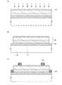
まず、半導体基板として、単結晶半導体基板100を準備する(図1(A−1)参照)。単結晶半導体基板100は、単結晶半導体基板や多結晶半導体基板を用いることができ、例えば、単結晶又は多結晶のシリコン基板や、ゲルマニウム基板、ガリウムヒ素やインジウムリン等の化合物半導体基板が挙げられる。市販のシリコン基板としては、直径5インチ(125mm)、直径6インチ(150mm)、直径8インチ(200mm)、直径12インチ(300mm)、直径16インチ(400mm)サイズの円形のものが代表的である。なお、形状は円形に限られず矩形状等に加工したシリコン基板を用いることも可能である。以下の説明では、単結晶半導体基板100として、単結晶シリコン基板を用いる場合について示す。
First, a single
また、単結晶半導体基板100の表面をあらかじめ硫酸過水(SPM)、アンモニア過水(APM)、塩酸過水(HPM)、希フッ酸(DHF)などを用いて適宜洗浄することが汚染除去の点から好ましい。また、希フッ酸とオゾン水を交互に吐出して洗浄してもよい。
In addition, the surface of the single
次に、単結晶半導体基板100上に絶縁膜102を形成する。絶縁膜102は、後に行うイオン照射工程において単結晶半導体基板の表面が荒れてしまうことを抑制するために形成する。また、ベース基板110に設けられる単結晶半導体層112の膜厚の均一性は、単結晶半導体基板100に形成される脆化領域104の深さの均一性に依存する。そして、脆化領域104の深さの均一性は、絶縁膜102の膜厚、膜質に依存する。したがって、絶縁膜102は、膜厚、膜質の均一性が高い膜であることが好ましい。また、ベース基板110に設けられる単結晶半導体層112の膜厚を厚くするためには、絶縁膜102の膜厚を薄くすることが好ましい。
Next, the insulating
膜厚、膜質の均一性の高い絶縁膜を形成するために、単結晶半導体基板100にラジカル処理により、絶縁膜102(第1の絶縁膜とも記す)を形成する(図1(A−2)参照)。本明細書において、ラジカル処理とは、プラズマを基板から離れた位置で生成し、活性化した原子又は分子のうち、長寿の中性原子又は中性分子を移送し、被処理物と反応させることをいう。また、ラジカルとは、電子が安定している通常(基底)状態に対して電子励起状態にある原子又は分子をいう。
In order to form an insulating film with high uniformity in film thickness and film quality, an insulating film 102 (also referred to as a first insulating film) is formed on the single
絶縁膜102は、酸化シリコン膜、窒化シリコン膜、酸化窒化シリコン膜、窒化酸化シリコン膜を用いることができる。絶縁膜102として酸化シリコン膜を形成する方法には、酸素を組成に含むガス(例えば、酸素(O2)又は一酸化二窒素(N2O))を励起して酸素ラジカルを生成し、酸素ラジカルにより単結晶半導体基板100を酸化する方法(酸素ラジカル処理ともいう)がある。また、窒化シリコン膜を形成する方法には、窒素を組成に含むガス(例えば、窒素ガス又はアンモニアガス等)を励起して窒素ラジカル又は窒化水素ラジカルを生成し、窒素ラジカル又は窒化水素ラジカルにより単結晶半導体基板100を窒化する方法(窒素ラジカル処理ともいう)がある。なお、本明細書においては、酸素ラジカル処理及び窒素ラジカル処理を含めてラジカル処理と呼ぶ。
As the insulating
絶縁膜102として酸化窒化シリコン膜を形成する方法には、酸素ラジカルによる酸化処理により単結晶半導体基板100の表面を酸化して酸化シリコン膜を形成し、この酸化シリコン膜を窒素ラジカルによる窒化処理により表面を窒化することで形成する方法がある。また、窒化酸化シリコン膜を形成する方法には、窒化ラジカルによる窒化処理により表面を窒化して窒化シリコン膜を形成し、この窒化シリコン膜を酸素ラジカルによる酸化処理により表面を酸化することで形成する方法がある。
In the method for forming a silicon oxynitride film as the insulating
酸素ラジカルによる酸化処理、若しくは窒素ラジカル又は窒化水素ラジカルによる窒化処理を行う場合には、マイクロ波でガスを励起してプラズマを生成することが好ましい。これは、電子密度が1×1011cm−3以上、且つ電子温度が3eV以下の高密度プラズマを生成することができるからである。高密度プラズマを生成するためのマイクロ波の代表的な周波数は2.45GHzである。高密度プラズマを用いることで、550℃以下の加熱温度で、実用的な反応速度で絶縁膜を形成することができる。つまり、マイクロ波によって高密度プラズマを生成させ、高密度プラズマで生成されたラジカルと処理物を反応させることで、基板加熱温度が550℃以下の低温且つ短時間で、処理物を固相反応によって酸化又は窒化をすることができる。 In the case of performing oxidation treatment with oxygen radicals or nitridation treatment with nitrogen radicals or hydrogen nitride radicals, it is preferable to generate plasma by exciting a gas with a microwave. This is because high density plasma having an electron density of 1 × 10 11 cm −3 or more and an electron temperature of 3 eV or less can be generated. A typical frequency of the microwave for generating the high density plasma is 2.45 GHz. By using high-density plasma, an insulating film can be formed at a practical reaction rate at a heating temperature of 550 ° C. or lower. In other words, by generating high-density plasma using microwaves and reacting radicals generated by the high-density plasma with the processed material, the processed material can be reacted by solid-phase reaction at a low temperature of 550 ° C. or less in a short time. It can be oxidized or nitrided.
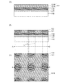
図2に、マイクロ波励起による高密度プラズマで各種の処理を行うための高密度プラズマ処理装置の構成例を示す。高密度プラズマを用いた処理には、半導体材料、絶縁材料、及び導電性材料に対する酸化処理、窒化処理、酸窒化処理、窒酸化処理、水素化処理、表面改質処理などがある。プラズマ励起するガスを変えることで、目的とする処理を行うことができる。 FIG. 2 shows a configuration example of a high-density plasma processing apparatus for performing various types of processing with high-density plasma by microwave excitation. Examples of the treatment using high-density plasma include oxidation treatment, nitridation treatment, oxynitridation treatment, nitrogen oxidation treatment, hydrogenation treatment, and surface modification treatment for semiconductor materials, insulating materials, and conductive materials. The target treatment can be performed by changing the plasma-excited gas.
図2(A)に示す高密度プラズマ処理装置は、マルチチャンバー構造であり、少なくとも第1のプラズマ処理室201、第2のプラズマ処理室202、ロードロック室203、及び共通室204を備えている。第1のプラズマ処理室201はラジカル酸化を行うためのチャンバーで、第2のプラズマ処理室202はラジカル窒化を行うためのチャンバーである。図2(A)に示す各チャンバーは、それぞれ真空排気されるようになっており、ラジカル酸化及びラジカル窒化を、単結晶半導体基板100を大気にさらすことなく連続的に行うことができる。
A high-density plasma processing apparatus illustrated in FIG. 2A has a multi-chamber structure, and includes at least a first
高密度プラズマ処理装置は、図2(A)に示す以外に、CVD用のチャンバー、スパッタ用のチャンバー、ドライエッチング用のチャンバー、イオンドーピング用のチャンバー、熱処理用のチャンバーなど、ラジカル酸化及びラジカル窒化以外の処理を行うことができるチャンバーをさらに備えていてもよい。 In addition to the high-density plasma processing apparatus shown in FIG. 2A, radical oxidation and radical nitridation such as a chamber for CVD, a chamber for sputtering, a chamber for dry etching, a chamber for ion doping, a chamber for heat treatment, etc. You may further provide the chamber which can perform processes other than these.
図2(B)は、第1のプラズマ処理室201及び第2のプラズマ処理室202に共通する構成を示す。プラズマ処理室200には、単結晶半導体基板100を配置するためのステージ211、ガス供給部212に連結されたシャワープレート218、プラズマ処理室200を排気するための真空ポンプに接続する排気口210を有する。プラズマ処理室200の上部には、アンテナ214、誘電体板216、マイクロ波発生部213に連結された同軸導波管215を有する。また、ステージ211に温度制御部219を設けることによって単結晶半導体基板100の温度を制御することも可能である。
FIG. 2B illustrates a structure common to the first
ラジカル処理を行うには、所定のガスをガス供給部212から供給する。ガスはシャワープレート218の孔を通って、プラズマ処理室200に導入される。マイクロ波発生部213から、周波数2.45GHzのマイクロ波を発生させ、同軸導波管215へ供給する。マイクロ波は同軸導波管215、アンテナ214から誘電体板216を通してプラズマ処理室200に供給される。マイクロ波によって、プラズマ処理室200に供給されたガスが励起され、高密度プラズマが生成される。ステージ211とシャワープレート218との間隔(以下、電極間隔ともいう)は、20mm以上80mm以下とすることができ、この間隔は、20mm以上60mm以下が好ましい。また、温度制御部219によって、単結晶半導体基板100を加熱しながらラジカル処理することができる。
In order to perform the radical treatment, a predetermined gas is supplied from the
酸素ラジカル処理を行う場合には、プラズマ励起させるガスに、酸素を組成に含むガスと共に、希ガスを含ませることが好ましい。なお、酸素を組成に含むガスは、例えば、酸素(O2)、一酸化二窒素(N2O)などである。また、窒素ラジカル処理を行う場合も、プラズマ励起させるガスに、窒素を組成に含むガスと共に希ガスを含ませることが好ましい。なお、窒素を組成に含むガスは、例えば、窒素(N2)、アンモニア(NH3)などである。希ガスを添加することで、プラズマ中に効率良く酸素ラジカル(以下、「O*」と表記する。)、窒素ラジカル(以下、「N*」と表記する。)を生成することができる。希ガスとして、He、Ne、Ar、Kr、およびXeから選ばれる1種類又は複数種類のガスをも用いることができる。高密度プラズマを生成するためには、原子半径がより大きい、Ar、Kr、及びXeが好ましい。 In the case of performing oxygen radical treatment, it is preferable that a gas to be plasma-excited contains a rare gas together with a gas containing oxygen in the composition. Note that the gas containing oxygen in the composition is, for example, oxygen (O 2 ), dinitrogen monoxide (N 2 O), or the like. In addition, also in the case of performing nitrogen radical treatment, it is preferable to include a rare gas together with a gas containing nitrogen in the gas to be excited by plasma. The gas containing nitrogen in the composition is, for example, nitrogen (N 2 ), ammonia (NH 3 ), or the like. By adding a rare gas, oxygen radicals (hereinafter referred to as “O * ”) and nitrogen radicals (hereinafter referred to as “N * ”) can be efficiently generated in the plasma. As the rare gas, one or more kinds of gases selected from He, Ne, Ar, Kr, and Xe can also be used. In order to generate a high-density plasma, Ar, Kr, and Xe having a larger atomic radius are preferable.
図2の高密度プラズマ処理装置を用いて、単結晶半導体基板100を酸素ラジカル処理する方法の一例を説明する。ガス供給部212からO2、Krをそれぞれプラズマ処理室200に供給する。そして、マイクロ波をプラズマ処理室200に導入することで、O2およびKrの混合ガスのプラズマが生成される。このプラズマ中では、導入されたマイクロ波によりKrが励起されて、Krラジカル(以下、「Kr*」と表記する。)が生成され、このKr*と酸素分子(O2)とが衝突することにより、O*が生成される。そして、プラズマ中で生成されたO*とステージ211上の単結晶半導体基板100が反応して、単結晶半導体基板100が酸化される。また、さらに、酸素を組成に含むガス、希ガス共に水素(H2)ガスを励起することで、プラズマ中にOHラジカル(以下、「OH*」と表記する)を生成させて、OH*により単結晶半導体基板100を酸化することもできる。酸素ラジカル処理のための加熱温度は、300℃以上550℃以下の範囲とすることができる。圧力は100Pa以上140Pa以下が好ましい。
An example of a method for oxygen radical treatment of the single
図2の高密度プラズマ処理装置を用いて、単結晶半導体基板100を窒素ラジカル処理する方法の一例を説明する。ガス供給部212からN2、Krをそれぞれプラズマ処理室200に供給する。そして、マイクロ波をプラズマ処理室200に導入することで、N2およびKrの混合ガスのプラズマが生成される。このプラズマ中では、導入されたマイクロ波によりKrが励起されて、Kr*が生成され、このKr*と窒素分子(N2)とが衝突することにより、N*が生成される。そして、プラズマ中で生成されたN*とステージ211上の単結晶半導体基板100が反応して、単結晶半導体基板100が窒化される。また、N2、H2および希ガスの混合ガス、またはNH3と希ガスの混合ガスを励起することで、窒素ラジカル処理を行うことができる。これらの混合ガスのプラズマ中には、N*およびNHラジカル(以下、「NH*」と表記する)が生成され、N*、NH*により単結晶半導体基板100が窒化される。窒素ラジカル処理のための加熱温度は、300℃以上550℃以下の範囲とすることができる。圧力は5Pa以上15Pa以下が好ましい。
An example of a method for nitrogen radical treatment of the single
ラジカル処理による第1絶縁膜102の形成方法の一例を説明する。まず、高密度プラズマによりO*を生成し、単結晶半導体基板100の表面を酸化して1nm〜10nmの厚さの酸化シリコン膜を形成する。さらに、高密度プラズマにより窒素ラジカルを生成し、窒素ラジカルにより酸化シリコン膜の上部を窒化してもよい。酸化シリコン膜に窒化を行うことで、酸化窒化シリコン膜を形成することができる。または、高密度プラズマにより窒化ラジカルを生成し、単結晶半導体基板100の表面を窒化して、1nm〜10nmの厚さの窒化シリコン膜を形成する。さらに、高密度プラズマにより酸素ラジカルを生成し、酸素ラジカルにより窒化シリコン膜の上部を酸化してもよい。窒化シリコン膜に酸化を行うことで、窒化酸化シリコン膜を形成することができる。
An example of a method for forming the first insulating
ラジカル処理は、基板へのダメージが少なく反応性の高い中性原子又は中性分子がシリコン界面を原子レベルで平坦化すると共に、シリコン界面に存在するダングリングボンドを終端することで、界面準位密度や固定電荷の少ない高品質な絶縁膜を形成することができる。よって、ラジカル処理により、膜厚、膜質の均一性が高い絶縁膜を形成することができる。また、ラジカル処理による単結晶半導体基板100の酸化又は窒化は、原子レベルで制御ができるため、極薄(数nm程度)の膜厚の絶縁膜102を形成することができる。
In radical treatment, neutral atoms or neutral molecules that are highly reactive and have little damage to the substrate planarize the silicon interface at the atomic level, and terminate dangling bonds that exist at the silicon interface. A high-quality insulating film with low density and fixed charge can be formed. Therefore, an insulating film with high uniformity in film thickness and film quality can be formed by radical treatment. In addition, since oxidation or nitridation of the single
次に、運動エネルギーを有するイオン103を単結晶半導体基板100に照射することで、単結晶半導体基板100の所定の深さに結晶構造が損傷された脆化領域104を形成する(図1(A−3)参照)。図1(A−3)に示すように、絶縁膜102を介して、加速されたイオン103を単結晶半導体基板100に照射することで、単結晶半導体基板100の表面から所定の深さの領域にイオン103が導入され、脆化領域104を形成することができる。イオン103は、ソースガスを励起して、ソースガスのプラズマを生成し、このプラズマに含まれるイオンを、電界の作用によりプラズマから引き出して、加速したイオンである。
Next, the single
脆化領域104が形成される領域の深さは、イオン103の運動エネルギー、質量、電荷、入射角によって調節することができる。また、運動エネルギーは加速電圧などにより調節できる。また、脆化領域104が形成される深さは、絶縁膜102の膜厚によっても調節することができる。脆化領域104は、イオン103の平均侵入深さとほぼ同じ深さの領域に形成される。そのため、イオン103を添加する深さで、単結晶半導体基板100から分離される半導体層の厚さが決定される。この半導体層の厚さが110nm以上500nm以下、好ましくは200nm以上350nm以下になるように、脆化領域104が形成される深さを調節する。例えば、半導体層の厚さを300nmとする場合、イオンの深さ方向プロファイルのピーク値が300nmとなるようにイオンを照射すればよい。
The depth of the region where the embrittled
脆化領域104の形成は、イオンドーピング処理で行うことができる。イオンドーピング処理には、イオンドーピング装置を用いて行うことができる。イオンドーピング装置の代表的な装置は、プロセスガスをプラズマ励起して生成された全てのイオン種をチャンバー内に配置された被処理体に照射する非質量分離型の装置である。非質量分離型の装置であるのは、プラズマ中のイオン種を質量分離しないで、全てのイオン種を被処理体に照射しているからである。これに対して、イオン注入装置は質量分離型の装置である。イオン注入装置は、プラズマ中のイオン種を質量分離し、ある特定の質量のイオン種を被処理体に照射する装置である。
The
イオンドーピング装置の主要な構成は、被処理物を配置するチャンバー、所望のイオンを発生させるイオン源、およびイオンを加速し、照射するための加速機構である。イオン源は、所望のイオン種を生成するためのソースガスを供給するガス供給装置、ソースガスを励起して、プラズマを生成させるための電極などで構成される。プラズマを形成するための電極として、フィラメント型の電極や容量結合高周波放電用の電極などが用いられる。加速機構は、引出電極、加速電極、減速電極、接地電極等の電極など、およびこれらの電極に電力を供給するための電源などで構成される。加速機構を構成する電極には複数の開口やスリットが設けられており、イオン源で生成されたイオンは電極に設けられた開口やスリットを通過して加速される。なお、イオンドーピング装置の構成は上述したものに限定されず、必要に応じた機構が設けられる。 The main components of the ion doping apparatus are a chamber in which an object to be processed is arranged, an ion source for generating desired ions, and an acceleration mechanism for accelerating and irradiating ions. The ion source includes a gas supply device that supplies a source gas for generating a desired ion species, an electrode for generating a plasma by exciting the source gas, and the like. As an electrode for forming plasma, a filament-type electrode, an electrode for capacitively coupled high-frequency discharge, or the like is used. The acceleration mechanism includes an electrode such as an extraction electrode, an acceleration electrode, a deceleration electrode, and a ground electrode, and a power source for supplying power to these electrodes. The electrode constituting the acceleration mechanism is provided with a plurality of openings and slits, and ions generated by the ion source are accelerated through the openings and slits provided in the electrodes. Note that the configuration of the ion doping apparatus is not limited to that described above, and a mechanism according to need is provided.
本実施形態では、イオンドーピング装置で、イオンを単結晶半導体基板100に照射する。プラズマソースガスとして水素を含むガスを供給する。例えば、H2を供給する。水素ガスを励起してプラズマを生成し、質量分離せずに、プラズマ中に含まれるイオンを加速し、加速されたイオンを単結晶半導体基板100に照射する。
In this embodiment, the single
イオンドーピング装置において、水素ガスから生成されるイオン種(H+、H2 +、H3 +)の総量に対してH3 +の割合が50%以上とする。より好ましくは、H3 +の割合を80%以上とする。イオンドーピング装置は質量分離を行わないため、プラズマ中に生成される複数のイオン種のうち、1つ(H3 +)を50%以上とすることが好ましく、80%以上とすることがより好ましい。同じ質量のイオンを照射することで、単結晶半導体基板100の同じ深さに集中させてイオンを添加することができる。ここで、複数のイオン種のうち同じ質量のイオンが50%以上含まれるとき、当該イオンを主成分という。上記において、H3 +を主成分とする複数のイオンを単結晶半導体基板100に照射する。
In the ion doping apparatus, the ratio of H 3 + to the total amount of ion species (H + , H 2 + , H 3 + ) generated from hydrogen gas is 50% or more. More preferably, the ratio of H 3 + is 80% or more. Since the ion doping apparatus does not perform mass separation, it is preferable that one (H 3 + ) of the plurality of ion species generated in the plasma is 50% or more, and more preferably 80% or more. . By irradiation with ions having the same mass, ions can be added while being concentrated at the same depth in the single
イオンドーピング装置は廉価で、大面積処理に優れているため、このようなイオンドーピング装置を用いてH3 +を照射することで、半導体特性の向上、大面積化、低コスト化、生産性向上などの顕著な効果を得ることができる。また、イオンドーピング装置を用いた場合、重金属も同時に導入されるおそれがあるが、ラジカル処理により形成された絶縁膜102を介してイオンの照射を行うことによって、これらの重金属による単結晶半導体基板100の汚染を低減することができる。
Since the ion doping apparatus is inexpensive and excellent in large area processing, irradiation with H 3 + using such an ion doping apparatus improves the semiconductor characteristics, increases the area, reduces the cost, and improves the productivity. A remarkable effect such as can be obtained. Further, when an ion doping apparatus is used, heavy metals may be introduced at the same time. However, by irradiating ions through the insulating
なお、加速されたイオン103を単結晶半導体基板100に照射する工程は、イオン注入装置で行うこともできる。イオン注入装置は、チャンバー内に配置された被処理体に、ソースガスをプラズマ励起して生成された複数のイオン種を質量分離し、特定のイオン種を照射する質量分離型の装置である。したがって、イオン注入装置を用いる場合は、水素ガスやPH3を励起して生成されたH+イオンおよびH2 +イオンを質量分離して、H+イオンまたはH2 +イオンの一方のイオンを加速して、単結晶半導体基板100に照射する。
Note that the step of irradiating the single
ラジカル処理により形成された絶縁膜102は、膜厚及び膜質の均一性が高く、緻密性が高い。また、原子レベルでの制御ができるため、極薄(数nm程度)の膜厚を形成することができる。ラジカル処理により形成された絶縁膜102を用いることによって、絶縁膜102を介して単結晶半導体基板100に照射されるイオンを、均一に添加することができる。絶縁膜102の膜質の緻密性が高いため、イオンの照射による表面荒れを低減することができる。絶縁膜102の膜厚は、数nm程度の膜厚なので、絶縁膜102を数十nmで設けた場合よりも、深く添加することができる。よって、ラジカル処理により、絶縁膜102を形成してイオンの照射を行うことによって、単結晶半導体基板100の深い領域に均一な脆化領域を形成することができる。したがって、単結晶半導体層の膜厚均一性が高いSOI基板を作製することができる。
The insulating
次に、絶縁膜102上に、絶縁膜105(第2の絶縁膜とも記す)を形成する(図1(A−4)参照)。 Next, an insulating film 105 (also referred to as a second insulating film) is formed over the insulating film 102 (see FIG. 1A-4).
絶縁膜105は、単層構造又は2層以上の積層構造とすることができる。絶縁膜105を構成する膜には、酸化シリコン膜、窒化シリコン膜、酸化窒化シリコン膜、窒化酸化シリコン膜、酸化ゲルマニウム膜、窒化ゲルマニウム膜、酸化窒化ゲルマニウム膜、窒化酸化ゲルマニウム膜などのシリコン又はゲルマニウムを組成に含む膜を用いることができる。また、酸化アルミニウム、酸化タンタル、酸化ハフニウムなどの金属の酸化物でなる絶縁膜、窒化アルミニウムなどの金属の窒化物でなる絶縁膜、酸化窒化アルミニウム膜などの金属の酸化窒化物でなる絶縁膜、窒化酸化アルミニウム膜などの金属の窒化酸化物でなる絶縁膜を用いることもできる。
The insulating
絶縁膜105は、化学気相法(CVD;Chemical Vapor Deposition)、スパッタリング法、原子エピタキシ(ALE)法により形成することができる。CVD法は、減圧CVD法、熱CVD法、プラズマ励起CVD法(以下、PECVD法という)などがある。PECVD法は、350℃以下の低温処理であり、また他のCVD法よりも成膜速度が速いので好ましい。
The insulating
本実施の形態では、絶縁膜105を絶縁膜105a、105bの2層構造で形成する例を示す。絶縁膜102が除去された単結晶半導体基板100上に、絶縁膜105aと、絶縁膜105bを積層する。絶縁膜105aは、化学的な反応により形成される絶縁膜が好ましく、特に酸化シリコンが好ましい。絶縁膜105aとして、酸化シリコンをCVD法で形成する場合には、シリコンのソースガスとして有機シランガスを用いることが好ましい。酸素のソースガスには酸素気体を用いることができる。有機シランガスには、酸化エチル(TEOS:化学式Si(OC2H5)4)、トリメチルシラン(TMS:(CH3)3SiH)、テトラメチルシラン(TMS:化学式Si(CH3)4)、テトラメチルシクロテトラシロキサン(TMCTS)、オクタメチルシクロテトラシロキサン(OMCTS)、ヘキサメチルジシラザン(HMDS)、トリエトキシシラン(SiH(OC2H5)3)、又はトリスジメチルアミノシラン(SiH(N(CH3)2)3)などを用いることができる。
In this embodiment, an example in which the insulating
絶縁膜105aとなる酸化シリコン膜は、熱CVD法で、加熱温度が500℃以下200℃以上で形成されるLTO(低温酸化物、Low Temperature Oxide)で形成することができる。この場合、シリコンのソースガスにシラン(SiH4)又はジシラン(Si2H6)等を用い、酸素ソースガスに酸素(O2)又は一酸化二窒素(N2O)等を用いることができる。また、単結晶半導体基板100に脆化領域104が形成された後に、絶縁膜105aを形成する場合には、絶縁膜105aは300℃以下好ましくは200℃以下で形成されることが好ましい。単結晶半導体基板100に添加された水素が脱離してしまうのを防ぐためである。膜厚は、10nm以上200nm以下、好ましくは、50nm以上100nm以下の範囲で設けることが好ましい。
The silicon oxide film to be the insulating
絶縁膜105bは、窒化シリコン膜(SiNx)又は窒化酸化シリコン膜((SiNxOy)(x>y))等の窒素を含有する膜(窒素含有層とも記す)で形成する。本実施の形態において、絶縁膜105bは、ベース基板110と貼り合わされる層(接合層)となる。また、絶縁膜105bは、後にベース基板上に単結晶構造を有する半導体層(以下、単結晶半導体層と記す)を設けた際に、ベース基板に含まれるナトリウム(Na)等の不純物が単結晶半導体層に拡散することを防ぐためのバリア層として機能する。
The insulating
また、絶縁膜105bは接合層として用いるため、接合不良を抑制するには絶縁膜105bの表面を平滑とすることが好ましい。具体的には、絶縁膜105bの平均面粗さ(Ra)を0.5nm以下、自乗平均粗さ(Rms)を0.60nm以下、より好ましくは、平均面粗さを0.35nm以下、自乗平均粗さを0.45nm以下となるように絶縁膜105bを形成する。膜厚は、10nm以上200nm以下、好ましくは、50nm以上100nm以下の範囲で設けることが好ましい。なお、貼り合わせに係る接合層は、ベース基板側に設けた場合においても、上記の範囲の平均面粗さ、自乗平均粗さで設けることが好ましい。
In addition, since the insulating
また、ベース基板110との接合には、水素結合が大きく寄与するため、絶縁膜105bに水素が含まれるように成膜することが好ましい。絶縁膜105bとして、水素を含有する窒化シリコン膜又は窒化酸化シリコン膜を用いることによって、Si−OH、N−OHを結合手として、ガラス等のベース基板110と水素結合によって強固に接合することができる。
Further, since hydrogen bonding greatly contributes to bonding with the
このような絶縁膜105bを形成するため、本実施の形態では、プラズマCVD法を用いて、成膜時の基板温度を室温以上350℃以下、好ましくは、室温以上300℃以下として窒化シリコン膜又は窒化酸化シリコン膜の成膜を行うことが好ましい。成膜時の基板温度を低くすることによって、形成される絶縁膜105bの表面粗さを小さくすることができる。これは、成膜時の基板温度が高くなるにつれて膜の堆積表面でのラジカル等によるエッチング反応が過多となり表面荒れを起こすためである。また、単結晶半導体基板100に添加された水素が脱離してしまうのを防ぐことができる。
In this embodiment, in order to form such an
また、本実施の形態では、プラズマCVD法において、少なくともシランガス、アンモニアガス及び水素ガスを用いて成膜を行うことが好ましい。アンモニアガスや水素ガスを用いることによって、膜中に水素を含む絶縁膜105bを形成することができる。また、成膜時の基板温度を低くすることによって、成膜中の脱水素反応が抑制され、絶縁膜105bに含まれる水素の量を多くすることができるという利点もある。
In this embodiment, it is preferable to perform film formation using at least silane gas, ammonia gas, and hydrogen gas in a plasma CVD method. By using ammonia gas or hydrogen gas, the insulating
また、プラズマCVD法において、成膜時の基板温度を低くすることにより得られた絶縁膜105bは、水素を多く含んでおり緻密性が低い膜となる。緻密性が低い絶縁膜105bは、加熱処理により緻密性を高めることができるため、加熱処理の前後で膜厚が収縮しうる。そのため、絶縁膜105bの緻密性が低い状態でベース基板との貼り合わせを行うことによって、ベース基板の表面や絶縁膜105bの表面に凹凸がある場合であっても、当該絶縁膜105bの収縮により凹凸を吸収することができ、接合不良を低減することが可能となる。また、貼り合わせと同時又はその後に加熱処理を行うことによって、絶縁膜105bを緻密化した後に、トランジスタ等の素子を形成することができる。
In the plasma CVD method, the insulating
ラジカル処理により形成された絶縁膜102を用いて、単結晶半導体基板100にイオンの照射を行うことで、絶縁膜102の表面荒れを低減することができる。したがって、絶縁膜102上に、さらに絶縁膜105を堆積しても絶縁膜105の表面の凹凸に影響を及ぼさないため、絶縁膜105を平坦に形成することができる。
By irradiating the single
次に、ベース基板110を準備する(図1(B)参照)。ベース基板110は、絶縁体でなる基板を用いる。具体的には、アルミノシリケートガラス、アルミノホウケイ酸ガラス、バリウムホウケイ酸ガラスのような電子工業用に使われる各種ガラス基板、石英基板、セラミック基板、サファイア基板が挙げられる。本実施の形態では、ガラス基板を用いる場合について説明する。ベース基板110として大面積化が可能で安価なガラス基板を用いることにより、シリコンウエハを用いる場合と比較して低コスト化を図ることができる。
Next, the
次に、単結晶半導体基板100とベース基板110とを対向させ、絶縁膜105bの表面とベース基板110の表面とを接合させる(図1(C)参照)。
Next, the single
ここでは、単結晶半導体基板100とベース基板110とを、絶縁膜105を介して密着させた後、単結晶半導体基板100の一箇所に1〜500N/cm2、好ましくは1〜20N/cm2程度の圧力を加える。圧力を加えた部分から絶縁膜105とベース基板110が接合しはじめ、自発的に接合が形成されほぼ全面におよぶ。この接合工程は、ファンデルワールス力や水素結合が作用しており、加熱処理を伴わず、常温で行うことができるため、ベース基板110に、ガラス基板のように耐熱温度が低い基板を用いることができる。また、絶縁膜105は平坦に形成されているため、貼り合わせ面内での局所的な隙間(ボイド)が生じにくく、貼り合わせ強度を高めることができる。
Here, after the single
なお、単結晶半導体基板100とベース基板110との貼り合わせを行う前に、単結晶半導体基板100上に形成された絶縁膜105と、ベース基板110の少なくとも一方に表面処理を行うことが好ましい。
Note that before the single
表面処理としては、プラズマ処理、オゾン処理、メガソニック洗浄、2流体洗浄(純水や水素添加水等の機能水を窒素等のキャリアガスとともに吹き付ける方法)又はこれらの方法を組み合わせて行うことができる。特に、絶縁膜105とベース基板110の少なくとも一方の表面にプラズマ処理を行った後に、単結晶半導体基板100及びベース基板110にオゾン処理、メガソニック洗浄、2流体洗浄等を行うことによって、被処理面の有機物等のゴミを除去し、表面を親水化することができる。その結果、絶縁膜105とベース基板110接合強度を向上させることができる。ここでのプラズマ処理は、不活性ガス(例えば、アルゴン(Ar)ガス)及び/又は反応性ガス(例えば、酸素(O2)ガス、窒素(N2)ガス)を用いて、RIE法、ICP法、大気圧プラズマを行う。
As the surface treatment, plasma treatment, ozone treatment, megasonic cleaning, two-fluid cleaning (a method of spraying functional water such as pure water or hydrogenated water together with a carrier gas such as nitrogen) or a combination of these methods can be performed. . In particular, after plasma treatment is performed on at least one surface of the insulating
また、ベース基板110に単結晶半導体基板100を接合させた後、絶縁膜105とベース基板110との接合強度を増加させるための熱処理を行うことが好ましい。この熱処理の温度は、脆化領域104に亀裂を発生させない温度とし、例えば、室温以上400℃未満の温度範囲で処理する。また、この温度範囲で加熱しながら、絶縁膜105とベース基板110とを接合させてもよい。熱処理には、拡散炉、抵抗加熱炉などの加熱炉、RTA(瞬間熱アニール、Rapid Thermal Anneal)装置、マイクロ波加熱装置などを用いることができる。
In addition, after the single
一般的に、絶縁膜105とベース基板110を接合と同時又は接合させた後に熱処理を行うと、接合界面において脱水反応が進行し、接合界面同士が近づき、水素結合の強化や共有結合が形成されることにより接合が強化される。脱水反応を促進させるためには、脱水反応により接合界面に生じる水分を高温で熱処理を行うことにより除去する必要がある。つまり、接合後の熱処理温度が低い場合には、脱水反応で接合界面に生じた水分を効果的に除去できないため、脱水反応が進まず接合強度を十分に向上させることが難しい。
In general, when heat treatment is performed at the same time as or after bonding the insulating
本実施の形態では、ベース基板110としてガラス等の耐熱性が低い基板を用いた場合であっても、絶縁膜105とベース基板110の接合強度を十分に向上させることが可能となる。また、貼り合わせの前にバイアス電圧を印加してプラズマ処理を行った場合は、低温であっても絶縁膜105とベース基板110の接合強度を向上させることができる。
In this embodiment, even when a substrate with low heat resistance such as glass is used as the
次に、熱処理を行い脆化領域104において分離(劈開)することにより、ベース基板110上に、絶縁膜102、105を介して単結晶半導体層112(以下、第1の単結晶半導体層112と記す)を設けることができる(図1(D)参照)。
Next, heat treatment is performed and separation (cleavage) is performed in the
加熱処理を行うことで、温度上昇によって脆化領域104に形成されている微小な孔内部の圧力が上昇する。圧力の上昇により脆化領域104の微小な孔に体積変化が起こり、脆化領域104に亀裂が生じるので、脆化領域104に沿って単結晶半導体基板100が劈開(分離)する。絶縁膜105はベース基板110に接合しているので、ベース基板110上には単結晶半導体基板100から分離された第1の単結晶半導体層112が形成される。また、ここでの熱処理の温度は、ベース基板110の歪点を超えない温度とする。
By performing the heat treatment, the pressure inside the minute hole formed in the embrittled
この加熱処理には、拡散炉、抵抗加熱炉などの加熱炉、RTA(瞬間熱アニール、Rapid Thermal Anneal)装置、マイクロ波加熱装置などを用いることができる。例えば、RTA装置を用いる場合、加熱温度550℃以上730℃以下、処理時間0.5分以上60分以内で行うことができる。 For this heat treatment, a heating furnace such as a diffusion furnace or a resistance heating furnace, a rapid thermal annealing (RTA) apparatus, a microwave heating apparatus, or the like can be used. For example, when an RTA apparatus is used, the heating temperature can be 550 ° C. or higher and 730 ° C. or lower, and the treatment time can be 0.5 minutes or longer and 60 minutes or less.
なお、上述したベース基板110と絶縁膜105との接合強度を増加させるための熱処理を行わず、絶縁膜105とベース基板110との接合強度の増加の熱処理工程と、脆化領域104における分離の熱処理工程を同時に行ってもよい。
Note that the above heat treatment for increasing the bonding strength between the
以上の工程により、ベース基板110上に絶縁膜102、絶縁膜105を介して第1の単結晶半導体層112が設けることができる(図1(D)参照)。
Through the above steps, the first single
一般的に、分離後におけるベース基板110上に形成された第1の単結晶半導体層112は、脆化領域104の形成及び脆化領域104における分離により、結晶欠陥等が形成され、平坦性が劣化した状態となっている(図1(D)参照)。また、第1の単結晶半導体層112の表面に、自然酸化膜が形成される場合もある。そこで、第1の単結晶半導体層112の欠陥修復処理又は表面平坦化処理を行っても良い。なお、以下に示す欠陥修復処理又は表面平坦化処理は必須の工程ではない。
In general, in the first single
欠陥修復処理又は表面平坦化処理は、エッチング処理又はレーザビームの照射の一方又は双方を組み合わせて行う。エッチング処理としては、ドライエッチング、ウェットエッチング、又は両者を組み合わせて行う。また、エッチング処理の代わりにCMP等の研磨処理を行ってもよい。 The defect repairing process or the surface flattening process is performed by combining one or both of etching process and laser beam irradiation. As the etching process, dry etching, wet etching, or a combination of both is performed. Further, a polishing process such as CMP may be performed instead of the etching process.
エッチング処理は、例えば、反応性イオンエッチング(RIE:Reactive Ion Etching)法、ICP(Inductively Coupled Plasma)エッチング法、ECR(Electron Cyclotron Resonance)エッチング法、平行平板型(容量結合型)エッチング法、マグネトロンプラズマエッチング法、2周波プラズマエッチング法またはヘリコン波プラズマエッチング法等を用いることができる。エッチングガスは、例えば、Cl2、BCl3、SiCl4等の塩素系のガス、CHF3、CF4、C4F8、C2F6、NF3、弗化硫黄等のフッ素系のガス、HBr等の臭素系のガスを用いることによりエッチングすることが可能である。その他、HeやArやXeなどの不活性ガス、又はO2ガス、H2ガスを用いることができる。なお、エッチング処理は、複数回に分けて行ってもよい。第1の単結晶半導体層112に存在する欠陥の大きさや深さは、イオンを添加するエネルギーの大きさやドーズ量に起因するため、エッチング処理によって第1の単結晶半導体層112の表面を除去する膜厚は、エッチング処理前の第1の単結晶半導体層112の膜厚とその表面粗さの程度によって適宜設定すればよい。例えば、エッチング処理により、第1の単結晶半導体層112を1nm以上30nm以下除去することが好ましい。エッチング処理を行うことにより、第1の単結晶半導体層112表面に形成された欠陥の除去を行うことができ、第1の単結晶半導体層112の表面荒れを低減することができる。
Etching processes include, for example, reactive ion etching (RIE) method, ICP (Inductively Coupled Plasma) etching method, ECR (Electron Cyclotron Resonance) etching method, parallel plate type (capacitive coupling type) etching method, magnetron plasma. An etching method, a two-frequency plasma etching method, a helicon wave plasma etching method, or the like can be used. Etching gas is, for example, chlorine gas such as Cl 2 , BCl 3 , SiCl 4 , fluorine gas such as CHF 3 , CF 4 , C 4 F 8 , C 2 F 6 , NF 3 , sulfur fluoride, Etching can be performed by using a bromine-based gas such as HBr. In addition, an inert gas such as He, Ar, or Xe, or O 2 gas or H 2 gas can be used. Note that the etching treatment may be performed in multiple steps. Since the size and depth of defects present in the first single
エッチング処理により、ベース基板110上に形成された第1の単結晶半導体層112の表層部を除去することにより、第1の単結晶半導体層112の結晶欠陥等の除去、平坦化を図ることができる。
By removing the surface layer portion of the first single
第1の単結晶半導体層112の内部には、脆化領域104形成のためのイオン照射工程によって結晶欠陥が形成されている。第1の単結晶半導体層112の分離面側から、または、ベース基板110側からレーザビームを照射することで、第1の単結晶半導体層112を溶融させ、結晶性の改善および平坦性の向上を図る。第1の単結晶半導体層112にレーザビームを照射することで、第1の単結晶半導体層112を部分溶融又は完全溶融させる。
A crystal defect is formed in the first single
好ましくは、レーザビームの照射により、第1の単結晶半導体層112を部分溶融させる。第1の単結晶半導体層112を部分溶融させることで、溶融されていない固相部分から結晶成長が進行するため、結晶性を低下させることなく、結晶欠陥を修復することができる。なお、本明細書において、部分溶融とは、単結晶半導体層の一部(例えば、上層部分)は溶融されて液相状態となるが、その他(例えば、下層部分)は溶融せずに固相状態のままであることをいう。また、完全溶融とは、単結晶半導体層が下部界面付近まで溶融されて、液相状態になることをいう。
Preferably, the first single
レーザビームの照射により部分溶融させながら、レーザビームを走査することで、溶融されていない固相部分から結晶成長が進行する。これにより、第1の単結晶半導体層112の結晶欠陥が減少し、結晶性が向上する。溶融されていない部分は、単結晶であり、結晶方位が揃っているため、結晶粒界が形成されず、レーザビーム照射後の第1の単結晶半導体層112は、結晶粒界のない単結晶半導体層とすることができる。また、溶融された領域は凝固することで再単結晶化するが、隣接している溶融していない部分の単結晶半導体と結晶方位が揃った単結晶半導体が形成される。よって、主表面の面方位が(100)の単結晶シリコンを単結晶半導体基板100として用いた場合、第1の単結晶半導体層112の主表面の面方位は(100)であり、レーザビーム照射によって溶融し、再単結晶化された第1の単結晶半導体層112の主表面の面方位(100)になる。なお、レーザビーム照射の代わりにRTAやフラッシュランプ照射を行ってもよい。
By scanning the laser beam while partially melting it by irradiation with the laser beam, crystal growth proceeds from a solid phase portion that is not melted. Accordingly, crystal defects in the first single
エッチング処理を行った後に、レーザビームを照射することで、単結晶半導体層に結晶欠陥や汚染物等が取り込まれてしまうことを防ぐことができる。また、自然酸化膜を除去することによって、レーザビームの照射による表面荒れを防ぐことができる。 Irradiation with a laser beam after the etching treatment can prevent crystal defects, contaminants, and the like from being taken into the single crystal semiconductor layer. Further, by removing the natural oxide film, surface roughness due to laser beam irradiation can be prevented.
以上により、単結晶半導体基板100から分離して形成された第1の単結晶半導体層112を有するSOI基板を作製することができる。なお、以下の工程は、上記の結晶修復処理又は表面平坦化処理を行った後に行っても良いし、結晶修復処理又は表面平坦化処理を行わずに行ってもよい。
Through the above steps, an SOI substrate including the first single
次に、第1の単結晶半導体層112上に第1の半導体層113Aを形成する(図3(B)参照)。例えば、気相成長(気相エピタキシャル成長)法を用いて形成する(図3(B)参照)。すなわち、第1の半導体層113Aは、第1の単結晶半導体層112の結晶性の影響を受けた半導体層である。ここで、第1の半導体層113Aは、第1の単結晶半導体層112に合わせて材料を選択し、形成すればよい。第1の半導体層113Aとしてシリコン層を形成する場合には、例えば、シラン系ガス(代表的にはシラン)と水素ガスとの混合ガスを原料として、プラズマCVD法により形成することができる。また、第1の半導体層113Aは、5nm以上100nm以下、好ましくは10nm以上50nm以下程度の厚さとなるように形成する。
Next, a
なお、第1の半導体層113Aのエピタキシャル成長を行う前に、第1の単結晶半導体層112表面に形成されている自然酸化膜などは除去しておくことが好ましい。これは、第1の単結晶半導体層112の表面に酸化層が存在する場合には、第1の単結晶半導体層112の結晶性を受けたエピタキシャル成長を進行させることができず、第1の半導体層113Aの結晶性が低下してしまうためである。ここで、上記の酸化層の除去は、フッ酸系の溶液などを用いて行うことができる。
Note that a natural oxide film or the like formed on the surface of the first single
次に、第1の半導体層113A上に第1の半導体層113Bを形成する(図3(C)参照)。ここで、第1の半導体層113Bは、第1の半導体層113Aに合わせて材料を選択し、形成する。また、第1の半導体層113Bは、200nm以上(好ましくは400nm以上)の厚さとなるように形成する。この場合においても、第1の半導体層113A表面に形成されている酸化層は除去しておくことが好ましい。
Next, the
第1の半導体層113Bは、第1の半導体層113Aと比較して結晶性が低い半導体層とする。または、第1の半導体層113Bは、第1の半導体層113Aと比較して水素濃度が高い半導体層(水素含有量が大きい半導体層)とする。このような第1の半導体層113Bとしては、例えば、非晶質半導体層を形成すればよい。
The
第1の半導体層113Bの形成方法は任意であるが、少なくとも第1の半導体層113Aより成膜速度が高い条件で形成することが好ましい。例えば、シラン系ガス(代表的にはシラン)と水素ガスとの混合ガスを原料として、プラズマCVD法により第1の半導体層113Bを形成する場合には、シラン系ガスに対する水素ガスの流量比を2倍以上20倍以下(好ましくは5倍以上15倍以下)とすればよい。また、周波数を10MHz乃至200MHz、電力を5W以上50W以下、チャンバー内圧力を10Pa以上103Pa以下、電極間隔(平行平板型の場合)を15mm以上30mm以下、ベース基板110の温度を200℃以上400℃以下とすると良い。代表的には、シラン(SiH4)の流量を25sccm、水素の流量を150sccm、周波数を27MHz、電力を30W、圧力を66.6Pa、電極間隔を25mm、基板温度を280℃とする。なお、上記の成膜条件は一例に過ぎず、本発明はこれに限定して解釈されるものではない。ここで重要な点は、第1の半導体層113Bとして結晶性は低くとも(又は水素濃度が高くとも)成膜速度の高い半導体層を形成することであるから、この目的を達成することができれば、どのような形成方法で第1の半導体層113Bを形成しても構わない。
Although the formation method of the
その後、熱処理を行い、固相エピタキシャル成長(固相成長)による第2の単結晶半導体層114を形成する(図3(D)参照)。なお、第1の半導体層113Aは第2の単結晶半導体層114の下層領域114Aに対応し、第1の半導体層113Bは第2の単結晶半導体層114の上層領域114Bに対応する。
After that, heat treatment is performed to form a second single
上記の熱処理は、RTA(Rapid Thermal Anneal)、炉(ファーネス)、ミリ波加熱装置などの熱処理装置を用いて行うことができる。熱処理装置の加熱方式としては抵抗加熱式、ランプ加熱式、ガス加熱式、電磁波加熱式などが挙げられる。レーザビームの照射や、熱プラズマジェットの照射を行っても良い。 The heat treatment can be performed using a heat treatment apparatus such as a rapid thermal anneal (RTA), a furnace, or a millimeter wave heating apparatus. Examples of the heating method of the heat treatment apparatus include a resistance heating method, a lamp heating method, a gas heating method, and an electromagnetic wave heating method. Laser beam irradiation or thermal plasma jet irradiation may be performed.
以上により、第1の単結晶半導体層112と第2の単結晶半導体層114の積層構造が形成される。ここで、第2の単結晶半導体層114を厚く(例えば、500nm以上)形成するために、気相成長法のみを用いることは、成膜速度の点から好ましくない。一方で、固相成長法のみを用いて第2の単結晶半導体層114を形成する場合には、熱処理に起因する半導体層の剥離の問題が生じることになる。これは、成膜直後の半導体層(例えば、非晶質半導体層)が多量の水素を含有することに起因するものと考えられる。
Through the above steps, a stacked structure of the first single
本実施の形態では、気相成長により第1の半導体層113A(結晶性が高い半導体層、水素濃度が低い半導体層)を薄く形成した後、第1の半導体層113B(結晶性が低い半導体層、水素濃度が高い半導体層)を厚く形成し、その後、固相成長を行うことで第2の単結晶半導体層114を形成している。これにより、成膜速度を確保しつつ、半導体層の剥離の問題を解消することができる。つまり、生産性良く、且つ、歩留まり良く、所定の厚さを有する単結晶半導体層を形成することができる。
In this embodiment mode, after the
このように、単結晶半導体層上に結晶性の高い半導体層と結晶性の低い半導体層の積層構造を形成し、その後固相成長させることで剥離の問題が低減されるのは、隣接する層同士の結晶性の差が小さくなることで、界面における原子同士の結合が強化され、密着性が高まることによると考えられる。 Thus, the problem of peeling is reduced by forming a stacked structure of a semiconductor layer with high crystallinity and a semiconductor layer with low crystallinity on a single crystal semiconductor layer, and then performing solid phase growth. This is considered to be due to the fact that the difference in crystallinity between them is reduced, whereby the bonding between atoms at the interface is strengthened and the adhesion is increased.
なお、本実施の形態においては、単結晶半導体層(第1の単結晶半導体層112)と結晶性が低い半導体層(第1の半導体層113B)との間に結晶性が高い半導体層(第1の半導体層113A)を一層形成しているが、上述の理由を考えた場合、本発明をこれに限定して解釈する必要はない。つまり、単結晶半導体層と結晶性が低い半導体層との間に、結晶性が異なる半導体層を複数設ける構成としても良い。例えば、単結晶半導体層上に、結晶性が高い半導体層を形成し、その上に結晶性がやや高い半導体層を形成し、その上に結晶性が低い半導体層を形成する。このような構成とすることで、密着性をより向上させることが可能である。
Note that in this embodiment, a semiconductor layer (first semiconductor layer with high crystallinity) between a single crystal semiconductor layer (first single crystal semiconductor layer 112) and a semiconductor layer with low crystallinity (
以上により、厚膜化された単結晶半導体層を有する半導体基板を作製することができる。なお、本実施の形態においては第1の単結晶半導体層112の表面に平坦化処理を施していないため、第2の単結晶半導体層114の表面は、第1の単結晶半導体層112の表面の影響を強く受けたものとなっている。このため、必要がある場合には、第2の単結晶半導体層114の表面を平坦化しても良い。
Through the above steps, a semiconductor substrate having a thick single crystal semiconductor layer can be manufactured. Note that in this embodiment, since the surface of the first single
また、本実施の形態では、ベース基板110上に絶縁膜102及び105を介して第1の単結晶半導体層112及び第2の単結晶半導体層114を形成する方法について説明しているが、本発明はこれに限定して解釈されるものではない。例えば、第1の単結晶半導体層112の下部に各種の機能を持たせた層(以下、機能層と呼ぶ)を設けても良い。例えば、導電性材料を含む層や、不純物元素を含有する層(不純物元素を含有する半導体層)などを機能層として形成することができる。
Although this embodiment mode describes a method for forming the first single
(実施の形態2)
本実施の形態では、実施の形態1とは異なるSOI基板の作製方法について図4を参照して説明する。以下、これについて実施の形態1とは異なる部分について説明する。よって、実施の形態1と同様の部分については詳細な説明を省略する。
(Embodiment 2)
In this embodiment, a method for manufacturing an SOI substrate, which is different from that in
本実施の形態において、図4(A−1)単結晶半導体基板100の準備、図4(A−2)絶縁膜102の形成工程、図4(A−3)イオン照射工程を、実施の形態1の図1(A−1)単結晶半導体基板100の準備、図1(A−2)絶縁膜102の形成工程、図1(A−3)イオン照射工程と同様に行うことができる。
In this embodiment mode, FIG. 4A-1 illustrates the preparation of the single
次に、単結晶半導体基板100に形成された絶縁膜102を除去する(図4(A−4)参照)。絶縁膜102は、ウエットエッチングを用いて除去する。また、ドライエッチング、化学的機械的研磨(Chemical Mechanical Polishing:CMP)により除去することもできる。絶縁膜102を除去することにより、イオン照射工程により平坦性が損なわれた部分を除去して、半導体基板の表面を平坦にすることができる。また、絶縁膜102の表面付近に存在する汚染物を除去することができる。したがって、SOI基板への不純物による影響を低減することができる。
Next, the insulating
次に、絶縁膜102が除去された単結晶半導体基板100上に、実施の形態1と同様にして絶縁膜105を形成する(図4(A−5)参照)。図4(A−5)では、酸化シリコン膜を単層で設ける例を示すが、これに限られず2層以上の積層構造で設けてもよい。
Next, the insulating
次に、実施の形態1と同様にしてベース基板110を準備し(図4(B−1)参照)、ベース基板110上に窒素含有層111(例えば、窒化シリコン膜(SiNx)又は窒化酸化シリコン膜(SiNxOy)(x>y)等の窒素を含有する絶縁膜)を形成する(図4(B−2)参照)。
Next, a
本実施の形態において、窒素含有層111は、単結晶半導体基板100上に設けられた絶縁膜105と貼り合わされる層(接合層)となる。また、窒素含有層111は、後にベース基板110上に単結晶構造を有する単結晶半導体層を設けた際に、ベース基板110に含まれるNa(ナトリウム)等の不純物が単結晶半導体層に拡散することを防ぐためのバリア層として機能する。
In this embodiment, the nitrogen-containing
また、窒素含有層111を接合層として用いるため、接合不良を抑制するには窒素含有層111の表面を平滑とすることが好ましい。具体的には、窒素含有層111の表面の平均面粗さ(Ra)を0.5nm以下、自乗平均粗さ(Rms)を0.60nm以下、より好ましくは、平均面粗さを0.35nm以下、自乗平均粗さを0.45nm以下となるように窒素含有層111を形成する。膜厚は、10nm以上200nm以下、好ましくは50nm以上100nm以下の範囲で設けることが好ましい。
In addition, since the nitrogen-containing
ここで、単結晶半導体基板100上に形成された絶縁膜105と、ベース基板110上に形成された窒素含有層111の少なくとも一方に表面処理を行うことが好ましい。表面処理としては、プラズマ処理、オゾン処理、メガソニック洗浄、2流体洗浄(純水や水素添加水等の機能水を窒素等のキャリアガスとともに吹き付ける方法)又はこれらの方法を組み合わせて行うことができる。特に、絶縁膜105とベース基板110の少なくとも一方の表面にプラズマ処理を行った後に、単結晶半導体基板100及びベース基板110にオゾン処理、メガソニック洗浄、2流体洗浄等を行うことによって、被処理面の有機物等のゴミを除去し、表面を親水化することができる。その結果、絶縁膜105とベース基板110接合強度を向上させることができる。ここでのプラズマ処理は、不活性ガス(例えば、アルゴン(Ar)ガス)及び/又は反応性ガス(例えば、酸素(O2)ガス、窒素(N2)ガス)を用いて、RIE法、ICP法、大気圧プラズマを行う。
Here, surface treatment is preferably performed on at least one of the insulating
次に、単結晶半導体基板100の表面とベース基板110の表面とを対向させ、絶縁膜105の表面と窒素含有層111の表面とを接合させ(図4(C)参照)、熱処理を行うことにより、脆化領域104において単結晶半導体基板100を分離して、ベース基板110上に絶縁膜105及び窒素含有層111を介して第1の単結晶半導体層112を設ける(図4(D)参照)。図4(C)、(D)の工程については、図1(C)、(D)と同様に行うことができるため、詳細な説明は省略する。
Next, the surface of the single
単結晶半導体基板100から分離された第1の単結晶半導体層112の処理については、実施の形態1、図3(A)〜(D)と同様にして行うことができるため、詳細な説明は省略する。
The treatment of the first single
以上の工程により、ベース基板110上に絶縁膜105及び窒素含有層111を介して第1の単結晶半導体層112が設けられたSOI基板を作製することができる。本実施の形態で示した作製方法を用いることによって、絶縁膜102がイオンの照射により表面が荒れたとしても絶縁膜102を除去した後に絶縁膜105を形成することによって、絶縁膜105の表面を平坦な膜で形成することができる。また、イオンドーピング装置を用いて上述した水素イオンの照射を行う場合、重金属元素などの不純物が絶縁膜102内に残存してしまうことがある。絶縁膜102を除去することで、上記不純物を絶縁膜102とともに取り除くことができる。絶縁膜105を平坦な膜で形成することができるため、窒素含有層111との貼り合わせ面内での局所的な隙間が生じにくく、貼り合わせ強度を高めることができる。また、ベース基板110上に窒素含有層111を形成することにより、ベース基板110上に形成される第1の単結晶半導体層112への不純物拡散を抑制すると共に、ベース基板110と第1の単結晶半導体層112とが強固に密着したSOI基板を形成することができる。
Through the above steps, an SOI substrate in which the first single
なお、本実施の形態で示したSOI基板の作製方法は、本明細書の他の実施の形態で示す作製方法と適宜組み合わせて行うことができる。 Note that the method for manufacturing an SOI substrate described in this embodiment can be combined with manufacturing methods described in other embodiments in this specification as appropriate.
(実施の形態3)
本実施の形態では、不純物半導体層(第1の不純物半導体層)と導電層の積層構造を形成する場合の単結晶半導体基板の加工方法について、図5を参照して説明する。なお、実施の形態1、2と重複する部分についての詳細は省略する。
(Embodiment 3)
In this embodiment, a method for processing a single crystal semiconductor substrate in the case where a stacked structure of an impurity semiconductor layer (first impurity semiconductor layer) and a conductive layer is formed will be described with reference to FIGS. Note that details of the same parts as those in the first and second embodiments are omitted.
まず、単結晶半導体基板100を用意する(図5(A)参照)。単結晶半導体基板100を洗浄した後、単結晶半導体基板100の表面に絶縁膜102を形成する(図5(B)参照)。次に、絶縁膜102を介して単結晶半導体基板100にイオンを照射して、所定の深さの領域に脆化領域104を形成する(図5(C)参照)。図5(A)〜(C)の工程については、図1(A−1)〜(A−3)と同様に行うことができるため、詳細な説明は省略する。
First, a single
単結晶半導体基板100に脆化領域104を形成した後、単結晶半導体基板100に一導電型を付与する不純物元素を照射して第1の不純物半導体層115を形成する(図5(D))。なお、単結晶半導体基板100上には、絶縁膜102が形成されているため、一導電型を付与する不純物元素は絶縁膜102を通過して単結晶半導体基板100に添加されることになる。ここで、第1の不純物半導体層115の厚さは30nm以上300nm以下、好ましくは50nm以上100nm以下程度とする。
After the
上記一導電型を付与する不純物元素としては、例えば、リンなどを用いる。これにより、n型の第1の不純物半導体層115を形成することができる。もちろん、ボロンなどを用いてp型の第1の不純物半導体層115を形成しても良い。なお、ここでは、イオンビームを照射して第1の不純物半導体層115を形成する場合について示したが、本発明はこれに限定して解釈されない。例えば、第1の不純物半導体層115を熱拡散法により形成しても良い。ただし、熱拡散法では900℃程度又はそれ以上の高温処理が行われるため、脆化領域104を形成する前に行うことが必要となる。又は、あらかじめ一導電型を付与する不純物元素が添加された単結晶半導体基板を用いて、上記不純物元素の添加を省略しても良い。
For example, phosphorus or the like is used as the impurity element imparting one conductivity type. Accordingly, the n-type first
なお、不純物元素の濃度については特に限定しないが、例えば、1×10¹⁹atoms/cm3以上5×1021atoms/cm3以下程度とすると良い。また、上記の方法により作製された第1の不純物半導体層115は単結晶半導体である。
Note that there is no particular limitation on the concentration of the impurity element; for example, the concentration may be approximately 1 × 10 19 atoms / cm 3 or more and 5 × 10 21 atoms / cm 3 or less. The first
第1の不純物半導体層115を形成した後、絶縁膜102を除去する(図5(E)参照)。絶縁膜102を除去した後、導電層116を形成する(図5(F)参照)。導電層116は、後の工程における熱処理に耐え得るものとする必要がある。このため、導電層116は、高融点金属材料を用いて形成することが好ましい。例えば、チタン、モリブデン、タングステン、タンタル、クロム、ニッケルなどを用いることができる。また、前述の金属材料と、金属材料の窒化物との積層構造としても良い。例えば、窒化チタン層とチタン層の積層構造、窒化タンタル層とタンタル層の積層構造、窒化タングステン層とタングステン層の積層構造などを用いることができる。なお、導電層116は、蒸着法やスパッタリング法を用いて形成することができる。また、電極(又は配線)として用いる場合には、その厚さを100nm以上とすることが好ましい。
After the first
次に、導電層116上に絶縁層117を形成する(図5(G)参照)。絶縁層117は、貼り合わせに係る層であるから、その表面は、高い平坦性を有することが好ましい。このような絶縁層117としては、例えば、有機シランガスを用いて化学気相成長法により形成される酸化シリコン層を用いることができる。また、窒化シリコン層を用いても良い。
Next, the insulating
なお、図5においては、単結晶半導体基板100上に絶縁膜102を形成した後、イオンを照射して脆化領域104を形成し、その後、単結晶半導体基板100に一導電型を付与する不純物元素を添加して第1の不純物半導体層115を形成し、絶縁膜102を除去して、導電層116及び絶縁層117を形成する場合について説明しているが、本発明はこれに限定されない。
Note that in FIG. 5, after the insulating
例えば、以下に示すいずれの方法を採用することもできる。 For example, any of the following methods can be adopted.
(2)単結晶半導体基板の一表面上に保護層を形成し、該保護層の表面から一導電型を付与する不純物元素を照射して単結晶半導体基板の一表面側に第1の不純物半導体層を形成した後、保護層の表面からイオンを照射して単結晶半導体基板の所定の深さの領域に脆化領域を形成する。保護層を除去した後、第1の不純物半導体層上に第1の電極を形成し、該第1の電極上に絶縁層を形成する。 (2) A protective layer is formed on one surface of the single crystal semiconductor substrate, and an impurity element imparting one conductivity type is irradiated from the surface of the protective layer to form a first impurity semiconductor on the one surface side of the single crystal semiconductor substrate After the layer is formed, ions are irradiated from the surface of the protective layer to form an embrittled region in a region with a predetermined depth of the single crystal semiconductor substrate. After the protective layer is removed, a first electrode is formed over the first impurity semiconductor layer, and an insulating layer is formed over the first electrode.
(3)単結晶半導体基板の一表面上に第1の電極を形成する。該第1の電極の表面に一導電型を付与する不純物元素を照射して、単結晶半導体基板の一表面側に第1の不純物半導体層を形成する。さらに、第1の電極の表面にイオンを照射して単結晶半導体基板の所定の深さの領域に脆化領域を形成した後、第1の電極上に絶縁層を形成する。 (3) A first electrode is formed on one surface of the single crystal semiconductor substrate. The surface of the first electrode is irradiated with an impurity element imparting one conductivity type, so that a first impurity semiconductor layer is formed on one surface side of the single crystal semiconductor substrate. Further, after irradiating ions on the surface of the first electrode to form an embrittlement region in a region having a predetermined depth of the single crystal semiconductor substrate, an insulating layer is formed over the first electrode.
(4)単結晶半導体基板の一表面上に第1の電極を形成する。該第1の電極の表面にイオンを照射して単結晶半導体基板の所定の深さの領域に脆化領域を形成する。さらに、第1の電極の表面に一導電型を付与する不純物元素を照射して、単結晶半導体基板の一表面側に第1の不純物半導体層を形成する。そして、第1の電極上に絶縁層を形成する。 (4) A first electrode is formed on one surface of the single crystal semiconductor substrate. The surface of the first electrode is irradiated with ions to form an embrittlement region in a region having a predetermined depth of the single crystal semiconductor substrate. Further, the surface of the first electrode is irradiated with an impurity element imparting one conductivity type, so that a first impurity semiconductor layer is formed on one surface side of the single crystal semiconductor substrate. Then, an insulating layer is formed over the first electrode.
以上により、不純物半導体層(第1の不純物半導体層)と導電層の積層構造を有する単結晶半導体基板を作製することができる。 Through the above steps, a single crystal semiconductor substrate having a stacked structure of an impurity semiconductor layer (first impurity semiconductor layer) and a conductive layer can be manufactured.
次に、本発明の半導体装置の一例として、パワーMOSFETの構成について図6〜図9を用いて説明する。 Next, as an example of the semiconductor device of the present invention, the configuration of a power MOSFET will be described with reference to FIGS.
まず、単結晶半導体基板100を用意する(図6(A)参照)。ここで用意される単結晶半導体基板100には、脆化領域104、不純物半導体層115と導電層116と絶縁層117が設けられている。
First, a single
次に、ベース基板110を用意する(図6(B)参照)。ベース基板110の詳細については、実施の形態1を参照すればよい。
Next, the
その後、上記のベース基板110と単結晶半導体基板100とを貼り合わせる(図6(C)参照)。具体的には、ベース基板110及び絶縁層117の表面を超音波洗浄などの方法で洗浄した後、ベース基板110の表面と絶縁層117の表面とが接触するように配置する。そして、ベース基板110の表面と絶縁層117の表面とが貼り合わせられるように、加圧処理を施す。その他の詳細については、実施の形態1を参照することができる。
After that, the
次に、単結晶半導体基板100を、脆化領域104にて、不純物半導体層118と単結晶半導体基板120とに分離する(図6(D)参照)。単結晶半導体基板100の分離は、加熱処理により行う。詳細については、実施の形態1を参照すればよい。なお、第1の不純物半導体層118の膜厚は、脆化領域104が形成される深さにほぼ対応しており、500nm以下、好ましくは400nm以下、より好ましくは50nm以上300nm以下となる。
Next, the single
上述のようにして形成された不純物半導体層118の表面には、分離工程やイオン照射工程による欠陥が存在し、また、その平坦性は損なわれている(図6(E)参照)。そこで、本実施の形態では、第1の不純物半導体層118の欠陥修復処理又は表面平坦化処理を行う。なお、当該欠陥修復処理又は表面平坦化処理が不要な場合には適宜省略しても良い。
The surface of the
欠陥修復処理や、表面平坦化処理としては、例えば、エッチング処理及びレーザ光照射のいずれか一又は複数を組み合わせて行うことができる。レーザ光を第1の不純物半導体層118の上方から照射することで、第1の不純物半導体層118上部が溶融し、その後、冷却、固化することで、欠陥が修復され、また、表面の平坦性が向上する。レーザ光の照射の際には、ベース基板の耐熱温度の範囲内における加熱を行う構成としても良い。ベース基板を加熱することにより、欠陥の低減を効果的に進めることができる。欠陥修復処理、表面平坦化処理は、実施の形態1と同様であるため、詳細な説明を省略する。
As the defect repair process and the surface flattening process, for example, any one or a plurality of etching processes and laser beam irradiation can be performed in combination. By irradiating laser light from above the first
なお、上記レーザ光の照射による第1の不純物半導体層118の溶融は、部分溶融とする。完全溶融とする場合には、液相となった後の無秩序な核発生により微結晶化し、結晶性が低下する可能性が高まるためである。一方で、部分溶融させることにより、溶融されていない固相部分から結晶成長が進行する。これにより、半導体層中の欠陥を減少させることができる。ここで、完全溶融とは、第1の不純物半導体層118が下部界面付近まで溶融されて、液相となることをいう。他方、部分溶融とは、この場合、第1の不純物半導体層118の上部は溶融して液相となるが、下部は溶融せずに固相のままであることをいう。なお、その他の条件などについては実施の形態1を参照することができる。
Note that the melting of the first
以上により、欠陥が修復され、表面が平坦化された第1の不純物半導体層118を有する半導体基板を作製することができる(図6(F)参照)。
Through the above steps, a semiconductor substrate including the first
次に、第1の不純物半導体層118上に第1の半導体層119Aをエピタキシャル成長(気相成長、気相エピタキシャル成長)させる(図7(A)参照)。すなわち、第1の半導体層119Aは、第1の不純物半導体層118の結晶性の影響を受けた半導体層である。ここで、第1の半導体層119Aは、第1の不純物半導体層118に合わせて材料を選択し、形成すればよい。第1の半導体層119Aとしてシリコン層を形成する場合には、例えば、シラン系ガス(代表的にはシラン)と水素ガスとの混合ガスを原料として、プラズマCVD法により形成することができる。なお、上記の原料ガスには、第1の不純物半導体層118と同じ導電型を付与する不純物元素を添加しておくことが好ましい。もちろん、第1の半導体層119Aを形成した後に不純物元素を添加しても良い。第1の半導体層119A中の不純物濃度については特に限定しないが、第1の不純物半導体層118より低濃度とすることが好ましく、例えば、1×10¹⁵atoms/cm3以上1×1019atoms/cm3以下程度とすると良い。また、第1の半導体層119Aは、5nm以上100nm以下、好ましくは10nm以上50nm以下程度の厚さとなるように形成する。
Next, the
上記原料ガスは、シラン系ガスに対する水素ガスの流量比を50倍以上(好ましくは100倍以上)とする混合ガスである。例えば、シラン(SiH4)を4sccm、水素を400sccmで混合させて用いれば良い。水素ガスの流量を高めることにより、結晶性の高い半導体層を形成することができる。これにより、半導体層中の水素含有量を低減することができる。詳細な条件については、実施の形態1を参照することができる。
The source gas is a mixed gas in which the flow rate ratio of hydrogen gas to silane gas is 50 times or more (preferably 100 times or more). For example, silane (SiH 4 ) may be mixed at 4 sccm and hydrogen at 400 sccm. By increasing the flow rate of hydrogen gas, a semiconductor layer with high crystallinity can be formed. Thereby, the hydrogen content in the semiconductor layer can be reduced.
次に、第1の半導体層119A上に第1の半導体層119Bを形成する(図7(B)参照)。ここで、第1の半導体層119Bは、第1の半導体層119Aに合わせて材料を選択し、形成する。また、第1の半導体層119Bには、第1の半導体層119Aと同様の不純物元素を添加する。不純物元素の濃度については、第1の半導体層119Aと同程度とすることが好ましい。また、第1の半導体層119Bは、200nm以上(好ましくは400nm以上)の厚さとなるように形成する。
Next, the
第1の半導体層119Bは、第1の半導体層119Aと比較して結晶性が低い半導体層とする。または、第1の半導体層119Bは、第1の半導体層119Aと比較して水素濃度が高い半導体層(水素含有量が大きい半導体層)とする。このような第1の半導体層119Bとしては、例えば、非晶質半導体層を形成すればよい。詳細については、実施の形態1を参照することができる。
The
その後、熱処理を行い、固相エピタキシャル成長(固相成長)による第2の不純物半導体層121を形成する(図7(C)参照)。なお、第1の半導体層119Aは第2の不純物半導体層121の下層領域121Aに対応し、第1の半導体層119Bは第2の不純物半導体層121の上層領域121Bに対応する。また、第2の不純物半導体層121は単結晶半導体である。熱処理の詳細についても、実施の形態1を参照することができる。
Then, heat treatment is performed to form a second
以上により、第1の不純物半導体層118と第2の不純物半導体層121の積層構造が形成される。ここで、第2の不純物半導体層121を厚く(例えば、500nm以上)形成するために、気相成長法のみを用いることは、成膜速度の点から好ましくない。一方で、固相成長法のみを用いて第2の不純物半導体層121を形成する場合には、熱処理に起因する半導体層の剥離の問題が生じることになる。これは、成膜直後の半導体層(例えば、非晶質半導体層)が多量の水素を含有することに起因するものと考えられる。
Thus, a stacked structure of the first
本実施の形態では、気相成長により第1の半導体層119A(結晶性が高い半導体層、水素濃度が低い半導体層)を薄く形成した後、第1の半導体層119B(結晶性が低い半導体層、水素濃度が高い半導体層)を厚く形成し、その後、固相成長を行うことで第2の不純物半導体層121を形成している。これにより、成膜速度を確保しつつ、半導体層の剥離の問題を解消することができる。つまり、生産性良く、且つ、歩留まり良く、所定の厚さを有する不純物半導体層(単結晶の不純物半導体層)を形成することができる。
In this embodiment, after the
次に、図7(C)において示した半導体基板を用意する(図8(A)参照)。該半導体基板は、ベース基板110上に絶縁層117、導電層116、第1の不純物半導体層118、第2の不純物半導体層121が順に積層された構造を有している。第2の不純物半導体層121の厚さは、素子に要求される耐圧によって適宜変更することができ、一例としては1μm以上である。また、第2の不純物半導体層121の不純物濃度は、第1の不純物半導体層118の不純物濃度より低くしておくことが望ましい。
Next, the semiconductor substrate illustrated in FIG. 7C is prepared (see FIG. 8A). The semiconductor substrate has a structure in which an insulating
なお、本実施の形態においては、導電層116を第1の不純物半導体層118の下部全面に設ける構成としたが、本発明はこれに限られず、導電層116を選択的に設ける構成としても良い。本実施の形態に示すパワーMOSFETにおいて、導電層116はドレイン電極層(又はソース電極層)として機能する。また、第1の不純物半導体層118はドレイン領域(又はソース領域)として機能する。
Note that although the
次に、第2の不純物半導体層121にp型を付与する不純物元素(例えばボロンなど)及びn型を付与する不純物元素(例えばリンなど)を選択的に添加して、第2の不純物半導体層121とは異なる導電型の第1の領域131及び第2の不純物半導体層121と同じ導電型の第2の領域132を形成する(図8(B)参照)。ここで、第1の領域131の一部は後のチャネル形成領域として機能し、第2の領域132は後のソース領域(又はドレイン領域)として機能する。また、第2の領域132の不純物濃度は第2の不純物半導体層121の不純物濃度より高くなっている。
Next, an impurity element imparting p-type (for example, boron) and an impurity element imparting n-type (for example, phosphorus) are selectively added to the second
図8(C)に、図8(B)の平面図を示す。図8(B)は、図8(C)のA−Bにおける断面に対応している。本実施の形態においては、第1の領域131及び第2の領域132を円形としている(図8(C)参照)が、本発明はこれに限定されない。矩形としても良いし、その他の形状であっても良い。本実施の形態において示したように、第1の領域131及び第2の領域132を円形にすることで、チャネル長Lを均一にすることができる。これにより、チャネル形成領域における電界の集中を緩和することができるため、トランジスタの耐圧向上につながる。また、導電層116は、大電流を伴うトランジスタの廃熱の効率を向上するという効果を有する。
FIG. 8C shows a plan view of FIG. FIG. 8B corresponds to a cross section taken along line AB of FIG. In this embodiment mode, the
第1の領域131及び第2の領域132を形成した後に、第2の不純物半導体層121上にゲート絶縁層133を形成し、該ゲート絶縁層133上にゲート電極層134を選択的に形成する。そして、該ゲート電極層134を覆うように絶縁層135を形成する(図9(A)参照)。ここで、ゲート電極層134は、少なくともその一部が第2の領域132と重なりを有するように設けることが好ましい。これにより電界の集中が緩和されるため、耐圧を一層向上することができる。
After the
ゲート絶縁層133は、酸化シリコンや酸化窒化シリコン、窒化酸化シリコン、窒化珪素、酸化ハフニウム、酸化アルミニウム、酸化タンタル等の材料を用いて形成することができる。作製方法としては、プラズマCVD法やスパッタリング法、高密度プラズマ処理による酸化または窒化による方法などを挙げることができる。絶縁層135についても、ゲート絶縁層133と同様にして形成することができるが、ゲート絶縁層133とは異なる材料を用いても良い。例えば、有機材料を含む絶縁性材料などを用いることができる。
The
ゲート電極層134は、導電層116と同様にして形成することができる。すなわち、チタン、モリブデン、タングステン、タンタル、クロム、ニッケル、アルミニウム、銅などの金属材料を用いて形成すると良い。または、前述の金属材料と、金属材料の窒化物との積層構造としても良い。
The
続いて、絶縁層135及びゲート絶縁層133に開口を形成した後、第2の領域132と電気的に接続される導電層136を形成する(図9(B)参照)。なお、導電層136はソース配線(又はドレイン配線)として機能する。
Subsequently, after openings are formed in the insulating
絶縁層135及びゲート絶縁層133の開口は、マスクを用いた選択的なエッチングにより形成することができる。また、導電層136は、導電層116やゲート電極層134と同様にして形成すれば良い。
The openings in the insulating
以上により、いわゆるパワーMOSFETを作製することができる。 As described above, a so-called power MOSFET can be manufactured.
なお、各層の位置関係や接続関係は、図9(B)に示す構成に限定されない。例えば、ゲート電極層134の一部と導電層116を電気的に接続して、ゲート電極層134の一部を導電層116についての配線として機能させることも可能である。
Note that the positional relationship or connection relationship between the layers is not limited to the structure illustrated in FIG. For example, part of the
本実施の形態は、他の実施の形態と適宜組み合わせて用いることができる。 This embodiment can be combined with any of the other embodiments as appropriate.
(実施の形態4)
次に、本実施の形態に係る光電変換装置の製造方法の一例について、図10乃至図13を参照して説明する。なお、本実施の形態においては、実施の形態1乃至3に示す方法で作製した半導体基板を用いる場合について説明するが、本発明はこれに限定して解釈されるものではない。
(Embodiment 4)
Next, an example of a method for manufacturing the photoelectric conversion device according to this embodiment will be described with reference to FIGS. Note that in this embodiment, the case where a semiconductor substrate manufactured by the method described in
はじめに、本実施の形態で用いる半導体基板を示す(図10(A)参照)。該半導体基板は、ベース基板110上に絶縁層117、導電層116(以下、第1の導電層116と記す)、第1の不純物半導体層115、第1の単結晶半導体層125が順に積層された構造を有している。
First, a semiconductor substrate used in this embodiment is shown (see FIG. 10A). In the semiconductor substrate, an insulating
第1の不純物半導体層115と第1の単結晶半導体層125を合わせた膜厚は、脆化領域104が形成される深さにほぼ対応しており、脆化領域104が形成される深さは、500nm以下、好ましくは400nm以下、より好ましくは50nm以上300nm以下とする。また、第1の不純物半導体層115の厚さは、30nm以上300nm以下、好ましくは50nm以上100nm以下とする。したがって、単結晶半導体基板100を分離した後、ベース基板110上に第1の不純物半導体層115、第1の単結晶半導体層125が形成されるように、脆化領域104の深さを決めればよい。
The total thickness of the first
実施の形態4で示す方法により形成される第1の不純物半導体層115は、光入射面とは反対側の面に配置されることになる。ここで、単結晶半導体基板100としてp型基板を用いる場合には、第1の不純物半導体層115は、高濃度のp型領域となる。これにより、光入射面とは反対側から、高濃度p型領域と低濃度p型領域が順に配置されることになり、裏面電界(BSF;Back Surface Field)が形成される。すなわち、高濃度p型領域には電子が入り込むことができず、光励起により生じたキャリアの再結合を低減することができる。
The first
次に、第1の単結晶半導体層125上に第1の半導体層113Aを形成する(図10(B)参照)。例えば、気相成長(気相エピタキシャル成長)法を用いて形成する(図10(B)参照)。この場合、第1の半導体層113Aは、第1の単結晶半導体層125の結晶性の影響を受けた半導体層となる。次に、第1の半導体層113A上に第1の半導体層113Bを形成する(図10(C)参照)。ここで、第1の半導体層113Bは、第1の半導体層113Aに合わせて材料を選択し、形成する。その後、熱処理を行い、固相成長(固相エピタキシャル成長)による第2の単結晶半導体層114を形成する(図10(D)参照)。なお、第1の半導体層113Aは第2の単結晶半導体層114の下層領域114Aに対応し、第1の半導体層113Bは第1の単結晶半導体層114の上層領域114Bに対応する。
Next, a
図10(B)〜(D)の工程については、実施の形態1、図3(A)〜(D)と同様に行うことができるため、詳細な説明は省略する。
The steps in FIGS. 10B to 10D can be performed in the same manner as in
以上により、第1の単結晶半導体層125と第2の単結晶半導体層114の積層構造が形成される。ここで、光電変換効率を考慮すると、光電変換装置150には800nm以上の厚さの単結晶半導体層が要求される。このため、例えば、第1の単結晶半導体層125の厚さを300nmとする場合には、第2の単結晶半導体層114を少なくとも500nm以上とすることが好ましい。ここで、500nm以上の厚さの第2の単結晶半導体層114を形成するために、気相エピタキシャル成長法のみを用いることは、成膜速度の点から好ましくない。一方で、固相エピタキシャル成長法のみを用いて第2の単結晶半導体層114を形成する場合には、熱処理に起因する半導体層の剥離の問題が生じることになる。これは、成膜直後の半導体層(例えば、非晶質半導体層)が多量の水素を含有することに起因するものと考えられる。
Thus, a stacked structure of the first single
本実施の形態では、気相成長(気相エピタキシャル成長)により第1の半導体層113Aを薄く形成した後、第1の半導体層113Bを厚く形成し、その後、固相成長(固相エピタキシャル成長)を行うことで第2の単結晶半導体層114を形成している。これにより、成膜速度を確保しつつ、半導体層の剥離の問題を解消することができる。つまり、生産性良く、且つ、歩留まり良く、単結晶半導体層を形成することができる。
In this embodiment, after the
なお、本実施の形態のように、単結晶半導体層上に結晶性の高い半導体層と結晶性の低い半導体層の積層構造を形成し、その後固相成長させることで剥離の問題が低減されるのは、隣接する層同士の結晶性の差が小さくなることで、界面における原子同士の結合が強化され、密着性が高まることによると考えられる。 Note that as in this embodiment, a stacked structure of a semiconductor layer with high crystallinity and a semiconductor layer with low crystallinity are formed over a single crystal semiconductor layer, and then solid-phase growth is performed, so that the problem of separation is reduced. This is considered to be due to the fact that the difference in crystallinity between adjacent layers is reduced, the bonds between atoms at the interface are strengthened, and the adhesion is increased.
本実施の形態においては、単結晶半導体層(第1の単結晶半導体層112)と結晶性が低い半導体層(第1の半導体層113B)との間に結晶性が高い半導体層(第1の半導体層113A)を一層形成しているが、上述の理由を考えた場合、本発明をこれに限定して解釈する必要はない。つまり、単結晶半導体層と結晶性が低い半導体層との間に、結晶性が異なる半導体層を複数設ける構成としても良い。例えば、単結晶半導体層上に、結晶性が高い半導体層を形成し、その上に結晶性がやや高い半導体層を形成し、その上に結晶性が低い半導体層を形成する。このような構成とすることで、密着性をより向上させることが可能である。
In this embodiment, a semiconductor layer with high crystallinity (
また、界面における密着力という観点からは、上記積層構造は、できるだけ大気などに触れないように形成することが好ましい。例えば、第1の半導体層113Aと第1の半導体層113Bを同一のチャンバー内で連続的に成膜しても良い。
Further, from the viewpoint of adhesion at the interface, it is preferable to form the laminated structure so as not to be exposed to the atmosphere as much as possible. For example, the
次に、第2の単結晶半導体層114の一表面側(第1の単結晶半導体層112と接しない面側)に第1の不純物半導体層115とは異なる導電型を付与する不純物元素を添加し、第2の不純物半導体層121を形成する(図11(A)参照)。例えば、不純物元素としてリン又はヒ素を添加し、n型の第2の不純物半導体層121を形成する。ベース基板110としてガラス基板を適用する場合、熱拡散法のプロセス温度には耐えられないため、イオン注入やイオンドーピングにより不純物元素を添加することになる。
Next, an impurity element imparting a conductivity type different from that of the first
また、第2の不純物半導体層121を、第2の単結晶半導体層114上に非晶質半導体により形成しても良い。主に光電変換層として機能する領域は単結晶半導体層で形成されているため、第2の不純物半導体層121を非晶質半導体で形成しても大きな問題とはならない。
Alternatively, the second
なお、第2の不純物半導体層121の厚さは20nm以上200nm以下程度、好ましくは50nm以上100nm以下程度とすることが好ましい。第2の不純物半導体層121を薄く形成することにより、第2の不純物半導体層121でのキャリアの再結合を防止できる。
Note that the thickness of the second
以上により、一導電型の第1の不純物半導体層115、第1の単結晶半導体層125、第2の単結晶半導体層114、前記一導電型とは異なる導電型である第2の不純物半導体層121が順に積層されたユニットセル130を得ることができる。
As described above, the first
その後、第1の導電層116上に設けられた第1の不純物半導体層115、第1の単結晶半導体層125、第2の単結晶半導体層114及び第2の不純物半導体層121をエッチングして、第1の導電層116の一部(好ましくは第1の導電層116端部)を露出させる(図11(B)参照)。
After that, the first
ここで、第1の導電層116の一部を露出させるのは、後に補助電極(又は補助配線)を形成するためである。光電変換装置150として機能させるためには、正極と負極に対応する電極から電気エネルギーを取り出せることが必要となるが、第1の導電層116の上部は単結晶半導体層などに覆われており、第1の導電層116の下方にはベース基板110が設けられているため、そのままでは電気エネルギーを取り出しにくい。そこで、第1の導電層116の上方に形成されている層の一部をエッチングし、第1の導電層116の一部を露出させ、引き回すことができる補助電極(又は補助配線)を形成できるようにする。
Here, part of the first
具体的には、第2の不純物半導体層121上にレジストや窒化シリコン層などの絶縁層を用いてマスクを形成し、該マスクを用いてエッチングを行えばよい。エッチングは、例えば、NF3、SF6などのフッ素系ガスを用いたドライエッチングとすることができ、少なくとも第1の導電層116と、第1の導電層116の上方に形成されている層(第1の不純物半導体層115、第1の単結晶半導体層125、第2の単結晶半導体層114、第2の不純物半導体層121)との選択比が充分に確保できる条件で行えばよい。なお、エッチング後、不要となったマスクは除去する。
Specifically, a mask may be formed over the second
本実施の形態では第2の不純物半導体層121を形成した後に第1の導電層116を露出させる例を示したが、第1の導電層116を露出させた後に第2の不純物半導体層121を形成しても良い。
In this embodiment mode, the first
次に、露出させた第1の導電層116に接する補助電極122、及び、第2の不純物半導体層121上の第2の電極123を形成する(図11(C)参照)。
Next, the
補助電極122は、光電変換された電気エネルギーを取り出しやすくするために設けられている。すなわち、補助電極122は取り出し電極(集電極とも言う)として機能する。
The
第2の電極123は、図12に示すように上方から見て格子状(或いは櫛状、櫛形、櫛歯状)となるように形成する。このような形状とすることで、ユニットセル130に十分な光を照射することができ、ユニットセル130の光吸収効率を向上させることができる。第2の電極123の形状は特に限定されるものではないが、ユニットセル130(第2の不純物半導体層121)上における第2の電極123の面積が小さいほど、光吸収効率が向上することは言うまでもない。なお、第2の電極123は補助電極122と同じ工程で形成することができる。
As shown in FIG. 12, the
補助電極122と第2の電極123は、アルミニウム、銀、鉛錫(半田)などを用いて、印刷法などの方法で形成すれば良い。例えば、銀ペーストを用いてスクリーン印刷法で形成することができる。
The
以上により、光電変換装置150を製造することができる。
As described above, the
なお、ユニットセル130上には反射防止機能を有するパッシベーション層124を形成することが好ましい(図13参照)。
Note that a
パッシベーション層124には、屈折率がユニットセル130の入射面(本実施の形態においては、第1の不純物半導体層118)と空気の中間である材料を用いる。また、ユニットセル130への光の入射を妨げないように、所定の波長の光に対する透過性を有する材料を用いる。このような材料を用いることで、ユニットセル130の入射面における反射を防ぐことができる。なお、このような材料としては、例えば、窒化シリコン、窒化酸化シリコン、フッ化マグネシウムなどを挙げることができる。
For the
パッシベーション層124には、補助電極122と、第2の電極123の一部が露出するように開口部が設けられている。例えば、ユニットセル130上にパッシベーション層124を形成した後、パッシベーション層124を第2の不純物半導体層121と第1の導電層116の一部が露出するようにエッチングする。そして、第1の導電層116と接する補助電極122と、第2の不純物半導体層121と接する第2の電極123を形成する。なお、リフトオフ法などを適用して、開口部が設けられたパッシベーション層124を形成しても良い。
The
この点、本実施の形態では、エピタキシャル成長技術を利用して単結晶半導体層の厚膜化を図っており、第1の単結晶半導体層125と第2の単結晶半導体層114を合わせて800nm以上の厚さとしている。このため、単結晶半導体層において十分なキャリアを発生させることが可能であり、光電変換効率を向上することができる。
In this regard, in this embodiment, the single crystal semiconductor layer is thickened by using an epitaxial growth technique, and the first single
以上、本実施の形態に示すエピタキシャル成長技術を用いることにより、光電変換層として機能する800nm以上、好ましくは1000nm以上の単結晶半導体層を得ることができる。これにより、バルクの単結晶半導体基板を用いる場合と比較して、単結晶半導体の消費量を抑えることができる。なお、従来では、光電変換装置を支持する構造体部分も単結晶半導体で形成していたが、単結晶半導体基板を薄片化した単結晶半導体層を用いることで、単結晶半導体の消費量を大幅に低減することができる。また、単結晶半導体層を分離した後の単結晶半導体基板は繰り返し利用することができるため、資源を有効に活用することができる。 As described above, by using the epitaxial growth technique described in this embodiment, a single crystal semiconductor layer which functions as a photoelectric conversion layer and has a thickness of 800 nm or more, preferably 1000 nm or more can be obtained. Thereby, compared with the case where a bulk single crystal semiconductor substrate is used, the consumption of a single crystal semiconductor can be suppressed. In the past, the structure part supporting the photoelectric conversion device was also formed of a single crystal semiconductor, but using a single crystal semiconductor layer obtained by slicing a single crystal semiconductor substrate significantly increased the consumption of the single crystal semiconductor. Can be reduced. In addition, since the single crystal semiconductor substrate after the single crystal semiconductor layer is separated can be used repeatedly, resources can be effectively used.
さらに、本実施の形態では、結晶性の高い(水素濃度が低い、水素含有量が小さい)第1の半導体層と、結晶性の低い(水素濃度が高い、水素含有量が大きい)第2の半導体層との積層構造を用いて第2の単結晶半導体層を形成している。これにより、第2の単結晶半導体層を厚く形成する場合であっても、第2の単結晶半導体層の剥離を防止することができる。つまり、第2の半導体層を十分に厚くして生産性を向上しつつ、第2の半導体層の厚膜化に起因する剥離を防止することができるため、必要な厚さを有する光電変換層を、効率的に、歩留まり良く、必要最小限の材料のみを用いて形成することができる。 Further, in this embodiment, the first semiconductor layer with high crystallinity (low hydrogen concentration and low hydrogen content) and the second semiconductor layer with low crystallinity (high hydrogen concentration and high hydrogen content). The second single crystal semiconductor layer is formed using a stacked structure with the semiconductor layer. Accordingly, even when the second single crystal semiconductor layer is formed thick, peeling of the second single crystal semiconductor layer can be prevented. That is, since the second semiconductor layer can be sufficiently thick to improve productivity and peeling due to the thickening of the second semiconductor layer can be prevented, a photoelectric conversion layer having a necessary thickness can be obtained. Can be formed efficiently and using a minimum amount of material with a good yield.
本実施の形態は、他の実施の形態と適宜組み合わせて用いることができる。 This embodiment can be combined with any of the other embodiments as appropriate.
本実施例では、単結晶半導体基板とベース基板との接合界面において不良の数を測定した結果について説明する。 In this example, a result of measuring the number of defects at a bonding interface between a single crystal semiconductor substrate and a base substrate will be described.
本実施例では、単結晶半導体基板として単結晶シリコン基板を用意し、当該単結晶シリコン基板上に、ラジカル処理により第1の酸化シリコン膜(以下、ラジカル酸化膜とも記す)を約10nm形成した後水素イオンを照射して脆化領域を形成した。次に、第1の酸化シリコン膜上に、TEOSおよびO2を用い第2の酸化シリコン膜を100nm形成した。次に、第2の酸化シリコン膜上に窒化酸化シリコン膜を50nm形成した。また、ガラス基板を用意し、窒化酸化シリコン膜とガラス基板を接合させ、脆化領域を境として分離することにより、ガラス基板上に窒化酸化シリコン膜及び第1及び第2の酸化シリコン膜を介して単結晶シリコン層を形成した。 In this embodiment, a single crystal silicon substrate is prepared as a single crystal semiconductor substrate, and a first silicon oxide film (hereinafter also referred to as a radical oxide film) is formed on the single crystal silicon substrate by radical treatment with a thickness of about 10 nm. The embrittlement region was formed by irradiation with hydrogen ions. Next, a 100 nm second silicon oxide film was formed on the first silicon oxide film using TEOS and O 2 . Next, a 50 nm silicon nitride oxide film was formed over the second silicon oxide film. In addition, a glass substrate is prepared, the silicon nitride oxide film and the glass substrate are bonded, and separated by the embrittlement region as a boundary, so that the silicon nitride oxide film and the first and second silicon oxide films are interposed on the glass substrate. Thus, a single crystal silicon layer was formed.
次に、単結晶シリコン基板上に、ヒドロキシラジカルを含むオゾン水による処理により第1の酸化シリコン膜(以下、ヒドロ酸化膜とも記す)を数nm形成した後、水素イオンを照射した。次に、第1の酸化シリコン膜上に、TEOS及びO2を用い、第2の酸化シリコン膜を100nm形成した。次に、第2の酸化シリコン膜上に窒化酸化シリコン膜を50nm形成した。また、ガラス基板を用意し、窒化酸化シリコン膜とガラス基板を接合させ、脆化領域を境として分離することにより、ガラス基板上に窒化酸化シリコン膜及び第1及び第2の酸化シリコン膜を介して単結晶シリコン層を形成した。 Next, after forming a first silicon oxide film (hereinafter also referred to as a hydro-oxide film) several nm on a single crystal silicon substrate by treatment with ozone water containing hydroxy radicals, hydrogen ions were irradiated. Next, a second silicon oxide film having a thickness of 100 nm was formed on the first silicon oxide film using TEOS and O 2 . Next, a 50 nm silicon nitride oxide film was formed over the second silicon oxide film. In addition, a glass substrate is prepared, the silicon nitride oxide film and the glass substrate are bonded, and separated by the embrittlement region as a boundary, so that the silicon nitride oxide film and the first and second silicon oxide films are interposed on the glass substrate. Thus, a single crystal silicon layer was formed.
その後、ガラス基板上に設けられた単結晶シリコン層をゴミ検査機(日立電子エンジニアリング株式会社製、ガラス基板表面検査装置GI−4600)で観察した。 Then, the single crystal silicon layer provided on the glass substrate was observed with a dust inspection machine (manufactured by Hitachi Electronics Engineering Co., Ltd., glass substrate surface inspection device GI-4600).
単結晶半導体基板にヒドロ酸化膜を形成して、TEOS膜、窒化シリコン膜を形成した場合は、86個の欠陥が検出されたのに対し、単結晶シリコン基板にラジカル酸化膜を形成して、TEOS膜、窒化シリコン膜を形成した場合は、22個しか欠陥が検出されなかった。 When a hydrooxide film is formed on a single crystal semiconductor substrate and a TEOS film and a silicon nitride film are formed, 86 defects are detected, whereas a radical oxide film is formed on the single crystal silicon substrate, When the TEOS film and the silicon nitride film were formed, only 22 defects were detected.
ヒドロ酸化膜は、数nm程度の薄さの酸化膜が形成できるものの、膜質や膜厚を均一に形成することが困難である。したがって、水素イオンを照射した際に、膜の表面が荒れてしまったものと考えられる。膜の表面が荒れたヒドロ酸化膜上に酸化シリコン膜及び窒化酸化シリコン膜を形成することにより、窒化酸化シリコン膜の表面の凹凸がさらに大きくなってしまい、窒化酸化シリコン膜の表面凹凸を反映して、ベース基板との貼り合わせ面内において欠陥が複数生じたものと考えられる。これに対して、ラジカル酸化膜は、膜質や膜厚を均一に形成することができる。したがって、水素イオンを照射した際に、膜の表面が荒れてしまうことを抑制できたものと考えられる。したがって、ラジカル酸化膜の上に形成された酸化シリコン膜及び窒化酸化シリコン膜は、ラジカル酸化膜の表面凹凸の影響を受けにくく、平坦に形成することができ、ベース基板との貼り合わせ面内において欠陥が生じることを抑制できたと考えられる。 Although a hydro oxide film can form an oxide film as thin as several nm, it is difficult to form a uniform film quality and film thickness. Therefore, it is considered that the surface of the film was roughened when irradiated with hydrogen ions. By forming a silicon oxide film and a silicon nitride oxide film on a hydrooxide film whose surface has been roughened, the surface unevenness of the silicon nitride oxide film becomes larger, reflecting the surface unevenness of the silicon nitride oxide film. Thus, it is considered that a plurality of defects occurred in the bonding surface with the base substrate. On the other hand, the radical oxide film can be formed uniformly in film quality and film thickness. Therefore, it is considered that the surface of the film can be prevented from being roughened when irradiated with hydrogen ions. Accordingly, the silicon oxide film and the silicon nitride oxide film formed on the radical oxide film are not easily affected by the surface unevenness of the radical oxide film, and can be formed flat, and within the bonding surface with the base substrate. It is thought that it was possible to suppress the occurrence of defects.
100 単結晶半導体基板
102 絶縁膜
103 イオン
104 脆化領域
105 絶縁膜
105a 絶縁膜
105b 絶縁膜
110 ベース基板
111 窒素含有層
112 単結晶半導体層
113A 半導体層
113B 半導体層
114 単結晶半導体層
114A 下層領域
114B 上層領域
115 不純物半導体層
116 導電層
117 絶縁層
118 不純物半導体層
119A 半導体層
119B 半導体層
120 単結晶半導体基板
121 不純物半導体層
121A 下層領域
121B 上層領域
122 補助電極
123 電極
124 パッシベーション層
125 単結晶半導体層
130 ユニットセル
131 領域
132 領域
133 ゲート絶縁層
134 ゲート電極層
135 絶縁層
136 導電層
150 光電変換装置
200 プラズマ処理室
201 プラズマ処理室
202 プラズマ処理室
203 ロードロック室
204 共通室
210 排気口
211 ステージ
212 ガス供給部
213 マイクロ波発生部
214 アンテナ
215 同軸導波管
216 誘電体板
218 シャワープレート
219 温度制御部
100 Single
Claims (5)
加速されたイオンを前記第1の絶縁膜を介して前記半導体基板に照射することにより、前記半導体基板に脆化領域を形成する工程と、
前記第1の絶縁膜上に第2の絶縁膜を形成する工程と、
前記半導体基板と、ベース基板とを対向させ、前記第2の絶縁膜の表面と前記ベース基板の表面とを接合させる工程と、
前記脆化領域において分離することにより、前記ベース基板上に前記第1の絶縁膜及び前記第2の絶縁膜を介して半導体層を形成する工程と、を有し、
前記第1の絶縁膜の膜厚は、1nm以上10nm未満であることを特徴とするSOI基板の作製方法。 Forming a first insulating film on the semiconductor substrate by performing radical treatment on the surface of the semiconductor substrate;
Irradiating the semiconductor substrate with accelerated ions through the first insulating film to form an embrittled region in the semiconductor substrate;
Forming a second insulating film on the first insulating film;
A step of causing the semiconductor substrate and the base substrate to face each other and bonding the surface of the second insulating film and the surface of the base substrate;
Forming a semiconductor layer on the base substrate via the first insulating film and the second insulating film by separating in the embrittled region, and
The method for manufacturing an SOI substrate, wherein the thickness of the first insulating film is greater than or equal to 1 nm and less than 10 nm.
加速されたイオンを前記第1の絶縁膜を介して前記半導体基板に照射することにより、前記半導体基板に脆化領域を形成する工程と、
前記第1の絶縁膜を除去する工程と、
前記半導体基板上に第2の絶縁膜を形成する工程と、
前記半導体基板と、ベース基板とを対向させ、前記第2の絶縁膜の表面と前記ベース基板の表面とを接合させる工程と、
前記脆化領域において分離することにより、前記ベース基板上に前記第2の絶縁膜を介して半導体層を形成する工程と、を有し、
前記第1の絶縁膜の膜厚は、1nm以上10nm未満であることを特徴とするSOI基板の作製方法。 Forming a first insulating film on the semiconductor substrate by performing radical treatment on the surface of the semiconductor substrate;
Irradiating the semiconductor substrate with accelerated ions through the first insulating film to form an embrittled region in the semiconductor substrate;
Removing the first insulating film;
Forming a second insulating film on the semiconductor substrate;
A step of causing the semiconductor substrate and the base substrate to face each other and bonding the surface of the second insulating film and the surface of the base substrate;
Forming a semiconductor layer on the base substrate via the second insulating film by separating in the embrittled region, and
The method for manufacturing an SOI substrate, wherein the thickness of the first insulating film is greater than or equal to 1 nm and less than 10 nm.
電子密度が1×1011cm−3以上、且つ電子温度が3eV以下であるプラズマを用いて、前記ラジカル処理を行うことを特徴とするSOI基板の作製方法。 In claim 1 or claim 2,
A method for manufacturing an SOI substrate, wherein the radical treatment is performed using plasma having an electron density of 1 × 10 11 cm −3 or more and an electron temperature of 3 eV or less.
前記第1の絶縁膜は、酸化シリコン、窒化シリコン、酸化窒化シリコン、又は窒化酸化シリコンのいずれか一又は複数を有する膜であることを特徴とするSOI基板の作製方法。 In any one of Claims 1 thru | or 3,
The method for manufacturing an SOI substrate, wherein the first insulating film is a film including one or more of silicon oxide, silicon nitride, silicon oxynitride, and silicon nitride oxide.
前記第2の絶縁膜の表面と前記ベース基板の表面とを接合させた後に熱処理を行う工程を有することを特徴とするSOI基板の作製方法。 In any one of Claims 1 thru | or 4,
A method for manufacturing an SOI substrate, comprising a step of performing a heat treatment after bonding the surface of the second insulating film and the surface of the base substrate.
Priority Applications (1)
| Application Number | Priority Date | Filing Date | Title |
|---|---|---|---|
| JP2009229202A JP5681354B2 (en) | 2008-10-02 | 2009-10-01 | Method for manufacturing SOI substrate |
Applications Claiming Priority (3)
| Application Number | Priority Date | Filing Date | Title |
|---|---|---|---|
| JP2008257762 | 2008-10-02 | ||
| JP2008257762 | 2008-10-02 | ||
| JP2009229202A JP5681354B2 (en) | 2008-10-02 | 2009-10-01 | Method for manufacturing SOI substrate |
Publications (3)
| Publication Number | Publication Date |
|---|---|
| JP2010109356A JP2010109356A (en) | 2010-05-13 |
| JP2010109356A5 JP2010109356A5 (en) | 2012-11-01 |
| JP5681354B2 true JP5681354B2 (en) | 2015-03-04 |
Family
ID=42076126
Family Applications (1)
| Application Number | Title | Priority Date | Filing Date |
|---|---|---|---|
| JP2009229202A Expired - Fee Related JP5681354B2 (en) | 2008-10-02 | 2009-10-01 | Method for manufacturing SOI substrate |
Country Status (2)
| Country | Link |
|---|---|
| US (1) | US8871610B2 (en) |
| JP (1) | JP5681354B2 (en) |
Families Citing this family (5)
| Publication number | Priority date | Publication date | Assignee | Title |
|---|---|---|---|---|
| US8357974B2 (en) * | 2010-06-30 | 2013-01-22 | Corning Incorporated | Semiconductor on glass substrate with stiffening layer and process of making the same |
| FR2964111B1 (en) * | 2010-08-31 | 2013-01-25 | Commissariat Energie Atomique | METHOD FOR DIRECT COLLAGE BETWEEN TWO PLATES, COMPRISING A STEP FOR FORMATION OF A TEMPORARY NITROGEN PROTECTIVE LAYER |
| TWI500118B (en) | 2010-11-12 | 2015-09-11 | Semiconductor Energy Lab | Method for manufacturing semiconductor substrate |
| FR2993095B1 (en) * | 2012-07-03 | 2014-08-08 | Commissariat Energie Atomique | DETACHMENT OF A SILICON-FREE LAYER <100> |
| JP6061251B2 (en) * | 2013-07-05 | 2017-01-18 | 株式会社豊田自動織機 | Manufacturing method of semiconductor substrate |
Family Cites Families (28)
| Publication number | Priority date | Publication date | Assignee | Title |
|---|---|---|---|---|
| FR2681472B1 (en) * | 1991-09-18 | 1993-10-29 | Commissariat Energie Atomique | PROCESS FOR PRODUCING THIN FILMS OF SEMICONDUCTOR MATERIAL. |
| JP3250673B2 (en) * | 1992-01-31 | 2002-01-28 | キヤノン株式会社 | Semiconductor element substrate and method of manufacturing the same |
| CN1132223C (en) * | 1995-10-06 | 2003-12-24 | 佳能株式会社 | Semiconductor substrate and producing method thereof |
| KR100232886B1 (en) * | 1996-11-23 | 1999-12-01 | 김영환 | Soi wafer fabricating method |
| US6287988B1 (en) * | 1997-03-18 | 2001-09-11 | Kabushiki Kaisha Toshiba | Semiconductor device manufacturing method, semiconductor device manufacturing apparatus and semiconductor device |
| SG63832A1 (en) * | 1997-03-26 | 1999-03-30 | Canon Kk | Substrate and production method thereof |
| US6143628A (en) * | 1997-03-27 | 2000-11-07 | Canon Kabushiki Kaisha | Semiconductor substrate and method of manufacturing the same |
| JPH10284431A (en) * | 1997-04-11 | 1998-10-23 | Sharp Corp | Manufacture of soi substrate |
| US6251754B1 (en) * | 1997-05-09 | 2001-06-26 | Denso Corporation | Semiconductor substrate manufacturing method |
| US6162705A (en) * | 1997-05-12 | 2000-12-19 | Silicon Genesis Corporation | Controlled cleavage process and resulting device using beta annealing |
| US6534380B1 (en) * | 1997-07-18 | 2003-03-18 | Denso Corporation | Semiconductor substrate and method of manufacturing the same |
| JPH1197379A (en) | 1997-07-25 | 1999-04-09 | Denso Corp | Semiconductor substrate and its manufacture |
| JP3395661B2 (en) * | 1998-07-07 | 2003-04-14 | 信越半導体株式会社 | Method for manufacturing SOI wafer |
| JP2000124092A (en) * | 1998-10-16 | 2000-04-28 | Shin Etsu Handotai Co Ltd | Manufacture of soi wafer by hydrogen-ion implantation stripping method and soi wafer manufactured thereby |
| JP3233281B2 (en) | 1999-02-15 | 2001-11-26 | 日本電気株式会社 | Method of forming gate oxide film |
| JP2000349266A (en) * | 1999-03-26 | 2000-12-15 | Canon Inc | Manufacture of semiconductor member, utilization method for semiconductor basic substance, manufacture system for semiconductor member, production control method therefor and utilizing method for forming device for film depositing |
| US6323108B1 (en) * | 1999-07-27 | 2001-11-27 | The United States Of America As Represented By The Secretary Of The Navy | Fabrication ultra-thin bonded semiconductor layers |
| JP4450126B2 (en) | 2000-01-21 | 2010-04-14 | 日新電機株式会社 | Method for forming silicon crystal thin film |
| FR2894990B1 (en) * | 2005-12-21 | 2008-02-22 | Soitec Silicon On Insulator | PROCESS FOR PRODUCING SUBSTRATES, IN PARTICULAR FOR OPTICS, ELECTRONICS OR OPTOELECTRONICS AND SUBSTRATE OBTAINED BY SAID PROCESS |
| JP4330815B2 (en) | 2001-03-26 | 2009-09-16 | 株式会社東芝 | Semiconductor device manufacturing method and manufacturing apparatus |
| US6979630B2 (en) * | 2002-08-08 | 2005-12-27 | Isonics Corporation | Method and apparatus for transferring a thin layer of semiconductor material |
| US7176528B2 (en) * | 2003-02-18 | 2007-02-13 | Corning Incorporated | Glass-based SOI structures |
| JP2006120965A (en) | 2004-10-25 | 2006-05-11 | Elpida Memory Inc | Forming method of gate oxide film |
| JP2007043121A (en) | 2005-06-30 | 2007-02-15 | Semiconductor Energy Lab Co Ltd | Manufacturing method of semiconductor device |
| US7820495B2 (en) * | 2005-06-30 | 2010-10-26 | Semiconductor Energy Laboratory Co., Ltd. | Method for manufacturing semiconductor device |
| US7625783B2 (en) * | 2005-11-23 | 2009-12-01 | Semiconductor Energy Laboratory Co., Ltd. | Semiconductor element and method for manufacturing the same |
| EP1835533B1 (en) * | 2006-03-14 | 2020-06-03 | Soitec | Method for manufacturing compound material wafers and method for recycling a used donor substrate |
| FR2938120B1 (en) * | 2008-10-31 | 2011-04-08 | Commissariat Energie Atomique | PROCESS FOR FORMATION OF A MONOCRYSTALLINE LAYER IN THE MICROELECTRONIC DOMAIN |
-
2009
- 2009-09-29 US US12/568,768 patent/US8871610B2/en not_active Expired - Fee Related
- 2009-10-01 JP JP2009229202A patent/JP5681354B2/en not_active Expired - Fee Related
Also Published As
| Publication number | Publication date |
|---|---|
| US8871610B2 (en) | 2014-10-28 |
| JP2010109356A (en) | 2010-05-13 |
| US20100087047A1 (en) | 2010-04-08 |
Similar Documents
| Publication | Publication Date | Title |
|---|---|---|
| JP5116725B2 (en) | Method for manufacturing semiconductor device | |
| US8486772B2 (en) | Method of manufacturing SOI substrate | |
| US8404563B2 (en) | Method for reprocessing semiconductor substrate and method for manufacturing SOI substrate | |
| US9136141B2 (en) | Method for manufacturing semiconductor substrate | |
| KR20100002158A (en) | Photoelectric conversion device module and manufacturing method of the photoelectric conversion device module | |
| JP5460972B2 (en) | Method for manufacturing SOI substrate and method for manufacturing semiconductor device | |
| JP5622988B2 (en) | Method for manufacturing semiconductor substrate | |
| KR20100002130A (en) | Method for manufacturing soi substrate | |
| JP5723204B2 (en) | Method for manufacturing semiconductor substrate | |
| JP5681354B2 (en) | Method for manufacturing SOI substrate | |
| JP5520744B2 (en) | Semiconductor substrate recycling method | |
| JP5865786B2 (en) | Semiconductor substrate recycling method and SOI substrate manufacturing method | |
| KR101752901B1 (en) | METHOD FOR REPROCESSING SEMICONDUCTOR SUBSTRATE, METHOD FOR MANUFACTURING REPROCESSED SEMICONDUCTOR SUBSTRATE, AND METHOD FOR MANUFACTURING SOl SUBSTRATE | |
| US8349702B2 (en) | Method for manufacturing semiconductor substrate | |
| US8173496B2 (en) | Method for manufacturing semiconductor device | |
| JP5865057B2 (en) | Semiconductor substrate recycling method and SOI substrate manufacturing method | |
| US8877607B2 (en) | Method for manufacturing SOI substrate | |
| JP2012156495A (en) | Manufacturing method of soi substrate | |
| JPH10256553A (en) | Thin-film transistor and its manufacture |
Legal Events
| Date | Code | Title | Description |
|---|---|---|---|
| A521 | Written amendment |
Free format text: JAPANESE INTERMEDIATE CODE: A523 Effective date: 20120918 |
|
| A621 | Written request for application examination |
Free format text: JAPANESE INTERMEDIATE CODE: A621 Effective date: 20120918 |
|
| A977 | Report on retrieval |
Free format text: JAPANESE INTERMEDIATE CODE: A971007 Effective date: 20140116 |
|
| A131 | Notification of reasons for refusal |
Free format text: JAPANESE INTERMEDIATE CODE: A131 Effective date: 20140121 |
|
| A521 | Written amendment |
Free format text: JAPANESE INTERMEDIATE CODE: A523 Effective date: 20140306 |
|
| A131 | Notification of reasons for refusal |
Free format text: JAPANESE INTERMEDIATE CODE: A131 Effective date: 20140610 |
|
| A521 | Written amendment |
Free format text: JAPANESE INTERMEDIATE CODE: A523 Effective date: 20140710 |
|
| TRDD | Decision of grant or rejection written | ||
| A01 | Written decision to grant a patent or to grant a registration (utility model) |
Free format text: JAPANESE INTERMEDIATE CODE: A01 Effective date: 20150106 |
|
| A61 | First payment of annual fees (during grant procedure) |
Free format text: JAPANESE INTERMEDIATE CODE: A61 Effective date: 20150109 |
|
| R150 | Certificate of patent or registration of utility model |
Ref document number: 5681354 Country of ref document: JP Free format text: JAPANESE INTERMEDIATE CODE: R150 |
|
| R250 | Receipt of annual fees |
Free format text: JAPANESE INTERMEDIATE CODE: R250 |
|
| R250 | Receipt of annual fees |
Free format text: JAPANESE INTERMEDIATE CODE: R250 |
|
| R250 | Receipt of annual fees |
Free format text: JAPANESE INTERMEDIATE CODE: R250 |
|
| LAPS | Cancellation because of no payment of annual fees |