JP5676273B2 - Semiconductor light-emitting device using punch-through effect - Google Patents
Semiconductor light-emitting device using punch-through effect Download PDFInfo
- Publication number
- JP5676273B2 JP5676273B2 JP2010543598A JP2010543598A JP5676273B2 JP 5676273 B2 JP5676273 B2 JP 5676273B2 JP 2010543598 A JP2010543598 A JP 2010543598A JP 2010543598 A JP2010543598 A JP 2010543598A JP 5676273 B2 JP5676273 B2 JP 5676273B2
- Authority
- JP
- Japan
- Prior art keywords
- region
- junction
- junction region
- emitting device
- light emitting
- Prior art date
- Legal status (The legal status is an assumption and is not a legal conclusion. Google has not performed a legal analysis and makes no representation as to the accuracy of the status listed.)
- Expired - Fee Related
Links
- 239000004065 semiconductor Substances 0.000 title claims description 22
- 230000000694 effects Effects 0.000 title claims description 8
- 239000000463 material Substances 0.000 claims description 24
- 239000000969 carrier Substances 0.000 claims description 19
- 230000007704 transition Effects 0.000 claims description 16
- 238000000034 method Methods 0.000 claims description 13
- 230000004888 barrier function Effects 0.000 claims description 11
- 230000015556 catabolic process Effects 0.000 claims description 8
- 229910052710 silicon Inorganic materials 0.000 claims description 7
- 238000005401 electroluminescence Methods 0.000 claims description 6
- 239000010703 silicon Substances 0.000 claims description 6
- 239000013078 crystal Substances 0.000 claims description 3
- 238000002347 injection Methods 0.000 description 16
- 239000007924 injection Substances 0.000 description 16
- 238000010586 diagram Methods 0.000 description 13
- 238000005215 recombination Methods 0.000 description 8
- 230000006798 recombination Effects 0.000 description 8
- 230000008569 process Effects 0.000 description 6
- XUIMIQQOPSSXEZ-UHFFFAOYSA-N Silicon Chemical compound [Si] XUIMIQQOPSSXEZ-UHFFFAOYSA-N 0.000 description 5
- 230000005684 electric field Effects 0.000 description 5
- 108091006149 Electron carriers Proteins 0.000 description 2
- 230000008901 benefit Effects 0.000 description 2
- 230000005284 excitation Effects 0.000 description 2
- 230000003993 interaction Effects 0.000 description 2
- 230000007935 neutral effect Effects 0.000 description 2
- 230000002285 radioactive effect Effects 0.000 description 2
- 229910008310 Si—Ge Inorganic materials 0.000 description 1
- 230000007547 defect Effects 0.000 description 1
- 239000002019 doping agent Substances 0.000 description 1
- 229910052732 germanium Inorganic materials 0.000 description 1
- 239000003031 high energy carrier Substances 0.000 description 1
- 230000005693 optoelectronics Effects 0.000 description 1
- 230000003071 parasitic effect Effects 0.000 description 1
- 239000011148 porous material Substances 0.000 description 1
- 238000004080 punching Methods 0.000 description 1
- 230000004044 response Effects 0.000 description 1
- 230000003068 static effect Effects 0.000 description 1
Images


Classifications
-
- H—ELECTRICITY
- H01—ELECTRIC ELEMENTS
- H01L—SEMICONDUCTOR DEVICES NOT COVERED BY CLASS H10
- H01L33/00—Semiconductor devices having potential barriers specially adapted for light emission; Processes or apparatus specially adapted for the manufacture or treatment thereof or of parts thereof; Details thereof
- H01L33/0004—Devices characterised by their operation
- H01L33/0008—Devices characterised by their operation having p-n or hi-lo junctions
- H01L33/0016—Devices characterised by their operation having p-n or hi-lo junctions having at least two p-n junctions
-
- H—ELECTRICITY
- H01—ELECTRIC ELEMENTS
- H01L—SEMICONDUCTOR DEVICES NOT COVERED BY CLASS H10
- H01L33/00—Semiconductor devices having potential barriers specially adapted for light emission; Processes or apparatus specially adapted for the manufacture or treatment thereof or of parts thereof; Details thereof
- H01L33/02—Semiconductor devices having potential barriers specially adapted for light emission; Processes or apparatus specially adapted for the manufacture or treatment thereof or of parts thereof; Details thereof characterised by the semiconductor bodies
- H01L33/26—Materials of the light emitting region
- H01L33/34—Materials of the light emitting region containing only elements of Group IV of the Periodic Table
Landscapes
- Engineering & Computer Science (AREA)
- Manufacturing & Machinery (AREA)
- Computer Hardware Design (AREA)
- Microelectronics & Electronic Packaging (AREA)
- Power Engineering (AREA)
- Led Devices (AREA)
Description
本発明は、オプトエレクトロニック・デバイスに関し、より詳細には、半導体材料から製作される発光デバイス、および半導体材料内で光を発生させる方法に関する。 The present invention relates to optoelectronic devices, and more particularly, to light emitting devices fabricated from semiconductor materials and methods for generating light in semiconductor materials.
単結晶間接遷移型半導体(例えばシリコン)内でのアバランシェ・エレクトロルミネセント発光は、逆バイアスがかけられたpn接合部内での移動キャリア(例えば電子と正孔の再結合)と格子フォノンの相互作用によって発生する。「クールな」(低エネルギーの)キャリアが、密に離隔された、順バイアスがかけられた接合部から、逆バイアスがかけられた接合部に注入されて、「ホットな」高エネルギーのキャリアと空乏領域内で相互作用する場合、内部量子効率(電子1個当たりに発生する光子の数)を高めることができる。 Avalanche electroluminescence emission in single crystal indirect transition semiconductors (eg silicon) is the interaction between mobile carriers (eg electron and hole recombination) and lattice phonons in a reverse-biased pn junction. Caused by. “Cool” (low energy) carriers are injected from closely spaced, forward-biased junctions into reverse-biased junctions to create “hot” high-energy carriers and When interacting within the depletion region, the internal quantum efficiency (number of photons generated per electron) can be increased.
しかし、従来型デバイスでは、順バイアスがかけられた接合部から注入されるキャリアが、順バイアスがかけられた接合部全体(側壁および底壁)を横切って注入される。これは、全注入キャリアのうち比較的少ないパーセンテージだけが、逆バイアスがかけられた空乏領域に到達して、光の発生を開始することを意味する。逆バイアスがかけられたアバランシェ空乏層に到達していないキャリアは失われ、光の発生に利用されていないデバイス電流になり、したがって、光源の電力効率が低減する。 However, in conventional devices, carriers injected from the forward biased junction are injected across the entire forward biased junction (side and bottom walls). This means that only a relatively small percentage of the total injected carriers reach the reverse-biased depletion region and begin generating light. Carriers that have not reached the reverse-biased avalanche depletion layer are lost, resulting in a device current that is not utilized for light generation, thus reducing the power efficiency of the light source.
したがって、前述の欠点を少なくとも軽減することができると出願人が考える、代替の発光デバイスおよび関連する方法を提供することが、本発明の目的である。 Accordingly, it is an object of the present invention to provide an alternative light emitting device and associated method that Applicant believes can at least alleviate the aforementioned drawbacks.
本発明によれば、
−半導体からなるボディと、
−ボディ内の、第1のドーピング・タイプをもつボディの第1の領域と第2のドーピング・タイプをもつボディの第2の領域との間に形成された、第1の接合領域と、
−ボディ内の、ボディの第2の領域と第1のドーピング・タイプをもつボディの第3の領域との間に形成された、第2の接合領域と、
−使用の際に、第1の接合領域に逆バイアスをかけて降伏モードにし、また第2の接合領域の少なくとも一部に順バイアスをかけて、第1の接合領域に向かってキャリアを注入するために、ボディに接続された端子構成と
を備え、
−逆バイアスがかけられた第1の接合領域に関連する第1の空乏領域が、第2の領域をパンチスルーして、第2の接合領域の順バイアスがかけられた少なくとも一部に関連する第2の空乏領域に至るように構成された
発光デバイスが提供される。
According to the present invention,
-A semiconductor body;
A first junction region formed in the body between a first region of the body having the first doping type and a second region of the body having the second doping type;
A second junction region formed in the body between the second region of the body and the third region of the body having the first doping type;
In use, reverse biasing the first junction region into breakdown mode and forward biasing at least a portion of the second junction region to inject carriers towards the first junction region In order to provide a terminal configuration connected to the body,
The first depletion region associated with the reverse-biased first junction region is associated with at least a portion of the second junction region that is forward-biased by punching through the second region; A light emitting device configured to reach the second depletion region is provided.
半導体材料は、間接遷移型材料とすることができる。あるいは、半導体材料は、直接遷移型材料とすることもできる。 The semiconductor material can be an indirect transition material. Alternatively, the semiconductor material can be a direct transition material.
降伏モードは、アバランシェ・モードでも、別法として、電界放出モードでも、さらに別法として、アバランシェと電界放出の組合せでもよい。 The breakdown mode may be an avalanche mode, alternatively, a field emission mode, or alternatively, a combination of avalanche and field emission.
いくつかの実施形態では、第1のドーピング・タイプをnとし、第2のドーピング・タイプをpとすることができる。他の実施形態では、第1のドーピング・タイプをpとし、第2のドーピング・タイプをnとすることができる。 In some embodiments, the first doping type may be n and the second doping type may be p. In other embodiments, the first doping type may be p and the second doping type may be n.
いくつかの実施形態では、第1の空乏領域が第2の接合領域にパンチスルーすることができる。 In some embodiments, the first depletion region can punch through to the second junction region.
端子構成は、ボディの第1の領域に接続された、第1の極性の電圧を第1の領域に印加するための第1の端子と、ボディの第3の領域に接続された、反対極性の電圧を第3の領域に印加するための第2の端子との2つの端子を備えることができる。 The terminal configuration includes a first terminal connected to the first region of the body for applying a voltage of the first polarity to the first region, and an opposite polarity connected to the third region of the body. Can be provided with two terminals, the second terminal for applying the voltage of to the third region.
あるいは、端子構成は、ボディの第1の領域に接続された第1の端子と、ボディの第3の領域に接続された第2の端子と、ボディの第2の領域に接続された第3の端子との3つの端子を備えることもできる。第3の端子には、変調信号を印加することができる。したがって、第1および第2の端子を、エレクトロルミネセンス過程、キャリア・エネルギー、およびキャリア密度プロファイルを制御するのに使用することができ、第3の端子を、デバイスの出力エレクトロルミネセンスの変調を制御するのに使用することができる。 Alternatively, the terminal configuration includes a first terminal connected to the first region of the body, a second terminal connected to the third region of the body, and a third terminal connected to the second region of the body. It is also possible to provide three terminals with the other terminals. A modulation signal can be applied to the third terminal. Thus, the first and second terminals can be used to control the electroluminescence process, carrier energy, and carrier density profile, and the third terminal can be used to modulate the output electroluminescence of the device. Can be used to control.
本発明はさらに、発光デバイスを動作させる方法であって、
−半導体材料からなるボディを利用するステップと、
−第1のドーピング・タイプをもつボディの第1の領域と第2のドーピング・タイプをもつボディの第2の領域との間に、第1の接合領域が形成されるようにし、ボディ内の、ボディの第2の領域と第1のドーピング・タイプをもつボディの第3の領域との間に、第2の接合領域が形成されるようにするステップと、
−第1の接合領域に逆バイアスをかけて降伏モードにするステップと、
−第2の接合領域の少なくとも一部に順バイアスをかけて、第1の接合領域に向かってキャリアが注入されるようにするステップと、
−逆バイアスがかけられた第1の接合領域に関連する第1の空乏領域に、ボディの第2の領域をパンチスルーさせて、順バイアスがかけられた第2の接合領域に関連する第2の空乏領域に至らせるステップと
を含む方法を、本発明の範囲内に含む。
The present invention further provides a method of operating a light emitting device comprising:
Using a body made of a semiconductor material;
A first junction region is formed between the first region of the body having the first doping type and the second region of the body having the second doping type; A second junction region is formed between the second region of the body and the third region of the body having the first doping type;
-Reverse biasing the first junction region into a breakdown mode;
-Forward biasing at least a portion of the second junction region to inject carriers towards the first junction region;
The second depletion region associated with the reverse-biased first junction region is punched through the second region of the body and the second region associated with the forward-biased second junction region; Within the scope of the present invention.
第2の接合部に、わずかに逆バイアスをかけることができ、パンチスルーさせた第1の空乏領域によって、第2の接合領域の第1の部分に順バイアスがかかるようにすることができる。 The second junction can be slightly reverse-biased and the first portion of the second junction region can be forward biased by the punch-through first depletion region.
次に本発明を、ほんの一例として、添付の図面を参照してさらに説明する。 The invention will now be further described, by way of example only, with reference to the accompanying drawings.
半導体材料から製作される複数端子発光デバイスが、図1に参照番号10で全体的に示されている。この材料は、Si、Ge、およびSi−Geなどの間接遷移型半導体材料とすることができる。他の実施形態では、直接遷移型材料を使用することができる。
A multi-terminal light emitting device fabricated from a semiconductor material is indicated generally by the
図示の実施形態では、デバイス10が、間接遷移型半導体材料、この場合にはSiからなるボディ12を備える。ボディは、第1のドーピング・タイプをもつボディの第1の領域12.1と第2のドーピング・タイプをもつ第1のボディの第2の領域12.2との間に、第1の接合領域14を備える。第1のボディはさらに、第2の領域12.2と、やはり第1のドーピング・タイプをもつボディの第3の領域12.3との間に、第2の接合領域16を備える。第1のドーピング・タイプは、n+とすることができ、第2のドーピング・タイプは、pとすることができる。他の実施形態では、反対のドーピング・タイプを使用することができる。使用の際に、第1の接合領域14に逆バイアスをかけて降伏モードにし、また第2の接合領域16の少なくとも一部に順バイアスをかけて、第1の接合領域に向かってキャリアを注入するために、端子構成18がボディに接続される。降伏モードは、アバランシェ・モードでも、別法として、電界放出モードでも、さらに別法として、アバランシェと電界放出の組合せでもよい。
In the illustrated embodiment, the
ここで図5も参照すると、デバイス10は、逆バイアスがかけられた第1の接合領域14に関連する第1の空乏領域20が、順バイアスがかけられた第2の接合領域16に関連する第2の空乏領域にパンチスルーするように構成される。図5に示す実施形態では、第1の空乏領域20が、第2の接合領域16の少なくとも第1の部分16.1にパンチスルーする。
Referring now also to FIG. 5,
図2および3を参照すると、従来型デバイス100では、p型材料112.2に注入されるキャリア102が、順バイアスがかけられた接合領域116の側壁116.1および底壁116.2を含めて、接合領域116全体を横切って注入される。これは、全注入キャリア102のうち比較的少ないパーセンテージ102.1だけが、逆バイアスがかけられた空乏領域120に到達して、光の発生を開始することを意味する。逆バイアスがかけられたアバランシェ空乏層に到達していないキャリアは失われ、光の発生に利用されていないデバイス電流になり、したがって、光源の電力効率が低減する。
With reference to FIGS. 2 and 3, in the
一方、図5に示すもののようなパンチスルー構造の場合、逆バイアスがかけられたアバランシェ接合部14に到達する注入キャリアのパーセンテージは増大すると考えられる。
On the other hand, in the case of a punch-through structure such as that shown in FIG. 5, the percentage of injected carriers that reach the reverse-biased
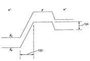
図4に示すエネルギー図は、図2および3に示す従来型デバイス100内の2つの接合部114および116のエネルギー障壁を示す。逆バイアスがかけられた接合部114の障壁は、平衡状態よりも増大し、順バイアスがかけられた接合部116の障壁は、平衡(ゼロ・ボルト・バイアス)状態に比べて低減する。図4では、逆バイアスがかけられた接合部114の空乏領域120の幅が122で示されており、順バイアスがかけられた接合部116のエネルギー障壁が124で示されている。
The energy diagram shown in FIG. 4 shows the energy barrier of the two
ここで図5を再度参照すると、逆バイアスがかけられた接合部14の空乏領域20を、順バイアスがかけられた接合部16の空乏領域に到達するようにすることができる場合、逆バイアスがかけられた接合部14の静電気の影響により、順バイアスがかけられた接合部16の、局所的には両空乏領域がそこでのみ出会う16.1のところの(図6の24で示す)エネルギー障壁が、図4に124で示す従来型デバイスのエネルギー障壁に比べて低下すると考えられる。
Referring again to FIG. 5, if the reverse
図6に示すように、順バイアスがかけられた接合部のところのエネルギー障壁24は、逆バイアスがかけられた接合部14から侵入する空乏領域20によってさらに低下する。この効果は一般に、パンチスルーとして知られており、通常は負の寄生効果として見なされているが、この場合にはその効果が、アバランシェ・エレクトロルミネセンス効果を高めるために積極的に使用される。
As shown in FIG. 6, the
パンチスルー効果は、図5の16.1で示すように局所化することができる。図5のデバイスでは、逆バイアスがかけられた接合部の空乏領域20が、横方向に離隔された隣接する接合部16に、局所的な明確に定義された部分またはインターフェース16.1内でパンチスルーする。隣接する接合部のエネルギー障壁24が、局所的に交差インターフェース16.1のところで低下し、それにより、接合部16のその部分16.1に、接合部の残りの部分よりも順バイアスがかかる。実際のところ、隣接する接合部16には、隣接する接合部全体を全面的に横切るキャリア注入を停止させるために、実際にわずかに逆バイアスをかけることができる。この場合、パンチスルー・インターフェース16.1は、隣接する接合部の、エネルギー障壁低下効果によって順バイアスがかけられている唯一の部分となり、逆バイアスがかけられた接合部の空乏領域への独占的なキャリア注入を引き起こす。デバイスをこのモードで用いることによって、バルクへのキャリア注入が逆バイアスがかけられた空乏領域に到達しないことによる損失が、より小さくなり得ると考えられ、さらに、エレクトロルミネセンス効率が向上し得ると考えられる。
The punch-through effect can be localized as shown at 16.1 in FIG. In the device of FIG. 5, the depleted
図7に示すように、本発明によるキャリア注入パンチスルー・デバイス10は、2端子デバイスとして動作させることもできる。この動作モードでは、端子構成18のp型バルク・コンタクトが不要である。
As shown in FIG. 7, the carrier injection punch-through
アバランシェ接合部へのキャリア注入を用いる利点は、従来型のn+p接合部と、それと比較してパンチスルーn+pn+構造について、空乏領域内のキャリア濃度プロファイルを調査することによって実証することができる。 The advantage of using carrier injection into an avalanche junction is demonstrated by investigating the carrier concentration profile in the depletion region for a conventional n + p junction and compared to a punch-through n + pn + structure Can do.
アバランシェ降伏状態にある従来型のn+p接合部に関するキャリア濃度プロファイルが、図8に示されており、パンチスルーn+pn+構造に関するキャリア濃度プロファイルが、図9に示されている。 A carrier concentration profile for a conventional n + p junction in an avalanche breakdown state is shown in FIG. 8, and a carrier concentration profile for a punch-through n + pn + structure is shown in FIG.
図8に示すデバイスは、空乏領域が比較的広く、アバランシェ利得が高く、p領域に隣接する空乏領域縁部で電子キャリア濃度が低い。アバランシェ増倍すべきキャリアは、p領域内で熱的に生成され、熱的に生成されたわずかな漏れ電流を構成する。このわずかな漏れ電流を比較的大きな逆アバランシェ電流に増大して光を発生させるために、アバランシェ利得は高くなければならない。 The device shown in FIG. 8 has a relatively wide depletion region, a high avalanche gain, and a low electron carrier concentration at the edge of the depletion region adjacent to the p region. The carriers to be avalanche-multiplied are thermally generated in the p region and constitute a slight leakage current generated thermally. In order to increase this small leakage current to a relatively large reverse avalanche current to generate light, the avalanche gain must be high.
一方、図9に示すパンチスルー・デバイス10の場合、アバランシェ増倍すべき電流は、順バイアスがかけられた接合部16からの注入電流であり、これは、熱的に生成された漏れ電流よりもずっと大きい。このデバイスでは、同じ光発生電流を達成するのに、必要なアバランシェ利得がより小さく、それにより空乏領域20がより狭くなり、その結果、デバイス10を通るキャリアの走行時間がより短くなり、したがってスイッチング応答がより速くなるはずである。空乏領域20がより狭いことにより、動作電圧もより低くなり、その結果、光発生過程の電力効率が向上し得る。
On the other hand, in the punch-through
やはり図9から明白なのは、パンチスルーの場合の方が、電子のキャリア濃度が大幅に高いことであり、それにより、特に放射性の直接キャリア(電子−正孔)再結合が電子/正孔キャリア濃度pn積に比例する場合、高電界空乏領域内でキャリアとフォノン、およびキャリアとキャリアの放射性相互作用(radiative interaction)が起こる確率がより高くなり得る。 It is also clear from FIG. 9 that the punch-through case has a much higher electron carrier concentration, so that especially the radioactive direct carrier (electron-hole) recombination is the electron / hole carrier concentration. When proportional to the pn product, there is a higher probability of radiative interactions between carriers and phonons and carriers and carriers within a high field depletion region.
パンチスルー・デバイス10の別の利点に、順バイアスがかけられた接合部16からキャリア注入される地点、すなわち順バイアスがかけられた接合部付近で、多数の「クールな」(低エネルギーの)電子が、空乏領域20の、多数の加速された「ホットな」(高エネルギーの)正孔があるのと同じ容積領域内にあり、それにより、放射性の直接遷移型キャリア再結合過程が向上することがあり得る。
Another advantage of the punch-through
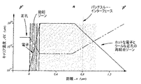
図10には、p+np+アバランシェ注入シリコン・エレクトロルミネセント・デバイス10の形をとる、本発明による一代替デバイスの概略図が示されている。図11には、デバイス10全体にわたる電界強度および分布の図が示されている。第1のp+n接合部14付近で、電界状態が、ホスト原子のイオン化および増倍を可能にするのに十分大きな大きさに達する。この領域を励起ゾーンと呼ぶ。中心のn領域でホスト原子がイオン化されるため、電界強度は、第2のp+n接合部16に到達するまで次第に減衰する。2つの接合部間の領域を、ドリフト・ゾーン30と呼ぶ。残りの短い電界減衰は、高ドープp+領域12.3内でのホスト・ドーパント原子のイオン化により占められる。特定のバイアス条件のため、また図12に示すように、高密度の低エネルギーの(クールな)正孔が、注入ゾーンとも呼ぶ第2のp+n接合部16からドリフト・ゾーン30に注入される。
FIG. 10 shows a schematic diagram of an alternative device according to the present invention in the form of a p + np + avalanche implanted
励起された両方の高エネルギー電子の分布が、励起接合部14に形成される。これらの電子は、デバイスのドリフト・ゾーン30を横断する。電子はその横断中、再結合中心または緩和中心として働くことのできる欠陥中心と相互作用することができる。注入ゾーン16から高密度の正孔が注入され、それが電子の方向とは反対方向に移動するので、ドリフト・ゾーン30全体において、高エネルギーのドリフトしている電子と低エネルギーの注入された正孔との間で再結合が起こり得る。
A distribution of both excited high energy electrons is formed at the
電子と正孔がドリフト領域30を横断しているときのそれらに関するキャリア・エネルギーの図が、図13に示されている。励起された電子は、その最大のホスト原子イオン化エネルギーをほぼ維持しながらドリフト・ゾーン30を横断し、そのエネルギーは約1.8eVである。電界強度は、電子のこのエネルギーをドリフト領域全体にわたって維持するのに十分なほど高い。電子は、パンチスルー・インターフェース(空乏領域20と注入用接合部の空乏領域が出会うインターフェース)に到達したとき、注入ゾーンに侵入し、しかもそのエネルギーを注入ゾーンの空乏領域の終わりまで維持すると考えることができる。高エネルギー電子は、そのエネルギーを失うまでに約150nmの平均的な平均自由行程長を有するので、大部分の電子は、注入接合部のほぼ中性のp+領域12.3にも侵入する。電子はそこで、p+領域12.3内に存在する多数の自由な低エネルギーの正孔と、後に相互作用することができる。注入用p+n接合部からドリフト・ゾーンに注入されている正孔は、エネルギーをすばやく獲得し、正孔にとって最大の、約2.3eVというホスト・シリコンのイオン化エネルギーを、150〜200nm以内で獲得すると考えられる。正孔はそのエネルギーを、ドリフト・ゾーン30の残りの部分を横断するときに維持する。高エネルギー電子と中エネルギーおよび高エネルギーの正孔との間の再結合過程が、ドリフト・ゾーン全体にわたって起こり得るが、この再結合過程は、エネルギーとキャリアの分布にそれほど影響を及ぼし得ない。
A diagram of the carrier energy associated with electrons and holes as they traverse the
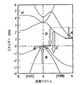
図14は、電子と正孔がドリフト・ゾーン30を横断するときのそれらに関する、対応する予測キャリア密度プロファイルを示す。ドリフト・ゾーン30内の高電界強度のため、電子はこのゾーンを、キャリア密度が大きく減少することなく(飽和速度に近い)高速で横断する。電子は、注入用接合部16から注入された高密度の正孔と相互作用して再結合するとき、全ての電子が正孔と再結合するまで、その濃度が急速に減衰し得ると考えることができる。この過程は、主としてドリフト・ゾーン30の終わりの部分内で起こり、さらには中性のp+領域内に及ぶこともある。同様に、高密度の低エネルギー正孔が接合部16から注入されて、横断している高エネルギーの放出電子と相互作用する。したがって、正孔濃度が接合部16から急速に減衰して、ある特定の中程度のレベルに至ると考えることができる。正孔は、ひとたび高電界ドリフト・ゾーン30に入ると飽和速度に達し、ドリフト・ゾーンの残りの部分の中を、それほど再結合せずにドリフトする。最大のエレクトロルミネセント収量を得るのに特に好都合な領域が、横断している高エネルギー電子と注入された低エネルギー正孔の両方の密度が高い、注入ゾーン16の付近になるものと現在予想されている。図13に示すキャリアの対応する予測エネルギーを考慮すると、図15に示す、それぞれ2.3eVおよび0.5eVのエネルギー遷移を生じさせるタイプDの遷移が起こり得ると現在予想されている。ドリフト領域30内のより深いところでは、約2.8〜2.9eVのタイプCの遷移が起こり得る。タイプAおよびBの遷移は、ドリフト・ゾーンの接合部14により近いさらに深い領域内で起こり得る。
FIG. 14 shows the corresponding predicted carrier density profile for electrons and holes as they traverse the
Claims (15)
前記ボディ内の、第1のドーピング・タイプをもつ前記ボディの第1の領域と第2のドーピング・タイプをもつ前記ボディの第2の領域との間に形成された、第1の接合領域と、
前記ボディ内の、前記ボディの前記第2の領域と前記第1のドーピング・タイプをもつ前記ボディの第3の領域との間に形成された、第2の接合領域と、
前記ボディに接続され、第2の接合領域の少なくとも一部に順バイアスをかけ、前記第1の接合領域が降伏モードとなるように第1の接合領域へと逆バイアスを印加するように構成された端子構成と
を備え、
前記逆バイアスがかけられた第1の接合領域に関連する第1の空乏領域が、前記第2の接合領域の少なくとも一部のエネルギー障壁を低くするために、前記第2の接合領域の前記順バイアスがかけられた少なくとも一部に関連する第2の空乏領域にパンチスルーするように構成されるとともに、キャリアを前記第2の接合領域の少なくとも一部から第1の空乏領域へと注入し、これによりデバイスにおけるエレクトロルミネセンス効果を向上させるように構成された
発光デバイス。
A body made of a semiconductor material;
A first junction region formed in the body between a first region of the body having a first doping type and a second region of the body having a second doping type; ,
A second junction region formed in the body between the second region of the body and the third region of the body having the first doping type;
Connected to the body, configured to apply a forward bias to at least a portion of the second junction region, and to apply a reverse bias to the first junction region so that the first junction region is in a breakdown mode. Terminal configuration,
A first depletion region associated with the reverse-biased first junction region reduces the energy barrier of at least a portion of the second junction region to reduce the order of the second junction region. Configured to punch through to a second depletion region associated with at least a portion of the bias, and to inject carriers from at least a portion of the second junction region into the first depletion region; A light emitting device configured to thereby improve the electroluminescence effect in the device.
Said second of said at least part of the bonding region is laterally spaced from the first junction region and a surface of the first junction region, the other region of the second junction region reverse biased The light emitting device according to claim 1.
The light emitting device according to claim 1, wherein the semiconductor material is a single crystal indirect transition semiconductor material.
The light emitting device of claim 3, wherein the semiconductor material comprises silicon.
The light emitting device according to claim 1, wherein the semiconductor material is a direct transition semiconductor material.
6. The light emitting device according to any one of claims 1 to 5, wherein the first doping type is n and the second doping type is p.
6. A light emitting device according to any one of the preceding claims, wherein the first doping type is p and the second doping type is n.
The light emitting device according to any one of claims 1 to 6, wherein the breakdown mode is one of an avalanche mode, a field emission mode, and a combination of an avalanche mode and a field emission mode.
The light emitting device according to any one of claims 1 to 8, wherein the first depletion region punches through to the second junction region.
A first terminal connected to the first region of the body for applying a voltage of a first polarity to the first region; and a third terminal of the body. The light emitting device according to any one of claims 1 to 9, comprising two terminals connected to a second terminal for applying a voltage of opposite polarity to the third region.
A first terminal connected to the first region of the body for applying a voltage of a first polarity to the first region of the body; and 3 of a second terminal connected to the third region for applying a voltage of opposite polarity to the third region, and a third terminal connected to the second region of the body The light emitting device according to claim 1, comprising one terminal.
第1のドーピング・タイプをもつ前記ボディの第1の領域と第2のドーピング・タイプをもつ前記ボディの第2の領域との間に形成された第1の接合領域と、前記ボディの前記第2の領域と前記第1のドーピング・タイプをもつ前記ボディの第3の領域との間のボディ内部に形成された第2の接合領域とを備える半導体材料のボディを供給するステップと、
前記第1の接合領域に逆バイアスをかけて降伏モードにするステップと、
前記第2の接合領域の少なくとも第1の部分に順バイアスをかけるステップと、
前記逆バイアスがかけられた第1の接合領域に関連する第1の空乏領域に、前記ボディの前記第2の領域を前記第2の接合領域の少なくとも一部のエネルギー障壁を低くするために、前記第2の接合領域の前記少なくとも第1の部分と関連する第2の空乏領域へとパンチスルーさせるとともに、キャリアを前記第2の接合領域の少なくとも第1の部分から第1の空乏領域へと注入させ、これによりデバイスにおけるエレクトロルミネセンス効果を向上させるステップと
を含む方法。
A method of operating a light emitting device,
A first junction region formed between a first region of the body having a first doping type and a second region of the body having a second doping type; and the first of the body. Providing a body of semiconductor material comprising a second junction region formed within the body between a second region and a third region of the body having the first doping type;
Reverse biasing the first junction region to a breakdown mode;
Applying a forward bias to at least a first portion of the second junction region;
In order to lower the energy barrier of at least part of the second junction region, the second region of the body in a first depletion region associated with the reverse-biased first junction region Punch-through to a second depletion region associated with the at least first portion of the second junction region, and carriers from at least the first portion of the second junction region to the first depletion region Implanting and thereby improving the electroluminescent effect in the device.
Wherein the second junction region reverse biased, by a first depletion region obtained by the punch-through, forward bias is Ru applied to the first portion of the second junction region, in claim 12 The method described.
14. The method according to claim 12 or 13, wherein the semiconductor material is a single crystal indirect transition semiconductor material.
Applications Claiming Priority (3)
| Application Number | Priority Date | Filing Date | Title |
|---|---|---|---|
| ZA2008/00593 | 2008-01-21 | ||
| ZA200800593 | 2008-01-21 | ||
| PCT/IB2009/050209 WO2009093177A1 (en) | 2008-01-21 | 2009-01-21 | Semiconductor light emitting device utilising punch-through effects |
Publications (3)
| Publication Number | Publication Date |
|---|---|
| JP2011510511A JP2011510511A (en) | 2011-03-31 |
| JP2011510511A5 JP2011510511A5 (en) | 2011-05-12 |
| JP5676273B2 true JP5676273B2 (en) | 2015-02-25 |
Family
ID=40586889
Family Applications (1)
| Application Number | Title | Priority Date | Filing Date |
|---|---|---|---|
| JP2010543598A Expired - Fee Related JP5676273B2 (en) | 2008-01-21 | 2009-01-21 | Semiconductor light-emitting device using punch-through effect |
Country Status (5)
| Country | Link |
|---|---|
| US (1) | US8759845B2 (en) |
| EP (1) | EP2245676A1 (en) |
| JP (1) | JP5676273B2 (en) |
| WO (1) | WO2009093177A1 (en) |
| ZA (1) | ZA201004753B (en) |
Families Citing this family (8)
| Publication number | Priority date | Publication date | Assignee | Title |
|---|---|---|---|---|
| WO2009057075A2 (en) | 2007-11-01 | 2009-05-07 | Insiava (Pty) Ltd | Optoelectronic device with light directing arrangement and method of forming the arrangement |
| US8759845B2 (en) | 2008-01-21 | 2014-06-24 | Insiava (Pty) Limited | Semiconductor light emitting device utilising punch-through effects |
| ATE523900T1 (en) * | 2008-02-01 | 2011-09-15 | Insiava Pty Ltd | LIGHT-EMITTING SEMICONDUCTOR COMPONENT WITH HETEROJUNCTIONS |
| CN102292834A (en) | 2008-12-15 | 2011-12-21 | 因西亚瓦(控股)有限公司 | Silicon light emitting device utilising reach-through effects |
| US9117970B2 (en) | 2010-01-22 | 2015-08-25 | Insiava (Pty) Limited | Silicon light emitting device and method of fabricating same |
| JP5665504B2 (en) * | 2010-11-24 | 2015-02-04 | キヤノン株式会社 | Vertical cavity surface emitting laser and vertical cavity surface emitting laser array |
| EP2756527B1 (en) | 2011-09-16 | 2015-11-18 | Insiava (Pty) Limited | Near infrared light source in bulk silicon |
| WO2018049434A2 (en) | 2016-09-06 | 2018-03-15 | University Of South Africa | Optimised 650 nm silicon avalanche led |
Family Cites Families (16)
| Publication number | Priority date | Publication date | Assignee | Title |
|---|---|---|---|---|
| JPS60167390A (en) | 1984-02-09 | 1985-08-30 | Matsushita Electric Ind Co Ltd | Semiconductor light-emitting element |
| JPS63181486A (en) | 1987-01-23 | 1988-07-26 | Hiroshima Univ | Semiconductor light emitting device |
| US5136353A (en) * | 1990-05-10 | 1992-08-04 | The University Of Colorado Foundation, Inc. | Optical switch |
| US5510627A (en) * | 1994-06-29 | 1996-04-23 | The United States Of America As Represented By The Secretary Of The Navy | Infrared-to-visible converter |
| US5994720A (en) * | 1996-03-04 | 1999-11-30 | University Of Pretoria | Indirect bandgap semiconductor optoelectronic device |
| US6111271A (en) * | 1996-03-28 | 2000-08-29 | University Of Pretoria | Optoelectronic device with separately controllable carrier injection means |
| JP4024431B2 (en) * | 1999-07-23 | 2007-12-19 | 株式会社東芝 | Bidirectional semiconductor light emitting device and optical transmission device |
| JP2002246639A (en) * | 2001-02-20 | 2002-08-30 | Fujitsu Ltd | Semiconductor light emitting device |
| EP1656701A4 (en) * | 2003-08-22 | 2007-10-10 | Univ Illinois | Semiconductor device and method |
| EP2674991A1 (en) * | 2007-10-08 | 2013-12-18 | Insiava (Pty) Limited | Silicon light emitting device with carrier injection |
| WO2009057075A2 (en) * | 2007-11-01 | 2009-05-07 | Insiava (Pty) Ltd | Optoelectronic device with light directing arrangement and method of forming the arrangement |
| US8759845B2 (en) | 2008-01-21 | 2014-06-24 | Insiava (Pty) Limited | Semiconductor light emitting device utilising punch-through effects |
| ATE523900T1 (en) * | 2008-02-01 | 2011-09-15 | Insiava Pty Ltd | LIGHT-EMITTING SEMICONDUCTOR COMPONENT WITH HETEROJUNCTIONS |
| CN102292834A (en) * | 2008-12-15 | 2011-12-21 | 因西亚瓦(控股)有限公司 | Silicon light emitting device utilising reach-through effects |
| US8395226B2 (en) * | 2009-01-27 | 2013-03-12 | Insiava (Pty) Limited | Microchip-based MOEMS and waveguide device |
| US9117970B2 (en) * | 2010-01-22 | 2015-08-25 | Insiava (Pty) Limited | Silicon light emitting device and method of fabricating same |
-
2009
- 2009-01-21 US US12/863,743 patent/US8759845B2/en not_active Expired - Fee Related
- 2009-01-21 JP JP2010543598A patent/JP5676273B2/en not_active Expired - Fee Related
- 2009-01-21 WO PCT/IB2009/050209 patent/WO2009093177A1/en active Application Filing
- 2009-01-21 EP EP09703175A patent/EP2245676A1/en not_active Ceased
-
2010
- 2010-07-06 ZA ZA2010/04753A patent/ZA201004753B/en unknown
Also Published As
| Publication number | Publication date |
|---|---|
| EP2245676A1 (en) | 2010-11-03 |
| ZA201004753B (en) | 2011-08-31 |
| JP2011510511A (en) | 2011-03-31 |
| US20110031893A1 (en) | 2011-02-10 |
| WO2009093177A1 (en) | 2009-07-30 |
| US8759845B2 (en) | 2014-06-24 |
Similar Documents
| Publication | Publication Date | Title |
|---|---|---|
| JP5676273B2 (en) | Semiconductor light-emitting device using punch-through effect | |
| KR102357920B1 (en) | A p-n junction optoelectronic device for ionizing dopants by field effect | |
| US9306113B2 (en) | Silicon light emitting device utilising reach-through effects | |
| US8362679B2 (en) | Silicon light emitting device with carrier injection | |
| US20140225059A1 (en) | LED with Improved Injection Efficiency | |
| US8674382B2 (en) | Semiconductor light emitting device comprising heterojunction | |
| TW200618430A (en) | Semiconductor heterostructure | |
| EP2919282B1 (en) | Nitride semiconductor stacked body and semiconductor light emitting device comprising the same | |
| US11631780B2 (en) | Light-emitting metal-oxide-semiconductor devices and associated systems, devices, and methods | |
| CN112466954A (en) | Semiconductor device and manufacturing method thereof | |
| CN108701729A (en) | Semiconductor device including pinned photodiode structure | |
| Ali et al. | Design Analysis of Linear Graded Quantum barriers in Ultavoilet-C Laser Diodes | |
| JP2015163693A (en) | Luminescent material, production method of luminescent material, light emitter and light emitting device | |
| WO2009093170A1 (en) | Silicon light emitting device utilising reach-through effects | |
| Kim et al. | P–N Junction Diode: I–V Behavior and Applications | |
| WO2009150628A1 (en) | Silicon light emitting device utilizing radiative carrier recombination in oxide |
Legal Events
| Date | Code | Title | Description |
|---|---|---|---|
| A621 | Written request for application examination |
Free format text: JAPANESE INTERMEDIATE CODE: A621 Effective date: 20111208 |
|
| RD04 | Notification of resignation of power of attorney |
Free format text: JAPANESE INTERMEDIATE CODE: A7424 Effective date: 20120710 |
|
| A977 | Report on retrieval |
Free format text: JAPANESE INTERMEDIATE CODE: A971007 Effective date: 20130306 |
|
| A131 | Notification of reasons for refusal |
Free format text: JAPANESE INTERMEDIATE CODE: A131 Effective date: 20130402 |
|
| A601 | Written request for extension of time |
Free format text: JAPANESE INTERMEDIATE CODE: A601 Effective date: 20130702 |
|
| A602 | Written permission of extension of time |
Free format text: JAPANESE INTERMEDIATE CODE: A602 Effective date: 20130709 |
|
| A521 | Request for written amendment filed |
Free format text: JAPANESE INTERMEDIATE CODE: A523 Effective date: 20131002 |
|
| A131 | Notification of reasons for refusal |
Free format text: JAPANESE INTERMEDIATE CODE: A131 Effective date: 20140304 |
|
| A521 | Request for written amendment filed |
Free format text: JAPANESE INTERMEDIATE CODE: A523 Effective date: 20140603 |
|
| TRDD | Decision of grant or rejection written | ||
| A01 | Written decision to grant a patent or to grant a registration (utility model) |
Free format text: JAPANESE INTERMEDIATE CODE: A01 Effective date: 20141202 |
|
| A61 | First payment of annual fees (during grant procedure) |
Free format text: JAPANESE INTERMEDIATE CODE: A61 Effective date: 20141225 |
|
| R150 | Certificate of patent or registration of utility model |
Ref document number: 5676273 Country of ref document: JP Free format text: JAPANESE INTERMEDIATE CODE: R150 |
|
| R250 | Receipt of annual fees |
Free format text: JAPANESE INTERMEDIATE CODE: R250 |
|
| R250 | Receipt of annual fees |
Free format text: JAPANESE INTERMEDIATE CODE: R250 |
|
| R250 | Receipt of annual fees |
Free format text: JAPANESE INTERMEDIATE CODE: R250 |
|
| LAPS | Cancellation because of no payment of annual fees |