JP5669752B2 - Reducing threshold voltage variation by reducing deposition non-uniformity in transistors with channel semiconductor alloys - Google Patents
Reducing threshold voltage variation by reducing deposition non-uniformity in transistors with channel semiconductor alloys Download PDFInfo
- Publication number
- JP5669752B2 JP5669752B2 JP2011542725A JP2011542725A JP5669752B2 JP 5669752 B2 JP5669752 B2 JP 5669752B2 JP 2011542725 A JP2011542725 A JP 2011542725A JP 2011542725 A JP2011542725 A JP 2011542725A JP 5669752 B2 JP5669752 B2 JP 5669752B2
- Authority
- JP
- Japan
- Prior art keywords
- silicon
- forming
- semiconductor
- layer
- alloy
- Prior art date
- Legal status (The legal status is an assumption and is not a legal conclusion. Google has not performed a legal analysis and makes no representation as to the accuracy of the status listed.)
- Active
Links
- 239000004065 semiconductor Substances 0.000 title claims description 194
- 229910045601 alloy Inorganic materials 0.000 title claims description 74
- 239000000956 alloy Substances 0.000 title claims description 74
- 230000008021 deposition Effects 0.000 title claims description 34
- 238000000034 method Methods 0.000 claims description 100
- 239000000463 material Substances 0.000 claims description 87
- XUIMIQQOPSSXEZ-UHFFFAOYSA-N Silicon Chemical compound [Si] XUIMIQQOPSSXEZ-UHFFFAOYSA-N 0.000 claims description 80
- 239000010703 silicon Substances 0.000 claims description 80
- 230000008569 process Effects 0.000 claims description 62
- 229910052710 silicon Inorganic materials 0.000 claims description 62
- 238000005530 etching Methods 0.000 claims description 34
- 238000002955 isolation Methods 0.000 claims description 31
- 239000002019 doping agent Substances 0.000 claims description 23
- 238000002513 implantation Methods 0.000 claims description 23
- 239000007772 electrode material Substances 0.000 claims description 21
- 229910052751 metal Inorganic materials 0.000 claims description 21
- 239000002184 metal Substances 0.000 claims description 21
- 229910000927 Ge alloy Inorganic materials 0.000 claims description 16
- 229910000676 Si alloy Inorganic materials 0.000 claims description 16
- WGTYBPLFGIVFAS-UHFFFAOYSA-M tetramethylammonium hydroxide Chemical compound [OH-].C[N+](C)(C)C WGTYBPLFGIVFAS-UHFFFAOYSA-M 0.000 claims description 14
- 239000003989 dielectric material Substances 0.000 claims description 13
- 238000000059 patterning Methods 0.000 claims description 11
- 238000003631 wet chemical etching Methods 0.000 claims description 8
- 238000000926 separation method Methods 0.000 claims description 3
- 238000004519 manufacturing process Methods 0.000 description 50
- VYPSYNLAJGMNEJ-UHFFFAOYSA-N Silicium dioxide Chemical compound O=[Si]=O VYPSYNLAJGMNEJ-UHFFFAOYSA-N 0.000 description 48
- 238000000151 deposition Methods 0.000 description 36
- 239000000377 silicon dioxide Substances 0.000 description 24
- 235000012239 silicon dioxide Nutrition 0.000 description 24
- 238000012545 processing Methods 0.000 description 12
- 230000003647 oxidation Effects 0.000 description 11
- 238000007254 oxidation reaction Methods 0.000 description 11
- 239000000758 substrate Substances 0.000 description 10
- 239000000203 mixture Substances 0.000 description 8
- 229910021420 polycrystalline silicon Inorganic materials 0.000 description 8
- 229910052732 germanium Inorganic materials 0.000 description 7
- GNPVGFCGXDBREM-UHFFFAOYSA-N germanium atom Chemical compound [Ge] GNPVGFCGXDBREM-UHFFFAOYSA-N 0.000 description 7
- 239000000126 substance Substances 0.000 description 7
- KRHYYFGTRYWZRS-UHFFFAOYSA-N Fluorane Chemical compound F KRHYYFGTRYWZRS-UHFFFAOYSA-N 0.000 description 6
- 229910052581 Si3N4 Inorganic materials 0.000 description 6
- 238000005516 engineering process Methods 0.000 description 6
- 230000005669 field effect Effects 0.000 description 6
- 238000001459 lithography Methods 0.000 description 6
- HQVNEWCFYHHQES-UHFFFAOYSA-N silicon nitride Chemical compound N12[Si]34N5[Si]62N3[Si]51N64 HQVNEWCFYHHQES-UHFFFAOYSA-N 0.000 description 6
- 239000002210 silicon-based material Substances 0.000 description 6
- 230000008878 coupling Effects 0.000 description 5
- 238000010168 coupling process Methods 0.000 description 5
- 238000005859 coupling reaction Methods 0.000 description 5
- 238000005137 deposition process Methods 0.000 description 5
- NRTOMJZYCJJWKI-UHFFFAOYSA-N Titanium nitride Chemical compound [Ti]#N NRTOMJZYCJJWKI-UHFFFAOYSA-N 0.000 description 4
- TWNQGVIAIRXVLR-UHFFFAOYSA-N oxo(oxoalumanyloxy)alumane Chemical compound O=[Al]O[Al]=O TWNQGVIAIRXVLR-UHFFFAOYSA-N 0.000 description 4
- 238000000137 annealing Methods 0.000 description 3
- 239000002800 charge carrier Substances 0.000 description 3
- 238000012856 packing Methods 0.000 description 3
- 238000013459 approach Methods 0.000 description 2
- 230000015572 biosynthetic process Effects 0.000 description 2
- 238000005229 chemical vapour deposition Methods 0.000 description 2
- 230000000694 effects Effects 0.000 description 2
- 125000001475 halogen functional group Chemical group 0.000 description 2
- 239000007943 implant Substances 0.000 description 2
- 238000009413 insulation Methods 0.000 description 2
- 238000005468 ion implantation Methods 0.000 description 2
- 230000009467 reduction Effects 0.000 description 2
- 229910052814 silicon oxide Inorganic materials 0.000 description 2
- 238000003860 storage Methods 0.000 description 2
- 229910004129 HfSiO Inorganic materials 0.000 description 1
- 230000003213 activating effect Effects 0.000 description 1
- 230000006978 adaptation Effects 0.000 description 1
- 239000003990 capacitor Substances 0.000 description 1
- 239000004020 conductor Substances 0.000 description 1
- 239000013078 crystal Substances 0.000 description 1
- 230000003247 decreasing effect Effects 0.000 description 1
- 230000001419 dependent effect Effects 0.000 description 1
- 238000013461 design Methods 0.000 description 1
- 239000006185 dispersion Substances 0.000 description 1
- 230000002708 enhancing effect Effects 0.000 description 1
- 230000001747 exhibiting effect Effects 0.000 description 1
- CJNBYAVZURUTKZ-UHFFFAOYSA-N hafnium(iv) oxide Chemical compound O=[Hf]=O CJNBYAVZURUTKZ-UHFFFAOYSA-N 0.000 description 1
- 230000000977 initiatory effect Effects 0.000 description 1
- 239000011810 insulating material Substances 0.000 description 1
- 239000012212 insulator Substances 0.000 description 1
- 230000007246 mechanism Effects 0.000 description 1
- 150000002739 metals Chemical class 0.000 description 1
- 238000012986 modification Methods 0.000 description 1
- 230000004048 modification Effects 0.000 description 1
- BPUBBGLMJRNUCC-UHFFFAOYSA-N oxygen(2-);tantalum(5+) Chemical compound [O-2].[O-2].[O-2].[O-2].[O-2].[Ta+5].[Ta+5] BPUBBGLMJRNUCC-UHFFFAOYSA-N 0.000 description 1
- RVTZCBVAJQQJTK-UHFFFAOYSA-N oxygen(2-);zirconium(4+) Chemical compound [O-2].[O-2].[Zr+4] RVTZCBVAJQQJTK-UHFFFAOYSA-N 0.000 description 1
- 238000000623 plasma-assisted chemical vapour deposition Methods 0.000 description 1
- 238000005498 polishing Methods 0.000 description 1
- 239000002243 precursor Substances 0.000 description 1
- 229910021332 silicide Inorganic materials 0.000 description 1
- FVBUAEGBCNSCDD-UHFFFAOYSA-N silicide(4-) Chemical group [Si-4] FVBUAEGBCNSCDD-UHFFFAOYSA-N 0.000 description 1
- 125000006850 spacer group Chemical group 0.000 description 1
- PWYYWQHXAPXYMF-UHFFFAOYSA-N strontium(2+) Chemical compound [Sr+2] PWYYWQHXAPXYMF-UHFFFAOYSA-N 0.000 description 1
- 238000004381 surface treatment Methods 0.000 description 1
- 238000012876 topography Methods 0.000 description 1
- 230000005641 tunneling Effects 0.000 description 1
- 229910001928 zirconium oxide Inorganic materials 0.000 description 1
Images


Classifications
-
- H—ELECTRICITY
- H01—ELECTRIC ELEMENTS
- H01L—SEMICONDUCTOR DEVICES NOT COVERED BY CLASS H10
- H01L21/00—Processes or apparatus adapted for the manufacture or treatment of semiconductor or solid state devices or of parts thereof
- H01L21/70—Manufacture or treatment of devices consisting of a plurality of solid state components formed in or on a common substrate or of parts thereof; Manufacture of integrated circuit devices or of parts thereof
- H01L21/77—Manufacture or treatment of devices consisting of a plurality of solid state components or integrated circuits formed in, or on, a common substrate
- H01L21/78—Manufacture or treatment of devices consisting of a plurality of solid state components or integrated circuits formed in, or on, a common substrate with subsequent division of the substrate into plural individual devices
- H01L21/82—Manufacture or treatment of devices consisting of a plurality of solid state components or integrated circuits formed in, or on, a common substrate with subsequent division of the substrate into plural individual devices to produce devices, e.g. integrated circuits, each consisting of a plurality of components
- H01L21/822—Manufacture or treatment of devices consisting of a plurality of solid state components or integrated circuits formed in, or on, a common substrate with subsequent division of the substrate into plural individual devices to produce devices, e.g. integrated circuits, each consisting of a plurality of components the substrate being a semiconductor, using silicon technology
- H01L21/8232—Field-effect technology
- H01L21/8234—MIS technology, i.e. integration processes of field effect transistors of the conductor-insulator-semiconductor type
- H01L21/8238—Complementary field-effect transistors, e.g. CMOS
-
- H—ELECTRICITY
- H01—ELECTRIC ELEMENTS
- H01L—SEMICONDUCTOR DEVICES NOT COVERED BY CLASS H10
- H01L21/00—Processes or apparatus adapted for the manufacture or treatment of semiconductor or solid state devices or of parts thereof
- H01L21/70—Manufacture or treatment of devices consisting of a plurality of solid state components formed in or on a common substrate or of parts thereof; Manufacture of integrated circuit devices or of parts thereof
- H01L21/77—Manufacture or treatment of devices consisting of a plurality of solid state components or integrated circuits formed in, or on, a common substrate
- H01L21/78—Manufacture or treatment of devices consisting of a plurality of solid state components or integrated circuits formed in, or on, a common substrate with subsequent division of the substrate into plural individual devices
- H01L21/82—Manufacture or treatment of devices consisting of a plurality of solid state components or integrated circuits formed in, or on, a common substrate with subsequent division of the substrate into plural individual devices to produce devices, e.g. integrated circuits, each consisting of a plurality of components
- H01L21/822—Manufacture or treatment of devices consisting of a plurality of solid state components or integrated circuits formed in, or on, a common substrate with subsequent division of the substrate into plural individual devices to produce devices, e.g. integrated circuits, each consisting of a plurality of components the substrate being a semiconductor, using silicon technology
- H01L21/8232—Field-effect technology
- H01L21/8234—MIS technology, i.e. integration processes of field effect transistors of the conductor-insulator-semiconductor type
- H01L21/823412—MIS technology, i.e. integration processes of field effect transistors of the conductor-insulator-semiconductor type with a particular manufacturing method of the channel structures, e.g. channel implants, halo or pocket implants, or channel materials
-
- H—ELECTRICITY
- H01—ELECTRIC ELEMENTS
- H01L—SEMICONDUCTOR DEVICES NOT COVERED BY CLASS H10
- H01L21/00—Processes or apparatus adapted for the manufacture or treatment of semiconductor or solid state devices or of parts thereof
- H01L21/70—Manufacture or treatment of devices consisting of a plurality of solid state components formed in or on a common substrate or of parts thereof; Manufacture of integrated circuit devices or of parts thereof
- H01L21/77—Manufacture or treatment of devices consisting of a plurality of solid state components or integrated circuits formed in, or on, a common substrate
- H01L21/78—Manufacture or treatment of devices consisting of a plurality of solid state components or integrated circuits formed in, or on, a common substrate with subsequent division of the substrate into plural individual devices
- H01L21/82—Manufacture or treatment of devices consisting of a plurality of solid state components or integrated circuits formed in, or on, a common substrate with subsequent division of the substrate into plural individual devices to produce devices, e.g. integrated circuits, each consisting of a plurality of components
- H01L21/822—Manufacture or treatment of devices consisting of a plurality of solid state components or integrated circuits formed in, or on, a common substrate with subsequent division of the substrate into plural individual devices to produce devices, e.g. integrated circuits, each consisting of a plurality of components the substrate being a semiconductor, using silicon technology
- H01L21/8232—Field-effect technology
- H01L21/8234—MIS technology, i.e. integration processes of field effect transistors of the conductor-insulator-semiconductor type
- H01L21/823437—MIS technology, i.e. integration processes of field effect transistors of the conductor-insulator-semiconductor type with a particular manufacturing method of the gate conductors, e.g. particular materials, shapes
- H01L21/82345—MIS technology, i.e. integration processes of field effect transistors of the conductor-insulator-semiconductor type with a particular manufacturing method of the gate conductors, e.g. particular materials, shapes gate conductors with different gate conductor materials or different gate conductor implants, e.g. dual gate structures
-
- H—ELECTRICITY
- H01—ELECTRIC ELEMENTS
- H01L—SEMICONDUCTOR DEVICES NOT COVERED BY CLASS H10
- H01L21/00—Processes or apparatus adapted for the manufacture or treatment of semiconductor or solid state devices or of parts thereof
- H01L21/70—Manufacture or treatment of devices consisting of a plurality of solid state components formed in or on a common substrate or of parts thereof; Manufacture of integrated circuit devices or of parts thereof
- H01L21/77—Manufacture or treatment of devices consisting of a plurality of solid state components or integrated circuits formed in, or on, a common substrate
- H01L21/78—Manufacture or treatment of devices consisting of a plurality of solid state components or integrated circuits formed in, or on, a common substrate with subsequent division of the substrate into plural individual devices
- H01L21/82—Manufacture or treatment of devices consisting of a plurality of solid state components or integrated circuits formed in, or on, a common substrate with subsequent division of the substrate into plural individual devices to produce devices, e.g. integrated circuits, each consisting of a plurality of components
- H01L21/822—Manufacture or treatment of devices consisting of a plurality of solid state components or integrated circuits formed in, or on, a common substrate with subsequent division of the substrate into plural individual devices to produce devices, e.g. integrated circuits, each consisting of a plurality of components the substrate being a semiconductor, using silicon technology
- H01L21/8232—Field-effect technology
- H01L21/8234—MIS technology, i.e. integration processes of field effect transistors of the conductor-insulator-semiconductor type
- H01L21/8238—Complementary field-effect transistors, e.g. CMOS
- H01L21/823807—Complementary field-effect transistors, e.g. CMOS with a particular manufacturing method of the channel structures, e.g. channel implants, halo or pocket implants, or channel materials
-
- H—ELECTRICITY
- H01—ELECTRIC ELEMENTS
- H01L—SEMICONDUCTOR DEVICES NOT COVERED BY CLASS H10
- H01L21/00—Processes or apparatus adapted for the manufacture or treatment of semiconductor or solid state devices or of parts thereof
- H01L21/70—Manufacture or treatment of devices consisting of a plurality of solid state components formed in or on a common substrate or of parts thereof; Manufacture of integrated circuit devices or of parts thereof
- H01L21/77—Manufacture or treatment of devices consisting of a plurality of solid state components or integrated circuits formed in, or on, a common substrate
- H01L21/78—Manufacture or treatment of devices consisting of a plurality of solid state components or integrated circuits formed in, or on, a common substrate with subsequent division of the substrate into plural individual devices
- H01L21/82—Manufacture or treatment of devices consisting of a plurality of solid state components or integrated circuits formed in, or on, a common substrate with subsequent division of the substrate into plural individual devices to produce devices, e.g. integrated circuits, each consisting of a plurality of components
- H01L21/822—Manufacture or treatment of devices consisting of a plurality of solid state components or integrated circuits formed in, or on, a common substrate with subsequent division of the substrate into plural individual devices to produce devices, e.g. integrated circuits, each consisting of a plurality of components the substrate being a semiconductor, using silicon technology
- H01L21/8232—Field-effect technology
- H01L21/8234—MIS technology, i.e. integration processes of field effect transistors of the conductor-insulator-semiconductor type
- H01L21/8238—Complementary field-effect transistors, e.g. CMOS
- H01L21/823828—Complementary field-effect transistors, e.g. CMOS with a particular manufacturing method of the gate conductors, e.g. particular materials, shapes
- H01L21/823842—Complementary field-effect transistors, e.g. CMOS with a particular manufacturing method of the gate conductors, e.g. particular materials, shapes gate conductors with different gate conductor materials or different gate conductor implants, e.g. dual gate structures
-
- H—ELECTRICITY
- H01—ELECTRIC ELEMENTS
- H01L—SEMICONDUCTOR DEVICES NOT COVERED BY CLASS H10
- H01L21/00—Processes or apparatus adapted for the manufacture or treatment of semiconductor or solid state devices or of parts thereof
- H01L21/70—Manufacture or treatment of devices consisting of a plurality of solid state components formed in or on a common substrate or of parts thereof; Manufacture of integrated circuit devices or of parts thereof
- H01L21/77—Manufacture or treatment of devices consisting of a plurality of solid state components or integrated circuits formed in, or on, a common substrate
- H01L21/78—Manufacture or treatment of devices consisting of a plurality of solid state components or integrated circuits formed in, or on, a common substrate with subsequent division of the substrate into plural individual devices
- H01L21/82—Manufacture or treatment of devices consisting of a plurality of solid state components or integrated circuits formed in, or on, a common substrate with subsequent division of the substrate into plural individual devices to produce devices, e.g. integrated circuits, each consisting of a plurality of components
- H01L21/84—Manufacture or treatment of devices consisting of a plurality of solid state components or integrated circuits formed in, or on, a common substrate with subsequent division of the substrate into plural individual devices to produce devices, e.g. integrated circuits, each consisting of a plurality of components the substrate being other than a semiconductor body, e.g. being an insulating body
Description
概して、本開示は、金属含有電極と二酸化シリコン及びシリコン窒化物のようなゲート誘電体に比べて大きな誘電率の高k誘電体とを含む高容量性ゲート構造を備えた進歩的なトランジスタ要素を含む洗練された集積回路に関する。 In general, the present disclosure provides an advanced transistor element with a high-capacitance gate structure that includes a metal-containing electrode and a high-k dielectric with a large dielectric constant compared to a gate dielectric such as silicon dioxide and silicon nitride. Including a sophisticated integrated circuit.
CPU、記憶デバイス、ASIC(特定用途向け集積回路)等の高度な集積回路の製造は、指定された回路レイアウトに従い所与のチップ区域上に形成されるべき多数の回路要素を必要とし、電界効果トランジスタは、集積回路の性能を実質的に決定する回路要素の1つの重要な種類を代表する。概して多くのプロセス技術が現在のところ実施されており、電界効果トランジスタを含め多くの種類の複雑な回路に対しては、動作速度及び/又は電力消費及び/又は費用効果を考慮した優れた特性により、現在のところMOS技術が最も有望な手法の1つである。例えばMOS技術を用いた複雑な集積回路の製造においては、何百万のトランジスタ、例えばnチャネルトランジスタ及び/又はpチャネルトランジスタが結晶性の半導体層を含む基板上に形成される。電界効果トランジスタは、nチャネルトランジスタ又はpチャネルトランジスタのいずれが考慮されているかにかかわらず、典型的には複数の所謂pn接合を備えており、pn接合は、ドレイン及びソース領域と称される高濃度にドープされた領域とその高濃度にドープされた領域に隣接して配置される低濃度にドープされた又は非ドープの領域、例えばチャネル領域との界面によって形成されている。電界効果トランジスタにおいては、チャネル領域の伝導性、即ち伝導性チャネルの駆動電流能力は、チャネル領域に隣接して形成され且つ薄い絶縁層によってチャネル領域から隔てられているゲート電極によって制御される。ゲート電極への適切な制御電圧の印加による伝導性チャネルが形成されている場合、チャネル領域の伝導性は、ドーパント濃度、電荷キャリアの移動度に依存し、そしてトランジスタ幅方向におけるチャネル領域の所与の拡張に対しては、チャネル長とも称されるソース及びドレイン領域間の距離にも依存する。従って、ゲート電極に制御電圧が印加されている場合に絶縁層の下方に伝導性チャネルを急速に生成する能力と共に、チャネル領域の伝導性は、MOSトランジスタの性能に大きな影響を与える。このように、ゲート電極の伝導性に依存するチャネルを生成する速度、及びチャネル抵抗率がトランジスタ特性を実質的に決定するので、チャネル長のスケーリング(scaling)並びにそれに関連してチャネル抵抗率の減少及びゲート抵抗率の減少は、集積回路の動作速度の増大を達成するための支配的な設計基準である。 The manufacture of advanced integrated circuits such as CPUs, storage devices, application specific integrated circuits (ASICs), etc. requires a large number of circuit elements to be formed on a given chip area according to the specified circuit layout, and the field effect Transistors represent one important type of circuit element that substantially determines the performance of an integrated circuit. In general, many process technologies are currently implemented, and for many types of complex circuits, including field effect transistors, due to their superior characteristics considering operating speed and / or power consumption and / or cost effectiveness. Currently, MOS technology is one of the most promising approaches. For example, in the manufacture of complex integrated circuits using MOS technology, millions of transistors, such as n-channel transistors and / or p-channel transistors, are formed on a substrate including a crystalline semiconductor layer. A field effect transistor typically includes a plurality of so-called pn junctions, regardless of whether an n-channel transistor or a p-channel transistor is considered, and the pn junction is a high-level region called a drain and source region. It is formed by an interface between a lightly doped region and a lightly doped or undoped region, such as a channel region, disposed adjacent to the heavily doped region. In a field effect transistor, the conductivity of the channel region, i.e., the drive current capability of the conductive channel, is controlled by a gate electrode formed adjacent to the channel region and separated from the channel region by a thin insulating layer. When a conductive channel is formed by applying an appropriate control voltage to the gate electrode, the conductivity of the channel region depends on the dopant concentration, charge carrier mobility, and the given channel region in the transistor width direction. This extension also depends on the distance between the source and drain regions, also called channel length. Therefore, the conductivity of the channel region, along with the ability to rapidly create a conductive channel below the insulating layer when a control voltage is applied to the gate electrode, greatly affects the performance of the MOS transistor. Thus, the channel generation rate, which depends on the conductivity of the gate electrode, and the channel resistivity substantially determine the transistor characteristics, so channel length scaling and associated channel resistivity reduction. And decreasing gate resistivity is the dominant design criterion for achieving increased operating speed of integrated circuits.
現在、シリコンの実質的に無制限な入手可能性、シリコン並びに関連する材質及びプロセスの十分に理解された特性、並びにこの50年を超えて蓄積されてきた経験により、集積回路の大半はシリコンに基いて製造されている。従っておそらくシリコンは、大量生産品に対して設計される回路世代のための予測可能な将来において選択される材質であり続けるであろう。半導体デバイスを製造する場合におけるシリコンの重要性に対する1つの理由は、互いに異なる領域の信頼性のある電気的絶縁を可能にするシリコン/二酸化シリコン界面の優れた特性にあった。シリコン/二酸化シリコン界面は高温で安定であり従って、例えば界面の電気的特性を犠牲にすることなくドーパントを活性化し且つ結晶損傷を取り除くための焼鈍サイクルに対して要求されるような後続の高温処理の実行を可能にする。 Today, due to the virtually unlimited availability of silicon, the well-understood properties of silicon and related materials and processes, and the experience accumulated over the last 50 years, the majority of integrated circuits are based on silicon. And manufactured. Therefore, silicon will likely remain the material of choice in the predictable future for circuit generations designed for mass production. One reason for the importance of silicon in manufacturing semiconductor devices has been the excellent properties of the silicon / silicon dioxide interface that allows reliable electrical isolation of different regions. The silicon / silicon dioxide interface is stable at high temperatures, so that subsequent high-temperature processing, such as required for annealing cycles to activate dopants and remove crystal damage without sacrificing the electrical properties of the interface Enable execution.
上述した理由のため、二酸化シリコンは、大抵は多結晶シリコン又は他の金属含有材質からなるゲート電極をシリコンチャネル領域から隔てるゲート絶縁層として、電界効果トランジスタにおいて好適に用いられる。電界効果トランジスタのデバイス性能を着実に向上させることにおいて、スイッチング速度及び駆動電流能力を改善するために、チャネル領域の長さが絶えず減少させられてきた。トランジスタの動作は、所与の供給電圧に対して望ましい駆動電流を供給するのに十分高い電荷密度にまでチャネル領域の表面を反転させるためにゲート電極に供給される電圧によって制御されるので、ゲート電極、チャネル領域及びそれらの間に配置される二酸化シリコンにより形成されるキャパシタによって提供されるある程度の容量性結合は維持される必要がある。チャネル長を減少させることは、トランジスタ動作の間の所謂短チャネル挙動を避けるために大きな容量性結合を必要とすることが判明している。短チャネル挙動は、漏れ電流の増大とスレッショルド電圧のチャネル長への明白な依存とをもたらす可能性がある。比較的低い供給電圧及びそれにより低下させられたスレッショルド電圧を有する積極的に縮小化されたトランジスタデバイスは、漏れ電流の指数関数的な増大に悩まされることがある一方で、ゲート電極のチャネル領域に対する強化された容量性結合を必要とする。このように二酸化シリコン層の厚みは、ゲートとチャネル領域の間で要求される容量を提供するためにこれに対応して減少させられる必要がある。例えば約0.08μmのチャネル長は、約1.2nmの薄さの二酸化シリコンからなるゲート絶縁体を必要とする。一般的に極めて短いチャネルを有する高速トランジスタ要素の使用は高速な応用に限定されるであろう一方で、より長いチャネルを有するトランジスタ要素は記憶トランジスタ要素のようにそれほど臨界的でない応用のために用いられるであろうが、極薄の二酸化シリコンゲート絶縁層を通っての電荷キャリアの直接的なトンネリングに起因する比較的大きな漏れ電流は、性能重視の回路(performance driven circuits)に対する要求にもはや適合し得ない1〜2nmの範囲の酸化物厚に対する値に達する可能性がある。 For the reasons described above, silicon dioxide is preferably used in field effect transistors as a gate insulating layer that separates the gate electrode, which is usually made of polycrystalline silicon or other metal-containing material, from the silicon channel region. In steadily improving the device performance of field effect transistors, the length of the channel region has been constantly reduced to improve switching speed and drive current capability. The operation of the transistor is controlled by the voltage supplied to the gate electrode to invert the surface of the channel region to a sufficiently high charge density to supply the desired drive current for a given supply voltage. Some degree of capacitive coupling provided by the capacitor formed by the electrodes, the channel region and the silicon dioxide disposed between them needs to be maintained. It has been found that reducing the channel length requires large capacitive coupling to avoid so-called short channel behavior during transistor operation. Short channel behavior can result in increased leakage current and an apparent dependence of the threshold voltage on the channel length. Aggressively reduced transistor devices with relatively low supply voltage and thereby reduced threshold voltage may suffer from an exponential increase in leakage current, while against the channel region of the gate electrode Requires enhanced capacitive coupling. Thus, the thickness of the silicon dioxide layer needs to be correspondingly reduced to provide the required capacitance between the gate and channel regions. For example, a channel length of about 0.08 μm requires a gate insulator made of silicon dioxide with a thickness of about 1.2 nm. In general, the use of high-speed transistor elements with very short channels will be limited to high-speed applications, while transistor elements with longer channels are used for less critical applications such as storage transistor elements. As will be appreciated, the relatively large leakage current due to direct tunneling of charge carriers through the ultra-thin silicon dioxide gate dielectric layer no longer meets the requirements for performance driven circuits. It is possible to reach values for oxide thicknesses in the range of 1-2 nm which are not obtained.
そこで、特に極めて薄い二酸化シリコンゲート層に対して、二酸化シリコン又は少なくともその一部に代わるゲート絶縁層のための材質が検討されてきた。有望な代替的誘電体は、対応して形成されるゲート絶縁層の物理的により大きな厚みが、その大きな厚みにもかかわらず、極めて薄い二酸化シリコン層によって得られたであろうような容量性結合を提供するように、顕著に高い誘電率を呈する材質を含む。一般に、二酸化シリコンとの特定の容量性結合を達成するために要求される厚みは、容量等価厚み(capacitance equivalent thickness)(CET)と称される。従って、一見すると、二酸化シリコンを単純に高k材質で置換することは、1nm以下の範囲の容量性等価厚みを得るための簡単な方法であるようには思える。 Thus, materials have been considered for gate insulating layers to replace silicon dioxide or at least a portion thereof, especially for very thin silicon dioxide gate layers. A promising alternative dielectric is a capacitive coupling such that the physically larger thickness of the correspondingly formed gate insulating layer would have been obtained by a very thin silicon dioxide layer despite its large thickness. A material exhibiting a remarkably high dielectric constant. In general, the thickness required to achieve a specific capacitive coupling with silicon dioxide is referred to as capacitance equivalent thickness (CET). Therefore, at first glance, simply replacing silicon dioxide with a high-k material seems to be a simple way to obtain a capacitive equivalent thickness in the range of 1 nm or less.
このように二酸化シリコンに代わる高誘電率材質として、kが約25のタンタル酸化物(Ta2O5)、kが約150のストロンチウム・チタン酸化物(SrTiO3)、ハフニウム酸化物(HfO2)、HfSiO、ジルコニウム酸化物(ZrO2)等が提案されてきた。 Thus, as a high-dielectric constant material replacing silicon dioxide, tantalum oxide (Ta 2 O 5 ) with k of about 25, strontium titanium oxide (SrTiO 3 ) with k of about 150, hafnium oxide (HfO 2 ) , HfSiO, zirconium oxide (ZrO 2 ) and the like have been proposed.
高k誘電体にも基いて洗練されたゲートアーキテクチャへ進む場合、多結晶シリコンはゲート誘電体との界面の近傍での電荷キャリア枯渇(charge carrier depletion)に悩まされる可能性があり、それによりチャネル領域とゲート電極の間の実効容量を減少させることがあるので、通常用いられる多結晶シリコン材質と置換するようにゲート電極のための適切な伝導性材質を設けることによってもまた、トランジスタ性能を高めることができる。従って、二酸化シリコン層と比べてそれほど臨界的でない厚みであってさえも高k誘電体材質が高い容量をもたらすことに加えて漏れ電流を許容レベルに維持するゲート積層物(gate stack)が提案されてきた。一方、チタン窒化物、アルミニウム酸化物等のような金属含有非多結晶シリコン材質は、高k誘電体材質と直接的に接続するように形成され得るので、枯渇領域(depletion zone)の存在を実質的に回避することができる。チャネル領域内に伝導性チャネルが形成される電圧を表すトランジスタの低いスレッショルド電圧は、典型的には大きな駆動電流を得ることが望ましいので、通常は、それぞれのチャネルの可制御性は、少なくともpn接合の近傍において洗練された横方向のドーパントプロファイル及びドーパント勾配を必要とする。従って、通常は所謂ハロ領域(halo regions)が、残りのチャネル及び半導体領域の伝導性タイプに対応する伝導性タイプのドーパント種を導入するために、イオン注入によって形成され、その結果、それぞれの拡張並びに深いドレイン及びソース領域の形成の後に結果として得られるpn接合ドーパント勾配が「補強」される。このように、トランジスタのスレッショルド電圧はチャネルの可制御性を有意に決定し、この場合、減少させられたゲート長に対してスレッショルド電圧の顕著な分散(variance)が観察され得る。従って、適切なハロ注入領域を設けることによって、チャネルの可制御性を高めることができ、それにより、スレッショルドロールオフとも称されるスレッショルド電圧の分散を低減すると共に、ゲート長のばらつきを伴うトランジスタ性能の顕著なばらつきを低減することができる。トランジスタのスレッショルド電圧は、ゲート誘電体材質に接触しているゲート材質の仕事関数に大きく影響されるので、考慮中のトランジスタの伝導性タイプに対して実効仕事関数の適切な調節が保証される必要がある。 When proceeding to sophisticated gate architectures based on high-k dielectrics, polycrystalline silicon can suffer from charge carrier depletion near the interface with the gate dielectric, which Providing a suitable conductive material for the gate electrode to replace the commonly used polycrystalline silicon material also increases transistor performance because it can reduce the effective capacitance between the region and the gate electrode. be able to. Accordingly, a gate stack has been proposed that maintains a leakage current at an acceptable level in addition to providing high capacitance with a high-k dielectric material even at a less critical thickness compared to a silicon dioxide layer. I came. On the other hand, metal-containing non-polycrystalline silicon materials, such as titanium nitride, aluminum oxide, etc., can be formed to connect directly to high-k dielectric materials, so that the existence of a depletion zone is substantially eliminated Can be avoided. Since the low threshold voltage of a transistor, which represents the voltage at which a conductive channel is formed in the channel region, is typically desirable to obtain a large drive current, the controllability of each channel is usually at least a pn junction. Requires a sophisticated lateral dopant profile and dopant gradient in the vicinity of. Thus, typically so-called halo regions are formed by ion implantation to introduce a conductivity type dopant species corresponding to the conductivity type of the remaining channels and semiconductor regions, so that each extension And the resulting pn junction dopant gradient is “reinforced” after formation of deep drain and source regions. Thus, the threshold voltage of the transistor significantly determines the controllability of the channel, in which case a significant variation of the threshold voltage can be observed for the reduced gate length. Therefore, by providing a suitable halo implant region, the channel controllability can be increased, thereby reducing threshold voltage dispersion, also called threshold roll-off, and transistor performance with gate length variation. Can be reduced. The transistor threshold voltage is greatly affected by the work function of the gate material in contact with the gate dielectric material, so proper adjustment of the effective work function must be ensured for the conductivity type of the transistor under consideration. There is.
例えば、チタン窒化物、アルミニウム酸化物等のような適切な金属含有ゲート電極材質がしばしば用いられ、この場合、対応する仕事関数は、nチャネルトランジスタのようなトランジスタの1つのタイプに対して適切であるように調節することができる一方で、pチャネルトランジスタは、所望のスレッショルド電圧を得るために異なる仕事関数を必要とするであろうし、従って異なる処理をされた金属含有電極材質を必要とするであろう。この場合、異なるトランジスタタイプの要求に適合するために異なるゲート電極材質を提供するように、複雑で且つ洗練された製造レジームが必要にあるであろう。この理由により、特定的に設計された半導体材質のバンドギャップを金属含有ゲート電極材質の仕事関数に適切に「適合させ(adapt)」て、それにより考慮中のトランジスタの所望の低いスレッショルド電圧を得るために、トランジスタデバイスの高k誘電体材質とチャネル領域の間の界面に、特定的に設計された半導体材質を設けることによって、トランジスタデバイスのスレッショルド電圧を適切に調節することが提案されてきた。典型的には、シリコン/ゲルマニウム等のような対応する特定的に設計された半導体材質は、追加的な複雑なプロセスステップをももたらし得るエピタキシャル成長技術によって設けることができるが、エピタキシャル成長技術は、異なる金属含有ゲート電極材質を設けることに比べれば低減された全体的なプロセス複雑性を提供し得るし、あるいは適切なトランジスタ特性を得ることにおいて高い柔軟性を提供し得る。 For example, a suitable metal-containing gate electrode material such as titanium nitride, aluminum oxide, etc. is often used, where the corresponding work function is appropriate for one type of transistor such as an n-channel transistor. While can be adjusted, p-channel transistors will require different work functions to obtain the desired threshold voltage, and thus require differently treated metal-containing electrode materials. I will. In this case, a complex and sophisticated manufacturing regime would be needed to provide different gate electrode materials to meet the requirements of different transistor types. For this reason, the band gap of a specifically designed semiconductor material is appropriately “adapted” to the work function of the metal-containing gate electrode material, thereby obtaining the desired low threshold voltage of the transistor under consideration. For this reason, it has been proposed to appropriately adjust the threshold voltage of the transistor device by providing a specifically designed semiconductor material at the interface between the high-k dielectric material of the transistor device and the channel region. Typically, corresponding specifically designed semiconductor materials, such as silicon / germanium, etc. can be provided by epitaxial growth techniques that can also result in additional complex process steps, but epitaxial growth techniques are different metals. It can provide a reduced overall process complexity compared to providing a containing gate electrode material, or it can provide greater flexibility in obtaining suitable transistor characteristics.
しかし、スレッショルド調節半導体合金を設けるための製造シーケンスは、半導体ダイ又は基板にわたるスレッショルドばらつきに大きな影響を有し得ることが判明しており、図1A〜1Dを参照してこれを更に詳細に説明する。 However, it has been found that the manufacturing sequence for providing the threshold-adjusting semiconductor alloy can have a significant impact on threshold variations across the semiconductor die or substrate, which will be described in more detail with reference to FIGS. .
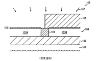
図1Aは基板101を備えた半導体デバイス100の断面図を模式的に示しており、基板101の上方には、その内部及びその上方に複数のトランジスタ要素を形成するために適切な厚みを有するシリコン含有半導体材質103が形成されている。図示される例では、例えば二酸化シリコン材質の形態にある埋め込み絶縁層102が基板101とシリコン含有半導体材質103の間に配置されている。また、第1の結晶性「能動(active)」領域103Aと第2の能動領域103Bを画定するように、浅い溝分離(shallow trench isolation)のような分離構造104が半導体層103内に形成されている。この関連において、能動領域は、1つ以上のトランジスタ要素に対してpn接合を形成するように適切なドーパントプロファイルがその内部に生成されることになる半導体材質として理解されるべきである。図示される例では、第1の能動領域103Aはpチャネルトランジスタに対応しているであろう一方、第2の能動領域103Bはnチャネルトランジスタに対応しているであろう。更に、例えば二酸化シリコン材質等の形態にあるマスク層105が、少なくとも第1及び第2の能動領域103A,103Bを覆うように形成されるであろう一方で、マスク層105を形成するためのプロセスに応じて分離構造104は露出させられているであろう。加えて、例えばレジストマスクの形態にあるエッチングマスク106が設けられており、エッチングマスク106は第2の能動領域103Bを覆うと共に第1の能動領域103Aは露出させる。
FIG. 1A schematically shows a cross-sectional view of a
図1Aに示される半導体デバイス100は、典型的には以下のプロセス技術に基いて形成され得る。先ず、分離構造104が十分に確立されたリソグラフィ、エッチング、堆積、平坦化、及び焼鈍の技術に基いて形成され、この場合、例えばリソグラフィプロセスに基いて半導体層103内に溝が形成され、その溝は次いで二酸化シリコン、シリコン窒化物等のような適切な絶縁材質で充填されることになる。過剰な材質を除去すると共に表面形状(surface topography)を平坦化した後、能動領域103A,103B内にその内部及びその上方に形成されるべきトランジスタのタイプに対応して基本ドーパント濃度を生成するための対応するドーパント種を導入するために、適切なマスクレジームを用いて活性注入シーケンス(active implantation sequences)を実行することによって、更なる処理が典型的には継続する。ドーパント種を活性化すると共に注入誘起損傷を再結晶化させた後、マスク層105を例えば酸化プロセス等に基いて形成することによって更なる処理が継続され得る。次いで、エッチングプロセス107の間に除去されるべきマスク層105の一部分を露出させるためにエッチングマスク106が形成され、エッチングプロセス107は、例えばマスク層105が二酸化シリコンから構成される場合にはフッ酸(HF)を用いるウエット化学的エッチングステップとして実行され得る。更に、エッチングマスク106を除去した後、後の製造段階において形成されることになる金属含有電極材質との組み合わせにおいてスレッショルド電圧又はバンドギャップエネルギを調節するために適切に設計されたシリコン/ゲルマニウム合金の選択的な堆積に対して第1の能動領域103Aを準備するために、露出された表面が処理され得る。
The
図1Bは選択的エピタキシャル成長プロセス108の間における半導体デバイス100を模式的に示しており、選択的エピタキシャル成長プロセス108においては、露出させられた能動領域103Aに対しては顕著な材質堆積が制限され得る一方で誘電体表面区域上の材質堆積は無視し得るように、十分に確立されたレシピに従ってプロセスパラメータが選択される。その結果、選択的エピタキシャル成長プロセス108の間、シリコン/ゲルマニウム合金109が選択的に能動領域103A上に形成され得るが、分離構造104上及びマスク層105上へのその堆積は抑制され得る。例えば洗練された応用においては、シリコン/ゲルマニウム合金109は概ね10nm以下の厚みで設けられるであろう一方で、ゲルマニウム濃度は概ね25原子パーセントであろう。シリコン/ゲルマニウム合金109の組成及びその厚みは、最終的に得られるスレッショルド電圧及びそれに伴い最終的に得られるトランジスタ特性に大きな影響を有し得ることが理解されるべきである。
FIG. 1B schematically illustrates the
図1Cは更に進んだ製造段階における半導体デバイス100を模式的に示している。図示されるように、デバイス100は例えばウエット化学的エッチング環境の形態にあるエッチング環境110に曝され、エッチング環境112においては、マスク層105(図1B参照)は、能動領域103Bの材質及び先に堆積させられたシリコン/ゲルマニウム合金109に対して選択的に除去される。例えば、エッチング環境110はフッ酸に基いて実行され、フッ酸は材質103B及び109に対して高度な選択性で二酸化シリコン材質を除去することができる。その後、更なる処理が継続されて、ゲート電極を形成すると共に基本的トランジスタ構造を完成することができる。
FIG. 1C schematically illustrates the
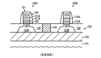
図1Dは進んだ製造段階における半導体デバイス100を模式的に示している。この段階においては、pチャネルトランジスタ150Aが能動領域103Aの内部及び上方に形成され、またnチャネルトランジスタ150Bが能動領域103Bの内部及び上方に形成される。トランジスタ150A,150Bは両方とも前述したように高k誘電体材質を備えたゲート絶縁層151Bを含む電極構造151を備えている。更に、アルミニウム酸化物、チタン窒化物等のような金属含有電極材質がゲート絶縁層151B上に形成されるであろうし、次いで多結晶シリコン151Cのような更なる電極材質が形成されるであろう。図示されるように、pチャネルトランジスタ150Aにおいては、トランジスタ150Aのスレッショルド電圧、即ち伝導性チャネルがチャネル領域153内に形成される電圧が、合金109並びに材質151B及び151Aの特性と、前述したように洗練されたドーパントプロファイルに基いて形成されるであろうドレイン及びソース領域154の対応する特性との組み合わせによって決定され得るように、ゲート絶縁層151Bがシリコン/ゲルマニウム合金109上に形成されている。一方、トランジスタ150Bのチャネル領域153のバンドギャップ構造は、結合材質151B,151Aに対して適切である。
FIG. 1D schematically illustrates the
トランジスタ150A,150Bは、ゲート絶縁層151B、電極材質151A及び多結晶シリコン材質151Cの堆積と洗練されたリソグラフィ及びエッチングの技術を用いるそれらのパターニングとを含む十分に確立された製造技術に基いて形成され得る。その後、ドレイン及びソース領域154に対する縦方向及び横方向のドーパントプロファイルを適切に画定するために、スペーサ構造152を形成するための製造シーケンスとの組み合わせにおいて、対応する注入シーケンスが実行され得る。ドーパントを活性化すると共に注入誘起損傷を再結晶化するための対応する焼鈍プロセスの後、必要であればドレイン及びソース領域154並びに多結晶シリコン材質151Cの内部に金属シリサイド領域(図示せず)を形成することによって、基本的トランジスタ構造が完成され得る。
pチャネルトランジスタ150Aのスレッショルド電圧は、シリコン/ゲルマニウム合金109を設けることによって効果的に調節することができるが、pチャネルトランジスタのスレッショルド電圧の大きなばらつきが観察されることがあり、特に密にパッキングされたデバイス領域及びデバイス区域(densely packed device regions and the device areas)におけるpチャネルトランジスタのスレッショルド電圧の著しい偏差が観察されることがある。従って、50nm以下のゲート長を有する高度に縮小化されたトランジスタ要素を必要とする洗練された応用に対しては、洗練された高k金属ゲート電極構造を備えたトランジスタのスレッショルド電圧を調節するための従来の戦略は、従来のプロセスフローにおいて生じる大きなスレッショルドばらつきに起因して、それほど望ましくはないであろう。
Although the threshold voltage of the p-
上述した状況に鑑み、本開示は、チャネル領域内に設けられる半導体合金に基いて効果的なスレッショルド調節が達成され得る一方で、上で特定した1つ以上の問題の影響を回避し又は少なくとも低減することができる製造技術及び半導体デバイスに関連している。 In view of the circumstances described above, the present disclosure avoids or at least reduces the effects of one or more of the problems identified above, while effective threshold adjustment can be achieved based on a semiconductor alloy provided in the channel region. It relates to manufacturing technology and semiconductor devices that can be made.
概して、本開示は、スレッショルド調節半導体材質の堆積の間におけるプロセス不均一性を低減することによって、スレッショルド調節半導体合金を含むトランジスタのスレッショルドばらつきを大幅に低減し得る半導体デバイス及び製造技術を提供する。この目的のために、スレッショルド調節半導体材質を堆積させるためのエピタキシャル成長プロセスの間における「パターンローディング(pattern loading)」の程度が減少させられてよく、それにより、個々の半導体ダイ及び全体的な基板にわたる高度な均一性を得ることができる。この点において、「パターンローディング」の用語は、対応する材質がその上に堆積させられることになる区域の「近隣(neighborhood)」に依存する堆積プロセスの間における層厚及び/又は材質組成のばらつきの影響として理解することができる。即ち、典型的には、堆積挙動は局所的な堆積条件に依存するであろうし、同時に堆積条件は堆積区域の近隣によって決定されるであろうし、この場合、特に密にパッキングされたデバイス領域と密でなくパッキングされたデバイス領域の間での顕著な差が観察されることがある。従って、ここに開示される原理に従うと、スレッショルド調節材質をより「グローバルな(global)」様態で堆積させると共に後続の均一で且つ十分に可制御なパターニングシーケンスでこれをパターニングすることによって、対応する局所的堆積条件はより均一になり得る。 In general, the present disclosure provides semiconductor devices and fabrication techniques that can significantly reduce threshold variations in transistors that include threshold-adjusted semiconductor alloys by reducing process non-uniformity during deposition of the threshold-adjusted semiconductor material. For this purpose, the degree of “pattern loading” during the epitaxial growth process for depositing the threshold control semiconductor material may be reduced, thereby extending across individual semiconductor dies and the entire substrate. A high degree of uniformity can be obtained. In this regard, the term “pattern loading” refers to variations in layer thickness and / or material composition during the deposition process that depend on the “neighborhood” of the area over which the corresponding material is to be deposited. Can be understood as the influence of That is, typically, the deposition behavior will depend on the local deposition conditions, and at the same time the deposition conditions will be determined by the neighborhood of the deposition area, in this case especially in the densely packed device region. Significant differences may be observed between non-dense and packed device regions. Thus, according to the principles disclosed herein, the threshold adjustment material is deposited in a more “global” manner and patterned by a subsequent uniform and sufficiently controllable patterning sequence. Local deposition conditions can be more uniform.
ここに開示される1つの例示的な方法は、第1のシリコン含有結晶性半導体領域及び第2のシリコン含有結晶性半導体領域上にシリコン含有半導体合金の層を形成することを備えている。方法はまた、第2のシリコン含有結晶性半導体領域からシリコン含有半導体合金の層を選択的に除去することを備えている。更に、方法は、第1のトランジスタの第1のゲート電極構造をシリコン含有半導体合金の層上に形成することを備えており、ここでは、第1のゲート電極構造は、高k誘電体ゲート絶縁層及び高k誘電体ゲート絶縁層上に形成される金属含有ゲート電極材質を備えている。最後に、方法は、第2のトランジスタの第2のゲート電極構造を第2のシリコン含有結晶性半導体領域の上方に形成することとを備えており、ここでは、第2のゲート電極構造は、高k誘電体ゲート絶縁層及びその上に形成される金属含有ゲート電極材質を備えている。 One exemplary method disclosed herein comprises forming a layer of a silicon-containing semiconductor alloy over a first silicon-containing crystalline semiconductor region and a second silicon-containing crystalline semiconductor region. The method also comprises selectively removing a layer of silicon-containing semiconductor alloy from the second silicon-containing crystalline semiconductor region. The method further comprises forming a first gate electrode structure of the first transistor on the layer of silicon-containing semiconductor alloy, wherein the first gate electrode structure is a high-k dielectric gate insulation. A metal-containing gate electrode material formed on the layer and the high-k dielectric gate insulating layer. Finally, the method comprises forming a second gate electrode structure of a second transistor over the second silicon-containing crystalline semiconductor region, wherein the second gate electrode structure comprises: A high-k dielectric gate insulating layer and a metal-containing gate electrode material formed thereon are provided.
ここに開示される更なる例示的な方法は、第1及び第2のシリコン含有半導体領域上にスレッショルド調節半導体材質を形成することを備えている。また、第1のシリコン含有半導体領域を覆う注入マスクを用いることによって、第2のシリコン含有半導体領域内にドーパント種が導入される。方法は更に、注入マスクに基いて第2のシリコン含有半導体領域から選択的にスレッショルド調節半導体材質を除去することを備えている。最後に、方法は、スレッショルド調節半導体材質上の第1のトランジスタの第1のゲート電極構造及び第2のシリコン含有半導体領域上の第2のトランジスタの第2のゲート電極構造を形成することとを備えており、第1及び第2のゲート電極構造は、高k誘電体材質と高k誘電体材質上に形成される金属含有電極材質とを備えている。 A further exemplary method disclosed herein comprises forming a threshold adjustment semiconductor material over the first and second silicon-containing semiconductor regions. Further, by using an implantation mask that covers the first silicon-containing semiconductor region, dopant species are introduced into the second silicon-containing semiconductor region. The method further comprises selectively removing the threshold adjustment semiconductor material from the second silicon-containing semiconductor region based on the implantation mask. Finally, the method includes forming a first gate electrode structure of the first transistor on the threshold adjusted semiconductor material and a second gate electrode structure of the second transistor on the second silicon-containing semiconductor region. The first and second gate electrode structures include a high-k dielectric material and a metal-containing electrode material formed on the high-k dielectric material.
ここに開示される1つの例示的な半導体デバイスは、概ね100ナノメートル以下のピッチを規定する複数の密にパッキングされた第1のpチャネルトランジスタを備えた第1のデバイス領域を備えている。第1のpチャネルトランジスタの各々は、第1のシリコン含有半導体領域の内部及び上方に形成されると共に、第1のpチャネルトランジスタの各々のチャネル領域内のスレッショルド調節半導体合金の第1の層を備えている、半導体デバイスは更に、100ナノメートルを超えるピッチを規定する複数の第2のpチャネルトランジスタを備えた第2のデバイス領域を備えており、第2のpチャネルトランジスタの各々は、第2のシリコン含有半導体領域の内部及び上方に形成されると共に、第2のpチャネルトランジスタの各々のチャネル領域内のスレッショルド調節半導体合金の第2の層を備えている。また、スレッショルド調節半導体合金の第1及び第2の層の材質組成及び/又は層厚の均一性の程度は、概ね±2パーセントである。 One exemplary semiconductor device disclosed herein comprises a first device region comprising a plurality of closely packed first p-channel transistors that define a pitch of approximately 100 nanometers or less. Each of the first p-channel transistors is formed within and above the first silicon-containing semiconductor region and includes a first layer of a threshold-adjusting semiconductor alloy in each channel region of the first p-channel transistor. The semiconductor device further comprises a second device region comprising a plurality of second p-channel transistors defining a pitch greater than 100 nanometers, each of the second p-channel transistors comprising: And a second layer of threshold-adjusting semiconductor alloy formed within and above the two silicon-containing semiconductor regions and in each channel region of the second p-channel transistor. The degree of uniformity of the material composition and / or layer thickness of the first and second layers of the threshold control semiconductor alloy is approximately ± 2%.
本開示の更なる実施形態は、添付の特許請求の範囲において画定されており、また添付の図面を参照したときに以下の詳細な説明と共に更に明らかになろう。 Further embodiments of the present disclosure are defined in the appended claims, and will become more apparent with the following detailed description when taken in conjunction with the accompanying drawings.
以下の詳細な説明及び図面に説明される実施形態を参照して本開示が説明されるが、以下の詳細な説明及び図面は、ここに開示される主題を特定の開示される例示的な実施形態に限定することを意図するものではない一方で、むしろ説明されている例示的な実施形態は、本開示の種々の側面を単に例示するものであり、本開示の範囲は添付の特許請求の範囲によって画定されていることが理解されるべきである。 The present disclosure will be described with reference to the following detailed description and the embodiments described in the drawings, but the following detailed description and the drawings illustrate specific disclosed exemplary implementations of the subject matter disclosed herein. While not intended to be limited to the forms, rather, the described exemplary embodiments are merely illustrative of various aspects of the disclosure, and the scope of the disclosure is defined by the appended claims. It should be understood that it is defined by a range.
概して、本開示は、高k誘電体材質及び金属含有電極構造に基き初期の製造段階において洗練されたゲート電極構造が形成され得る半導体デバイス及び技術を提供する。この場合、1つのタイプのトランジスタのスレッショルド電圧は、対応するトランジスタのチャネル領域内に適切な半導体材質を設けることによって調節することができ、このことは高い均一性の製造プロセスに基いて達成することができ、それにより、層厚及び/又は材質組成の概ね±5%程度の小さい偏差に基いてスレッショルドばらつきを低減することができる。即ち、半導体デバイス100を参照して既に説明したように、従来の製造戦略においては、対応する目標値に対して層厚及び/又はゲルマニウム濃度に関して概ね5%のばらつきでシリコン/ゲルマニウム合金を設けることは、顕著なスレッショルドばらつきをもたらし、このスレッショルドばらつきは、概ね50nm以下の臨界寸法に基いてトランジスタが形成されるであろう洗練された集積回路の要求に適合し得ないであろう。スレッショルド調節半導体合金を形成するための堆積プロセスの間におけるパターン関連の不均一性は、特に密にパッキングされたトランジスタ要素を含むデバイス区域及びそれほど臨界的ではないパッキング密度のデバイス区域に関して、結果として得られるスレッショルドばらつきに大きな影響を有するであろうことが認識されてきた。従って、幾つかの例示的な実施形態によると、スレッショルド調節半導体合金を形成するための臨界的なエピタキシャル堆積プロセスは、進歩した表面状態に基いて実行されてよく、つまり、半導体合金の均一性の程度が結果として高められ得るように、堆積表面区域及び非堆積区域に関して増大された程度の均一性で実行されてよい。この点において、均一性の程度は、対応するパラメータの所与の目標値の概ね3%の偏差として理解することができる。例えば、スレッショルド調節半導体材質の材質組成は、概ね3%以下で、即ち目標値と比較して±3%で変化してよく、目標値は多数の対応する材質サンプルから取られる平均値によって定義され得る。他の場合には、層厚は対応する目標厚みに対して概ね±3%以下で偏位してよい。
In general, the present disclosure provides semiconductor devices and techniques in which sophisticated gate electrode structures can be formed in early manufacturing stages based on high-k dielectric materials and metal-containing electrode structures. In this case, the threshold voltage of one type of transistor can be adjusted by providing an appropriate semiconductor material in the channel region of the corresponding transistor, which should be achieved based on a highly uniform manufacturing process. Accordingly, threshold variation can be reduced based on a small deviation of about ± 5% of the layer thickness and / or material composition. That is, as already described with reference to the
高められた程度の均一性は、幾つかの例示的な実施形態では、スレッショルド調節半導体合金を「非選択的な(non-selective)」様態で堆積させることによって達成することができ、ここでは、半導体合金は、任意のタイプのトランジスタの能動領域上に堆積させられてよく、そして十分に可制御なエッチングプロセスに基いてnチャネルトランジスタのような1つのタイプのトランジスタから次いで除去されてよい。「非選択的な」堆積という用語は、それにもかかわらず、ある程度の選択性が結晶性半導体表面と誘電体表面区域との間で達成され得る場合についても参照し得ることが理解されるべきであり、誘電体表面区域は分離構造等の形態で設けられるであろう。このように、半導体合金の堆積が結晶性半導体表面に限定されているであろう場合であっても、密にパッキングされたデバイス領域が考慮されているか密でなくパッキングされたデバイス領域が考慮されているかにかかわらず、典型的には両タイプのトランジスタは近接して配置されるであろうという理由で局所的スケールでは極めて類似した堆積条件が達成され得るので、全体的な半導体ダイ又は複数の半導体ダイを含む基板にわたって大幅に改善された堆積条件を達成することができる。他の例示的な実施形態においては、分離構造は半導体合金を高度に非選択的な様態で堆積させた後に形成することができ、それにより堆積条件の均一性を更に高めることができる。ここに開示される幾つかの例示的な実施形態では、半導体合金のパターニングは追加的なリソグラフィステップを必要とすることなしに達成され得るので、高度に効率的な全体的な製造フローを提供することができる。 An increased degree of uniformity can be achieved in some exemplary embodiments by depositing the threshold-adjusted semiconductor alloy in a “non-selective” manner, where: The semiconductor alloy may be deposited on the active area of any type of transistor and then removed from one type of transistor, such as an n-channel transistor, based on a fully controllable etching process. It should be understood that the term “non-selective” deposition may nevertheless refer to the case where some degree of selectivity can be achieved between the crystalline semiconductor surface and the dielectric surface area. Yes, the dielectric surface area would be provided in the form of an isolation structure or the like. Thus, even when semiconductor alloy deposition would be limited to crystalline semiconductor surfaces, densely packed device regions are considered or not densely packed device regions are considered. Regardless, typically, both types of transistors will be placed in close proximity, so very similar deposition conditions can be achieved on a local scale, so that the overall semiconductor die or multiple Significantly improved deposition conditions can be achieved across the substrate including the semiconductor die. In other exemplary embodiments, the isolation structure can be formed after the semiconductor alloy is deposited in a highly non-selective manner, thereby further enhancing the uniformity of the deposition conditions. In some exemplary embodiments disclosed herein, semiconductor alloy patterning can be achieved without the need for additional lithography steps, thus providing a highly efficient overall manufacturing flow. be able to.
図2A〜2Mを参照して更なる例示的な実施形態をより詳細に以下に説明し、必要である場合には図1A〜1Dが再び参照されることがある。 Further exemplary embodiments are described in more detail below with reference to FIGS. 2A-2M, and FIGS. 1A-1D may be referenced again if necessary.
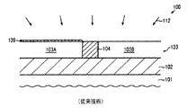
図2Aは基板201及びシリコン含有半導体層203を備えた半導体デバイス200の断面図を模式的に示している。また、幾つかの例示的な実施形態では、例えば図2Aに示されるように、デバイス200の少なくとも一部分はSOIアーキテクチャを備えていてよく、SOIアーキテクチャにおいては、埋め込み絶縁層202が基板201とシリコン含有半導体層203の間に配置されていてよい。しかし、ここに開示される原理は「バルク(bulk)」構造にも容易に適用することができ、バルク構造においては、少なくともデバイス200の幾つかの部分において埋め込み絶縁層202は除かれていてよいことが理解されるべきである。更に、半導体層203内には浅い溝分離(shallow trench isolation)のような分離構造204が設けられていてよく、それにより第1の能動領域203A及び第2の能動領域203Bが画定され得る。図示される実施形態においては、能動領域203A,203Bは、能動領域203A,203Bの内部及び上方に更に形成されることになる対応するトランジスタの伝導性タイプを規定するための基本的ドーピングを備えていてよい。1つの例示的な実施形態では、能動領域203Aはpチャネルトランジスタを形成するためにnドープ領域を代表してよい。同様に能動領域203Bは、nチャネルトランジスタの能動領域を代表してよい。以下、製造シーケンスが論じられ、その製造シーケンスにおいては、能動領域203A内に形成されることになるトランジスタのための対応するスレッショルド電圧をもたらすために、スレッショルド調節半導体合金が能動領域203A上に選択的に形成されてよい。一方、全体的なデバイス要求及びプロセス要求に応じて、スレッショルド電圧を調節するための対応するメカニズムはまた、能動領域203B内に形成されることになるトランジスタ又は両方のトランジスタに適用され得ることが理解されるべきである。
FIG. 2A schematically shows a cross-sectional view of a
また、これまでに説明された構成要素に関して、そしてそれらを形成するための製造技術に関して、半導体デバイス100を参照して既に説明されたのと同じ基準を適用し得る。図示される実施形態では、分離構造204を形成し、そして能動領域203A,203B内に基本的ドーピングを画定した後、デバイス200は、十分に確立されたウエット化学的レシピに基づいて実行され得る洗浄プロセス211にさらされてよい。例えば、先行する製造ステップの間に形成されたであろう任意の自然酸化物が除去され得る。
Also, the same criteria already described with reference to the
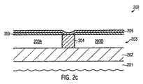
図2Bはエピタキシャル成長プロセス208の間における半導体デバイス200を模式的に示しており、エピタキシャル成長プロセス208においては、例えばシリコン/ゲルマニウム材質等の形態にある半導体合金209が、従来の戦略と比べて表面状態の高い均一性に基いて堆積され得る。即ち、1つの例示的な実施形態では、エピタキシャル成長プロセス208は、「選択的(selective)」堆積レシピのような十分に確立されたプロセスパラメータに基いて実行することができ、この場合、材質密着は実質的に領域203A,203Bのような露出させられた結晶性表面区域上で生じ得る一方で、分離構造204のような誘電体表面区域上での明白な材質堆積は抑制され得る。この意味において、プロセス208は選択的エピタキシャル成長プロセスと称されてよいが、半導体合金209は、能動領域203A,203Bに対して非選択的な様態で形成されてもよい。つまり、その上への材質209の堆積が従来どおり抑制される領域203Bのような1つ以上の更なるトランジスタ要素又は能動領域が領域203Aに極く接近して典型的には配置されるという理由で、対応するデバイス領域内の全体的なパッキング密度にかかわらず能動領域203Aの堆積に対する局所的近傍は類似しているであろうから、従来の手法とは対照的に、領域203A,203Bの表面区域のすぐ上での堆積速度及び/又は任意の前駆体の存在は、全体的な基板201においてさえも極めて類似しているであろう。従って、対応する「エッジ状態(edge conditions)」は、材質209の堆積が必要になるトランジスタタイプに対応する任意の能動領域に対して同様であり得る。その結果、材質209の厚み209Tは、高度な均一性を有することができ、また、全体的な基板201にわたってとり得る対応する代表的な平均値に対して概ね±3%以下で変化するであろう。他の例示的な実施形態においては、厚みばらつきは実に概ね2%以下であり得る。例えば、対応する金属含有電極材質との組み合わせにおいて設けられることになるダイオードバンドギャップオフセットに応じて、半導体合金209は、概ね10nm以下、例えば9nmの厚みを有するシリコン/ゲルマニウム合金を代表してよく、ゲルマニウム濃度は概ね25原子%以下であってよい。従って、堆積プロセス208の間におけるガス流量の高い均一性に起因して、材質組成のばらつきもまた強化され、即ち、用いられる半導体合金209のタイプに応じてシリコン、ゲルマニウム等の種々の成分の(変動の)割合は低減されるであろうし、また代表的な平均値又は目標値に対して概ね±3%以下の範囲内になり得る。
FIG. 2B schematically illustrates the
図2Cは更に進んだ製造段階における半導体デバイス200の断面図を模式的に示している。図示されるように、マスク層205が半導体合金209上に形成され、マスク層205は、二酸化シリコン、シリコン窒化物、等のような任意の適切な材質から構成され得る。幾つかの例示的な実施形態では、マスク層205は材質209の酸化物から形成されていてよく、従って対応する成分がマスク層205内でも得られる。層205は、プラズマ支援CVD(化学的気相堆積)、熱的に活性化されたCVD、等のような十分に確立された堆積技術に基いて形成することができる。他の場合には、酸化プロセス、例えば熱酸化、プラズマ支援酸化、ウエット化学的酸化、等が実行されてよく、この場合、対応する酸化プロセスの高度な可制御性が、初期層209の材質消費の正確な制御を可能にし得る。即ち、多数の酸化レシピに対する十分に知られ且つ安定な酸化速度により、材質消費の程度は予め決定され得るし、そして層209を堆積させるに際して適切な初期厚みと共に考慮に入れられ得る。対応する酸化プロセスの高度な均一性により、これらの酸化プロセスに基くマスク層205の酸化は、付加的な全体的プロセス不均一性の一因には実質上ならないであろう。
FIG. 2C schematically shows a cross-sectional view of the
図2Dはある製造段階における半導体デバイス200を模式的に示しており、その製造段階においては、能動領域203A並びにその上に形成された対応する材質層209及び205を覆う一方で、能動領域203B及びその上に形成される対応する材質を、少なくともマスク層205の材質を除去するように設計されるエッチング環境207に曝すように、マスク206が設けられてよい。図示される実施形態においては、エッチングプロセス207は、材質209に対して材質205を選択的に除去するように実行されてよく、このことは、マスク層205が二酸化シリコンから構成される場合には、例えばフッ酸に基いて達成され得る。他の場合には、層205の露出させられた部分を選択的に除去するために、任意の他の選択的エッチングレシピが用いられてよい。
FIG. 2D schematically illustrates the
図2Eは更なるエッチング環境212に曝されるときの半導体デバイス200を模式的に示しており、エッチング環境212は、少なくともマスク層205に対して層209の材質を選択的に除去するための適切なエッチング薬品に基いて確立され得る。1つの例示的な実施形態では、エッチング環境212は、二酸化シリコン、シリコン窒化物等から構成され得るマスク層205に対して選択的なシリコン/ゲルマニウム合金のような材質209の除去を可能にする化学薬品に基くウエット化学的エッチングプロセスとして実行されてよい。エッチングプロセス212の間、化学薬品の濃度、プロセス時間等のようなパラメータが、能動領域203Bの材質を過度に消費しないように適切に選択されてよい。1つの例示的な実施形態では、エッチングプロセス212はテトラメチルアンモニウムヒロドキシド(TMAH)に基いて実行されてよく、TMAHはレジスト材質を除去するためのよく知られた薬品であるが、高濃度且つ高温ではシリコンベースの材質を効果的に除去することもできる。更に、TMAHはまた、二酸化シリコン及びシリコン窒化物材質に対して明白な選択性を呈し得る。従って、レジストマスク206(図2D参照)がエッチングプロセス212の間に除去されるであろうとしても、能動領域203Aの上方の材質層209の完全性を損なうことなしに、高度な可制御性で層209を除去することができる。他の場合には、全体的なプロセス均一性を更に高めるために、エッチングプロセス212を開始するのに先立ちレジストマスクが除去されてよい。その結果、能動領域203Bを露出させるためのパターニングシーケンスの間における材質209の全体的な完全性は、マスク層205によって維持され得る。その後、マスク層205は能動領域203Aの上方から除去されてよく、ここでは、エッチングプロセス110(図1C)を参照したときの半導体デバイス100に関して既に説明したのと同様なプロセス技術を適用することができる。半導体合金209を露出させた後、前述したように洗練されたゲート電極構造を形成するために、十分に確立されたプロセス技術に基いて更なる処理が継続されてよい。
FIG. 2E schematically illustrates the
図2Fは更なる例示的な実施形態に従う半導体デバイス200を模式的に示しており、その実施形態においては、分離構造を形成するのに先立ち、領域203A,203Bのための基本的なドーピングが既に確立されていてよい。また、任意の適切な堆積レシピに基いて半導体合金209を形成するために、デバイス200はエピタキシャル成長プロセス208に曝されてよく、ここでは、分離構造がないことに起因して、更に強化された程度の堆積条件が達成され得る。その結果、この場合にもまた、前述したように、材質組成及び層厚に関する高度な均一性で材質209を設けることができる。半導体合金209を形成した後、層209をパターニングすると共に分離構造を形成することによって更なる処理が継続されてよく、ここでは、高められたプロセス均一性を維持するための適切な製造戦略は、図2Lを参照して後で説明される。
FIG. 2F schematically illustrates a
図2G〜2Jを参照して更なる例示的な実施形態が以下に説明されることになり、その実施形態においては、一方の能動領域内の基本的なドーパント濃度を規定するために用いられる注入マスクに基いて、スレッショルド調節半導体合金のパターニングが達成され得る。 A further exemplary embodiment will be described below with reference to FIGS. 2G-2J, in which the implant used to define the basic dopant concentration in one active region. Based on the mask, patterning of the threshold adjusted semiconductor alloy can be achieved.
図2Gはある製造段階における半導体デバイス200を模式的に示しており、1つの例示的な実施形態では、能動領域203A,203Bを分離するように分離構造204が形成されてよいが、対応する基本的ドーピングレベルは未だ確立されていなくてよい。他の例示的な実施形態においては、分離構造204はこの製造段階では破線によって示されるようには形成されなくてよく、そして図2Fを参照して既に説明されたように、また図2Lを参照して更に詳細に説明されもするように、分離構造204は後の製造段階において形成されてよい。更に、デバイス200は、既に説明したように、半導体合金209を優れた均一性で形成するために、プロセス208の堆積環境に曝される。この製造段階において分離構造204が既に存在している場合には、半導体合金209は分離構造204の上方に形成されなくてよいことが理解されるべきである。
FIG. 2G schematically illustrates a
図2Hは更に進んだ製造段階における半導体デバイス200を模式的に示している。図示されるように、マスク層205が半導体合金209上に形成されてよく、ここでは、マスク層205は前述したような任意の適切な材質から構成されていてよい。また、能動領域203Aを曝す、即ちその上に形成されるマスク層205を露出させる一方で、能動領域203Bを覆うように、注入マスク214Aがレジストマスクの形態で設けられてよい。更に、デバイス200は、能動領域203A内へドーパント種を導入するように設計されたイオン注入プロセス213Aを受け、このことは十分に確立された注入レシピに基いて達成され得るが、注入エネルギ等のような対応するプロセスパラメータは、半導体合金209及びマスク層205の存在に対して適切に調節されてよい。しかし、両材質層は典型的には適度に小さい層厚で設けられているであろうから、従来の戦略に基いて対応する適合を容易に達成することができる。
FIG. 2H schematically illustrates the
図2Iは更に進んだ製造段階における半導体デバイス200を模式的に示しており、その製造段階においては、注入マスク214A(図2H参照)の除去の後、更なる注入マスク214Bが能動領域203Bを曝す、即ちその上に形成される材質層205,209を露出させてよい一方で、能動領域203Aの上方に形成される対応する材質層を覆ってよい。また、全体的なデバイス要求に従って能動領域203B内へドーパント種を導入するために、注入プロセス213Bが実行されてよい。
FIG. 2I schematically illustrates the
図2Jはエッチング環境207に曝されるときの半導体デバイス200を模式的に示しており、エッチング環境207は、例えば、マスク層205が注入マスク214Bに基いてパターニングされ得るウエット化学的エッチング環境の形態で提供される。従って、マスク層205をパターニングするための任意の追加的なリソグラフィステップが回避され得るので、極めて効率的な全体的プロセスフローに寄与することができる。
FIG. 2J schematically illustrates the
図2Kはマスク層205に基き半導体合金209の露出された部分を能動領域203Bの上方から除去するためのエッチング環境212に曝されるときの半導体デバイス200を模式的に示している。エッチングプロセス212のための任意のプロセスレシピに関して、前述したのと同じ基準を適用し得る。この場合にもまた、任意の追加的なリソグラフィステップを必要とすることなしに、高度に効率的な製造フローに基いて高度な均一性で半導体合金209を設けることができる。エッチングプロセス212の後、前述したように更なる処理が継続してよく、即ち、マスク層205が除去されてよく、そしてトランジスタ要素150A,150B(図1D参照)を参照して既に説明したように、洗練されたゲート電極構造を形成することによって更なる処理が継続してよい。
FIG. 2K schematically illustrates the
図2Lは更なる例示的な実施形態に従う半導体デバイス200を模式的に示しており、その実施形態においては、半導体合金209をパターニングした後に分離構造204が形成されてよい。例えば、図2G〜図2Kを参照して上述したプロセスシーケンスにおいては、分離構造を形成するのに先立ち注入マスクに基いて半導体合金209がパターニングされてよい一方で、他の場合には、図2Fを参照して説明されているように、領域203A,203B内の基本的なドーパント濃度を形成した後で半導体合金209がパターニングされてよい。いずれの場合においても、半導体合金209及びマスク層205の残りの部分に基いて更なる処理が継続してよく、これらは、材質209の完全性を高め、分離構造204を提供するための製造シーケンスの間に存在し得る任意のプロセス不均一性を低減するように維持されてよい。1つの例示的な実施形態では、図2Lに示されるように、停止層215、即ち任意の適切な堆積レシピに基いて堆積させられ得るシリコン窒化物材質のようなエッチング停止材質及び/又はCMP(化学的機械的研磨)停止材質が形成されてよい。全体的なプロセス戦略に応じて、必要であればデバイス200の表面形状が平坦化されてよく、他の場合には、更なる表面処理なしに層215に基いて更なる処理が継続してよい。従って、層215は、更なる処理のためのプラットフォーム、つまりエッチングマスクを画定すると共に半導体層203内へ溝をエッチングするためのシーケンス及び十分に確立された堆積レシピに基いてこれを充填することのためのプラットフォームとして用いられ得る。その後、任意の過剰な材質が例えばCMPによって除去されてよく、ここでは層215は停止層として機能する。その後、層215の残留物は除去されてよく、ここではマスク層205は依然として半導体合金209の完全性を維持し得る。その後、例えば前述したような任意のプロセス技術に基いてマスク層205は除去されてよく、次いで更なる処理が継続させられて洗練されたゲート電極構造が形成されてよい。
FIG. 2L schematically illustrates a
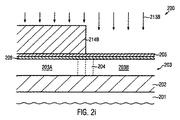
図2Mは進んだ製造段階における半導体デバイス200を模式的に示している。図示されるように、デバイス200は、pチャネルトランジスタのような複数の第1のトランジスタ250Aと1つ以上のnチャネルトランジスタ250Bとを含む第1のデバイス領域270Aを備えていてよい。更に、第2のデバイス領域270Bが設けられていてよく、第2のデバイス領域270B内には、pチャネルトランジスタのような複数の第3のトランジスタ250Cが場合によっては1つ以上のnチャネルトランジスタ(図示せず)と組み合わされて設けられていてよい。図示される実施形態においては、トランジスタ250A,250Cは、既に論じられたように所望のトランジスタ特性を提供するためにスレッショルド調節半導体合金209がその内部に形成された洗練されたトランジスタ要素を代表し得る。一方、トランジスタ250Bは、半導体合金に基く対応するスレッショルド調節が不要であってよいトランジスタを代表し得る。トランジスタ250A,250B及び250Cは各々ゲート電極構造251を備えていてよく、ゲート電極構造251は、前述したように高k誘電体材質に基いて形成されるゲート絶縁層251Bを備えていてよい。また、アルミニウム酸化物、チタン窒化物等のような金属含有電極材質251Aが、対応するゲート絶縁層251B上に形成されてよく、ここでは、必要であれば、多結晶シリコン材質等251Cのような追加的な電極材質が電極材質251A上に形成されてよい。更に、これも前述したように、所望の全体的なトランジスタ特性を得るために、洗練されたドレイン及びソース領域254が設けられてよい。
FIG. 2M schematically illustrates the
トランジスタ250A,250B及び250Cは、例えば既に論じられたような任意の適切な製造戦略に基いて形成することができ、ここでは、トランジスタ250A,250Cの各々内の半導体合金209の強化された均一性は、結果として得られるトランジスタ特性の優れた均一性を提供することができる。例えばデバイス270Aにおいては、隣接するトランジスタ250A間の距離又はピッチ250Pは、所望の高いパッキング密度を得るために最小臨界距離に対応していてよい。例えば洗練された応用においては、ピッチ250Pは概ね100nm以下であってよい一方、ゲート長、即ち図2Mにおける電極材質251Aの水平方向の拡張は概ね50nm以下であってよい。一方、隣接するトランジスタ250C間の対応する距離又はピッチは、全体的なデバイス要求に応じて大幅に大きくてよいにもかかわらず、対応する半導体合金209の強化された程度の均一性が、対応する距離250P,250Qとは関係なく、トランジスタばらつきの低減をもたらすことができる。既に説明したように、このことは半導体合金209の堆積の間に強化されるプロセス条件に基いて達成することができ、その理由は、局所的な意味においては、トランジスタ250C,250Aの各々に対する極めて類似した近隣(neighborhood)が達成され得るところにある。例えば、トランジスタ250Bはトランジスタ250A,250Cのそれぞれに対する「次の(next)」近隣を代表することができ、それにより、前述したように、材質209を形成する堆積プロセスの間に類似の局所的近隣を提供することができる。
結果として、本開示は半導体デバイス及び製造技術を提供し、本開示においては、スレッショルド調節半導体合金を形成することに対する堆積関連の不均一性は、各タイプのトランジスタのための能動領域上に当該材質を堆積させると共に次いで高度に可制御なパターニングシーケンスに基いて当該半導体合金をパターニングすることによって、低減され得る。その結果、シリコン/ゲルマニウム材質のようなスレッショルド調節半導体合金に基いて、早い製造段階において、即ちドレイン及びソース領域を形成するのに先立ち、高k誘電体材質及び金属含有電極材質を含む洗練されたゲート電極構造を形成することができ、ここでは、極度に縮小化された半導体デバイスが考慮されているとしても、スレッショルド調節材質の選択的な形成の間における強化された均一性が、スレッショルドばらつきの低減をもたらすことができる。 As a result, the present disclosure provides semiconductor devices and manufacturing techniques, in which the deposition related non-uniformities for forming the threshold-adjusted semiconductor alloy are reduced by the material on the active region for each type of transistor. And then patterning the semiconductor alloy based on a highly controllable patterning sequence. As a result, based on a threshold controlled semiconductor alloy such as a silicon / germanium material, it is refined to include a high-k dielectric material and a metal-containing electrode material at an early manufacturing stage, ie, prior to forming the drain and source regions. A gate electrode structure can be formed, where enhanced uniformity during selective formation of the threshold adjustment material, even when extremely miniaturized semiconductor devices are considered, A reduction can be brought about.
この明細書を考慮することで本開示の更なる修正及び変形が当業者には明らかであろう。従って、この明細書は、例示的なものとしてのみ解釈されるべきであり、そしてここに提供されている教示を実施する一般的な様態を当業者に教示することを目的とするものである。ここに示されそして説明される主題の形態は、目下のところ望ましい実施形態として受け止められるべきであるとして理解されるべきである。 Further modifications and variations of this disclosure will be apparent to those skilled in the art in view of this specification. Accordingly, this description is to be construed as illustrative only and is for the purpose of teaching those skilled in the art the general manner of carrying out the teaching provided herein. It should be understood that the form of the subject matter shown and described herein is to be taken as the presently preferred embodiment.
Claims (18)
前記第2のシリコン含有結晶性半導体領域から前記シリコン含有半導体合金の層を選択的に除去することと、
第1のトランジスタの第1のゲート電極構造であって、高k誘電体ゲート絶縁層及び前記高k誘電体ゲート絶縁層上に形成される金属含有ゲート電極材質を備えている第1のゲート電極構造を前記シリコン含有半導体合金の層上に形成することと、
第2のトランジスタの第2のゲート電極構造であって、高k誘電体ゲート絶縁層及び第2のゲート電極構造の前記高k誘電体ゲート絶縁層上に形成される金属含有ゲート電極材質を備えている第2のゲート電極構造を前記第2のシリコン含有結晶性半導体領域の上方に形成することと、
前記第1及び第2のトランジスタのドレイン及びソース領域の各々を、前記第1及び第2のシリコン含有結晶性半導体領域の各々に形成することと、を備え、
前記シリコン含有半導体合金の層を形成した後に前記第1のシリコン含有結晶性半導体領域内に第1のドーパント種を導入すると共に前記第2のシリコン含有結晶性半導体領域内に第2のドーパント種を導入することと、
前記第1及び第2のドーパント種を導入するのに先立ち前記シリコン含有半導体合金の層の上方にマスク層を形成することと、
前記第1のドーパント種を導入するために用いられる注入マスクを通じて前記マスク層をエッチングすることによって、前記第2のシリコン含有結晶性半導体領域の上方から前記マスク層を除去することと、を更に備えた方法。 Forming a layer of a silicon-containing semiconductor alloy on the first silicon-containing crystalline semiconductor region and the second silicon-containing crystalline semiconductor region;
Selectively removing the layer of the silicon-containing semiconductor alloy from the second silicon-containing crystalline semiconductor region;
A first gate electrode structure of a first transistor comprising a high-k dielectric gate insulating layer and a metal-containing gate electrode material formed on the high-k dielectric gate insulating layer Forming a structure on the silicon-containing semiconductor alloy layer;
A second gate electrode structure of a second transistor, comprising a high-k dielectric gate insulating layer and a metal-containing gate electrode material formed on the high-k dielectric gate insulating layer of the second gate electrode structure. Forming a second gate electrode structure overlying the second silicon-containing crystalline semiconductor region;
Forming each of the drain and source regions of the first and second transistors in each of the first and second silicon-containing crystalline semiconductor regions ,
After forming the silicon-containing semiconductor alloy layer, a first dopant species is introduced into the first silicon-containing crystalline semiconductor region and a second dopant species is introduced into the second silicon-containing crystalline semiconductor region. Introducing it,
Forming a mask layer above the layer of silicon-containing semiconductor alloy prior to introducing the first and second dopant species;
Removing the mask layer from above the second silicon-containing crystalline semiconductor region by etching the mask layer through an implantation mask used to introduce the first dopant species. method.
前記第1のシリコン含有半導体領域を覆う注入マスクを用いることによって、前記第2のシリコン含有半導体領域内にドーパント種を導入することと、
前記注入マスクを通じて前記スレッショルド調節半導体材質をエッチングすることによって、前記第2のシリコン含有半導体領域から選択的に前記スレッショルド調節半導体材質を除去することと、
前記スレッショルド調節半導体材質上の第1のトランジスタの第1のゲート電極構造及び前記第2のシリコン含有半導体領域上の第2のトランジスタの第2のゲート電極構造を形成することと、
前記第1及び第2のトランジスタのドレイン及びソース領域の各々を、前記第1及び第2のシリコン含有結晶性半導体領域の各々に形成することと、を備えた方法であって、
前記第1及び第2のゲート電極構造は高k誘電体材質と前記高k誘電体材質上に形成される金属含有電極材質とを備えている方法。 Forming a threshold adjusting semiconductor material on the first and second silicon-containing semiconductor regions;
Introducing a dopant species into the second silicon-containing semiconductor region by using an implantation mask covering the first silicon-containing semiconductor region;
Selectively removing the threshold adjustment semiconductor material from the second silicon-containing semiconductor region by etching the threshold adjustment semiconductor material through the implantation mask;
Forming a first gate electrode structure of a first transistor on the threshold-adjusting semiconductor material and a second gate electrode structure of a second transistor on the second silicon-containing semiconductor region;
Forming each of the drain and source regions of the first and second transistors in each of the first and second silicon-containing crystalline semiconductor regions, comprising:
The method wherein the first and second gate electrode structures comprise a high-k dielectric material and a metal-containing electrode material formed on the high-k dielectric material.
Applications Claiming Priority (5)
| Application Number | Priority Date | Filing Date | Title |
|---|---|---|---|
| DE102008063402A DE102008063402B4 (en) | 2008-12-31 | 2008-12-31 | Reducing the threshold voltage fluctuation in transistors with a channel semiconductor alloy by reducing the deposition nonuniformities |
| DE102008063402.6 | 2008-12-31 | ||
| US12/637,112 US8236654B2 (en) | 2008-12-31 | 2009-12-14 | Reduction of threshold voltage variation in transistors comprising a channel semiconductor alloy by reducing deposition non-uniformities |
| US12/637,112 | 2009-12-14 | ||
| PCT/EP2009/009307 WO2010076018A1 (en) | 2008-12-31 | 2009-12-29 | Reduction of threshold voltage variation in transistors comprising a channel semiconductor alloy by reducing deposition non-uniformities |
Publications (3)
| Publication Number | Publication Date |
|---|---|
| JP2012514318A JP2012514318A (en) | 2012-06-21 |
| JP2012514318A5 JP2012514318A5 (en) | 2013-02-07 |
| JP5669752B2 true JP5669752B2 (en) | 2015-02-18 |
Family
ID=42234616
Family Applications (1)
| Application Number | Title | Priority Date | Filing Date |
|---|---|---|---|
| JP2011542725A Active JP5669752B2 (en) | 2008-12-31 | 2009-12-29 | Reducing threshold voltage variation by reducing deposition non-uniformity in transistors with channel semiconductor alloys |
Country Status (6)
| Country | Link |
|---|---|
| US (1) | US8236654B2 (en) |
| JP (1) | JP5669752B2 (en) |
| KR (1) | KR101539416B1 (en) |
| CN (1) | CN102341906B (en) |
| DE (1) | DE102008063402B4 (en) |
| WO (1) | WO2010076018A1 (en) |
Families Citing this family (8)
| Publication number | Priority date | Publication date | Assignee | Title |
|---|---|---|---|---|
| DE102009006886B4 (en) | 2009-01-30 | 2012-12-06 | Advanced Micro Devices, Inc. | Reducing thickness variations of a threshold adjusting semiconductor alloy by reducing the patterning non-uniformities before depositing the semiconductor alloy |
| JP5605134B2 (en) * | 2010-09-30 | 2014-10-15 | 富士通セミコンダクター株式会社 | Semiconductor device and manufacturing method thereof |
| DE102010063296B4 (en) * | 2010-12-16 | 2012-08-16 | Globalfoundries Dresden Module One Limited Liability Company & Co. Kg | Production method with reduced STI topography for semiconductor devices with a channel semiconductor alloy |
| US8609509B2 (en) | 2011-09-22 | 2013-12-17 | Globalfoundries Inc. | Superior integrity of high-k metal gate stacks by forming STI regions after gate metals |
| US8377773B1 (en) * | 2011-10-31 | 2013-02-19 | Globalfoundries Inc. | Transistors having a channel semiconductor alloy formed in an early process stage based on a hard mask |
| US8541281B1 (en) | 2012-08-17 | 2013-09-24 | Globalfoundries Inc. | Replacement gate process flow for highly scaled semiconductor devices |
| US8969190B2 (en) | 2012-08-24 | 2015-03-03 | Globalfoundries Inc. | Methods of forming a layer of silicon on a layer of silicon/germanium |
| US9029919B2 (en) | 2013-02-01 | 2015-05-12 | Globalfoundries Inc. | Methods of forming silicon/germanium protection layer above source/drain regions of a transistor and a device having such a protection layer |
Family Cites Families (33)
| Publication number | Priority date | Publication date | Assignee | Title |
|---|---|---|---|---|
| DE69609313T2 (en) * | 1995-12-15 | 2001-02-01 | Koninkl Philips Electronics Nv | SEMICONDUCTOR FIELD EFFECT ARRANGEMENT WITH A SIGE LAYER |
| JP2000353753A (en) * | 1999-06-14 | 2000-12-19 | Hitachi Ltd | Manufacture of semiconductor device |
| JP4866534B2 (en) * | 2001-02-12 | 2012-02-01 | エーエスエム アメリカ インコーポレイテッド | Improved deposition method for semiconductor films. |
| WO2002082514A1 (en) * | 2001-04-04 | 2002-10-17 | Massachusetts Institute Of Technology | A method for semiconductor device fabrication |
| JP2004006959A (en) * | 2001-04-12 | 2004-01-08 | Matsushita Electric Ind Co Ltd | Semiconductor device and manufacturing method thereof |
| US6794252B2 (en) * | 2001-09-28 | 2004-09-21 | Texas Instruments Incorporated | Method and system for forming dual work function gate electrodes in a semiconductor device |
| US6600170B1 (en) * | 2001-12-17 | 2003-07-29 | Advanced Micro Devices, Inc. | CMOS with strained silicon channel NMOS and silicon germanium channel PMOS |
| AU2002357376A1 (en) * | 2002-03-28 | 2003-10-13 | Advanced Micro Devices, Inc. | Semiconductor device having a retrograde dopant profile in a channel region and method for fabricating the same |
| KR100487525B1 (en) * | 2002-04-25 | 2005-05-03 | 삼성전자주식회사 | Semiconductor device using silicon-germanium gate and method for fabricating the same |
| JP2003332458A (en) * | 2002-05-09 | 2003-11-21 | Fujitsu Ltd | Semiconductor device and its manufacturing method |
| KR20030090411A (en) * | 2002-05-23 | 2003-11-28 | 삼성전자주식회사 | CMOS gate electrode using selective growth and fabrication method the same |
| WO2004061944A1 (en) * | 2003-01-07 | 2004-07-22 | S.O.I.Tec Silicon On Insulator Technologies | Recycling of a wafer comprising a multi-layer structure after taking-off a thin layer |
| US6828181B2 (en) * | 2003-05-08 | 2004-12-07 | International Business Machines Corporation | Dual gate material process for CMOS technologies |
| JP4322255B2 (en) * | 2003-08-05 | 2009-08-26 | 富士通マイクロエレクトロニクス株式会社 | Semiconductor device and manufacturing method thereof |
| US7223679B2 (en) * | 2003-12-24 | 2007-05-29 | Intel Corporation | Transistor gate electrode having conductor material layer |
| JPWO2005106949A1 (en) * | 2004-04-30 | 2008-03-21 | 松下電器産業株式会社 | Semiconductor manufacturing method and semiconductor device |
| KR101292435B1 (en) * | 2004-09-14 | 2013-07-31 | 아리조나 보드 오브 리전트스, 아리조나주의 아리조나 주립대 대행법인 | Method for growing si-ge semiconductor materials and devices on substrates |
| JP2006108251A (en) * | 2004-10-01 | 2006-04-20 | Rohm Co Ltd | Manufacturing method of semiconductor device |
| JP2006202928A (en) * | 2005-01-19 | 2006-08-03 | Nec Electronics Corp | Method of manufacturing semiconductor device |
| US7132322B1 (en) * | 2005-05-11 | 2006-11-07 | International Business Machines Corporation | Method for forming a SiGe or SiGeC gate selectively in a complementary MIS/MOS FET device |
| TWI267926B (en) * | 2005-09-23 | 2006-12-01 | Ind Tech Res Inst | A new method for high mobility enhancement strained channel CMOS with single workfunction metal-gate |
| JP4795817B2 (en) * | 2006-03-02 | 2011-10-19 | 富士通セミコンダクター株式会社 | Manufacturing method of semiconductor device |
| JP2006332687A (en) * | 2006-07-10 | 2006-12-07 | Fujitsu Ltd | Cmos semiconductor device |
| KR100809327B1 (en) * | 2006-08-10 | 2008-03-05 | 삼성전자주식회사 | Semiconductor device and Method for fabricating the same |
| US7750374B2 (en) * | 2006-11-14 | 2010-07-06 | Freescale Semiconductor, Inc | Process for forming an electronic device including a transistor having a metal gate electrode |
| KR100773359B1 (en) * | 2006-11-20 | 2007-11-05 | 삼성전자주식회사 | Fabrication method of transistors having a high mobility and transistors fabricated thereby |
| US7598142B2 (en) * | 2007-03-15 | 2009-10-06 | Pushkar Ranade | CMOS device with dual-epi channels and self-aligned contacts |
| JP4898517B2 (en) * | 2007-03-27 | 2012-03-14 | シャープ株式会社 | Manufacturing method of semiconductor device |
| US7709331B2 (en) * | 2007-09-07 | 2010-05-04 | Freescale Semiconductor, Inc. | Dual gate oxide device integration |
| US7718496B2 (en) * | 2007-10-30 | 2010-05-18 | International Business Machines Corporation | Techniques for enabling multiple Vt devices using high-K metal gate stacks |
| US20090108294A1 (en) * | 2007-10-30 | 2009-04-30 | International Business Machines Corporation | Scalable high-k dielectric gate stack |
| US8053306B2 (en) * | 2007-12-13 | 2011-11-08 | International Business Machines Corporation | PFET with tailored dielectric and related methods and integrated circuit |
| JP2010157570A (en) * | 2008-12-26 | 2010-07-15 | Toshiba Corp | Method of manufacturing semiconductor device |
-
2008
- 2008-12-31 DE DE102008063402A patent/DE102008063402B4/en active Active
-
2009
- 2009-12-14 US US12/637,112 patent/US8236654B2/en active Active
- 2009-12-29 WO PCT/EP2009/009307 patent/WO2010076018A1/en active Application Filing
- 2009-12-29 CN CN200980157723.XA patent/CN102341906B/en active Active
- 2009-12-29 JP JP2011542725A patent/JP5669752B2/en active Active
- 2009-12-29 KR KR1020117018048A patent/KR101539416B1/en not_active IP Right Cessation
Also Published As
| Publication number | Publication date |
|---|---|
| JP2012514318A (en) | 2012-06-21 |
| WO2010076018A1 (en) | 2010-07-08 |
| KR101539416B1 (en) | 2015-07-27 |
| CN102341906A (en) | 2012-02-01 |
| US20100164014A1 (en) | 2010-07-01 |
| CN102341906B (en) | 2014-10-15 |
| US8236654B2 (en) | 2012-08-07 |
| DE102008063402A1 (en) | 2010-07-08 |
| DE102008063402B4 (en) | 2013-10-17 |
| KR20120067973A (en) | 2012-06-26 |
Similar Documents
| Publication | Publication Date | Title |
|---|---|---|
| JP5781944B2 (en) | Reducing semiconductor alloy thickness variations by reducing patterning non-uniformities prior to depositing a threshold controlled semiconductor alloy | |
| TWI438867B (en) | A cmos device having gate insulation layers of different type and thickness and a method of forming the same | |
| US8367495B2 (en) | Method for forming CMOS transistors having metal-containing gate electrodes formed on a high-K gate dielectric material | |
| US8343837B2 (en) | Work function adjustment in a high-k gate electrode structure after transistor fabrication by using lanthanum | |
| US8329549B2 (en) | Enhancing integrity of a high-k gate stack by protecting a liner at the gate bottom during gate head exposure | |
| JP5669752B2 (en) | Reducing threshold voltage variation by reducing deposition non-uniformity in transistors with channel semiconductor alloys | |
| US8378432B2 (en) | Maintaining integrity of a high-K gate stack by an offset spacer used to determine an offset of a strain-inducing semiconductor alloy | |
| US7981740B2 (en) | Enhanced cap layer integrity in a high-K metal gate stack by using a hard mask for offset spacer patterning | |
| US8119461B2 (en) | Reducing the creation of charge traps at gate dielectrics in MOS transistors by performing a hydrogen treatment | |
| US8349694B2 (en) | Enhanced confinement of high-K metal gate electrode structures by reducing material erosion of a dielectric cap layer upon forming a strain-inducing semiconductor alloy | |
| US8951901B2 (en) | Superior integrity of a high-K gate stack by forming a controlled undercut on the basis of a wet chemistry | |
| US8835209B2 (en) | Complementary transistors comprising high-k metal gate electrode structures and epitaxially formed semiconductor materials in the drain and source areas | |
| US20110027952A1 (en) | Formation of a channel semiconductor alloy by depositing a hard mask for the selective epitaxial growth | |
| US8524591B2 (en) | Maintaining integrity of a high-K gate stack by passivation using an oxygen plasma | |
| US20130115773A1 (en) | Prevention of ILD Loss in Replacement Gate Technologies by Surface Treatmen | |
| US8324091B2 (en) | Enhancing integrity of a high-k gate stack by confining a metal cap layer after deposition | |
| US8513080B2 (en) | Reducing contamination in a process flow of forming a channel semiconductor alloy in a semiconductor device | |
| US8377773B1 (en) | Transistors having a channel semiconductor alloy formed in an early process stage based on a hard mask | |
| WO2010086152A1 (en) | Reduction of thickness variations of a threshold adjusting semiconductor alloy by reducing patterning non-uniformities prior to depositing the semiconductor alloy |
Legal Events
| Date | Code | Title | Description |
|---|---|---|---|
| A521 | Request for written amendment filed |
Free format text: JAPANESE INTERMEDIATE CODE: A523 Effective date: 20121212 |
|
| A621 | Written request for application examination |
Free format text: JAPANESE INTERMEDIATE CODE: A621 Effective date: 20121212 |
|
| A131 | Notification of reasons for refusal |
Free format text: JAPANESE INTERMEDIATE CODE: A131 Effective date: 20140226 |
|
| A977 | Report on retrieval |
Free format text: JAPANESE INTERMEDIATE CODE: A971007 Effective date: 20140228 |
|
| A521 | Request for written amendment filed |
Free format text: JAPANESE INTERMEDIATE CODE: A523 Effective date: 20140526 |
|
| A131 | Notification of reasons for refusal |
Free format text: JAPANESE INTERMEDIATE CODE: A131 Effective date: 20140813 |
|
| A521 | Request for written amendment filed |
Free format text: JAPANESE INTERMEDIATE CODE: A523 Effective date: 20141105 |
|
| TRDD | Decision of grant or rejection written | ||
| A01 | Written decision to grant a patent or to grant a registration (utility model) |
Free format text: JAPANESE INTERMEDIATE CODE: A01 Effective date: 20141202 |
|
| A61 | First payment of annual fees (during grant procedure) |
Free format text: JAPANESE INTERMEDIATE CODE: A61 Effective date: 20141216 |
|
| R150 | Certificate of patent or registration of utility model |
Ref document number: 5669752 Country of ref document: JP Free format text: JAPANESE INTERMEDIATE CODE: R150 |
|
| R250 | Receipt of annual fees |
Free format text: JAPANESE INTERMEDIATE CODE: R250 |
|
| R250 | Receipt of annual fees |
Free format text: JAPANESE INTERMEDIATE CODE: R250 |
|
| R250 | Receipt of annual fees |
Free format text: JAPANESE INTERMEDIATE CODE: R250 |
|
| R250 | Receipt of annual fees |
Free format text: JAPANESE INTERMEDIATE CODE: R250 |
|
| R250 | Receipt of annual fees |
Free format text: JAPANESE INTERMEDIATE CODE: R250 |
|
| R250 | Receipt of annual fees |
Free format text: JAPANESE INTERMEDIATE CODE: R250 |
|
| R250 | Receipt of annual fees |
Free format text: JAPANESE INTERMEDIATE CODE: R250 |