JP5656401B2 - III-N Bulk Crystal and Freestanding III-N Substrate Manufacturing Method, and III-N Bulk Crystal and Freestanding III-N Substrate - Google Patents
III-N Bulk Crystal and Freestanding III-N Substrate Manufacturing Method, and III-N Bulk Crystal and Freestanding III-N Substrate Download PDFInfo
- Publication number
- JP5656401B2 JP5656401B2 JP2009508221A JP2009508221A JP5656401B2 JP 5656401 B2 JP5656401 B2 JP 5656401B2 JP 2009508221 A JP2009508221 A JP 2009508221A JP 2009508221 A JP2009508221 A JP 2009508221A JP 5656401 B2 JP5656401 B2 JP 5656401B2
- Authority
- JP
- Japan
- Prior art keywords
- iii
- bulk crystal
- crystal
- substrate
- growth
- Prior art date
- Legal status (The legal status is an assumption and is not a legal conclusion. Google has not performed a legal analysis and makes no representation as to the accuracy of the status listed.)
- Active
Links
- 239000000758 substrate Substances 0.000 title claims description 86
- 238000004519 manufacturing process Methods 0.000 title claims description 24
- 239000013078 crystal Substances 0.000 claims description 142
- 238000000034 method Methods 0.000 claims description 57
- 229910052733 gallium Inorganic materials 0.000 claims description 10
- 229910052782 aluminium Inorganic materials 0.000 claims description 9
- 229910052738 indium Inorganic materials 0.000 claims description 8
- 229910052594 sapphire Inorganic materials 0.000 claims description 8
- 239000010980 sapphire Substances 0.000 claims description 8
- HBMJWWWQQXIZIP-UHFFFAOYSA-N silicon carbide Chemical compound [Si+]#[C-] HBMJWWWQQXIZIP-UHFFFAOYSA-N 0.000 claims description 4
- 229910010271 silicon carbide Inorganic materials 0.000 claims description 4
- JBRZTFJDHDCESZ-UHFFFAOYSA-N AsGa Chemical compound [As]#[Ga] JBRZTFJDHDCESZ-UHFFFAOYSA-N 0.000 claims description 3
- 229910001218 Gallium arsenide Inorganic materials 0.000 claims description 3
- 230000000737 periodic effect Effects 0.000 claims description 3
- 229910052710 silicon Inorganic materials 0.000 claims description 3
- 239000010703 silicon Substances 0.000 claims description 3
- 238000001947 vapour-phase growth Methods 0.000 claims description 3
- XUIMIQQOPSSXEZ-UHFFFAOYSA-N Silicon Chemical compound [Si] XUIMIQQOPSSXEZ-UHFFFAOYSA-N 0.000 claims description 2
- 238000012937 correction Methods 0.000 claims description 2
- 150000004678 hydrides Chemical class 0.000 claims description 2
- YQNQTEBHHUSESQ-UHFFFAOYSA-N lithium aluminate Chemical compound [Li+].[O-][Al]=O YQNQTEBHHUSESQ-UHFFFAOYSA-N 0.000 claims description 2
- 238000005259 measurement Methods 0.000 description 32
- 238000002248 hydride vapour-phase epitaxy Methods 0.000 description 24
- 239000007789 gas Substances 0.000 description 23
- 235000012431 wafers Nutrition 0.000 description 12
- VEXZGXHMUGYJMC-UHFFFAOYSA-N Hydrochloric acid Chemical compound Cl VEXZGXHMUGYJMC-UHFFFAOYSA-N 0.000 description 10
- 229910000041 hydrogen chloride Inorganic materials 0.000 description 10
- IXCSERBJSXMMFS-UHFFFAOYSA-N hydrogen chloride Substances Cl.Cl IXCSERBJSXMMFS-UHFFFAOYSA-N 0.000 description 10
- 238000013507 mapping Methods 0.000 description 10
- 239000000463 material Substances 0.000 description 9
- IJGRMHOSHXDMSA-UHFFFAOYSA-N Atomic nitrogen Chemical compound N#N IJGRMHOSHXDMSA-UHFFFAOYSA-N 0.000 description 8
- 238000001530 Raman microscopy Methods 0.000 description 7
- 239000012159 carrier gas Substances 0.000 description 7
- 238000012625 in-situ measurement Methods 0.000 description 7
- 238000005303 weighing Methods 0.000 description 7
- QGZKDVFQNNGYKY-UHFFFAOYSA-N Ammonia Chemical compound N QGZKDVFQNNGYKY-UHFFFAOYSA-N 0.000 description 6
- 239000000203 mixture Substances 0.000 description 6
- 238000005520 cutting process Methods 0.000 description 5
- 150000001875 compounds Chemical class 0.000 description 4
- 229910052757 nitrogen Inorganic materials 0.000 description 4
- 238000005498 polishing Methods 0.000 description 4
- 229910021529 ammonia Inorganic materials 0.000 description 3
- 230000008901 benefit Effects 0.000 description 3
- 238000000151 deposition Methods 0.000 description 3
- 238000005530 etching Methods 0.000 description 3
- UPWPDUACHOATKO-UHFFFAOYSA-K gallium trichloride Chemical compound Cl[Ga](Cl)Cl UPWPDUACHOATKO-UHFFFAOYSA-K 0.000 description 3
- 238000011065 in-situ storage Methods 0.000 description 3
- 238000000926 separation method Methods 0.000 description 3
- 239000007858 starting material Substances 0.000 description 3
- 238000002604 ultrasonography Methods 0.000 description 3
- 238000000927 vapour-phase epitaxy Methods 0.000 description 3
- 229910002704 AlGaN Inorganic materials 0.000 description 2
- XEEYBQQBJWHFJM-UHFFFAOYSA-N Iron Chemical compound [Fe] XEEYBQQBJWHFJM-UHFFFAOYSA-N 0.000 description 2
- 238000002441 X-ray diffraction Methods 0.000 description 2
- VSCWAEJMTAWNJL-UHFFFAOYSA-K aluminium trichloride Chemical compound Cl[Al](Cl)Cl VSCWAEJMTAWNJL-UHFFFAOYSA-K 0.000 description 2
- 238000000137 annealing Methods 0.000 description 2
- 238000004140 cleaning Methods 0.000 description 2
- 239000002019 doping agent Substances 0.000 description 2
- 230000005284 excitation Effects 0.000 description 2
- 239000001257 hydrogen Substances 0.000 description 2
- 229910052739 hydrogen Inorganic materials 0.000 description 2
- 238000002156 mixing Methods 0.000 description 2
- 230000003287 optical effect Effects 0.000 description 2
- 239000012071 phase Substances 0.000 description 2
- 238000012545 processing Methods 0.000 description 2
- 238000010972 statistical evaluation Methods 0.000 description 2
- 239000000126 substance Substances 0.000 description 2
- 239000012808 vapor phase Substances 0.000 description 2
- 229910018072 Al 2 O 3 Inorganic materials 0.000 description 1
- GYHNNYVSQQEPJS-UHFFFAOYSA-N Gallium Chemical compound [Ga] GYHNNYVSQQEPJS-UHFFFAOYSA-N 0.000 description 1
- JMASRVWKEDWRBT-UHFFFAOYSA-N Gallium nitride Chemical compound [Ga]#N JMASRVWKEDWRBT-UHFFFAOYSA-N 0.000 description 1
- UFHFLCQGNIYNRP-UHFFFAOYSA-N Hydrogen Chemical compound [H][H] UFHFLCQGNIYNRP-UHFFFAOYSA-N 0.000 description 1
- FYYHWMGAXLPEAU-UHFFFAOYSA-N Magnesium Chemical compound [Mg] FYYHWMGAXLPEAU-UHFFFAOYSA-N 0.000 description 1
- 238000003841 Raman measurement Methods 0.000 description 1
- XAGFODPZIPBFFR-UHFFFAOYSA-N aluminium Chemical compound [Al] XAGFODPZIPBFFR-UHFFFAOYSA-N 0.000 description 1
- 238000004458 analytical method Methods 0.000 description 1
- 230000015572 biosynthetic process Effects 0.000 description 1
- 239000013590 bulk material Substances 0.000 description 1
- 238000004364 calculation method Methods 0.000 description 1
- 238000005266 casting Methods 0.000 description 1
- 230000001143 conditioned effect Effects 0.000 description 1
- 230000007547 defect Effects 0.000 description 1
- 230000008021 deposition Effects 0.000 description 1
- 238000009826 distribution Methods 0.000 description 1
- 238000005516 engineering process Methods 0.000 description 1
- 238000000227 grinding Methods 0.000 description 1
- 238000010438 heat treatment Methods 0.000 description 1
- 125000005842 heteroatom Chemical group 0.000 description 1
- 150000002431 hydrogen Chemical class 0.000 description 1
- 238000005286 illumination Methods 0.000 description 1
- 239000012535 impurity Substances 0.000 description 1
- APFVFJFRJDLVQX-UHFFFAOYSA-N indium atom Chemical compound [In] APFVFJFRJDLVQX-UHFFFAOYSA-N 0.000 description 1
- PSCMQHVBLHHWTO-UHFFFAOYSA-K indium(iii) chloride Chemical compound Cl[In](Cl)Cl PSCMQHVBLHHWTO-UHFFFAOYSA-K 0.000 description 1
- 229910052742 iron Inorganic materials 0.000 description 1
- 238000011068 loading method Methods 0.000 description 1
- 229910052749 magnesium Inorganic materials 0.000 description 1
- 239000011777 magnesium Substances 0.000 description 1
- 238000012986 modification Methods 0.000 description 1
- 230000004048 modification Effects 0.000 description 1
- 150000004767 nitrides Chemical class 0.000 description 1
- 230000005693 optoelectronics Effects 0.000 description 1
- TWNQGVIAIRXVLR-UHFFFAOYSA-N oxo(oxoalumanyloxy)alumane Chemical compound O=[Al]O[Al]=O TWNQGVIAIRXVLR-UHFFFAOYSA-N 0.000 description 1
- 230000003071 parasitic effect Effects 0.000 description 1
- 238000001020 plasma etching Methods 0.000 description 1
- 238000007517 polishing process Methods 0.000 description 1
- 238000002360 preparation method Methods 0.000 description 1
- 239000010453 quartz Substances 0.000 description 1
- VYPSYNLAJGMNEJ-UHFFFAOYSA-N silicon dioxide Inorganic materials O=[Si]=O VYPSYNLAJGMNEJ-UHFFFAOYSA-N 0.000 description 1
- 229910052714 tellurium Inorganic materials 0.000 description 1
- PORWMNRCUJJQNO-UHFFFAOYSA-N tellurium atom Chemical compound [Te] PORWMNRCUJJQNO-UHFFFAOYSA-N 0.000 description 1
- 230000007306 turnover Effects 0.000 description 1
- 238000009827 uniform distribution Methods 0.000 description 1
- 238000003631 wet chemical etching Methods 0.000 description 1
Images


Classifications
-
- C—CHEMISTRY; METALLURGY
- C30—CRYSTAL GROWTH
- C30B—SINGLE-CRYSTAL GROWTH; UNIDIRECTIONAL SOLIDIFICATION OF EUTECTIC MATERIAL OR UNIDIRECTIONAL DEMIXING OF EUTECTOID MATERIAL; REFINING BY ZONE-MELTING OF MATERIAL; PRODUCTION OF A HOMOGENEOUS POLYCRYSTALLINE MATERIAL WITH DEFINED STRUCTURE; SINGLE CRYSTALS OR HOMOGENEOUS POLYCRYSTALLINE MATERIAL WITH DEFINED STRUCTURE; AFTER-TREATMENT OF SINGLE CRYSTALS OR A HOMOGENEOUS POLYCRYSTALLINE MATERIAL WITH DEFINED STRUCTURE; APPARATUS THEREFOR
- C30B25/00—Single-crystal growth by chemical reaction of reactive gases, e.g. chemical vapour-deposition growth
- C30B25/02—Epitaxial-layer growth
- C30B25/16—Controlling or regulating
-
- C—CHEMISTRY; METALLURGY
- C30—CRYSTAL GROWTH
- C30B—SINGLE-CRYSTAL GROWTH; UNIDIRECTIONAL SOLIDIFICATION OF EUTECTIC MATERIAL OR UNIDIRECTIONAL DEMIXING OF EUTECTOID MATERIAL; REFINING BY ZONE-MELTING OF MATERIAL; PRODUCTION OF A HOMOGENEOUS POLYCRYSTALLINE MATERIAL WITH DEFINED STRUCTURE; SINGLE CRYSTALS OR HOMOGENEOUS POLYCRYSTALLINE MATERIAL WITH DEFINED STRUCTURE; AFTER-TREATMENT OF SINGLE CRYSTALS OR A HOMOGENEOUS POLYCRYSTALLINE MATERIAL WITH DEFINED STRUCTURE; APPARATUS THEREFOR
- C30B25/00—Single-crystal growth by chemical reaction of reactive gases, e.g. chemical vapour-deposition growth
-
- C—CHEMISTRY; METALLURGY
- C30—CRYSTAL GROWTH
- C30B—SINGLE-CRYSTAL GROWTH; UNIDIRECTIONAL SOLIDIFICATION OF EUTECTIC MATERIAL OR UNIDIRECTIONAL DEMIXING OF EUTECTOID MATERIAL; REFINING BY ZONE-MELTING OF MATERIAL; PRODUCTION OF A HOMOGENEOUS POLYCRYSTALLINE MATERIAL WITH DEFINED STRUCTURE; SINGLE CRYSTALS OR HOMOGENEOUS POLYCRYSTALLINE MATERIAL WITH DEFINED STRUCTURE; AFTER-TREATMENT OF SINGLE CRYSTALS OR A HOMOGENEOUS POLYCRYSTALLINE MATERIAL WITH DEFINED STRUCTURE; APPARATUS THEREFOR
- C30B29/00—Single crystals or homogeneous polycrystalline material with defined structure characterised by the material or by their shape
- C30B29/10—Inorganic compounds or compositions
- C30B29/40—AIIIBV compounds wherein A is B, Al, Ga, In or Tl and B is N, P, As, Sb or Bi
- C30B29/403—AIII-nitrides
-
- Y—GENERAL TAGGING OF NEW TECHNOLOGICAL DEVELOPMENTS; GENERAL TAGGING OF CROSS-SECTIONAL TECHNOLOGIES SPANNING OVER SEVERAL SECTIONS OF THE IPC; TECHNICAL SUBJECTS COVERED BY FORMER USPC CROSS-REFERENCE ART COLLECTIONS [XRACs] AND DIGESTS
- Y10—TECHNICAL SUBJECTS COVERED BY FORMER USPC
- Y10T—TECHNICAL SUBJECTS COVERED BY FORMER US CLASSIFICATION
- Y10T117/00—Single-crystal, oriented-crystal, and epitaxy growth processes; non-coating apparatus therefor
- Y10T117/10—Apparatus
- Y10T117/1004—Apparatus with means for measuring, testing, or sensing
- Y10T117/1008—Apparatus with means for measuring, testing, or sensing with responsive control means
Landscapes
- Chemical & Material Sciences (AREA)
- Engineering & Computer Science (AREA)
- Crystallography & Structural Chemistry (AREA)
- Materials Engineering (AREA)
- Metallurgy (AREA)
- Organic Chemistry (AREA)
- Chemical Kinetics & Catalysis (AREA)
- General Chemical & Material Sciences (AREA)
- Inorganic Chemistry (AREA)
- Crystals, And After-Treatments Of Crystals (AREA)
Description
本発明は、ガス相又は蒸気相からIII−Nバルク結晶を製造する方法、並びにIII−Nバルク結晶から得られる自立型III−N基板を製造する方法に関する。「III−N」という用語は、III−N化合物を示し、IIIは、アルミニウム、ガリウム及びインジウム(以下、場合によっては(Al、Ga、In)と略す)から選択された、元素周期表のIII族の少なくとも1つの元素を指し、Nは窒素を指す。III−Nバルク結晶及び自立型III−N基板は、主材料としてIII−N化合物を含み、III−Nバルク結晶及び自立型III−N基板のそれぞれは、好ましくは、主要部分又は全体がIII−N化合物から成り、任意で不純物を含んでもよい。本発明はさらに、そのような方法の利益によって得られるIII−Nバルク結晶及び自立型III−N基板自体に関する。自立型III−N基板は、光電子装置及び電子装置を製造するための基板として特に適している。 The present invention relates to a method for producing a III-N bulk crystal from a gas phase or a vapor phase, and a method for producing a free-standing III-N substrate obtained from a III-N bulk crystal. The term “III-N” refers to a III-N compound, where III is selected from the group consisting of aluminum, gallium and indium (hereinafter abbreviated as (Al, Ga, In)) III Refers to at least one element of the family, N refers to nitrogen. The III-N bulk crystal and the free-standing III-N substrate include a III-N compound as a main material, and each of the III-N bulk crystal and the free-standing III-N substrate preferably has a main part or the whole of III-N. It consists of N compounds and may optionally contain impurities. The invention further relates to III-N bulk crystals and free-standing III-N substrates themselves, which are obtained by the benefits of such a method. Self-supporting III-N substrates are particularly suitable as substrates for manufacturing optoelectronic devices and electronic devices.
産業上の利用において、(Al、Ga、In)Nベースの発光ダイオード又はレーザーダイオードのための部品又はデバイスは、従来、Al2O3(サファイア)又はSiCなどの異種基板上又はその上方に成長させることにより製造されてきた。異種基板を使用して得られる部品又はデバイスの結晶の質、寿命及び性能に関する欠点は、例えば(Al、Ga)N基板のような、III−N基板上に成長させることによって緩和されることがある。しかしながら、現在まで、そうした基板は、十分な品質のものではなかった。この主な原因は、典型的な成長温度でIII−N化合物にかかる安定状態の窒素の極端に高い蒸気圧によって、従来のバルク成長技術が困難となっていたことにある。高圧下におけるバルク材料の成長は、Porowski(MRS Internet J. Nitride Semiconduct. Res. 4S1, 1999, G1.3)によって開示されている。この方法では、良質のGaNバルク材料が得られるが、現在まで、最大で100mm2の表面積を有する小さなGaN基板しか製造できていないという不利な点がある。さらに、この製造方法では、他の方法と比べて長い製造時間が必要となり、また、成長圧力が非常に高いため、技術的に困難でありコストも高い。 In industrial applications, components or devices for (Al, Ga, In) N-based light emitting diodes or laser diodes are conventionally grown on or above dissimilar substrates such as Al 2 O 3 (sapphire) or SiC. Has been manufactured. Disadvantages regarding the crystal quality, lifetime and performance of parts or devices obtained using dissimilar substrates can be mitigated by growing on III-N substrates, for example (Al, Ga) N substrates. is there. To date, however, such substrates have not been of sufficient quality. This is mainly due to the difficulty of conventional bulk growth techniques due to the extremely high vapor pressure of steady state nitrogen on III-N compounds at typical growth temperatures. The growth of bulk materials under high pressure is disclosed by Porowski (MRS Internet J. Nitride Semiconduct. Res. 4S1, 1999, G1.3). This method provides a good quality GaN bulk material, but has the disadvantage that, to date, only small GaN substrates with a surface area of up to 100 mm 2 can be produced. Furthermore, this manufacturing method requires a longer manufacturing time than other methods, and the growth pressure is very high, which makes it technically difficult and expensive.
さらなる方法として、III−N材料をガス相又は蒸気相から異種基板上に成長させた後、異種基板から分離するものがある。GaNなどのIII−Nの厚い自立層の製造については、ハイドライド気相成長法(HVPE)によってサファイア(Al2O3)製の基板上に事前に成長させた厚いGaN層をサファイア基板から分離することが、例えば、M. Kelly et al. (Jpn. J. Appl. Phys. Vol. 38, 1999, pp. L217-L219), "Large Free-Standing GaN Substrates by Hydride Vapor Phase Epitaxy and Laser Induced Lift-Off"によって開示されている。この目的のため、この文献には、GaNを蒸着したサファイア基板にレーザーを照射し、その結果、GaN層がサファイア基板との境界面において局所的に熱分解され、それによってサファイア基板から剥離することが記述されている。別の分離方法としては、基板の湿式化学エッチング(例えば、GaAsについては、K. Motoki et al. Jap. J. Appl. Phys. Vol. 40, 2001, pp. L140-L143を参照)、乾式化学エッチング(例えば、SiCについては、Yu. Melnik et al., Mat. Res. Soc. Symp. Proc. Vol. 482, 1998, pp. 269-274を参照)、又は機械的ラッピング(例えば、サファイアについては、H. -M. Kim et al., Mat. Res. Soc. Symp. Proc. Vol. 639, 2001, pp. G6.51.1-G6.51.6を参照)が挙げられる。前述の方法の欠点は、一方では、基板分離の複雑な技術が原因で比較的コストが高いことにあり、他方では、等質的に低い欠陥密度を有するIII−N材料を製造することが根本的に困難なことにある。 A further method is to grow III-N material from a gas phase or vapor phase on a foreign substrate and then separate it from the foreign substrate. For the production of a thick freestanding layer of III-N such as GaN, a thick GaN layer previously grown on a sapphire (Al 2 O 3 ) substrate is separated from the sapphire substrate by hydride vapor phase epitaxy (HVPE). For example, M. Kelly et al. (Jpn. J. Appl. Phys. Vol. 38, 1999, pp. L217-L219), "Large Free-Standing GaN Substrates by Hydride Vapor Phase Epitaxy and Laser Induced Lift- "Off". For this purpose, this document describes that a GaN-deposited sapphire substrate is irradiated with a laser, so that the GaN layer is locally pyrolyzed at the interface with the sapphire substrate, thereby peeling off the sapphire substrate. Is described. Alternative separation methods include wet chemical etching of the substrate (see, for example, K. Motoki et al. Jap. J. Appl. Phys. Vol. 40, 2001, pp. L140-L143 for GaAs), dry chemistry Etching (for example, for SiC, see Yu. Melnik et al., Mat. Res. Soc. Proc. Vol. 482, 1998, pp. 269-274) or mechanical lapping (for example, for sapphire) H. -M. Kim et al., Mat. Res. Soc. Symp. Proc. Vol. 639, 2001, pp. G6.51.1-G6.51.6). The disadvantages of the above-described method are, on the one hand, the relatively high cost due to the complex technique of substrate separation, and on the other hand, the production of III-N materials with homogeneously low defect density is fundamental. Is difficult.
気相エピタキシーによってIII−N基板上に厚いIII−Nバルク結晶(ボウル)を成長させること、及びその後に切断工程によってバルク結晶を分離し単体のIII−N基板を得ることにより、上述の方法に対する代替技術が得られる。そうした方法は、Vaudo et al.(米国特許第6,596,079号)によって開示されている。HVPEが好ましい成長方法として選択され、好ましいボウル結晶の長さとして、1mm、4mm又は10mmを超える値が示されている。Vaudo et al.はさらに、その中で、ワイヤ切断、又は化学的/機械的研磨、反応性イオンエッチング、もしくは光電気化学エッチングなどのさらなる処理工程によって、バルク結晶からIII−N基板がどのように得られるかについても開示している。さらに、前述の技術によって製造されるIII−Nバルク結晶及び基板は、Vaudo et al.の国際出願(WO01/68955A1)においても言及されている。Melnik et al.は、1cmを超える結晶長さを有するGaNバルク結晶(米国特許第6,616,757号)又はAlGaNバルク結晶(US2005/0212001A1)の成長法について開示している。この方法は、基本的に、単結晶(Al)GaN層を基板上に成長させる工程と、基板を除去する工程と、単結晶(Al)GaN層上の(Al)GaNバルク結晶を洗浄する工程とから成る。好ましい方法として、特定のリアクタ構成を用いたHVPEプロセスが言及されている。さらに、Melnik et al.は、米国出願(US2005/0164044A1)及び米国特許第6,936,357号において、寸法、転位密度、又はX線ロッキング曲線の半値全幅など、様々な特性を有するGaN及びAlGaNバルク結晶について開示している。 By growing a thick III-N bulk crystal (bowl) on a III-N substrate by vapor phase epitaxy, and then separating the bulk crystal by a cutting process to obtain a single III-N substrate An alternative technology is obtained. Such a method is disclosed by Vaudo et al. (US Pat. No. 6,596,079). HVPE has been selected as the preferred growth method, and preferred bowl crystal lengths are shown with values exceeding 1 mm, 4 mm or 10 mm. Vaudo et al. Further describes how a III-N substrate can be removed from a bulk crystal by wire cutting or further processing steps such as chemical / mechanical polishing, reactive ion etching, or photoelectrochemical etching. It also discloses whether it can be obtained. In addition, III-N bulk crystals and substrates produced by the aforementioned techniques are also mentioned in Vaudo et al.'S international application (WO 01/68955 A1). Melnik et al. Disclose a method for growing GaN bulk crystals (US Pat. No. 6,616,757) or AlGaN bulk crystals (US2005 / 021001A1) having a crystal length of more than 1 cm. This method basically includes a step of growing a single crystal (Al) GaN layer on a substrate, a step of removing the substrate, and a step of cleaning the (Al) GaN bulk crystal on the single crystal (Al) GaN layer. It consists of. As a preferred method, an HVPE process using a specific reactor configuration is mentioned. In addition, Melnik et al., In US application (US2005 / 0164044A1) and US Pat. No. 6,936,357, GaN and AlGaN with various properties such as dimensions, dislocation density, or full width at half maximum of X-ray rocking curve. A bulk crystal is disclosed.
本発明の目的は、良好な結晶の質と成長方向及び/又はそれに垂直な平面内における均等な配列とをそれぞれに有するIII−Nバルク結晶の製造方法及びIII−N基板を提供することにある。 It is an object of the present invention to provide a method for producing a III-N bulk crystal and a III-N substrate each having good crystal quality and a growth direction and / or an equivalent arrangement in a plane perpendicular thereto. .
本発明の第1の態様は、III−Nバルク結晶を製造する方法であって、IIIは、周期表のIII族のうちAl、Ga及びInから選択された少なくとも1つの元素を指し、前記III−Nバルク結晶を、気相エピタキシーによって基板又はテンプレート上に成長させ、前記III−Nバルク結晶の成長速度を、リアルタイムで測定するIII−Nバルク結晶の製造方法を提供する。 A first aspect of the present invention is a method for producing a III-N bulk crystal, wherein III represents at least one element selected from Al, Ga, and In of group III of the periodic table, A method for producing a III-N bulk crystal is provided in which a -N bulk crystal is grown on a substrate or a template by vapor phase epitaxy, and the growth rate of the III-N bulk crystal is measured in real time.
本発明の第1の態様においては、前記成長速度が動的に制御されることが好ましい。 In the first aspect of the present invention, it is preferable that the growth rate is dynamically controlled.
本発明の第2の態様は、III−Nバルク結晶を準備する方法であって、IIIは、周期表のIII族のうちAl、Ga及びInから選択された少なくとも1つの元素を指し、前記III−Nバルク結晶を、気相エピタキシーによって基板又はテンプレート上に成長させ、実際の成長速度を、エピタキシャル成長の間少なくとも一の値で本質的に一定に維持するIII−Nバルク結晶の準備方法を提供する。この発明に係る方法の作業により、本質的に主要工程の間、好ましくは本質的に全工程の間、かつ所望であれば、バルク結晶を所望長さまで成長させる工程全体の間、成長速度を維持することが可能になる。この発明において使用される用語の「本質的に一定の」とは、さらに詳細に後述する本発明の結晶の質を実現できることを意味する。好ましい一実施形態では、実際の成長速度とノミナルな(所望の)成長速度とを比べたときに最大で10%の差、特に最大で5%の差、その中でも特に最大で2%の差を検出したとき、実際に一定した成長速度への修正又は調整が行われる。さらに好ましいやり方では、成長速度は、厳密に一定であり、すなわち、制御精度(標準偏差±0.5%)以内にある。所望厚さのIII−Nバルク結晶の成長工程全体の間、成長速度を1つの予め定められた値で維持することができ、又は、成長速度を、部分的な期間において、複数の異なる予め定められかつそれぞれが一定である値に維持するようにしてもよい。 A second aspect of the present invention is a method for preparing a III-N bulk crystal, wherein III refers to at least one element selected from Al, Ga, and In of group III of the periodic table. A method for preparing a III-N bulk crystal is provided in which a -N bulk crystal is grown on a substrate or template by vapor phase epitaxy and the actual growth rate is kept essentially constant at least at one value during epitaxial growth. . The operation of the method according to the invention maintains the growth rate during essentially the main process, preferably essentially during the entire process and, if desired, during the entire process of growing the bulk crystal to the desired length. It becomes possible to do. The term “essentially constant” as used in this invention means that the crystal quality of the present invention, described in more detail below, can be achieved. In a preferred embodiment, the difference between the actual growth rate and the nominal (desired) growth rate is a maximum of 10%, in particular a maximum of 5%, especially a maximum of 2%. When detected, correction or adjustment to an actually constant growth rate is performed. In a further preferred manner, the growth rate is strictly constant, i.e. within control accuracy (standard deviation ± 0.5%). During the entire growth process of the desired thickness of III-N bulk crystal, the growth rate can be maintained at one predetermined value, or the growth rate can be determined in a plurality of different predetermined periods. And each may be maintained at a constant value.
本発明の第1及び第2の態様の好ましい実施形態では、III−Nバルク結晶のエピタキシャル成長は、ヘテロ基板(異種基板)上又はホモ基板(ネイティブ基板)上に直接行われてもよい。III−Nバルク結晶の成長前に、一又は複数の中間層を堆積して、ヘテロ又はホモ基板を含むテンプレートを形成してもよく、その中間層(一又は複数)の組成を、III−Nバルク結晶の組成とは独立に選択してもよい。中間層(一又は複数)を堆積する方法、技術、及び/又は装置を、自由に選択してもよい。例えば、中間層(一又は複数)の成長速度は、測定され、又は測定されて一定に維持されてもよく、あるいは、測定もされず一定に維持もされなくてもよい。 In a preferred embodiment of the first and second aspects of the present invention, the epitaxial growth of the III-N bulk crystal may be performed directly on a heterosubstrate (heterogeneous substrate) or a homosubstrate (native substrate). Prior to the growth of the III-N bulk crystal, one or more intermediate layers may be deposited to form a template comprising a hetero or homo substrate, the composition of the intermediate layer (s) being The composition may be selected independently of the bulk crystal composition. The method, technique, and / or apparatus for depositing the intermediate layer (s) may be freely selected. For example, the growth rate of the intermediate layer (s) may be measured or measured and maintained constant, or may not be measured and maintained constant.
本発明の第1及び第2の態様の好ましい実施形態では、前記工程において、ハイドライド気相成長法が成長方法として使用されるとよい。 In a preferred embodiment of the first and second aspects of the present invention, a hydride vapor phase growth method may be used as the growth method in the step.
成長速度を測定又は決定するために、前記結晶、又は前記結晶にサセプタを含む結晶ホルダを加えたものを計量する方法と、成長表面から反射される超音波の持続期間又は出力時間を決定する方法と、成長している前記結晶を照明することによって得られる結晶の影を決定し、前記成長している結晶の後方で移動する前記影(CCD(投影原理)を用いて)を検出する方法と、成長表面で反射されているレーザービームを検出する光学三角測量、すなわちその角度を決定する方法との群から選択された方法が特に適切である。 A method of measuring the crystal or the crystal plus a crystal holder containing a susceptor to measure or determine the growth rate, and a method of determining the duration or output time of the ultrasound reflected from the growth surface And determining a shadow of the crystal obtained by illuminating the growing crystal and detecting the shadow (using a CCD (projection principle)) moving behind the growing crystal; Particularly suitable is a method selected from the group of optical triangulation for detecting the laser beam reflected at the growth surface, ie a method for determining its angle.
本発明の第1及び第2の態様の好ましい実施形態において、前記III−Nバルク結晶の成長最前面の位置は、リアルタイム制御によって一定に維持されるとよい。 In a preferred embodiment of the first and second aspects of the present invention, the position of the forefront of growth of the III-N bulk crystal may be kept constant by real-time control.
本発明の第1及び第2の態様の好ましい実施形態では、成長面又は結晶表面としてc面、a面、m面又はr面を有するIII−N基板又はテンプレートが前記III−Nバルク結晶を成長させる基板として用いられ、前記III−Nバルク結晶がそのように選択された前記成長面/結晶表面上に堆積される。 In a preferred embodiment of the first and second aspects of the present invention, a III-N substrate or template having a c-plane, a-plane, m-plane or r-plane as a growth plane or crystal surface grows the III-N bulk crystal. The III-N bulk crystal is deposited on the growth surface / crystal surface so selected.
本発明の第1及び第2の態様の好ましい実施形態では、前記c面、a面、m面、又はr面に対して0.1〜30°のオフ角(ミスカット)を有する成長面又は成長表面を有するIII−N基板が前記III−Nバルク結晶を成長させる基板として使用され、前記III−Nバルク結晶がその上に堆積される。 In a preferred embodiment of the first and second aspects of the present invention, a growth surface having an off angle (miscut) of 0.1 to 30 ° with respect to the c-plane, a-plane, m-plane, or r-plane, or A III-N substrate having a growth surface is used as a substrate for growing the III-N bulk crystal, on which the III-N bulk crystal is deposited.
本発明の第1及び第2の態様の好ましい実施形態では、ドープされたIII−Nバルク結晶が、基板又はテンプレート、好ましくはドープされたIII−N基板又はテンプレート上に堆積され、シリコン、テルル、マグネシウム及び鉄からなる群から選択された元素がそれぞれドーパントとして用いられる。 In a preferred embodiment of the first and second aspects of the invention, a doped III-N bulk crystal is deposited on a substrate or template, preferably a doped III-N substrate or template, and silicon, tellurium, Each element selected from the group consisting of magnesium and iron is used as the dopant.
本発明の第1及び第2の態様の好ましい実施形態では、前記成長させたIII−Nバルク結晶は、円形又は略円形の断面を有し、前記円形の断面は、5cm以上の直径を有し、好ましくは、前記成長させたIII−Nバルク結晶の長さは、1mm以上であり、より好ましくは、前記成長させたIII−Nバルク結晶の長さは、1cm以上であり、その中でも特に、前記成長させたIII−Nバルク結晶の長さは、3cm以上であることが好ましい。 In a preferred embodiment of the first and second aspects of the present invention, the grown III-N bulk crystal has a circular or substantially circular cross section, and the circular cross section has a diameter of 5 cm or more. Preferably, the length of the grown III-N bulk crystal is 1 mm or more, more preferably, the length of the grown III-N bulk crystal is 1 cm or more. The length of the grown III-N bulk crystal is preferably 3 cm or more.
本発明の特に有利な点は、中でも、結晶の質に関する特有の性質及び結晶の質の均等な分布が、特に成長方向に垂直な成長面において、成長したIII−Nバルク結晶及びそれにより作成し個別化された自立型III−N基板を、前述した所望の寸法で実現可能なことである。 A particular advantage of the present invention is that, among other things, the unique properties relating to crystal quality and the uniform distribution of crystal quality are produced by the grown III-N bulk crystal and thereby, particularly in the growth plane perpendicular to the growth direction. It is possible to realize an individual self-supporting III-N substrate with the desired dimensions described above.
本発明の第1及び第2の態様の好ましい実施形態では、サファイア、炭化シリコン、砒化ガリウム、アルミン酸リチウム又はシリコンの単結晶形が、それぞれIII−Nバルク結晶を本発明により成長させるための基板として使用される。特に好ましい実施形態では、GaN表面を含む基板が、自立形態又はテンプレート形態の基板として用いられ、本発明によってGaNバルク結晶を成長させる。 In a preferred embodiment of the first and second aspects of the present invention, a single crystal form of sapphire, silicon carbide, gallium arsenide, lithium aluminate or silicon, respectively, is a substrate on which a III-N bulk crystal is grown according to the present invention. Used as. In a particularly preferred embodiment, a substrate containing a GaN surface is used as a free-standing or template-shaped substrate to grow GaN bulk crystals according to the present invention.
本発明による工程を実施した後、自立型III−N結晶基板は、一又は複数のIII−N基板をIII−Nバルク結晶から分離することによって容易に製造することができる。分離に関しては様々な適切な方法が知られており、ワイヤ切断は特に適切な方法である。その後に、更なる処理工程を実施することができ、特に、ラッピング、(化学的及び/又は機械的)研磨、(湿式及び/又は乾式)エッチング、その後の熱処理、(適切には少なくともアンモニアを含有する)ガス雰囲気内でのコンディショニング、及び/又は任意の所望の仕上げ工程又は洗浄工程を例示することができる。 After carrying out the process according to the invention, a free-standing III-N crystal substrate can be easily manufactured by separating one or more III-N substrates from a III-N bulk crystal. Various suitable methods are known for separation, and wire cutting is a particularly suitable method. Further processing steps can then be carried out, in particular lapping, (chemical and / or mechanical) polishing, (wet and / or dry) etching, subsequent heat treatment (suitably containing at least ammonia) Can be) conditioned in a gas atmosphere and / or any desired finishing or cleaning step.
本発明のさらなる態様によれば、特有の結晶の質を有するIII−Nバルク結晶を提供することができる。本発明のIII−Nバルク結晶は、本発明による上述した方法によって得ることができる。好ましくは、III−Nバルク結晶は、上述したような本発明の第1及び第2の態様による方法、また任意に上述の好ましい実施形態による発明の方法によって準備される。 According to a further aspect of the present invention, a III-N bulk crystal having a characteristic crystal quality can be provided. The III-N bulk crystal of the present invention can be obtained by the above-described method according to the present invention. Preferably, the III-N bulk crystal is prepared by the method according to the first and second aspects of the invention as described above, and optionally by the method of the invention according to the preferred embodiment described above.
本発明によるIII−Nバルク結晶及びそれに付随して分離され個別化された自立型III−N基板の固有かつ驚くほど良好な結晶構造は、特に、ロッキング曲線マッピング及び/又はマイクロラマンマッピングによって明らかにされる。 The unique and surprisingly good crystal structure of the III-N bulk crystal according to the present invention and the concomitantly separated and individualized freestanding III-N substrate is revealed in particular by rocking curve mapping and / or micro-Raman mapping. Is done.
すなわち、本発明に係るIII−Nバルク結晶のロッキング曲線マッピングを、(i)成長面に平行かつ/又は、(ii)成長方向の面上で行うとき、それぞれ測定された半値全幅の標準偏差は、(i)の場合には5%以下、好ましくは3%以下であり、(ii)の場合には10%以下、好ましくは7.5%以下である。
標準偏差の算出は、一般的に、測定される(i)の面又は(ii)の面上の複数の、例えば100個の測定点(若しくは100個以外の測定点)それぞれにおいて、ロッキング曲線マッピング測定を行い、行われた測定全ての半値全幅の平均値を算出し、通常の統計評価によってこの平均値に対する標準偏差を決定することにより行われる。(ii)において、ウェハ面をバルク結晶の成長方向で分離することが望ましくない場合、最初に、成長方向に垂直な面を有する複数のウェハをバルク結晶から(例えば、ウェハを通常準備する場合のように、バルク結晶の長手方向を横断するワイヤ切断によって)分離し、次に、そのように分離されたウェハに対して、複数の、例えば100個の測定点(若しくは100個以外の測定点)においてロッキング曲線マッピング測定をそれぞれ行い、続いて、分離されたウェハを用いてそれぞれ算出された半値全幅の平均値の標準偏差を決定する形式で適切に行うことができる。仮に、管理された測定において成長方向における標準偏差が上述の直接測定に比べて材料のサンプルに偏差がある場合、成長方向での直接測定は、精度がより高いため有効である。
That is, when the rocking curve mapping of the III-N bulk crystal according to the present invention is performed (i) parallel to the growth surface and / or (ii) on the surface in the growth direction, the standard deviation of the full width at half maximum measured is In the case of (i), it is 5% or less, preferably 3% or less, and in the case of (ii), it is 10% or less, preferably 7.5% or less.
In general, the standard deviation is calculated by mapping the rocking curve at each of a plurality of, for example, 100 measurement points (or other than 100 measurement points) on the (i) surface or (ii) surface to be measured. The measurement is performed by calculating the average value of the full widths at half maximum of all the measurements performed, and determining the standard deviation with respect to this average value by ordinary statistical evaluation. In (ii), if it is not desirable to separate the wafer surface in the growth direction of the bulk crystal, first, a plurality of wafers having a surface perpendicular to the growth direction are removed from the bulk crystal (for example, when a wafer is normally prepared). Separated by a wire cut across the longitudinal direction of the bulk crystal) and then a plurality of, for example 100 measuring points (or other measuring points other than 100) for such a separated wafer Each of the rocking curve mapping measurements can be performed at, and then can be suitably performed in the form of determining the standard deviation of the average value of the full width at half maximum calculated using the separated wafers. If the standard deviation in the growth direction in the controlled measurement has a deviation in the material sample compared to the direct measurement described above, the direct measurement in the growth direction is effective because it is more accurate.
本発明の他の一態様によれば、代替案として、又は補足的に質を決定するパラメータとして、前記III−Nバルク結晶のマイクロラマンマッピングを、(i)成長面に平行かつ/又は、(ii)成長方向の面上で行うとき、E2フォノンの測定された半値全幅の標準偏差は、(i)の場合は5%以下、好ましくは3%以下、さらに好ましくは2%以下であり、(ii)の場合は10%以下、好ましくは7.5%以下、さらに好ましくは5%以下である。
上述のように、標準偏差の算出は、一般的に、測定される(i)の面又は(ii)の面上の複数の、例えば100個の測定点(若しくは100個以外の測定点)それぞれにおいて、マイクロラマンマッピング測定を行い、行われた測定全てのE2フォノンの半値全幅の平均値を算出し、通常の統計評価によってこの平均値に対する標準偏差を決定することにより行われる。(ii)の場合、やはり、最初に、成長方向に垂直な面を有する複数のウェハをバルク結晶から(例えば、ウェハを通常準備する場合のように、バルク結晶の長手方向を横断するワイヤ切断によって)分離し、次に、上述のように、複数の、例えば100個の測定点(若しくは100個以外の測定点)においてマイクロラマンマッピング測定をそれぞれ行い、続いて、分離されたウェハを用いてそれぞれ算出されたE2フォノンの半値全幅の平均値の標準偏差を決定するという形式で適切に行うことができる。仮に、材料のサンプルを用いた管理された測定において成長方向における標準偏差が上述の直接測定に比べて偏差がある場合、成長方向での直接測定は、精度がより高いため有効である。
According to another aspect of the invention, as an alternative, or as a supplementary parameter for determining quality, micro-Raman mapping of said III-N bulk crystal can be performed: (i) parallel to the growth plane and / or ( ii) When performed on the plane in the growth direction, the standard deviation of the measured full width at half maximum of E 2 phonon is 5% or less, preferably 3% or less, more preferably 2% or less in the case of (i), In the case of (ii), it is 10% or less, preferably 7.5% or less, more preferably 5% or less.
As described above, the calculation of the standard deviation is generally performed by measuring each of a plurality of, for example, 100 measurement points (or measurement points other than 100) on the (i) surface or (ii) surface to be measured. , The micro-Raman mapping measurement is performed, the average value of the full width at half maximum of all the measured E 2 phonons is calculated, and the standard deviation with respect to this average value is determined by ordinary statistical evaluation. In case (ii), again, a plurality of wafers having a plane perpendicular to the growth direction are first removed from the bulk crystal (for example, by wire cutting across the longitudinal direction of the bulk crystal as in the case of normal preparation of the wafer). ) Then, as described above, each of the plurality of, for example, 100 measurement points (or measurement points other than 100) is subjected to micro-Raman mapping measurement, and then each of the separated wafers is used. This can be appropriately performed in the form of determining the standard deviation of the average value of the calculated full width at half maximum of the E 2 phonon. If the standard deviation in the growth direction in the controlled measurement using a sample of material has a deviation compared to the direct measurement described above, the direct measurement in the growth direction is effective because it has higher accuracy.
このように提供されたIII−Nバルク結晶から分離することにより、同様の結晶の質を有する単体の自立型III−N基板を得ることができる。上述のように、成長面に平行な面上で本発明による自立型III−N基板のロッキング曲線マッピングを行うとき、測定された半値全幅の標準偏差は5%以下、好ましくは3%以下、より好ましくは2%以下である。
同様に、前記III−Nバルク結晶のマイクロラマンマッピングを、(i)成長面に平行かつ/又は、(ii)成長方向の面上で行う場合、E2フォノンの測定された半値全幅の標準偏差は、(i)の場合は3%以下、好ましくは2%以下であり、(ii)の場合は5%以下、好ましくは3%以下である。
ロッキング曲線マッピング測定及びマイクロラマンマッピング測定に関しては、上記の記載が参照される。
By separating from the thus provided III-N bulk crystal, a single self-supporting III-N substrate having the same crystal quality can be obtained. As described above, when the rocking curve mapping of the freestanding III-N substrate according to the present invention is performed on a plane parallel to the growth surface, the standard deviation of the measured full width at half maximum is 5% or less, preferably 3% or less. Preferably it is 2% or less.
Similarly, when micro-Raman mapping of the III-N bulk crystal is performed (i) parallel to the growth surface and / or (ii) on the surface in the growth direction, the standard deviation of the measured full width at half maximum of E 2 phonons In the case of (i), it is 3% or less, preferably 2% or less, and in the case of (ii), it is 5% or less, preferably 3% or less.
For the rocking curve mapping measurement and the micro-Raman mapping measurement, reference is made to the above description.
本発明によれば、良好な結晶の質と成長方向及び/又はそれに垂直な平面内における均等な配列とをそれぞれに有するIII−Nバルク結晶の製造方法及びIII−N基板を提供することができる。 According to the present invention, it is possible to provide a method for producing a III-N bulk crystal and a III-N substrate each having a good crystal quality and a growth direction and / or an equivalent arrangement in a plane perpendicular thereto. .
以下、本発明の好ましい実施形態について記載するが、それらは限定的な意味に解釈されない。むしろ、この実施形態についての記載は、単に本発明を説明する役割を果たすものであって、添付した特許請求の範囲内で当業者が変形及び変更を行えることはもちろんである。 Hereinafter, preferred embodiments of the present invention will be described, but they are not construed in a limiting sense. Rather, the description of the embodiments merely serves to illustrate the invention and, of course, modifications and changes can be made by those skilled in the art within the scope of the appended claims.
上記背景技術で記載したような当該技術の方法、例えばVaudo et al.又はMelnik et al.の技術態様は、どれも、結晶成長の間、成長速度がその場で測定又は制御されることを示唆するものではない。たとえノミナルな成長速度が要求され又は意図される場合であっても、例えば少なくとも1mmの層厚もしくはバルク結晶長さをもたらす、厚いIII−N層やそれに付随するバルク結晶のエピタキシャル成長に必要な期間にわたって適切な制御を行うことなくしては、(少なくとも測定精度の範囲内で)成長速度は実質的には一定ではない。一般に、例えば、(所望の成長面や結晶表面以外の成長面や結晶表面を備えた)面の形成、寄生堆積(parasitic deposition)、(特に成長面全体にわたって)変化する温度フィールド、(例えばHCl及び/又はNH3の)流入開始時における不正確な流量、(例えば、Ga源の充填レベルの減少と併発する)反応開始時における不正確な反応交代(reaction turnover)、並びに変化するIII−N比などを含む様々な要因が、推定上の定常成長速度に影響を及ぼす。注目すべきことに、本発明によれば、気相成長方法の特にHVPEにおける成長速度がパラメータであり、そのパラメータは結晶の質の大部分を決定するので、例えばエピタキシャル成長中に、成長速度をその場で測定し動的に制御することにより、結晶の質と成長方向及び/又はそれに垂直な平面内における配列に、予想以上に顕著な効果が得られることがわかった。 Any of the methods of the art as described in the background above, for example the technical aspects of Vaudo et al. Or Melnik et al., Suggest that the growth rate is measured or controlled in situ during crystal growth. Not what you want. Even if a nominal growth rate is required or intended, over the period necessary for epitaxial growth of thick III-N layers and their accompanying bulk crystals, for example, resulting in a layer thickness or bulk crystal length of at least 1 mm Without proper control, the growth rate is not substantially constant (at least within the accuracy of the measurement). In general, for example, surface formation (with a growth surface or crystal surface other than the desired growth surface or crystal surface), parasitic deposition, changing temperature fields (especially over the entire growth surface), such as HCl and Inaccurate flow rate at the beginning of the inflow (or NH 3 ), incorrect reaction turnover at the start of the reaction (eg, concomitant with a decrease in Ga source loading level), and varying III-N ratio Various factors including, etc. affect the estimated steady growth rate. Notably, according to the present invention, the growth rate of the vapor phase growth method, particularly in HVPE, is a parameter, which determines a large part of the quality of the crystal, so that, for example, during epitaxial growth, the growth rate is It has been found that, by in-situ measurement and dynamic control, the crystal quality and growth direction and / or alignment in a plane perpendicular to it can be more noticeable than expected.
本発明による成長速度のその場での測定及び動的制御により、成長工程の間、成長速度を制御精度内で有効に一定に保つことができる。実際の定常成長速度に影響を及ぼし成長速度を一定に保つのを妨げる、少なくとも1つ、好ましくは前述した多数の任意に生じる要因を、回避し、かつ/又は相殺し、かつ/又は補償することができる。したがって、本発明によれば、III−Nバルク結晶、並びにそれからそれぞれ個別化され分離されるIII−N基板を、良好な結晶の質と成長方向及び/又はそれに垂直な平面内における均等な配列との唯一の組み合わせにより提供することができる。 The in-situ measurement and dynamic control of the growth rate according to the present invention allows the growth rate to be kept effectively constant within the control accuracy during the growth process. Avoiding and / or offsetting and / or compensating for at least one, preferably a number of arbitrarily occurring factors mentioned above, which affect the actual steady growth rate and prevent the growth rate from being kept constant. Can do. Thus, according to the present invention, III-N bulk crystals, and III-N substrates individually separated from them, can be produced with good crystal quality and growth direction and / or even arrangement in a plane perpendicular thereto. Can be provided by only one combination.
HVPE装置は、成長速度のその場での測定が適切な手段によって行われるように、本発明に従って適切に変更される。特に適切な方法として、次のものを使用することができる。
(i)計量モジュール、すなわちロードセル又は圧力センサによって、結晶、又は結晶に結晶ホルダ及びサセプタを加えたものを計量する方法、
(ii)成長表面から反射される超音波の持続期間又は出力時間を決定する方法、
(iii)例えばCCD(投影原理)を用いて、照明を通して得られる結晶の影を決定する方法、
(iv)光学三角測量、すなわち、成長表面から反射されたレーザービームが検出される角度を決定する方法、
あるいは、
(v)ウェハに垂直な反射率測定(比較的厚い層にはそれほど適さない)。
The HVPE apparatus is suitably modified according to the present invention so that in-situ measurement of the growth rate is made by suitable means. As a particularly suitable method, the following can be used.
(I) a method of weighing a crystal or a crystal plus a crystal holder and a susceptor by a weighing module, ie a load cell or pressure sensor;
(Ii) a method for determining the duration or output time of the ultrasound reflected from the growth surface;
(Iii) a method for determining the shadow of a crystal obtained through illumination, for example using a CCD (projection principle);
(Iv) optical triangulation, ie a method for determining the angle at which the laser beam reflected from the growth surface is detected;
Or
(V) Reflectance measurement perpendicular to the wafer (not very suitable for relatively thick layers).
そのように変更されたHVPE装置の場合、異種基板又はIII−N基板が、開始基板又は種基板として使用される。いわゆるテンプレートも可能な基板の形態として含まれ、その際、材料の類型や堆積方法に関してIII−N結晶材料とは独立した、一又は複数の中間層材料が(異種又は同種の)基板上に堆積される。好ましくは、III−N基板又は異種基板上に形成されたIII−Nテンプレート、例えば、5cmを超える直径及び(0001)配向を有するGaNテンプレートが使用される。より好ましくは、基板は、例えば約0.3°〜約0.6°の範囲内で、正確な(0001)面に対して基板表面の僅かな配向ずれ(ミスカット)を有する。 In the case of such a modified HVPE apparatus, a heterogeneous substrate or III-N substrate is used as the starting substrate or seed substrate. A so-called template is also included as a possible substrate form, in which one or more intermediate layer materials are deposited on the (dissimilar or similar) substrate, independent of the III-N crystal material in terms of material type and deposition method. Is done. Preferably, III-N templates formed on III-N substrates or heterogeneous substrates, for example GaN templates having a diameter of more than 5 cm and (0001) orientation are used. More preferably, the substrate has a slight misalignment of the substrate surface with respect to the exact (0001) plane, for example in the range of about 0.3 ° to about 0.6 °.
成長温度に達する前に(すなわち、より低温において)すでに、ガス雰囲気が事前にリアクタ内に供給されることが好ましく、ガス雰囲気は、水素、窒素、及びアンモニアから成るガス群から選択された、最も好ましくは少なくともN含有ガスを含む、一又は複数のガスを含有することが好ましい。特に、結晶表面の安定化のために、気体のアンモニアが適用される。成長温度に達した後、III族の開始材料を供給することによってIII−Nバルク結晶の成長が開始される。これは、GaNバルク結晶の成長の場合、例えば、気体の塩化水素がGa源を一杯に満たすか又はそこを通過するように送られ、それによって塩化ガリウムガスが生じリアクタ内に供給されることを意味する。III族開始材料を供給することに加えて、付随するドーパント用の開始材料を、所望に応じて任意に供給してもよい。 Prior to reaching the growth temperature (ie at a lower temperature), it is preferred that the gas atmosphere is supplied in advance into the reactor, the gas atmosphere being selected from the gas group consisting of hydrogen, nitrogen and ammonia, It is preferable to contain one or a plurality of gases including at least an N-containing gas. In particular, gaseous ammonia is applied to stabilize the crystal surface. After reaching the growth temperature, III-N bulk crystal growth is initiated by supplying a Group III starting material. For example, in the case of GaN bulk crystal growth, for example, gaseous hydrogen chloride is sent to fill or pass through the Ga source so that gallium chloride gas is generated and fed into the reactor. means. In addition to providing a Group III starting material, an optional starting material for the dopant may optionally be provided as desired.
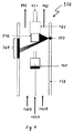
図1は、本発明を適用可能なHVPE装置の基本構成の一例を断面図で概略的に示す。本発明を適用可能な実施形態に係るHVPE装置20は、石英リアクタ21、それを取り囲む多分割炉(multi-zone furnace)22、矢印によって示されるガス供給源23及び23’、及び矢印によって示されるポンプ及び排気システム24を含む。基板ホルダ26上のテンプレート16は、フランジ25の装着や取出を通してリアクタ内に導入される。ポンプ及び排気システム24によって、リアクタは、その後、適切な1000mbar以下の範囲であって例えば約950mbarという所望のプロセス圧力に達する。多分割炉は、基板の表面上の成長温度を設定する第1の区域22Aと、Ga井戸28の領域の温度を設定する第2の区域22Bとを有する。キャリアガスとしてのH2及び/又はN2は、ガス供給源23及び23’を介してリアクタに供給される。塩化ガリウムをその場で生じさせるため、Ga井戸内に存在するGaは、多分割炉22の区域22B内の適切な温度を、例えば850℃に設定することによって気化され、適切なガス混合比及び適切な流量でH2/N2キャリアガスを使用してガス供給源23から流入したHClと反応する。その場で生じた塩化ガリウムは、リアクタ21内への流入チューブ23の端部にある開口部から流出する。そしてそこで、例えば約6〜7×103PaのNH3分圧を確立するのに適切なガス混合比及び適切な流量で、H2/N2キャリアガス混合物とともに流入チューブ23’から流入させたNH3と混合される。図1の下部の温度プロファイルから明らかなように、適切には約950〜1100℃、例えば約1050℃の基板温度を設定するため、多分割炉22の区域22A内では、区域22Bよりも高い温度が確立される。GaNは、基板ホルダ上に堆積される。仮に、例えば(Ga、Al、In)N層、(Ga、Al)N層、又は(Ga、In)N層がGaN層の代わりに堆積される場合、追加のAl井戸及び/又はIn井戸がHVPE装置20内に設けられる。したがって、例えばH2/N2の適切なキャリアガス中にHClを供給した結果として、図1のGa用の流入チューブ23を用いて説明したのと同様に、対応する塩化アルミニウム及び/又は塩化インジウムのリアクタ内への流入が生じる。
FIG. 1 schematically shows an example of a basic configuration of an HVPE apparatus to which the present invention is applicable in a cross-sectional view. An
HVPEによって堆積される層の成長は、動的成長測定及び成長制御によって、例えば50〜700μm/hの範囲内、好ましくは200〜500μm/hの範囲内の規定値に一定に維持された成長速度で、所望の層厚が実現されるまで継続される。動的成長測定及び制御のため、基板ホルダ26は、適切な測定デバイス27、例えば他の特定の実施形態においてさらに詳細にそれぞれ後述されるように、計量モジュール又は超音波エミッタ及び検出器ユニットを含む。ライン29を介して、このように測定精度内で判定される成長速度の値は、コンピュータユニット又はCPU(コントローラ)30に送られる。仮に、コンピュータユニット又はCPU30が、事前設定されたノミナルな成長速度と比べて、例えば2%の規定された許容できない閾値を超えるかもしれない検出可能な実測値の差異を検出した場合、コンピュータユニット又はCPU(コントローラ)30は、測定された実際の成長速度と事前設定されたノミナルな成長速度との間の差異が規定された許容できない閾値を下回るまで、成長速度のパラメータを制御する信号31を送る。信号31は、成長速度に影響する一又は複数の適切なプロセスパラメータを適切に制御し、最も有効には、フローパラメータ、特にHCl流量及び/又はHCl/NH3流量比を制御する。このようにして、例えば200μg以上の範囲、好ましくは300〜30.000μmの範囲の厚さを有する厚い層を、効率的にかつ優れた結晶均質性で得ることができる。
The growth of layers deposited by HVPE is maintained at a constant growth rate by dynamic growth measurement and growth control, for example, at a specified value in the range of 50 to 700 μm / h, preferably in the range of 200 to 500 μm / h. And so on until the desired layer thickness is achieved. For dynamic growth measurement and control, the substrate holder 26 includes a suitable measurement device 27, such as a metering module or ultrasonic emitter and detector unit, respectively as described in more detail below in other specific embodiments. . The value of the growth rate thus determined within the measurement accuracy is sent to the computer unit or CPU (controller) 30 via the
あるいは、成長速度の制御調整を、手動で、好ましくはHCl流量を調整することによって行うこともできる。 Alternatively, growth rate control adjustments can be made manually, preferably by adjusting the HCl flow rate.
図2〜4は、HVPE装置の変更された構成を概略的に示す断面図であり、特定の実施形態では、成長速度のその場での測定を異なる方法を使用することによって行うことができる。異なる測定方法は、図2では計量モジュール、図3では超音波エミッタ・検出器ユニット、図4では投影原理を用いて説明されている。 FIGS. 2-4 are cross-sectional views schematically illustrating a modified configuration of the HVPE apparatus, and in certain embodiments, in-situ measurement of growth rate can be performed by using different methods. The different measuring methods are explained using the weighing module in FIG. 2, the ultrasonic emitter / detector unit in FIG. 3, and the projection principle in FIG.
図2は、統合された計量モジュール110を有する垂直HVPEリアクタ100の概略的な構成を示す。ここで、計量モジュール110は、固定のサセプタホルダ121とサセプタ120の間に位置し、サセプタ120は、それに固定されかつその上にエピタキシャル層を成長させた基板150を有する。したがって、計量モジュール110は、サセプタ120と成長した基板150とを計量する。HVPEリアクタ100に関して、リアクタ壁130と、HCl及びキャリアガスのガス流入(下部中央の矢印140Aを参照)並びにNH3及びキャリアガスのガス流入(下部外側の2つの矢印140Bを参照)と、Ga源141と、排気ガスのためのガス流出口(上部外側の矢印142を参照)とがさらに示される。計量モジュールの使用は、基板を横にした水平リアクタについても同様に可能であり、その際、成長しているエピタキシャル層がその上にある基板を含むサセプタは、この場合もやはり計量される。図示される以下の実施形態では、図2のHVPEリアクタ100の要素と同一の、又はそれらに対応する要素は、同じ参照番号によって示され、したがってそれらの説明は省略する。
FIG. 2 shows a schematic configuration of a
図3は、統合された超音波エミッタ・検出器(ここでは共通の参照番号210によって示される)を含む、垂直HVPEリアクタ200の概略的な構成を示す。超音波エミッタ・検出器210は基板250の上方に位置する。層厚は、ここでは、基板250の成長表面250Aで反射されている超音波215の持続時間又は移動時間によって決定される。この検出された持続時間又は移動時間は、エピタキシャル成長の速度を表す。超音波測定の使用は、同様に、横になった基板を有する水平リアクタについても可能である。
FIG. 3 shows a schematic configuration of a
図4は、投影原理に基づいた統合された層厚測定を含む、垂直HVPEリアクタ300の概略的な構成を示す。ここで、III−N結晶310は、光源350、例えば、リアクタ壁130内に一体化することができる又はそれとは独立に設けられてもよい発光ダイオード若しくはレーザーダイオードで横方向に照明され、光は、CCDカメラなどの適切な検出器360によって反対側で局所的に検出される。なお、検出器360は、やはりリアクタ壁310内に一体化されてもよく、それとは独立に設けられてもよい。ここで、結晶の影は、増加する結晶長さに伴って検出器360全体にわたって移動する。影の移動速度は成長速度の検出値を示す。
FIG. 4 shows a schematic configuration of a
選択された方法によって決定された成長速度は、成長工程中に、成長速度を動的に制御するために使用される。このため、III族の原料ガスの制御に関与する電子マスフローコントローラ(MFC)に対するアクセスが行われる。GaNバルク結晶の結晶成長の場合、Ga源の上又は中を流れるHClガス流を制御するのはMFCである。さらに、N含有ガス(例えば、NH3)など他のガス流も、所望であればこのようにして調整することができる。例えば、V−III比をこのようにして一定に維持することができる。 The growth rate determined by the selected method is used to dynamically control the growth rate during the growth process. For this reason, access is made to an electronic mass flow controller (MFC) involved in the control of the group III source gas. In the case of GaN bulk crystal growth, it is the MFC that controls the HCl gas flow that flows over or in the Ga source. In addition, other gas flows such as N-containing gases (eg, NH 3 ) can be adjusted in this way if desired. For example, the V-III ratio can be kept constant in this way.
その後に、成長温度又は他の温度でアニーリング工程をさらに適用するとよい。 Thereafter, an annealing step may be further applied at the growth temperature or other temperature.
例えば円形研削、整列化などの一又は複数のプロセス工程の後、好ましくはワイヤ切断によって、成長したIII−Nバルク結晶を個別化することができる。個別化されたIII−N基板を、例えばラッピング、研磨、エッジ面取り、平坦部もしくは切欠きの研磨、アニーリング、及び/又は様々な仕上げ工程を含むさらなるプロセス工程後に得ることもできる。一般に、ラッピング及び研磨工程は多工程のプロセスである。 After one or more process steps, such as circular grinding, alignment, etc., the grown III-N bulk crystal can be individualized, preferably by wire cutting. Individualized III-N substrates can also be obtained after further process steps including, for example, lapping, polishing, edge chamfering, flat or notch polishing, annealing, and / or various finishing steps. In general, the lapping and polishing process is a multi-step process.
成長したIII−Nバルク結晶並びにその後のプロセス工程によって得られるIII−N基板は、記載したように成長速度をリアルタイムで測定し制御することによって、優れた結晶の質と、特に成長方向及びそれに垂直な平面内におけるその均等な配列を示す。 Grown III-N bulk crystals and III-N substrates obtained by subsequent process steps have excellent crystal quality, especially in the growth direction and perpendicular to it, by measuring and controlling the growth rate in real time as described. The equivalent arrangement in a flat plane is shown.
方法論的に、この結晶の質の特徴は、例えばX線回折によって、例えば特定の格子面における回折に相当する、X線回折曲線の絶対値及び/又は半値全幅の空間分布として決定され得る。成長面又は結晶表面における結晶の質の均質性は、例えば、成長面又は結晶表面に平行な面内で記録された、いわゆるX線ロッキング曲線マッピング(サンプルの異なる場所におけるω走査の記録)によって確認され得る。[0001]方向での成長の場合、例えば、[0002]格子面の反射をω走査に使用することができる。
成長方向における結晶の質の均質性は、対応するバルク結晶から得られた単体基板の[0002]走査における半値全幅の標準偏差によって判定されてもよい。
Methodologically, this crystal quality characteristic can be determined, for example, by X-ray diffraction, for example as a spatial distribution of the absolute value and / or full width at half maximum of the X-ray diffraction curve, corresponding to diffraction at a particular lattice plane. The homogeneity of the quality of the crystal at the growth surface or crystal surface is confirmed, for example, by so-called X-ray rocking curve mapping (recording of ω scans at different locations of the sample) recorded in a plane parallel to the growth surface or crystal surface Can be done. In the case of growth in the [0001] direction, for example, reflection of the [0002] lattice plane can be used for ω scanning.
Crystal quality homogeneity in the growth direction may be determined by the standard deviation of the full width at half maximum in a [0002] scan of a single substrate obtained from the corresponding bulk crystal.
あるいは、成長方向における結晶の質の均質性は、その表面が成長方向に向いている面内で記録されたロッキング曲線マッピングによって確認されてもよい。[0001]方向での成長の場合、例えば、m面(すなわち、{1100}又は{(1010)、(0110)、(1100)、(1010)、(0110)、(1100)}から選択された面)における反射が走査に使用されてもよく、そのマッピングは、対応するm面で、又は0〜10°のオフ角だけ対応するm面に向かって僅かに配向ずれしている面上で行われてもよい。 Alternatively, crystal quality homogeneity in the growth direction may be confirmed by rocking curve mapping recorded in a plane whose surface is oriented in the growth direction. In the case of growth in the [0001] direction, for example, selected from the m-plane (ie, {1100} or {(1010), (0110), (1100), (1010), (0110), (1100)}) Reflection on the surface) may be used for scanning, and the mapping is performed on the corresponding m-plane or on a surface that is slightly misoriented towards the corresponding m-plane by an off angle of 0-10 °. It may be broken.
結晶の質の均質性を決定するための第2の方法はマイクロラマンマッピングである。したがって、例えば、成長平面に平行な又は成長方向の走査におけるE2フォノンの周波数及び半値全幅の標準偏差は、それぞれ、成長平面に平行な又は成長方向内の結晶の質の均質性を表す。成長方向におけるバルク結晶の質の均質性は、同様に、好ましくは、対応するバルク結晶から得られた単一の基板のE2フォノンにおける半値全幅の平均値の標準偏差によって決定されてもよい。 A second method for determining crystal quality homogeneity is micro-Raman mapping. Thus, for example, the standard deviation of the frequency and full width at half maximum of the E 2 phonon in a scan parallel to the growth plane or in the growth direction represents the homogeneity of the crystal quality parallel to or in the growth direction, respectively. Homogeneity of the quality of the bulk crystal in the growth direction likewise preferably, may be determined by the standard deviation of the mean value of the full width at half maximum of E 2 phonon single substrate obtained from the corresponding bulk crystal.
[実施例]
直径が50〜60mmのGaN基板を、Aixtron LP−HVPEリアクタに装填する。基板ホルダ及びサセプタを含む結晶の重量を測定する計量モジュール又はロードセルによって、成長しているGaNバルク結晶の重量をリアルタイムで検出できるように、リアクタを変更する。ビーム偏向及び抵抗力フィードバックを備えたプラットフォーム計量モジュールの幾何学形状に基づくロードセルは、Hottinger Baldwin Meβtechnik GmbH(ドイツ、ダルムシュタット(Darmstadt))のタイプS2のロードセルである。出力信号は測定アンプによって処理する。厚さ数mmのバルクGaN結晶を基板上に成長させる。例えば、HVPEプロセスは、1040℃〜1075℃の温度及び900〜1000mbarの圧力、約50のV/III比、おおよそ水素50%と窒素50%のキャリアガス組成で行う。成長速度は220μm/hであり、リアルタイムで測定し、Ga源の中/上を通る塩化水素ガス流を調整することによってその場で制御する。
[Example]
A GaN substrate with a diameter of 50-60 mm is loaded into an Aixtron LP-HVPE reactor. The reactor is modified so that the weight of the growing GaN bulk crystal can be detected in real time by a weighing module or load cell that measures the weight of the crystal including the substrate holder and susceptor. The load cell based on the geometry of the platform weighing module with beam deflection and resistive feedback is a type S2 load cell from Hotterer Baldwin Meβtechnik GmbH (Darmstadt, Germany). The output signal is processed by the measuring amplifier. A bulk GaN crystal having a thickness of several mm is grown on the substrate. For example, the HVPE process is performed at a temperature of 1040 ° C. to 1075 ° C. and a pressure of 900 to 1000 mbar, a V / III ratio of about 50, and a carrier gas composition of approximately 50% hydrogen and 50% nitrogen. The growth rate is 220 μm / h, measured in real time and controlled in situ by adjusting the hydrogen chloride gas flow through / on the Ga source.
ロッキング曲線マッピングは、Cu Kα1ビームで動作し、内方コリメーティング光学系(inward collimating optic)を有する、高分解能の市販のX線回折計を用いて記録される。回折計は、装置によるロッキング曲線の広がりが50%未満であるように最適化する。ωの増分は、少なくとも20個の測定点が半値全幅内にあるように選択する。サンプル表面上の測定では、[0002]反射を使用し、x方向及びy方向の増分は約3mmである。表面上におけるX線ビームの焦点の横寸法は3mm以下である。ウェハ縁部から2mmの余白は測定から除外する。 Rocking curve mapping is recorded using a high resolution commercial X-ray diffractometer operating with Cu Kα 1 beam and having an inward collimating optic. The diffractometer is optimized so that the rocking curve spread by the instrument is less than 50%. The increment of ω is selected so that at least 20 measurement points are within the full width at half maximum. For measurements on the sample surface, [0002] reflection is used and the increments in the x and y directions are about 3 mm. The lateral dimension of the focal point of the X-ray beam on the surface is 3 mm or less. A margin of 2 mm from the wafer edge is excluded from the measurement.
マイクロラマン測定は、532nmのレーザー励起波長(周波数二倍器Nd:YAGレーザー)、3mWの励起電力で、並びにJobin YvonのLlabram800HR分光計を用いて実施し、その際、レーザーは、顕微鏡光学系によって約1μmのビーム直径までサンプル上に集束される。分光計は、Neプラズマ線によってさらに校正する。測定は、裏面走査配置で実施し、その際、偏光子設定は、E2フォノンを検出できるように選択する(表面上の走査はz(y x/y)−z、スリット面上の走査はy(x x)−y)。表面上を走査するとき、x方向及びy方向の増分は約2.5mmである。ウェハ縁部から2mmの余白は測定から除外する。表面に垂直なウェハスリット面上を走査するとき、z方向の増分は約10μmである。E2フォノンの周波数及び半値全幅は、ローレンツ線形状分析によって検出する。 Micro-Raman measurements were performed at a laser excitation wavelength of 532 nm (frequency doubler Nd: YAG laser), with an excitation power of 3 mW, as well as with a Jobin Ylab Llabram 800HR spectrometer, with the laser being controlled by the microscope optics. Focused on the sample to a beam diameter of about 1 μm. The spectrometer is further calibrated with Ne plasma lines. Measurement was carried out at the back side scanning arrangement, in which, polarizer settings, E 2 phonon selected to so as to detect the (scanning on the surface z (y x / y) -z , the scanning on slit plane y (xx) -y). When scanning over the surface, the increment in the x and y directions is about 2.5 mm. A margin of 2 mm from the wafer edge is excluded from the measurement. When scanning over the wafer slit plane perpendicular to the surface, the z-direction increment is about 10 μm. The frequency and full width at half maximum of E 2 phonon are detected by Lorentz line shape analysis.
上述の様々な態様、利点、実施形態、及び実施例の特徴を、所望の組み合わせで実施することができる。 The various aspects, advantages, embodiments, and example features described above can be implemented in any desired combination.
Claims (6)
IIIは、周期表のIII族のうちAl、Ga及びInから選択された少なくとも1つの元素を指し、
前記III−Nバルク結晶を、ハイドライド気相成長法によって基板又はテンプレート上に成長させ、
前記III−Nバルク結晶の成長速度がリアルタイムで測定され、前記III−Nバルク結晶の成長最前面の位置がリアルタイム制御によって一定に維持され、
実際の成長速度を、エピタキシャル成長の間少なくとも一の値で本質的に一定に維持するように、成長速度をリアルタイムで測定して動的に制御して、
前記結晶の重量、又は前記結晶にサセプタを含む結晶ホルダを加えたものの重量を計る方法によって、成長速度が測定又は決定される
ことを特徴とするIII−Nバルク結晶の製造方法。 A method for producing a III-N bulk crystal comprising:
III refers to at least one element selected from Al, Ga and In among group III of the periodic table;
The III-N bulk crystal is grown on a substrate or template by a hydride vapor phase growth method,
The growth rate of the III-N bulk crystal is measured in real time, and the position of the forefront growth of the III-N bulk crystal is kept constant by real time control,
In order to keep the actual growth rate essentially constant at at least one value during epitaxial growth, the growth rate is measured in real time and dynamically controlled,
A method for producing a III-N bulk crystal, wherein a growth rate is measured or determined by a method of measuring a weight of the crystal or a crystal holder including a susceptor added to the crystal.
c面、a面、m面、又はr面に対して0.1〜30°のオフ角(ミスカット)を有する成長面又は成長表面を有するIII−N基板が前記III−Nバルク結晶を成長させる基板として使用され、前記III−Nバルク結晶がその上に堆積される
ことを特徴とするIII−Nバルク結晶の製造方法。 In the manufacturing method of the III-N bulk crystal of Claim 1,
A III-N substrate having a growth surface or growth surface having an off angle (miscut) of 0.1 to 30 ° with respect to the c-plane, a-plane, m-plane, or r-plane grows the III-N bulk crystal. A method for producing a III-N bulk crystal, wherein the III-N bulk crystal is used as a substrate to be deposited, and the III-N bulk crystal is deposited thereon.
実際の成長速度と所望の成長速度とを比べたときに最大で10%の差を検出したとき、実際に一定した成長速度への修正又は調整が行われる
ことを特徴とするIII−Nバルク結晶の製造方法。 In the manufacturing method of the III-N bulk crystal of Claim 1,
A III-N bulk crystal characterized in that a correction or adjustment to an actually constant growth rate is performed when a maximum difference of 10% is detected when comparing an actual growth rate with a desired growth rate. Manufacturing method.
前記成長させたIII−Nバルク結晶は、円形又は略円形の断面を有し、
前記円形の断面は、5cm以上の直径を有する
ことを特徴とするIII−Nバルク結晶の製造方法。 In the manufacturing method of the III-N bulk crystal as described in any one of Claims 1-3,
The grown III-N bulk crystal has a circular or substantially circular cross section;
The method for producing a III-N bulk crystal, wherein the circular cross section has a diameter of 5 cm or more.
前記成長させたIII−Nバルク結晶の長さは、1mm以上である
ことを特徴とするIII−Nバルク結晶の製造方法。 In the manufacturing method of the III-N bulk crystal as described in any one of Claims 1-4,
The length of said grown III-N bulk crystal is 1 mm or more, The manufacturing method of the III-N bulk crystal characterized by the above-mentioned.
サファイア、炭化シリコン、砒化ガリウム、アルミン酸リチウム又はシリコンの単結晶形がそれぞれ前記III−Nバルク結晶を成長させる基板として使用され、
前記III−Nバルク結晶を、その基板上に又はその基板を含むテンプレート上に成長させる
ことを特徴とするIII−Nバルク結晶の製造方法。 In the manufacturing method of the III-N bulk crystal as described in any one of Claims 1-5,
Single crystal forms of sapphire, silicon carbide, gallium arsenide, lithium aluminate or silicon are each used as a substrate for growing the III-N bulk crystal,
A method for producing a III-N bulk crystal, comprising growing the III-N bulk crystal on a substrate or a template including the substrate.
Applications Claiming Priority (3)
| Application Number | Priority Date | Filing Date | Title |
|---|---|---|---|
| US79831406P | 2006-05-08 | 2006-05-08 | |
| US60/798,314 | 2006-05-08 | ||
| PCT/EP2007/003961 WO2007128522A2 (en) | 2006-05-08 | 2007-05-04 | Process for producing a iii-n bulk crystal and a free-standing iii -n substrate, and iii -n bulk crystal and free-standing ih-n substrate |
Publications (2)
| Publication Number | Publication Date |
|---|---|
| JP2009536139A JP2009536139A (en) | 2009-10-08 |
| JP5656401B2 true JP5656401B2 (en) | 2015-01-21 |
Family
ID=38198100
Family Applications (1)
| Application Number | Title | Priority Date | Filing Date |
|---|---|---|---|
| JP2009508221A Active JP5656401B2 (en) | 2006-05-08 | 2007-05-04 | III-N Bulk Crystal and Freestanding III-N Substrate Manufacturing Method, and III-N Bulk Crystal and Freestanding III-N Substrate |
Country Status (7)
| Country | Link |
|---|---|
| US (1) | US8048224B2 (en) |
| EP (1) | EP2016209B1 (en) |
| JP (1) | JP5656401B2 (en) |
| CN (2) | CN101443488B (en) |
| DE (1) | DE602007011917D1 (en) |
| PL (1) | PL2016209T3 (en) |
| WO (1) | WO2007128522A2 (en) |
Families Citing this family (24)
| Publication number | Priority date | Publication date | Assignee | Title |
|---|---|---|---|---|
| US9909230B2 (en) * | 2006-04-07 | 2018-03-06 | Sixpoint Materials, Inc. | Seed selection and growth methods for reduced-crack group III nitride bulk crystals |
| SG174771A1 (en) * | 2006-06-09 | 2011-10-28 | Soitec Silicon On Insulator | High volume delivery system for gallium trichloride |
| US8778078B2 (en) * | 2006-08-09 | 2014-07-15 | Freiberger Compound Materials Gmbh | Process for the manufacture of a doped III-N bulk crystal and a free-standing III-N substrate, and doped III-N bulk crystal and free-standing III-N substrate as such |
| US9481944B2 (en) | 2006-11-22 | 2016-11-01 | Soitec | Gas injectors including a funnel- or wedge-shaped channel for chemical vapor deposition (CVD) systems and CVD systems with the same |
| WO2008064077A2 (en) | 2006-11-22 | 2008-05-29 | S.O.I.Tec Silicon On Insulator Technologies | Methods for high volume manufacture of group iii-v semiconductor materials |
| US9580836B2 (en) | 2006-11-22 | 2017-02-28 | Soitec | Equipment for high volume manufacture of group III-V semiconductor materials |
| US9481943B2 (en) | 2006-11-22 | 2016-11-01 | Soitec | Gallium trichloride injection scheme |
| EP2084304B1 (en) | 2006-11-22 | 2013-06-26 | Soitec | Method and apparatus for the epitaxial deposition of monocrystalline group iii-v semiconductor material using gallium trichloride |
| WO2008064080A1 (en) * | 2006-11-22 | 2008-05-29 | S.O.I.Tec Silicon On Insulator Technologies | High volume delivery system for gallium trichloride |
| KR101390425B1 (en) | 2006-11-22 | 2014-05-19 | 소이텍 | Temperature-controlled Purge gate valve for Chemical Vapor Deposition Chamber |
| WO2008101625A1 (en) * | 2007-02-23 | 2008-08-28 | Freiberger Compounds Materials Gmbh | Method for producing (al,ga)n crystals |
| JP5045388B2 (en) * | 2007-11-20 | 2012-10-10 | 住友電気工業株式会社 | Group III nitride semiconductor crystal growth method and group III nitride semiconductor crystal substrate manufacturing method |
| JP2009126723A (en) * | 2007-11-20 | 2009-06-11 | Sumitomo Electric Ind Ltd | Growing method of group iii nitride semiconductor crystal, fabrication method of group iii nitride semiconductor crystal substrate, and group iii nitride semiconductor crystal substrate |
| JP5018423B2 (en) * | 2007-11-20 | 2012-09-05 | 住友電気工業株式会社 | Group III nitride semiconductor crystal substrate and semiconductor device |
| JP5251893B2 (en) * | 2010-01-21 | 2013-07-31 | 日立電線株式会社 | Method for producing conductive group III nitride crystal and method for producing conductive group III nitride substrate |
| JP2011213557A (en) * | 2010-04-01 | 2011-10-27 | Hitachi Cable Ltd | Method for producing conductive group iii nitride single crystal substrate |
| US20130000545A1 (en) * | 2011-06-28 | 2013-01-03 | Nitride Solutions Inc. | Device and method for producing bulk single crystals |
| TWI684680B (en) | 2013-09-04 | 2020-02-11 | 奈瑞德解決方案公司 | Bulk diffusion crystal growth process |
| EP3247824A1 (en) * | 2015-01-22 | 2017-11-29 | SixPoint Materials, Inc. | Seed selection and growth methods for reduced-crack group iii nitride bulk crystals |
| CN107740183A (en) * | 2017-10-12 | 2018-02-27 | 北京大学 | A kind of high temperature clean chamber system and method suitable for AlN crystal growths |
| WO2019167337A1 (en) * | 2018-03-01 | 2019-09-06 | 住友電気工業株式会社 | Silicon carbide substrate |
| US12046471B1 (en) * | 2018-06-06 | 2024-07-23 | United States Of America As Represented By The Secretary Of The Air Force | Optimized thick heteroepitaxial growth of semiconductors with in-situ substrate pretreatment |
| WO2023214590A1 (en) * | 2022-05-06 | 2023-11-09 | 株式会社福田結晶技術研究所 | Method for manufacturing high-quality, low-cost, free-standing gan substrate |
| WO2024075328A1 (en) * | 2022-10-06 | 2024-04-11 | 日本碍子株式会社 | Group iii element nitride semiconductor substrate |
Family Cites Families (13)
| Publication number | Priority date | Publication date | Assignee | Title |
|---|---|---|---|---|
| JPS643503A (en) * | 1987-06-25 | 1989-01-09 | Fujitsu Ltd | Method for measuring thickness of crystal layer |
| JPH04154699A (en) * | 1990-10-17 | 1992-05-27 | Asahi Chem Ind Co Ltd | Synthesis of iii-v group element compound single crystal thin film |
| JPH08148438A (en) * | 1994-11-24 | 1996-06-07 | Hitachi Cable Ltd | Method and device for vapor growth of compound semiconductor thin film crystal |
| FR2769924B1 (en) * | 1997-10-20 | 2000-03-10 | Centre Nat Rech Scient | PROCESS FOR MAKING AN EPITAXIAL LAYER OF GALLIUM NITRIDE, EPITAXIAL LAYER OF GALLIUM NITRIDE AND OPTOELECTRONIC COMPONENT PROVIDED WITH SUCH A LAYER |
| WO2001065592A2 (en) * | 2000-03-02 | 2001-09-07 | Aixtron Ag | Method and device for producing group iii-n, group iii-v-n and metal-nitrogen component structures on si substrates |
| US6596079B1 (en) | 2000-03-13 | 2003-07-22 | Advanced Technology Materials, Inc. | III-V nitride substrate boule and method of making and using the same |
| TW546850B (en) * | 2000-08-18 | 2003-08-11 | Showa Denko Kk | Manufacturing method for crystallization of group III nitride semiconductor, manufacturing method for gallium nitride compound semiconductor, gallium nitride compound semiconductor, gallium nitride compound semiconductor light emitting elements and light |
| US20030205193A1 (en) * | 2001-07-06 | 2003-11-06 | Melnik Yuri V. | Method for achieving low defect density aigan single crystal boules |
| US6616757B1 (en) * | 2001-07-06 | 2003-09-09 | Technologies And Devices International, Inc. | Method for achieving low defect density GaN single crystal boules |
| US6936357B2 (en) * | 2001-07-06 | 2005-08-30 | Technologies And Devices International, Inc. | Bulk GaN and ALGaN single crystals |
| ATE335872T1 (en) * | 2003-04-24 | 2006-09-15 | Norstel Ab | DEVICE AND METHOD FOR PRODUCING SINGLE CRYSTALS BY VAPOR PHASE DEPOSITION |
| JP4513326B2 (en) * | 2004-01-14 | 2010-07-28 | 日立電線株式会社 | Nitride semiconductor crystal manufacturing method and nitride semiconductor substrate manufacturing method |
| JP3888374B2 (en) * | 2004-03-17 | 2007-02-28 | 住友電気工業株式会社 | Manufacturing method of GaN single crystal substrate |
-
2007
- 2007-05-04 JP JP2009508221A patent/JP5656401B2/en active Active
- 2007-05-04 EP EP07724886A patent/EP2016209B1/en active Active
- 2007-05-04 CN CN2007800168710A patent/CN101443488B/en not_active Expired - Fee Related
- 2007-05-04 CN CN201110332897.4A patent/CN102358955B/en active Active
- 2007-05-04 DE DE602007011917T patent/DE602007011917D1/en active Active
- 2007-05-04 WO PCT/EP2007/003961 patent/WO2007128522A2/en active Application Filing
- 2007-05-04 PL PL07724886T patent/PL2016209T3/en unknown
- 2007-05-07 US US11/745,239 patent/US8048224B2/en active Active
Also Published As
| Publication number | Publication date |
|---|---|
| EP2016209B1 (en) | 2011-01-12 |
| CN101443488B (en) | 2013-03-27 |
| US8048224B2 (en) | 2011-11-01 |
| CN102358955B (en) | 2014-06-25 |
| WO2007128522A2 (en) | 2007-11-15 |
| DE602007011917D1 (en) | 2011-02-24 |
| CN102358955A (en) | 2012-02-22 |
| WO2007128522A3 (en) | 2008-01-10 |
| CN101443488A (en) | 2009-05-27 |
| US20070257334A1 (en) | 2007-11-08 |
| JP2009536139A (en) | 2009-10-08 |
| EP2016209A2 (en) | 2009-01-21 |
| PL2016209T3 (en) | 2011-06-30 |
Similar Documents
| Publication | Publication Date | Title |
|---|---|---|
| JP5656401B2 (en) | III-N Bulk Crystal and Freestanding III-N Substrate Manufacturing Method, and III-N Bulk Crystal and Freestanding III-N Substrate | |
| JP5544172B2 (en) | Manufacturing method of semiconductor composite material using vapor phase epitaxy | |
| JP5725086B2 (en) | Group III nitride semiconductor crystal manufacturing method, group III nitride semiconductor substrate, and semiconductor light emitting device | |
| US7847313B2 (en) | Group III-V nitride-based semiconductor substrate and group III-V nitride-based light emitting device | |
| US8137825B2 (en) | Aluminum nitride single crystal film, aluminum nitride single crystal multi-layer substrate and manufacturing processes thereof | |
| US20110018104A1 (en) | METHOD FOR PRODUCING A LAMINATED BODY HAVING Al-BASED GROUP-III NITRIDE SINGLE CRYSTAL LAYER, LAMINATED BODY PRODUCED BY THE METHOD, METHOD FOR PRODUCING Al-BASED GROUP-III NITRIDE SINGLE CRYSTAL SUBSTRATE EMPLOYING THE LAMINATED BODY, AND ALUMINUM NITRIDE SINGLE CRYSTAL SUBSTRATE | |
| US9461121B2 (en) | Process for the manufacture of a doped III-N bulk crystal and a free-standing III-N substrate, and doped III-N bulk crystal and free-standing III-N substrate as such | |
| US20190287799A1 (en) | Apparatus for manufacturing group iii nitride single crystal, method for manufacturing group iii nitride single crystal using the apparatus, and aluminum nitride single crystal | |
| WO2006013957A1 (en) | NITRIDE SEMICONDUCTOR SINGLE CRYSTAL INCLUDING Ga, METHOD FOR MANUFACTURING THE SAME, AND SUBSTRATE AND DEVICE USING THE CRYSTAL | |
| JP5298015B2 (en) | Method for producing doped III-N bulk crystal and free-standing doped III-N substrate | |
| US7348278B2 (en) | Method of making nitride-based compound semiconductor crystal and substrate | |
| JP2019218263A (en) | METHOD FOR MANUFACTURING GaN CRYSTAL | |
| JP2005145754A (en) | Nitride semiconductor substrate and its manufacturing method | |
| US20100307405A1 (en) | Method for Growing AlxGa1-xN Single Crystal | |
| JP2013049621A (en) | Nitride semiconductor crystal, growing method thereof, material, and gallium nitride single crystal substrate | |
| JP5629340B2 (en) | Doped III-N bulk crystal and free-standing doped III-N substrate | |
| JP6916719B2 (en) | Method for producing Group III nitride single crystal laminate and Group III nitride single crystal laminate | |
| WO2016194931A1 (en) | In-situ observation device of substrate warpage and crystal growth apparatus |
Legal Events
| Date | Code | Title | Description |
|---|---|---|---|
| A621 | Written request for application examination |
Free format text: JAPANESE INTERMEDIATE CODE: A621 Effective date: 20100223 |
|
| A977 | Report on retrieval |
Free format text: JAPANESE INTERMEDIATE CODE: A971007 Effective date: 20120618 |
|
| A131 | Notification of reasons for refusal |
Free format text: JAPANESE INTERMEDIATE CODE: A131 Effective date: 20120703 |
|
| A521 | Request for written amendment filed |
Free format text: JAPANESE INTERMEDIATE CODE: A523 Effective date: 20121003 |
|
| A131 | Notification of reasons for refusal |
Free format text: JAPANESE INTERMEDIATE CODE: A131 Effective date: 20130709 |
|
| A601 | Written request for extension of time |
Free format text: JAPANESE INTERMEDIATE CODE: A601 Effective date: 20131008 |
|
| A602 | Written permission of extension of time |
Free format text: JAPANESE INTERMEDIATE CODE: A602 Effective date: 20131016 |
|
| A521 | Request for written amendment filed |
Free format text: JAPANESE INTERMEDIATE CODE: A523 Effective date: 20131021 |
|
| A131 | Notification of reasons for refusal |
Free format text: JAPANESE INTERMEDIATE CODE: A131 Effective date: 20140107 |
|
| A521 | Request for written amendment filed |
Free format text: JAPANESE INTERMEDIATE CODE: A523 Effective date: 20140404 |
|
| A02 | Decision of refusal |
Free format text: JAPANESE INTERMEDIATE CODE: A02 Effective date: 20140520 |
|
| A521 | Request for written amendment filed |
Free format text: JAPANESE INTERMEDIATE CODE: A523 Effective date: 20140908 |
|
| A521 | Request for written amendment filed |
Free format text: JAPANESE INTERMEDIATE CODE: A821 Effective date: 20140909 |
|
| A911 | Transfer to examiner for re-examination before appeal (zenchi) |
Free format text: JAPANESE INTERMEDIATE CODE: A911 Effective date: 20141001 |
|
| TRDD | Decision of grant or rejection written | ||
| A01 | Written decision to grant a patent or to grant a registration (utility model) |
Free format text: JAPANESE INTERMEDIATE CODE: A01 Effective date: 20141028 |
|
| A61 | First payment of annual fees (during grant procedure) |
Free format text: JAPANESE INTERMEDIATE CODE: A61 Effective date: 20141125 |
|
| R150 | Certificate of patent or registration of utility model |
Ref document number: 5656401 Country of ref document: JP Free format text: JAPANESE INTERMEDIATE CODE: R150 |
|
| R250 | Receipt of annual fees |
Free format text: JAPANESE INTERMEDIATE CODE: R250 |
|
| R250 | Receipt of annual fees |
Free format text: JAPANESE INTERMEDIATE CODE: R250 |
|
| R250 | Receipt of annual fees |
Free format text: JAPANESE INTERMEDIATE CODE: R250 |
|
| R250 | Receipt of annual fees |
Free format text: JAPANESE INTERMEDIATE CODE: R250 |
|
| R250 | Receipt of annual fees |
Free format text: JAPANESE INTERMEDIATE CODE: R250 |
|
| R250 | Receipt of annual fees |
Free format text: JAPANESE INTERMEDIATE CODE: R250 |
|
| R250 | Receipt of annual fees |
Free format text: JAPANESE INTERMEDIATE CODE: R250 |