JP5654760B2 - Optical element - Google Patents
Optical element Download PDFInfo
- Publication number
- JP5654760B2 JP5654760B2 JP2010044838A JP2010044838A JP5654760B2 JP 5654760 B2 JP5654760 B2 JP 5654760B2 JP 2010044838 A JP2010044838 A JP 2010044838A JP 2010044838 A JP2010044838 A JP 2010044838A JP 5654760 B2 JP5654760 B2 JP 5654760B2
- Authority
- JP
- Japan
- Prior art keywords
- semiconductor layer
- light
- optical element
- optical
- electrode
- Prior art date
- Legal status (The legal status is an assumption and is not a legal conclusion. Google has not performed a legal analysis and makes no representation as to the accuracy of the status listed.)
- Expired - Fee Related
Links
- 230000003287 optical effect Effects 0.000 title claims description 59
- 239000004065 semiconductor Substances 0.000 claims description 94
- 239000000758 substrate Substances 0.000 claims description 41
- 230000004888 barrier function Effects 0.000 claims description 17
- 238000001514 detection method Methods 0.000 claims description 17
- 230000008878 coupling Effects 0.000 claims description 10
- 238000010168 coupling process Methods 0.000 claims description 10
- 238000005859 coupling reaction Methods 0.000 claims description 10
- 239000006185 dispersion Substances 0.000 claims description 8
- 230000005540 biological transmission Effects 0.000 claims description 6
- 230000001678 irradiating effect Effects 0.000 claims description 4
- 239000000470 constituent Substances 0.000 claims description 3
- 230000005284 excitation Effects 0.000 description 32
- 239000000463 material Substances 0.000 description 9
- 238000000034 method Methods 0.000 description 9
- 230000005684 electric field Effects 0.000 description 8
- 229910000530 Gallium indium arsenide Inorganic materials 0.000 description 6
- 238000010586 diagram Methods 0.000 description 6
- 239000002184 metal Substances 0.000 description 6
- 229910052751 metal Inorganic materials 0.000 description 6
- 239000000523 sample Substances 0.000 description 6
- 239000010936 titanium Substances 0.000 description 6
- 229910001218 Gallium arsenide Inorganic materials 0.000 description 5
- 239000000835 fiber Substances 0.000 description 5
- 239000011347 resin Substances 0.000 description 5
- 229920005989 resin Polymers 0.000 description 5
- 239000000969 carrier Substances 0.000 description 4
- 238000004891 communication Methods 0.000 description 4
- 239000010453 quartz Substances 0.000 description 4
- VYPSYNLAJGMNEJ-UHFFFAOYSA-N silicon dioxide Inorganic materials O=[Si]=O VYPSYNLAJGMNEJ-UHFFFAOYSA-N 0.000 description 4
- XUIMIQQOPSSXEZ-UHFFFAOYSA-N Silicon Chemical compound [Si] XUIMIQQOPSSXEZ-UHFFFAOYSA-N 0.000 description 3
- 238000003384 imaging method Methods 0.000 description 3
- 238000005259 measurement Methods 0.000 description 3
- 229910052710 silicon Inorganic materials 0.000 description 3
- 239000010703 silicon Substances 0.000 description 3
- 238000000862 absorption spectrum Methods 0.000 description 2
- 150000001336 alkenes Chemical class 0.000 description 2
- 238000004458 analytical method Methods 0.000 description 2
- 230000015556 catabolic process Effects 0.000 description 2
- 239000013078 crystal Substances 0.000 description 2
- 238000005530 etching Methods 0.000 description 2
- 239000012535 impurity Substances 0.000 description 2
- 238000000691 measurement method Methods 0.000 description 2
- JRZJOMJEPLMPRA-UHFFFAOYSA-N olefin Natural products CCCCCCCC=C JRZJOMJEPLMPRA-UHFFFAOYSA-N 0.000 description 2
- 230000000704 physical effect Effects 0.000 description 2
- 230000005855 radiation Effects 0.000 description 2
- 239000000126 substance Substances 0.000 description 2
- 0 *C(C1)*1(CC1)CCC1=* Chemical compound *C(C1)*1(CC1)CCC1=* 0.000 description 1
- 239000004698 Polyethylene Substances 0.000 description 1
- 239000004809 Teflon Substances 0.000 description 1
- 229920006362 Teflon® Polymers 0.000 description 1
- RTAQQCXQSZGOHL-UHFFFAOYSA-N Titanium Chemical compound [Ti] RTAQQCXQSZGOHL-UHFFFAOYSA-N 0.000 description 1
- 239000000853 adhesive Substances 0.000 description 1
- 230000001070 adhesive effect Effects 0.000 description 1
- 230000003321 amplification Effects 0.000 description 1
- 238000011088 calibration curve Methods 0.000 description 1
- 230000008859 change Effects 0.000 description 1
- 239000011248 coating agent Substances 0.000 description 1
- 238000000576 coating method Methods 0.000 description 1
- 239000002772 conduction electron Substances 0.000 description 1
- 238000012937 correction Methods 0.000 description 1
- 230000007547 defect Effects 0.000 description 1
- 238000013461 design Methods 0.000 description 1
- 238000011161 development Methods 0.000 description 1
- 238000005553 drilling Methods 0.000 description 1
- 238000002296 dynamic light scattering Methods 0.000 description 1
- 238000005516 engineering process Methods 0.000 description 1
- 238000007689 inspection Methods 0.000 description 1
- 230000004048 modification Effects 0.000 description 1
- 238000012986 modification Methods 0.000 description 1
- 238000003199 nucleic acid amplification method Methods 0.000 description 1
- 230000035699 permeability Effects 0.000 description 1
- 238000005498 polishing Methods 0.000 description 1
- -1 polyethylene Polymers 0.000 description 1
- 229920000573 polyethylene Polymers 0.000 description 1
- 230000001902 propagating effect Effects 0.000 description 1
- 230000006798 recombination Effects 0.000 description 1
- 238000005215 recombination Methods 0.000 description 1
- 230000009467 reduction Effects 0.000 description 1
- 238000005070 sampling Methods 0.000 description 1
- 229910052594 sapphire Inorganic materials 0.000 description 1
- 239000010980 sapphire Substances 0.000 description 1
- 238000005549 size reduction Methods 0.000 description 1
- 238000012306 spectroscopic technique Methods 0.000 description 1
- 238000004611 spectroscopical analysis Methods 0.000 description 1
- 238000001228 spectrum Methods 0.000 description 1
- 238000001328 terahertz time-domain spectroscopy Methods 0.000 description 1
- 229910052719 titanium Inorganic materials 0.000 description 1
- 238000012546 transfer Methods 0.000 description 1
- 230000001131 transforming effect Effects 0.000 description 1
- 230000007704 transition Effects 0.000 description 1
- 238000002834 transmittance Methods 0.000 description 1
- 238000007740 vapor deposition Methods 0.000 description 1
Images


Classifications
-
- H—ELECTRICITY
- H01—ELECTRIC ELEMENTS
- H01L—SEMICONDUCTOR DEVICES NOT COVERED BY CLASS H10
- H01L27/00—Devices consisting of a plurality of semiconductor or other solid-state components formed in or on a common substrate
- H01L27/14—Devices consisting of a plurality of semiconductor or other solid-state components formed in or on a common substrate including semiconductor components sensitive to infrared radiation, light, electromagnetic radiation of shorter wavelength or corpuscular radiation and specially adapted either for the conversion of the energy of such radiation into electrical energy or for the control of electrical energy by such radiation
- H01L27/144—Devices controlled by radiation
- H01L27/1443—Devices controlled by radiation with at least one potential jump or surface barrier
-
- G—PHYSICS
- G01—MEASURING; TESTING
- G01J—MEASUREMENT OF INTENSITY, VELOCITY, SPECTRAL CONTENT, POLARISATION, PHASE OR PULSE CHARACTERISTICS OF INFRARED, VISIBLE OR ULTRAVIOLET LIGHT; COLORIMETRY; RADIATION PYROMETRY
- G01J3/00—Spectrometry; Spectrophotometry; Monochromators; Measuring colours
- G01J3/28—Investigating the spectrum
- G01J3/42—Absorption spectrometry; Double beam spectrometry; Flicker spectrometry; Reflection spectrometry
-
- H—ELECTRICITY
- H01—ELECTRIC ELEMENTS
- H01S—DEVICES USING THE PROCESS OF LIGHT AMPLIFICATION BY STIMULATED EMISSION OF RADIATION [LASER] TO AMPLIFY OR GENERATE LIGHT; DEVICES USING STIMULATED EMISSION OF ELECTROMAGNETIC RADIATION IN WAVE RANGES OTHER THAN OPTICAL
- H01S1/00—Masers, i.e. devices using stimulated emission of electromagnetic radiation in the microwave range
-
- H—ELECTRICITY
- H01—ELECTRIC ELEMENTS
- H01L—SEMICONDUCTOR DEVICES NOT COVERED BY CLASS H10
- H01L31/00—Semiconductor devices sensitive to infrared radiation, light, electromagnetic radiation of shorter wavelength or corpuscular radiation and specially adapted either for the conversion of the energy of such radiation into electrical energy or for the control of electrical energy by such radiation; Processes or apparatus specially adapted for the manufacture or treatment thereof or of parts thereof; Details thereof
- H01L31/08—Semiconductor devices sensitive to infrared radiation, light, electromagnetic radiation of shorter wavelength or corpuscular radiation and specially adapted either for the conversion of the energy of such radiation into electrical energy or for the control of electrical energy by such radiation; Processes or apparatus specially adapted for the manufacture or treatment thereof or of parts thereof; Details thereof in which radiation controls flow of current through the device, e.g. photoresistors
- H01L31/10—Semiconductor devices sensitive to infrared radiation, light, electromagnetic radiation of shorter wavelength or corpuscular radiation and specially adapted either for the conversion of the energy of such radiation into electrical energy or for the control of electrical energy by such radiation; Processes or apparatus specially adapted for the manufacture or treatment thereof or of parts thereof; Details thereof in which radiation controls flow of current through the device, e.g. photoresistors characterised by at least one potential-jump barrier or surface barrier, e.g. phototransistors
- H01L31/101—Devices sensitive to infrared, visible or ultraviolet radiation
- H01L31/102—Devices sensitive to infrared, visible or ultraviolet radiation characterised by only one potential barrier or surface barrier
- H01L31/108—Devices sensitive to infrared, visible or ultraviolet radiation characterised by only one potential barrier or surface barrier the potential barrier being of the Schottky type
Landscapes
- Physics & Mathematics (AREA)
- Spectroscopy & Molecular Physics (AREA)
- Electromagnetism (AREA)
- General Physics & Mathematics (AREA)
- Power Engineering (AREA)
- Engineering & Computer Science (AREA)
- Condensed Matter Physics & Semiconductors (AREA)
- Computer Hardware Design (AREA)
- Microelectronics & Electronic Packaging (AREA)
- Optics & Photonics (AREA)
- Investigating Or Analysing Materials By Optical Means (AREA)
- Light Receiving Elements (AREA)
- Optical Modulation, Optical Deflection, Nonlinear Optics, Optical Demodulation, Optical Logic Elements (AREA)
Description
本発明は、ミリ波帯からテラヘルツ波帯(30GHz〜30THz)までの周波数領域の成分を含むテラヘルツ波を発生または検出する光素子、及びそれを用いる装置に関する。特に、光パルス照射により前記周波数帯のフーリエ成分を含む電磁波パルスの発生または検出を行う光素子、それを用いたテラヘルツ時間領域分光装置(THz-TDS)等に関する。 The present invention relates to an optical element that generates or detects a terahertz wave including a component in a frequency region from a millimeter wave band to a terahertz wave band (30 GHz to 30 THz), and an apparatus using the same. In particular, the present invention relates to an optical element that generates or detects an electromagnetic wave pulse including a Fourier component in the frequency band by light pulse irradiation, a terahertz time domain spectroscopic device (THz-TDS) using the optical element, and the like.
近年、テラヘルツ波を用いた非破壊なセンシング技術が開発されている。この周波数帯の電磁波の応用分野として、X線装置に代わる安全な透視検査装置を構成してイメージングを行う技術がある。また、物質内部の吸収スペクトルや複素誘電率を求めて分子の結合状態などの物性を調べる分光技術、キャリア濃度や移動度、導電率などの物性を調べる計測技術、生体分子の解析技術などが開発されている。テラヘルツ波の発生方法としては、光伝導素子を用いる方法が広く用いられている。この光伝導素子は、典型的には、移動度が比較的大きくキャリア寿命がピコ秒以下という特殊な半導体と、その上の2つの電極とで構成される。電極間に電圧を印加した状態で電極間のギャップに超短パルス光を照射すると、励起された光キャリアにより電流が瞬間的に電極間を流れ、テラヘルツ波が放射される。この様な光伝導素子をテラヘルツ波の検出器としても用いてTHz- TDSを構成することで、上記の様な計測、イメージング技術が研究されている。こうした技術状況において、励起用の超短パルスレーザとして一般にチタンサファイアレーザが用いられるが、小型化、低コスト化のために、通信波長帯のファイバーレーザの利用が望まれている。この場合、励起光波長が1μm以上となり、これまで光伝導素子で用いていた低温成長(LT-)GaAsは、この波長に対して透明体となるために使用できない。そこで、LT-InGaAsがその代わりの光伝導材料として研究されている(特許文献1参照)。 In recent years, nondestructive sensing technology using terahertz waves has been developed. As an application field of electromagnetic waves in this frequency band, there is a technique for performing imaging by configuring a safe fluoroscopic inspection apparatus instead of an X-ray apparatus. Also developed are spectroscopic techniques for determining physical properties such as molecular bonding states by obtaining absorption spectra and complex dielectric constants within substances, measurement techniques for examining physical properties such as carrier concentration, mobility, and conductivity, and biomolecule analysis techniques. Has been. As a method for generating terahertz waves, a method using a photoconductive element is widely used. This photoconductive element is typically composed of a special semiconductor having a relatively high mobility and a carrier lifetime of picoseconds or less, and two electrodes thereon. When an ultrashort pulse light is applied to the gap between the electrodes in a state where a voltage is applied between the electrodes, a current instantaneously flows between the electrodes by the excited optical carrier, and a terahertz wave is emitted. By using such a photoconductive element as a terahertz wave detector to construct a THz-TDS, the above measurement and imaging techniques have been studied. In such a technical situation, a titanium sapphire laser is generally used as an ultrashort pulse laser for excitation. However, in order to reduce the size and cost, it is desired to use a fiber laser in a communication wavelength band. In this case, the excitation light wavelength is 1 μm or more, and the low temperature growth (LT-) GaAs used in the photoconductive element so far cannot be used because it is transparent to this wavelength. Therefore, LT-InGaAs has been studied as an alternative photoconductive material (see Patent Document 1).
しかし、InGaAs系のバンドギャップはGaAsに比べて小さいために、この系の真性半導体のキャリア濃度が高くなる。更に、結晶欠陥の増加による残留キャリア濃度の増大が重なって、高抵抗化することが難しい。故に、GaAsと比べて、印加電圧を高くすることができず、光キャリア数の時間微分変化量を大きくすることが難しい。そのため、テラヘルツ波の発生効率を制限していた。このことは、通信波長帯の光伝導素子の開発にとって大きな問題であったため、光伝導性を用いずショットキー接合を用いた新しい光スイッチ方式が提案されている(非特許文献1参照)。この方式では、図6に示す様に、半絶縁性InP基板70とTi/Au電極71とのショットキー接合部72に励起光73を照射する。これにより、ショットキー障壁を越えるエネルギーを得た電子が電極71から半導体70に移動して瞬間的に電流が流れ、テラヘルツ波を発生させる。この場合、照射光73は、波長が1.5μm帯であり、InP70では吸収されないが、ショットキー障壁の高さよりは大きい光エネルギーを持つ。こうして、半絶縁性InPを用いることでInGaAs系に比べて高抵抗な素子となり、高電界を印加できるため、高効率なテラヘルツ波発生の実現が可能とされる。
However, since the band gap of the InGaAs system is smaller than that of GaAs, the carrier concentration of the intrinsic semiconductor of this system becomes high. Furthermore, the increase in residual carrier concentration due to the increase in crystal defects overlaps, making it difficult to increase the resistance. Therefore, compared to GaAs, the applied voltage cannot be increased, and it is difficult to increase the amount of time differential change in the number of optical carriers. Therefore, the generation efficiency of terahertz waves has been limited. This has been a major problem for the development of photoconductive elements in the communication wavelength band, and a new optical switch method using a Schottky junction without using photoconductivity has been proposed (see Non-Patent Document 1). In this method, as shown in FIG. 6, the Schottky
しかし、非特許文献1のショットキー型素子では、電極―半導体界面に励起光を効率良く照射することが容易ではない。なぜなら、基本的には、図6に示す様に、電極と半導体の端部に光73を照射して、その近傍に形成されているショットキー接合のみをテラヘルツ波発生領域として用いているからである。すなわち、電極上部から励起光を照射しているので、光照射できるショットキー接合領域の面積が小さくなり、テラヘルツ波発生効率を制限していた。
However, in the Schottky element of Non-Patent
上記課題に鑑み、光の照射によってテラヘルツ波を発生または検出する本発明の光素子は以下の特徴を有する。すなわち、光素子は、前記光のフォトンエネルギーよりも大きいエネルギーバンドギャップを持つ半導体層と、この半導体層と電気的に接触して形成された複数の電極とを備える。この電極のうち少なくとも1つは、半導体層との間に光のフォトンエネルギー以下の障壁高さを持つショットキー接合を形成する。そして、ショットキー接合を形成する電極と半導体層との接合面の少なくとも一部は、電極の無い半導体層の面側から光が照射される光照射面を含み、且つ光の照射により発生または検出するテラヘルツ波と結合する結合構造体の構成部分となっている。 In view of the above problems, an optical element of the present invention that generates or detects terahertz waves by light irradiation has the following characteristics. That is, the optical element includes a semiconductor layer having an energy band gap larger than the photon energy of the light, and a plurality of electrodes formed in electrical contact with the semiconductor layer. At least one of the electrodes forms a Schottky junction having a barrier height equal to or lower than the photon energy of light with the semiconductor layer. At least a part of the bonding surface between the electrode and the semiconductor layer forming the Schottky junction includes a light irradiation surface irradiated with light from the surface side of the semiconductor layer without the electrode, and is generated or detected by light irradiation. It is a constituent part of the coupling structure that couples with the terahertz wave.
本発明によれば、ショットキー接合を形成する接合面に半導体層側から光を照射して接合面における光照射領域を増大する構造となっているので、テラヘルツ波発生効率及び検出効率を向上することができる。 According to the present invention, since the light irradiation region on the bonding surface is increased by irradiating the bonding surface forming the Schottky junction from the semiconductor layer side, the terahertz wave generation efficiency and the detection efficiency are improved. be able to.
本発明の光素子は、ショットキー型の素子であり、通常の光伝導素子とは、励起光の照射位置が異なる。すなわち、通常の光伝導素子は、励起光を電極間に照射し、バンド間遷移によりキャリアを発生させるのに対して、本発明の光素子は、励起光を電極と光伝導膜である半導体層との接合面に照射し、電極のキャリアにバリアを超えさせる。また、従来の上記ショットキー型素子は、上部(電極側)から電極と光伝導膜との接合面の付近に励起光を照射するのに対して、本発明の光素子は、電極が無い半導体層の面側(電極が無い半導体層の平面或いは側端面の側)から励起光を照射する。こうして、接合面における光照射領域を増大する。また、結合構造体の構成部分を光照射面辺りに形成することで、テラヘルツ波を結合構造体に結合させ、効率的に放射または検出しようとする。この考え方に基づいて、本発明の光素子の基本的な構成は、上述した様な構成を有する。 The optical element of the present invention is a Schottky element, and the irradiation position of excitation light is different from that of a normal photoconductive element. That is, a normal photoconductive element irradiates excitation light between electrodes and generates carriers by interband transition, whereas the optical element of the present invention has a semiconductor layer that is an electrode and a photoconductive film. Irradiate the joint surface with the electrode carrier to make the electrode carrier exceed the barrier. The conventional Schottky element irradiates excitation light from the upper part (electrode side) to the vicinity of the joint surface between the electrode and the photoconductive film, whereas the optical element of the present invention is a semiconductor having no electrode. Excitation light is irradiated from the surface side of the layer (the plane of the semiconductor layer without electrodes or the side end surface side). In this way, the light irradiation area | region in a joint surface is increased. In addition, by forming a constituent part of the coupling structure around the light irradiation surface, the terahertz wave is coupled to the coupling structure to efficiently emit or detect. Based on this concept, the basic configuration of the optical element of the present invention has the configuration as described above.
以下、図を用いて本発明の実施形態及び実施例を説明する。
(実施形態1)
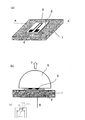
本発明の光素子の実施形態1を、その斜視図の図1(a)とA-A’断面図の図1(b)を用いて説明する。本実施形態では、基板1側から、所望の周波数特性を持つ電磁波結合構造体を含む複数の電極である電極兼アンテナ3と半導体層2との接合面に励起光6を照射できる構造となっている。このために、基板1は、半導体層2をエピタキシャル成長したときの基板ではなく、照射する励起光6に対して透明で波長分散の小さい材料の基板であり、ここに半導体層2が転写されている。つまり、半導体層2は、エピタキシャル層の成長基板を除去して別の基板1に転写されたところのエピタキシャル層である。ショットキー接合を構成する金属―半導体接触は、励起光6のフォトンエネルギーよりもバンドギャップが広い半導体層2の上に電極兼アンテナ3を形成することで実現している。ショットキー接合を形成する電極は、励起光6が照射される光照射面及びテラヘルツ波と結合する結合構造体を含み構成された電極兼アンテナ3となっている。この構成では、光照射面に達するまでの励起光6の透過領域は、半導体層2の領域及び励起光6の波長帯域において半導体層2よりも波長分散の小さい領域(基板1)のみを含むことになる。本実施形態では、電極兼アンテナ3の電磁波結合構造体は、発生したテラヘルツ波と結合して再放射するためのギャップ部を含む所望の周波数特性のアンテナであるが、電磁波結合構造体は、より一般的な結合構造体であってもよい。なお、図1(a)において、4は、電極兼アンテナ3にバイアス供給するための伝導線及びパッドである。
Hereinafter, embodiments and examples of the present invention will be described with reference to the drawings.
(Embodiment 1)
テラヘルツ波発生の原理について図2を用いて説明する。図2(a)は金属―半導体接触近傍のエネルギーバンド構造を示す。54が接合部であり、左側が金属(上記構造では電極兼アンテナ3)、右側が半導体(上記構造では半導体層2)を示している。50は金属のフェルミ準位であり、接合により半導体のフェルミ準位52と一致する様になっている。本説明図では、51、53はそれぞれ半導体の伝導帯、価電子帯を示しており、例えば半絶縁性の半導体によりフェルミ準位がほぼ中央にある場合が記載されている。また、金属の仕事関数Φmと半導体の仕事関数Φsが一致してフラットバンドを形成している場合が示されている。このとき、半導体の伝導帯51は金属のフェルミ準位50よりもq(Φm−χ)だけ高いエネルギー位置(qは素電荷)にあり、この差がショットキー障壁qΦbとなる。ここで、χは半導体の電子親和力であり、真空準位から伝導帯51までのエネルギー差を表す量である。理想的には、この様にして、ショットキー障壁が決まるが、実際には表面状態によりピンニングが起きるためΦbは小さくなる傾向があり、実測で求める必要がある。
The principle of terahertz wave generation will be described with reference to FIG. FIG. 2 (a) shows the energy band structure near the metal-semiconductor contact.
上記構成において、半導体側に陽極、金属に陰極を接続してバイアスすると、通常は、ショットキー障壁があるために電流は殆ど流れない。ここで、図2(b)に示す様に、ショットキー接合近傍に障壁高さqΦbよりも大きいフォトンエネルギーを持つ光55を照射すると、エネルギーを得た電子が光のフォトンエネルギー以下の障壁を越え、更に半導体に印加された電界により電子が加速される。このとき瞬時的な光照射を行えば、瞬時電流が流れてダイポールの変動が起こることで電磁波が発生する。光照射がフェムト秒オーダーの光パルスであれば、テラヘルツ帯にフーリエ周波数成分を含む様な電磁波パルスを発生させることができる。上述の光伝導素子と異なる点は、半導体のエネルギーバンドギャップ以上のフォトンエネルギーを持つ光の照射でフォトキャリアを得るのではなく、ショットキー障壁を越えるエネルギーを得た光電子を用いることである。従って、照射光55のフォトンエネルギーは半導体層のバンドギャップエネルギーよりも小さくてよく、その場合、照射光55は半導体層を透過できる。また、図2(b)の様な方向の電界印加では高抵抗を保つことができ、ブレークダウンが起こるまで高電界を印加することができる。これに対して、上述のInGaA光伝導素子では、抵抗が低いため、ブレークダウンが起こる前に電流が増加して印加電圧の大きさに制限があった。
In the above configuration, when the anode is connected to the semiconductor side and the cathode is connected to the metal and biased, normally, almost no current flows because of the Schottky barrier. Here, as shown in FIG. 2 (b), when light 55 having a photon energy larger than the barrier height qΦb is irradiated in the vicinity of the Schottky junction, the energy gained electron exceeds the barrier below the photon energy of the light. Furthermore, electrons are accelerated by the electric field applied to the semiconductor. If instantaneous light irradiation is performed at this time, an electromagnetic current is generated by an instantaneous current flowing and dipole fluctuation. If the light irradiation is a femtosecond order optical pulse, an electromagnetic wave pulse including a Fourier frequency component in the terahertz band can be generated. The difference from the above-described photoconductive element is not to obtain photocarriers by irradiating light having photon energy larger than the energy band gap of the semiconductor, but to use photoelectrons that have obtained energy exceeding the Schottky barrier. Therefore, the photon energy of the
半導体中を走行した電子は、半導体中で散乱などによりエネルギーを失えば電磁波が発生しなくなるが、典型的には縦光学フォノン散乱により数100fsec以下で消失する。この値は、通常の半導体においてキャリア再結合で消滅するキャリアの寿命に比べて十分短く、テラヘルツパルスを発生させることができる。上記構成において、光55の照射は一対の電極兼アンテナ3のうちの電子のエミッターとなる電極部分側に行う。このとき、ギャップ部を介した電極兼アンテナ3のもう一方の電極部分(ここには光照射を行わない)も同様のショットキー接合を形成する場合、ここの状態は図2(b)と反対のバイアス状態であるため、半導体層の伝導電子はこの電極部分に伝導できる。なお、このコレクタ側となる電極部分はショットキー接合を形成してもよいし、オーミック接合を形成してもよい。
Electrons that have traveled in a semiconductor lose their energy due to scattering or the like in the semiconductor and no longer generate electromagnetic waves, but typically disappear in a few hundred fsec or less due to longitudinal optical phonon scattering. This value is sufficiently shorter than the lifetime of carriers that disappear due to carrier recombination in a normal semiconductor, and a terahertz pulse can be generated. In the above configuration, the light 55 is irradiated on the side of the electrode portion of the pair of electrode /
この様にショットキー接合部近傍にフェムト秒オーダーの超短パルスを照射するとテラヘルツ波が発生する。このとき、一般的な光伝導素子と同様に電磁波発生部近傍にダイポールアンテナなどを設けると、発生した電磁波は一旦アンテナに結合し、アンテナ特性に従った指向性、周波数特性を示して、図1(b)の符号7で示す様な方向で空間に放射される。好適には、放射指向性を向上するために、図1(b)に示す様な高抵抗シリコンの超半球レンズ5などが用いられるが、これはなくてもよい。
In this manner, when an ultrashort pulse of femtosecond order is irradiated in the vicinity of the Schottky junction, a terahertz wave is generated. At this time, when a dipole antenna or the like is provided in the vicinity of the electromagnetic wave generation unit as in a general photoconductive element, the generated electromagnetic wave is once coupled to the antenna, and exhibits directivity and frequency characteristics according to the antenna characteristics. It is radiated into space in the direction indicated by
以上の説明ではフラットバンド型のタイプで説明したが、金属、半導体材料及びその導電型の組み合わせによって、様々なケースがあり得る。従って、ショットキー障壁が形成されるのであれば、これらも本実施形態の変形例として利用できる。例えば、同じ半導体材料を用いても、不純物ドープを行うことでそのフェルミ準位を変更でき、その仕事関数を変更可能であるので、ショットキー障壁の態様を所望に設計できる。また、正孔をキャリアとして用いる場合は、上記陽極と陰極を入れ替えればよい。ただし、正孔と電子は有効質量が異なるので、有効質量に応じて、金属―半導体接触近傍のエネルギーバンド構造を設計する必要がある。 In the above description, the flat band type has been described, but various cases may occur depending on the combination of metal, semiconductor material, and conductivity type. Therefore, if a Schottky barrier is formed, these can also be used as a modification of this embodiment. For example, even if the same semiconductor material is used, the Fermi level can be changed by doping impurities and the work function can be changed, so that the Schottky barrier mode can be designed as desired. When holes are used as carriers, the anode and the cathode may be exchanged. However, since holes and electrons have different effective masses, it is necessary to design an energy band structure near the metal-semiconductor contact according to the effective mass.
本実施形態によれば、ショットキー接合部の光照射領域を増大する構造を実現できて、光励起により効率良くテラヘルツ波を発生或いは検出することができる。特に、1μm以上の通信波長帯の励起光に対して有効な光素子であるテラヘルツ波発生・検出素子、及びそれを用いた計測装置、イメージング装置などを提供することができる。この場合、ファイバを用いた励起レーザを照射手段とできるので、装置の小型化、低コスト化が可能となる。また、電極を薄くして光透過性を大きくすることでショットキー接合部の光照射領域を増大する様なことが必要ないので、電気抵抗が高くなってテラヘルツ波の損失が大きくなるといったことも無くせる。 According to this embodiment, a structure that increases the light irradiation region of the Schottky junction can be realized, and terahertz waves can be efficiently generated or detected by light excitation. In particular, it is possible to provide a terahertz wave generation / detection element that is an effective optical element for excitation light in a communication wavelength band of 1 μm or more, a measurement device, an imaging device, and the like using the terahertz wave generation / detection device. In this case, since the excitation laser using the fiber can be used as the irradiation means, the apparatus can be reduced in size and cost. In addition, it is not necessary to increase the light irradiation area of the Schottky junction by thinning the electrode and increasing the light transmittance, so that the electrical resistance increases and the loss of terahertz waves increases. It can be lost.
(実施例1)
実施形態1に対応した実施例1について説明する。本実施例の構成は、基本的に実施形態1と同じである。本実施例では、図1に示す構成で、基板1は、照射レーザ光に対して透明で波長分散が小さい材料が望ましく、一般に石英やサファイヤ、樹脂などを用いることができる。光入射側の基板1の面には無反射コーティングなどを備えてもよい(不図示)。半導体層2としては、半絶縁性のInPを用い、電極兼アンテナ3はAu/Ti膜の蒸着などで形成することができる。この材料の組み合わせの場合、Auの仕事関数が約5.1eV、Tiの仕事関数が約4.3eV、InPの電子親和力が4.4eVである。InPのエネルギーバンドギャップは1.35eVであるため、半絶縁性の場合、そのフェルミ準位は伝導帯から1.35/2≒0.68eVだけ低いところとなり、Auのフェルミ準位とほぼ一致する。そのため、図2に示す様なフラットバンドを形成できると考えられる。実際には、Au/TiとInPのショットキー障壁高さはおよそ0.5eVという実測例があり、ショットキー接合部の伝導帯は湾曲する。ここでも、光照射面に達するまでの光6の透過領域は、半導体層2の領域及び光6の波長帯域において半導体層2よりも波長分散が小さい領域(石英などの基板1)のみを含む。
Example 1
Example 1 corresponding to
ショットキー障壁高さ及びInPのエネルギーギャップに相当するフォトンエネルギーを持つ光の波長は、それぞれ略2.4μm、0.91μmである。そこで、例えば1.55μm帯の通信波長帯のファイバ型フェムト秒レーザを用いれば、ショットキー接合部では光電子が励起されつつ半導体層2では励起されないという本発明の要件を満たすことができる。このため、システムの小型化、低コスト化の実現にも好適である。本実施例において、電極兼アンテナ3のアンテナ形状は、図1(c)に示す様に、ギャップ部を5μm、アンテナ長を15μm、幅を10μmとしたが、これに限るものではない。半絶縁性のInP膜の半導体層2は、Feドープ、厚さ1μmである。このInP膜は、InGaAs犠牲層を挟んだInP基板上のエピタキシャル膜をエピタキシャル転写技術により基板1に移設したものである。石英などの保持基板1への接着は、直接接合や接着剤を用いた方法で実現している。なお、半絶縁性InP基板を保持基板1と接合した後、研磨などにより薄膜を残す様にすれば、エピタキシャル層を成膜せずに半導体層2を作成することもできる。
The wavelengths of light having photon energy corresponding to the Schottky barrier height and the InP energy gap are approximately 2.4 μm and 0.91 μm, respectively. Thus, for example, if a fiber type femtosecond laser having a communication wavelength band of 1.55 μm is used, the requirement of the present invention that photoelectrons are excited in the Schottky junction but not in the
電極兼アンテナ3の片方の電極部分をオーミック接合にしたい場合には、電極領域に不純物を拡散させたり、AuGe/Ni/Au電極でアロイ化させたり、n-InGaAsエピタキシャル層を選択的に電極下部に設けたりするなどの方法(不図示)がある。また、図1では半導体層2のサイズが基板1のサイズより小さいものとなっているが、同形になっていても構わないし、電極兼アンテナ3のアンテナのある部分のみに半導体層2を形成してもよい。
When one electrode part of the electrode /
基板2がInP基板である場合、波長分散があるため、基板側から励起光の入射を行っても所望の狭いパルス幅が得られない可能性がある。しかし、本実施例は基板2側からの光入射に適した構造になっており、ショットキー接合を形成する電極―半導体接触の接合面の広い領域に光照射することができる。そのため、高効率なテラヘルツパルスの発生及び検出が可能である。その他の点は、実施形態1と同じである。
When the
(実施形態2)
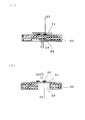
本発明の実施形態2を説明する。本実施形態では、図3(a)に示す様に、電極兼アンテナ22側が保持基板20に接着され、半導体膜21は、エピタキシャル成長時に使用した半導体を除去して保持基板20に転写されている。バイアスするための電極配線を基板20の表面に形成しておくことで、半導体層21表面の電極兼アンテナ22はこの電極配線に電気的にコンタクトする様に接着すればよいことになる。本構造では、保持基板20として、テラヘルツ波の透過性の良い高抵抗シリコンや石英、オレフィン・テフロン(登録商標)・ポリエチレンなどの樹脂が好適に用いられる。ここでは、励起レーザ光23は、電極22のない側から半導体膜21に入射され、実施形態1と同様の材料を半導体膜21に用いて、同じ原理でテラヘルツパルス24が発生し放射される。保持基板20は、テラヘルツ波放射の指向性を向上するために、レンズ形状にしたり或いはレンズを別途備えたりしてもよい。本実施形態では、光照射面に達するまでの励起レーザ光23の透過領域は、半導体層21の領域のみを含む。
(Embodiment 2)
A second embodiment of the present invention will be described. In this embodiment, as shown in FIG. 3A, the electrode /
本実施形態によれば、励起光23が薄い半導体膜21のみを透過してショットキー接合部に照射されるため、分散の影響を受けずにバンド幅の広い状態の光を照射でき、テラヘルツ波の帯域を伸ばすことができる。その他の点は、実施形態1と同じである。
According to the present embodiment, since the excitation light 23 passes only through the
(実施形態3)
本発明の実施形態3を説明する。本実施形態では、図3(b)に示す様に、保持基板30の一部に穴33を開けて、励起レーザ光34が半導体層31を介して電極兼アンテナ32と半導体層31とのショットキー接合部に直接入射できる様になっている。本素子では、基板は、穴付きの保持基板30であればよく、絶縁性基板であったり、或いは絶縁層を介して半導体膜31に接する基板であったりする。ここでは、基板30の材料は問わない。従って、半導体膜31をエピタキシャル成長したときの基板をそのまま用いてもよい。本実施形態でも、光照射面に達するまでの励起レーザ光34の透過領域は、半導体層31の領域のみを含む。
(Embodiment 3)
穴加工をする場合には、半導体基板と半導体層31との間にエッチングストップ層を設ければ制御性を向上することができる。例えば、InP系の場合には、InGaAsなどのエッチングストップ層が用いられる。本実施形態は、励起光34もテラヘルツ波も真空中または空気中を伝搬し、物質中を殆ど透過しない構造のため、材料の波長分散の影響を殆ど受けない。その他の点は、実施形態1と同じである。
In the case of drilling, controllability can be improved by providing an etching stop layer between the semiconductor substrate and the
(実施形態4)
本発明の実施形態4を説明する。本実施形態では、図4に示す様に、電極である電極兼アンテナ42、43が半導体層である半導体膜41の上面と下面に形成され、電極のギャップ部が半導体膜41の膜厚で規定されている。保持基板40の表面に一方の電極ライン43が設けられ、ここに半導体膜41が実施形態1と同様に転写され、更にその表面に、アンテナを兼ねる他方の電極ライン42が形成されている。この場合、例えば、電極ライン43と並行して伸びる電極ライン42などがアンテナとして機能する様に設計される。
(Embodiment 4)
Embodiment 4 of the present invention will be described. In the present embodiment, as shown in FIG. 4, the electrode and
本実施形態では、励起レーザ光44は、図4(a)に示す様に、電極兼アンテナ42、43で挟まれた半導体膜41の端部の側端面より入射する。つまり、励起レーザ光44の光照射面が、半導体膜41の端部にある電極との接合面に位置している。基板40としてオレフィンなどの樹脂を用いれば、半導体膜41は光の吸収が小さく且つその屈折率が樹脂基板40より高いため、空気と樹脂とに挟まれた半導体膜41が、電極兼アンテナ42、43との接合面に沿って伸びるスラブ導波路として機能する。よって、半導体膜41の側端面に入射した励起レーザ光44は、このスラブ導波路を伝搬しながら、ショットキー接合における光電子を高効率に生成することができる。実施形態1と同様に、テラヘルツ波46の指向性を向上するために高抵抗シリコンの超半球レンズ45を備えてもよい。その他の点は、実施形態1と同じである。
In the present embodiment, the
(実施形態5)
テラヘルツ時間領域分光システム(THz−TDS)に係る実施形態5を図5に沿って説明する。ここでは、本発明の光素子と光源と光学手段を含む光装置をテラヘルツパルス発生手段として用いて時間領域分光装置を構築した。この様な分光システム自体は、公知のものと基本的に同じである。この分光システムは、光源である短パルスレーザ830と、ハーフミラー910と、遅延部である光遅延系920と、電磁波発生素子800と、電磁波検出素子940とを主要な要素として備えている。ハーフミラー910で分割されたポンプ光931とプローブ光932は、それぞれ、光学手段であるレンズ990、980を介して電磁波発生素子800と電磁波検出素子940を照射する。ここで、800は本発明による光素子であり、レンズ990を介したポンプ光931がショットキー接合を持つ電極の光照射面に照射される様な電磁波発生素子を構成している。遅延部は、電磁波発生素子800におけるテラヘルツ波発生時と電磁波検出素子940におけるテラヘルツ波検出時との間の遅延時間を調整できれば、どの様なものでもよい。
(Embodiment 5)
電圧源820により電圧が印加されている電磁波発生素子800から発生したテラヘルツ波は、テラヘルツ波ガイド933、935によって検体950に導かれる。検体950の吸収スペクトルなどの情報を含むテラヘルツ波は、テラヘルツ波ガイド934、936によって導かれて電磁波検出素子940で検出される。ここでは、電磁波検出素子940は従来型のLT-GaAsによる光伝導素子であり、これに接続された電流計960の検出電流の値は、検出されたテラヘルツ波の振幅に比例する。時間分解を行う(つまり電磁波の時間波形を取得する)ためには、プローブ光932側の光路長を変化させる光遅延系920を動かすなどして、ポンプ光931とプローブ光932との照射タイミングを制御すればよい。
The terahertz wave generated from the electromagnetic
本実施形態では、励起レーザ光源830として1.5μm帯ファイバ型フェムト秒レーザを用い、本発明の発生素子800として、半絶縁性InPとAu/Tiとによるショットキー接合を用いる実施例1の素子などを用いる。検出側は、部品点数は増えるが、プローブ光932側に第二次高調波発生器(SHG結晶)970を挿入し、電磁波検出素子940として低温成長GaAsによる光伝導素子を用いると、信号雑音比が向上して好ましい。この様に、本発明の光装置であるテラヘルツパルス発生手段を用いてテラヘルツ時間領域分光システムを構成することが可能である。また、本発明の光素子と光源と光学手段を含む光装置をテラヘルツパルス検出手段として用いて時間領域分光装置を構築することもできる。
In this embodiment, a 1.5 μm band fiber type femtosecond laser is used as the excitation
(実施例2)
実施形態5に対応した実施例2について説明する。本実施例では、本発明による電磁波発生素子800には20Vの電圧を印加し、ポンプ光931として、波長1.56μmのファイバーレーザ830からパルス幅30fsec、平均パワー20mWの超短パルス光を照射する。検出側では、パワー5mWのプローブ光932を照射して検出した電流を、107程度の増幅率と帯域10kHzを持つトランスインピーダンスアンプで電圧信号に変換し、必要に応じてフィルターを挿入する。これにより、典型的には、100mV前後のピークを持つテラヘルツパルスが観測される。プローブ光932の光路長を遅延ステージ920で変調することで、発生しているテラヘルツ波パルスの時間波形をサンプリングの原理により測定できる。得られた時間波形をフーリエ変換することで、5THzを越える帯域のスペクトルが得られる。これらの駆動条件は一例であり、電磁波発生素子800への印加電圧、照射光パワーは上記の値に限るものではない。また、電磁波発生素子800の印加電圧を10kHzで変調、或いは光チョッパーを用いて光強度を変調させ、ロックインアンプによる検波で信号検出してもよい。
(Example 2)
Example 2 corresponding to
(実施形態6)
これまで、本発明の光素子は主にテラヘルツ波発生素子として説明してきたが、検出素子として使用することも可能である。検出素子は、例えば、実施形態1の説明で用いた図1で示す構成と全く同じ構成を有し、テラヘルツ波7の伝搬方向が素子に向けられる構成になる。テラヘルツ波検出の原理は次の通りである。励起光6の照射によりエネルギーを得た電子が、入力するテラヘルツ波7の電界によって生じた障壁を越え、半導体層2中を走行する。これにより、電極間に電流が流れ、この電流を検出することによりテラヘルツ波の電界強度を検出できる。ここでは、テラヘルツ波7は電極兼アンテナ3に結合して効率良く取り込まれ、励起光6は効率良くエネルギーを電子に与える。
(Embodiment 6)
So far, the optical element of the present invention has been mainly described as a terahertz wave generating element, but it can also be used as a detecting element. For example, the detection element has the same configuration as that shown in FIG. 1 used in the description of the first embodiment, and the propagation direction of the
つまり、前記光照射面に光6が照射されたタイミングでは光電子が励起されており、テラヘルツ波7による電界が印加されると、その極性によっては図2(b)の様なエネルギーバンド構造になる。これにより、光電子が流れることでテラヘルツ波7による電界を検出できる。ただし、光伝導素子の様に両極性ではないため、出力波形の解析には、予め得ておいた検量線などのデータを用いて補正が必要になる。
In other words, photoelectrons are excited at the timing when the light irradiation surface is irradiated with the
1‥基板、2‥半導体層、3‥電極兼アンテナ(電極、結合構造体)、6‥励起光、7‥テラヘルツ波
DESCRIPTION OF
Claims (11)
前記光のフォトンエネルギーよりも大きいエネルギーバンドギャップを持つ半導体層と、前記半導体層と電気的に接触して形成された複数の電極と、を備え、
前記電極のうち少なくとも1つは、前記半導体層との間に前記光のフォトンエネルギー以下の障壁高さを持つショットキー接合を形成し、
前記ショットキー接合を形成する電極と前記半導体層との接合面の少なくとも一部は、前記電極の形成されていない半導体層の面を透過した前記光が照射される光照射面を含むことを特徴とする光素子。 An optical element that generates or detects terahertz waves by light irradiation,
A semiconductor layer having an energy band gap larger than the photon energy of the light, and a plurality of electrodes formed in electrical contact with the semiconductor layer,
At least one of the electrodes forms a Schottky junction with the semiconductor layer having a barrier height equal to or lower than the photon energy of the light,
At least a part of the bonding surface between the electrode forming the Schottky junction and the semiconductor layer includes a light irradiation surface irradiated with the light transmitted through the surface of the semiconductor layer where the electrode is not formed. An optical element.
請求項1から7のいずれか1項に記載の光素子と、前記光素子を励起するための光を出力する光源と、前記光素子の前記電極の形成されていない半導体層の面を透過して前記光照射面に前記光源の光を照射するための光学手段と、を有することを特徴とする光装置。 An optical device that generates or detects terahertz waves,
The optical element according to any one of claims 1 to 7, a light source that outputs light for exciting the optical element, and a surface of the semiconductor layer on which the electrode of the optical element is not formed. And an optical means for irradiating the light irradiation surface with light from the light source.
レーザー光を発生するレーザー光源と、
前記レーザー光が照射されたときに前記テラヘルツ波を発生または検出する光素子と、
前記レーザー光源から前記光素子へ前記レーザー光を導く光学手段と、
を有し、
前記光素子は、半導体層と、前記半導体層と電気的に接触して形成されている複数の電極と、を有し、
前記複数の電極のうちの少なくとも1つは、該1つの電極と前記半導体層との間にショットキー接合を形成し、
前記レーザー光源は、前記ショットキー接合の障壁高さより大きく前記半導体層のエネルギーバンドギャップより小さいフォトンエネルギーを持つレーザー光を発生し、
前記光学手段は、前記複数の電極の形成されていない前記半導体層の面を透過した前記レーザー光で前記ショットキー接合の部分を照射する様に配置されていることを特徴とする光装置。 An optical device that generates or detects terahertz waves,
And Relais Za source to generate a laser beam,
An optical element that generates or detects the terahertz wave when irradiated with the laser beam;
Optical means for guiding the laser light from the laser light source to the optical element;
Have
The optical element has a semiconductor layer and a plurality of electrodes formed in electrical contact with the semiconductor layer,
At least one of the plurality of electrodes forms a Schottky junction between the one electrode and the semiconductor layer;
The laser light source generates laser light having a photon energy larger than a barrier height of the Schottky junction and smaller than an energy band gap of the semiconductor layer;
Said optical means, the optical apparatus characterized by being arranged so as to irradiate the portion of the Schottky junction in the laser light transmitted through the surface of said semiconductor layer which is not formed of the plurality of electrodes.
前記発生手段から放射され検体を経て来たテラヘルツ波を検出するための検出手段と、
前記発生手段におけるテラヘルツ波発生時と前記検出手段におけるテラヘルツ波検出時との間の遅延時間を調整するための遅延部と、
を備えたテラヘルツ時間領域分光装置であって、
前記発生手段と前記検出手段の少なくとも一方が、請求項8から10のいずれか1項に記載の光装置であることを特徴とする装置。 Generating means for generating terahertz waves;
Detection means for detecting terahertz waves radiated from the generation means and passed through the specimen;
A delay unit for adjusting a delay time between terahertz wave generation in the generation unit and terahertz wave detection in the detection unit;
A terahertz time domain spectroscopic device comprising:
The apparatus according to claim 8, wherein at least one of the generating means and the detecting means is the optical device according to claim 8.
Priority Applications (6)
| Application Number | Priority Date | Filing Date | Title |
|---|---|---|---|
| JP2010044838A JP5654760B2 (en) | 2010-03-02 | 2010-03-02 | Optical element |
| EP20110153651 EP2363893A2 (en) | 2010-03-02 | 2011-02-08 | Optical element, optical device and terahertz time-domain spectroscopic apparatus including the same |
| US13/031,014 US8759771B2 (en) | 2010-03-02 | 2011-02-18 | Optical element, and optical device and terahertz time-domain spectroscopic apparatus including the same |
| RU2011107929/28A RU2462790C1 (en) | 2010-03-02 | 2011-03-01 | Optical element, optical device and terahertz spectroscopic device with time resolution, including said device |
| CN201110049029.5A CN102194914B (en) | 2010-03-02 | 2011-03-02 | Optical element, optical device and terahertz time-domain spectroscopic apparatus including the same |
| KR20110018327A KR101385166B1 (en) | 2010-03-02 | 2011-03-02 | Optical element, and optical device and terahertz time-domain spectroscopic apparatus including the same |
Applications Claiming Priority (1)
| Application Number | Priority Date | Filing Date | Title |
|---|---|---|---|
| JP2010044838A JP5654760B2 (en) | 2010-03-02 | 2010-03-02 | Optical element |
Publications (3)
| Publication Number | Publication Date |
|---|---|
| JP2011181708A JP2011181708A (en) | 2011-09-15 |
| JP2011181708A5 JP2011181708A5 (en) | 2014-04-03 |
| JP5654760B2 true JP5654760B2 (en) | 2015-01-14 |
Family
ID=44227209
Family Applications (1)
| Application Number | Title | Priority Date | Filing Date |
|---|---|---|---|
| JP2010044838A Expired - Fee Related JP5654760B2 (en) | 2010-03-02 | 2010-03-02 | Optical element |
Country Status (6)
| Country | Link |
|---|---|
| US (1) | US8759771B2 (en) |
| EP (1) | EP2363893A2 (en) |
| JP (1) | JP5654760B2 (en) |
| KR (1) | KR101385166B1 (en) |
| CN (1) | CN102194914B (en) |
| RU (1) | RU2462790C1 (en) |
Families Citing this family (12)
| Publication number | Priority date | Publication date | Assignee | Title |
|---|---|---|---|---|
| JP5506258B2 (en) * | 2008-08-06 | 2014-05-28 | キヤノン株式会社 | Rectifier element |
| JP2013076618A (en) * | 2011-09-30 | 2013-04-25 | Sony Corp | Photoconductive element, lens, terahertz emission microscope, and method for manufacturing device |
| RU2511070C1 (en) * | 2012-10-01 | 2014-04-10 | Общество с ограниченной ответственностью "ТИДЕКС" | Device for imaging terahertz radiation sources |
| JP2014241517A (en) * | 2013-06-11 | 2014-12-25 | キヤノン株式会社 | Device that generates terahertz wave and device that detects terahertz wave |
| JP2016192423A (en) * | 2015-03-30 | 2016-11-10 | パイオニア株式会社 | Photoconductive element and measurement device |
| EP3096180A1 (en) * | 2015-05-20 | 2016-11-23 | Philipps-Universität Marburg | Method for expanding the frequency spectrum of an electromagnetic wave and component for realizing the same |
| DE102015112408A1 (en) * | 2015-07-29 | 2017-02-02 | Endress + Hauser Gmbh + Co. Kg | Pressure sensor and method for monitoring a pressure sensor |
| JP6829517B2 (en) * | 2016-07-23 | 2021-02-10 | 国立大学法人千葉大学 | Infrared light element |
| RU2657306C2 (en) * | 2016-10-07 | 2018-06-13 | Федеральное государственное бюджетное учреждение науки Институт сверхвысокочастотной полупроводниковой электроники Российской академии наук (ИСВЧПЭ РАН) | Ingaas-based material on inp substrates for photo-conducting antennas |
| RU186068U1 (en) * | 2018-10-05 | 2018-12-28 | Федеральное государственное бюджетное учреждение науки Институт физики твердого тела Российской академии наук (ИФТТ РАН) | Sapphire cell for intra-wave terahertz spectroscopy |
| DE102019135487A1 (en) * | 2019-12-20 | 2021-06-24 | Helmut Fischer GmbH Institut für Elektronik und Messtechnik | Device for transmitting and / or receiving terahertz radiation and use thereof |
| JP2020198448A (en) * | 2020-08-26 | 2020-12-10 | パイオニア株式会社 | Photoconductive element and measurement device |
Family Cites Families (14)
| Publication number | Priority date | Publication date | Assignee | Title |
|---|---|---|---|---|
| US5729017A (en) * | 1996-05-31 | 1998-03-17 | Lucent Technologies Inc. | Terahertz generators and detectors |
| US7619263B2 (en) * | 2003-04-08 | 2009-11-17 | Sensor Electronic Technology, Inc. | Method of radiation generation and manipulation |
| JP4794878B2 (en) * | 2004-03-26 | 2011-10-19 | キヤノン株式会社 | Photoconductive element |
| US7615787B2 (en) * | 2004-03-26 | 2009-11-10 | Canon Kabushiki Kaisha | Photo-semiconductor device and method of manufacturing the same |
| CN1993869A (en) | 2004-07-30 | 2007-07-04 | 佳能株式会社 | Optical semiconductor device |
| JP2006086227A (en) | 2004-09-14 | 2006-03-30 | Osaka Univ | Optical switch |
| JP4481946B2 (en) | 2006-03-17 | 2010-06-16 | キヤノン株式会社 | Detection element and image forming apparatus |
| JP4709059B2 (en) | 2006-04-28 | 2011-06-22 | キヤノン株式会社 | Inspection apparatus and inspection method |
| RU2325729C1 (en) * | 2006-10-17 | 2008-05-27 | Государственное образовательное учреждение высшего профессионального образования "Российский университет дружбы народов" (РУДН) | Uncooled metallic bolometer |
| KR101282775B1 (en) * | 2006-11-03 | 2013-07-05 | 엘지이노텍 주식회사 | Light emitting device having vertical topoloty and method of making the same |
| US8067739B2 (en) * | 2007-06-22 | 2011-11-29 | Canon Kabushiki Kaisha | Photoconductive element for generation and detection of terahertz wave |
| JP2010045157A (en) | 2008-08-12 | 2010-02-25 | Kansai Electric Power Co Inc:The | Terahertz electromagnetic wave radiation element and terahertz electromagnetic wave generation method |
| JP5419411B2 (en) * | 2008-10-08 | 2014-02-19 | キヤノン株式会社 | Terahertz wave generator |
| US8093139B2 (en) * | 2008-12-11 | 2012-01-10 | Anteos, Inc. | Method for fabrication of aligned nanowire structures in semiconductor materials for electronic, optoelectronic, photonic and plasmonic devices |
-
2010
- 2010-03-02 JP JP2010044838A patent/JP5654760B2/en not_active Expired - Fee Related
-
2011
- 2011-02-08 EP EP20110153651 patent/EP2363893A2/en not_active Withdrawn
- 2011-02-18 US US13/031,014 patent/US8759771B2/en not_active Expired - Fee Related
- 2011-03-01 RU RU2011107929/28A patent/RU2462790C1/en not_active IP Right Cessation
- 2011-03-02 CN CN201110049029.5A patent/CN102194914B/en not_active Expired - Fee Related
- 2011-03-02 KR KR20110018327A patent/KR101385166B1/en not_active IP Right Cessation
Also Published As
| Publication number | Publication date |
|---|---|
| KR101385166B1 (en) | 2014-04-29 |
| KR20110099649A (en) | 2011-09-08 |
| CN102194914A (en) | 2011-09-21 |
| EP2363893A2 (en) | 2011-09-07 |
| CN102194914B (en) | 2014-04-16 |
| US20110215245A1 (en) | 2011-09-08 |
| US8759771B2 (en) | 2014-06-24 |
| RU2462790C1 (en) | 2012-09-27 |
| JP2011181708A (en) | 2011-09-15 |
Similar Documents
| Publication | Publication Date | Title |
|---|---|---|
| JP5654760B2 (en) | Optical element | |
| Burford et al. | Review of terahertz photoconductive antenna technology | |
| JP6062640B2 (en) | Photoconductive element | |
| US8405031B2 (en) | Terahertz wave generator | |
| JP5178398B2 (en) | Photoconductive element | |
| JP5656428B2 (en) | Photoconductive element | |
| US7498593B2 (en) | Terahertz radiation sources and methods | |
| US8481939B2 (en) | Photoconductive device, and terahertz wave generation and detection apparatuses each using the photoconductive device | |
| JP5582822B2 (en) | Electromagnetic wave generator | |
| US8766188B2 (en) | Photoconductive element | |
| JP4975000B2 (en) | Electromagnetic wave generating element, electromagnetic wave integrated element, and electromagnetic wave detecting device | |
| Khiabani | Modelling, design and characterisation of terahertz photoconductive antennas | |
| US9224899B2 (en) | Light mixer for generating terahertz radiation | |
| Peytavit et al. | THz photomixers | |
| JP2010050287A (en) | Photoconductive element | |
| Lavrukhin et al. | Emission efficiency of terahertz antennas with conventional topology and metal metasurface: a comparative analysis | |
| JP2015148541A (en) | Light conduction antenna, camera, imaging apparatus and measurement apparatus | |
| JP5737956B2 (en) | Terahertz wave device | |
| Nandi | ErAs: In (Al) GaAs photoconductors for 1550 nm-based Terahertz time domain spectroscopy systems | |
| KR102098284B1 (en) | Non-contact measuring system for optoelectronic properties of semiconductor material | |
| Moon et al. | Field enhancement effect in nano-electrodes for THz generation and detection | |
| JP2021184488A (en) | Photoconductive element and measurement device | |
| Wang | High Sensitivity Terahertz Receivers Based on Plasmonic Photoconductors. |
Legal Events
| Date | Code | Title | Description |
|---|---|---|---|
| A621 | Written request for application examination |
Free format text: JAPANESE INTERMEDIATE CODE: A621 Effective date: 20130304 |
|
| A521 | Request for written amendment filed |
Free format text: JAPANESE INTERMEDIATE CODE: A523 Effective date: 20140218 |
|
| A131 | Notification of reasons for refusal |
Free format text: JAPANESE INTERMEDIATE CODE: A131 Effective date: 20140313 |
|
| A521 | Request for written amendment filed |
Free format text: JAPANESE INTERMEDIATE CODE: A523 Effective date: 20140430 |
|
| TRDD | Decision of grant or rejection written | ||
| A01 | Written decision to grant a patent or to grant a registration (utility model) |
Free format text: JAPANESE INTERMEDIATE CODE: A01 Effective date: 20141023 |
|
| A61 | First payment of annual fees (during grant procedure) |
Free format text: JAPANESE INTERMEDIATE CODE: A61 Effective date: 20141121 |
|
| LAPS | Cancellation because of no payment of annual fees |