JP5651502B2 - Method for producing functional film - Google Patents
Method for producing functional film Download PDFInfo
- Publication number
- JP5651502B2 JP5651502B2 JP2011050108A JP2011050108A JP5651502B2 JP 5651502 B2 JP5651502 B2 JP 5651502B2 JP 2011050108 A JP2011050108 A JP 2011050108A JP 2011050108 A JP2011050108 A JP 2011050108A JP 5651502 B2 JP5651502 B2 JP 5651502B2
- Authority
- JP
- Japan
- Prior art keywords
- film
- electrode
- substrate
- forming
- film formation
- Prior art date
- Legal status (The legal status is an assumption and is not a legal conclusion. Google has not performed a legal analysis and makes no representation as to the accuracy of the status listed.)
- Expired - Fee Related
Links
Images


Classifications
-
- C—CHEMISTRY; METALLURGY
- C23—COATING METALLIC MATERIAL; COATING MATERIAL WITH METALLIC MATERIAL; CHEMICAL SURFACE TREATMENT; DIFFUSION TREATMENT OF METALLIC MATERIAL; COATING BY VACUUM EVAPORATION, BY SPUTTERING, BY ION IMPLANTATION OR BY CHEMICAL VAPOUR DEPOSITION, IN GENERAL; INHIBITING CORROSION OF METALLIC MATERIAL OR INCRUSTATION IN GENERAL
- C23C—COATING METALLIC MATERIAL; COATING MATERIAL WITH METALLIC MATERIAL; SURFACE TREATMENT OF METALLIC MATERIAL BY DIFFUSION INTO THE SURFACE, BY CHEMICAL CONVERSION OR SUBSTITUTION; COATING BY VACUUM EVAPORATION, BY SPUTTERING, BY ION IMPLANTATION OR BY CHEMICAL VAPOUR DEPOSITION, IN GENERAL
- C23C16/00—Chemical coating by decomposition of gaseous compounds, without leaving reaction products of surface material in the coating, i.e. chemical vapour deposition [CVD] processes
- C23C16/44—Chemical coating by decomposition of gaseous compounds, without leaving reaction products of surface material in the coating, i.e. chemical vapour deposition [CVD] processes characterised by the method of coating
- C23C16/4401—Means for minimising impurities, e.g. dust, moisture or residual gas, in the reaction chamber
- C23C16/4408—Means for minimising impurities, e.g. dust, moisture or residual gas, in the reaction chamber by purging residual gases from the reaction chamber or gas lines
-
- C—CHEMISTRY; METALLURGY
- C23—COATING METALLIC MATERIAL; COATING MATERIAL WITH METALLIC MATERIAL; CHEMICAL SURFACE TREATMENT; DIFFUSION TREATMENT OF METALLIC MATERIAL; COATING BY VACUUM EVAPORATION, BY SPUTTERING, BY ION IMPLANTATION OR BY CHEMICAL VAPOUR DEPOSITION, IN GENERAL; INHIBITING CORROSION OF METALLIC MATERIAL OR INCRUSTATION IN GENERAL
- C23C—COATING METALLIC MATERIAL; COATING MATERIAL WITH METALLIC MATERIAL; SURFACE TREATMENT OF METALLIC MATERIAL BY DIFFUSION INTO THE SURFACE, BY CHEMICAL CONVERSION OR SUBSTITUTION; COATING BY VACUUM EVAPORATION, BY SPUTTERING, BY ION IMPLANTATION OR BY CHEMICAL VAPOUR DEPOSITION, IN GENERAL
- C23C16/00—Chemical coating by decomposition of gaseous compounds, without leaving reaction products of surface material in the coating, i.e. chemical vapour deposition [CVD] processes
- C23C16/44—Chemical coating by decomposition of gaseous compounds, without leaving reaction products of surface material in the coating, i.e. chemical vapour deposition [CVD] processes characterised by the method of coating
- C23C16/50—Chemical coating by decomposition of gaseous compounds, without leaving reaction products of surface material in the coating, i.e. chemical vapour deposition [CVD] processes characterised by the method of coating using electric discharges
- C23C16/505—Chemical coating by decomposition of gaseous compounds, without leaving reaction products of surface material in the coating, i.e. chemical vapour deposition [CVD] processes characterised by the method of coating using electric discharges using radio frequency discharges
- C23C16/509—Chemical coating by decomposition of gaseous compounds, without leaving reaction products of surface material in the coating, i.e. chemical vapour deposition [CVD] processes characterised by the method of coating using electric discharges using radio frequency discharges using internal electrodes
-
- C—CHEMISTRY; METALLURGY
- C23—COATING METALLIC MATERIAL; COATING MATERIAL WITH METALLIC MATERIAL; CHEMICAL SURFACE TREATMENT; DIFFUSION TREATMENT OF METALLIC MATERIAL; COATING BY VACUUM EVAPORATION, BY SPUTTERING, BY ION IMPLANTATION OR BY CHEMICAL VAPOUR DEPOSITION, IN GENERAL; INHIBITING CORROSION OF METALLIC MATERIAL OR INCRUSTATION IN GENERAL
- C23C—COATING METALLIC MATERIAL; COATING MATERIAL WITH METALLIC MATERIAL; SURFACE TREATMENT OF METALLIC MATERIAL BY DIFFUSION INTO THE SURFACE, BY CHEMICAL CONVERSION OR SUBSTITUTION; COATING BY VACUUM EVAPORATION, BY SPUTTERING, BY ION IMPLANTATION OR BY CHEMICAL VAPOUR DEPOSITION, IN GENERAL
- C23C16/00—Chemical coating by decomposition of gaseous compounds, without leaving reaction products of surface material in the coating, i.e. chemical vapour deposition [CVD] processes
- C23C16/44—Chemical coating by decomposition of gaseous compounds, without leaving reaction products of surface material in the coating, i.e. chemical vapour deposition [CVD] processes characterised by the method of coating
- C23C16/54—Apparatus specially adapted for continuous coating
- C23C16/545—Apparatus specially adapted for continuous coating for coating elongated substrates
Landscapes
- Chemical & Material Sciences (AREA)
- Engineering & Computer Science (AREA)
- General Chemical & Material Sciences (AREA)
- Chemical Kinetics & Catalysis (AREA)
- Materials Engineering (AREA)
- Mechanical Engineering (AREA)
- Metallurgy (AREA)
- Organic Chemistry (AREA)
- Physics & Mathematics (AREA)
- Plasma & Fusion (AREA)
- Chemical Vapour Deposition (AREA)
Description
本発明は、長尺な基板を長手方向に搬送しつつ、プラズマCVDによって成膜を行なってガスバリアフィルム等の機能性フィルムを製造する製造方法に関する。 The present invention relates to a manufacturing method for manufacturing a functional film such as a gas barrier film by forming a film by plasma CVD while conveying a long substrate in the longitudinal direction.
光学素子、液晶ディスプレイや有機ELディスプレイなどの表示装置、半導体装置、薄膜太陽電池など、各種の装置に、ガスバリアフィルム、保護フィルム、光学フィルタや反射防止フィルム等の光学フィルムなど、各種の機能性フィルム(機能性シート)が利用されている。
これらの機能性フィルムの製造にプラズマCVDが利用されている。
Various functional films such as gas barrier films, protective films, optical films such as optical filters and antireflection films, etc. in various devices such as optical elements, display devices such as liquid crystal displays and organic EL displays, semiconductor devices, thin film solar cells, etc. (Functional sheet) is used.
Plasma CVD is used for the production of these functional films.
また、プラズマCVDに限らず、効率良く、高い生産性を確保して成膜を行なうためには、長尺な基板(ウェブ状の基板)を長手方向に搬送しつつ、連続的に成膜を行なうのが好ましい。
このような成膜方法を実施する装置として、長尺な基板をロール状に巻回してなる基板ロールから基板を送り出し、成膜済みの基板をロール状に巻回する、いわゆるロール・ツー・ロール(Roll to Roll(以下、RtoRともいう))の成膜装置が知られている。
このRtoRの成膜装置は、成膜位置を含む所定の経路で、基板ロールから巻取り軸まで所定の搬送経路で長尺な基板を通紙し(所定の搬送経路に基板を通し)、基板ロールからの基板の送り出しと、巻取り軸による成膜済の基板の巻取りとを同期して行いつつ、成膜位置において、長手方向に搬送される基板に連続的に成膜を行なう。
In addition to plasma CVD, in order to perform film formation efficiently and with high productivity, continuous film formation is performed while transporting a long substrate (web-like substrate) in the longitudinal direction. It is preferred to do so.
As an apparatus for carrying out such a film forming method, a so-called roll-to-roll process in which a substrate is fed from a substrate roll formed by winding a long substrate into a roll shape, and the film-formed substrate is wound into a roll shape. (Roll to Roll (hereinafter also referred to as RtoR)) film forming apparatuses are known.
This RtoR film forming apparatus passes a long substrate through a predetermined transport path from a substrate roll to a take-up shaft through a predetermined path including a film forming position (pass the substrate through the predetermined transport path), and the substrate. The film is continuously formed on the substrate transported in the longitudinal direction at the film forming position while the substrate feeding from the roll and the film winding of the substrate by the winding shaft are performed synchronously.
周知のように、プラズマCVD(容量結合型プラズマCVD)は、成膜される基板を挟んで、成膜電極と対向電極とからなる電極対を形成し、電極対の間に成膜ガス(プロセスガス)を供給すると共に、成膜電極に高周波電力等を供給することにより、プラズマを生成して、成膜を行うものである。
ここで、プラズマCVDによる成膜(気相堆積法による成膜)では、成膜系内において、基板以外の様々な場所に膜が付着/堆積してしまう。特に、成膜電極の表面(対向電極(基板)との対向面)には、大量の膜が付着してしまう。
As is well known, plasma CVD (capacitive coupling type plasma CVD) forms an electrode pair composed of a film-forming electrode and a counter electrode with a substrate to be formed in between, and a film-forming gas (process) between the electrode pair. Gas) and high-frequency power or the like to the film-forming electrode to generate plasma and form a film.
Here, in film formation by plasma CVD (film formation by a vapor deposition method), a film adheres / deposits at various places other than the substrate in the film formation system. In particular, a large amount of film adheres to the surface of the film forming electrode (the surface facing the counter electrode (substrate)).
成膜される基板(処理基板)を、順次、出し入れする、一般的な枚葉式(バッチ式)の成膜装置の場合には、成膜を終了したら、成膜ガスの代わりにクリーニングガスを成膜系内に導入し、成膜電極等に付着した膜を除去する。
しかしながら、生産性を向上するために、長時間、連続で成膜を行なうRtoRの装置では、非常に大量の膜が成膜電極に堆積してしまう。そのため、クリーニングガスを用いた成膜電極からの膜の除去には、多大な時間が必要となり、生産性を著しく低下してしまう結果となる。
In the case of a general single wafer type (batch type) film forming apparatus in which the substrate (processing substrate) to be formed is sequentially taken in and out, when the film formation is completed, a cleaning gas is used instead of the film forming gas. The film is introduced into the film forming system, and the film attached to the film forming electrode is removed.
However, in an RtoR apparatus that continuously forms films for a long time in order to improve productivity, a very large amount of film is deposited on the deposition electrodes. Therefore, it takes a lot of time to remove the film from the film-forming electrode using the cleaning gas, resulting in a significant reduction in productivity.
そのため、RtoRによる装置では、成膜電極等のクリーニング(清浄化)を迅速に行なうために、成膜電極や部品をとり外して、新しい物(クリーニング済の物)と交換し、膜が堆積した成膜電極等を、外部でクリーニングする方法が考えられる。 Therefore, in the RtoR apparatus, in order to quickly clean (clean) the film-forming electrodes, etc., the film-forming electrodes and parts are removed and replaced with new ones (cleaned ones), and the film is deposited. A method of cleaning the film forming electrode and the like outside is conceivable.
ところが、この方法では、成膜電極等の表面に大量の膜が堆積した状態で、成膜系(成膜空間)を大気解放する結果となる。そのため、大気解放の際に、成膜電極に付着していた大量の膜が、大気導入による急激な温度変化(熱応力)と、激しい気流とによって、成膜電極表面等に付着した膜が剥離し、かつ、いわゆるパーティクルとなって舞って、成膜系内全体に飛散/付着してしまう。
その結果、このパーティクルを除去するための成膜系内のクリーニングに、非常に多くの時間が必要になり、結果的に、やはり生産性を低下してしまう。
However, this method results in the film formation system (film formation space) being released to the atmosphere with a large amount of film deposited on the surface of the film formation electrode or the like. Therefore, a large amount of film attached to the film-forming electrode when released into the atmosphere is peeled off by the rapid temperature change (thermal stress) caused by the introduction of air and a strong air current. In addition, they act as so-called particles and are scattered / attached throughout the film forming system.
As a result, a very long time is required for cleaning the film forming system for removing the particles, and as a result, productivity is also lowered.
また、枚様式の成膜装置では、大気解放は、前述のようなクリーニングガスによるクリーニング後であり、かつ、大気解放時には、通常、成膜済の基板は、成膜系とは異なる空間に退避している。そのため、この大気解放時におけるパーティクルの飛散によって、製品となる成膜済の基板が汚染されることは無い。
これに対し、RtoRによる成膜装置では、通紙の手間等を考慮して、製品となる成膜済の基板が、成膜系内に存在した状態で、大気解放が行なわれる場合が多い。この際には、大気解放時に飛散したパーティクルが、成膜済の基板の表面や裏面に付着してしまい、これに起因して、成膜した膜の損傷や汚染等が生じ、製品の品質を低下してしまう。また、パーティクルが付着した状態で成膜済の基板を巻き取ると、隣接する基板(積層された基板)にパーティクルが当接し、また、付着して、成膜した膜の損傷や、製品の汚染など、製品品質を低下させる原因となってしまう。
In the single-layer film formation apparatus, the atmosphere is released after the cleaning with the cleaning gas as described above, and when the atmosphere is released, the film-formed substrate is usually retreated in a space different from the film formation system. doing. Therefore, the film-formed substrate that is the product is not contaminated by the scattering of the particles when the atmosphere is released.
On the other hand, in the film forming apparatus using RtoR, in consideration of the labor of paper passing, etc., air release is often performed in a state where a film-formed substrate as a product exists in the film forming system. At this time, particles scattered when released to the atmosphere adhere to the front and back surfaces of the substrate on which the film has been formed, resulting in damage and contamination of the film that has been formed. It will decline. In addition, when a film-formed substrate is taken up with particles attached, the particles come into contact with the adjacent substrate (laminated substrate) and adhere to the film, resulting in damage to the formed film or product contamination. It will cause the product quality to deteriorate.
同じRtoRの成膜装置でも、スパッタリング装置では、原理的に膜の付着力が高く、また、ガス同士の反応による成膜でも無いので、カソード等への膜の堆積位置も限られている。そのため、このような大気解放における膜の剥離やパーティクルの飛散の問題は、生じない。
しかしながら、プラズマCVDによる膜は、スパッタリングほど密着力は強くなく、しかも、特に成膜電極の表面には、全面的に、大量の膜が付着/堆積してしまう。そのため、このような成膜電極に堆積した膜の剥離、および、パーティクルの飛散を防止することは、困難である。
Even with the same RtoR film forming apparatus, the sputtering apparatus has high film adhesion in principle, and since there is no film formation by reaction between gases, the deposition position of the film on the cathode or the like is limited. Therefore, the problem of film peeling and particle scattering in such air release does not occur.
However, the film formed by plasma CVD does not have as strong an adhesive force as sputtering, and a large amount of film adheres / deposits on the entire surface of the film-forming electrode. Therefore, it is difficult to prevent peeling of the film deposited on such a film-forming electrode and scattering of particles.
また、前述のように、成膜電極等に付着/堆積した膜が剥離し、パーティクルとなる理由としては、昇温した部材が大気導入によって急速に冷却され、部材と膜との熱応力の差に起因して膜が剥離する点が挙げられる。
この熱応力に起因する膜の剥離を防止するために、温水やチラー等で成膜基板を温度調整して、大気開放を行なうことも可能ではある。しかしながら、プラズマCVDの成膜電極は、数百℃程度の高温となる。そのため、大気導入時に、成膜電極を、この温度に維持することは、生産性の点でも、安全性の点でも、非常に困難である。
In addition, as described above, the film adhered / deposited on the film forming electrode or the like peels off and becomes particles. The reason for this is that the heated member is rapidly cooled by the introduction of the air, and the difference in thermal stress between the member and the film. The film peels off due to the above.
In order to prevent peeling of the film due to the thermal stress, it is also possible to open the atmosphere by adjusting the temperature of the deposition substrate with hot water, a chiller or the like. However, plasma CVD film-forming electrodes are at a high temperature of about several hundred degrees Celsius. Therefore, it is very difficult to maintain the film-forming electrode at this temperature when introduced into the atmosphere, both in terms of productivity and safety.
さらに、成膜電極等に付着/堆積した膜の剥離、成膜系内でのパーティクルの飛散を防止するために、気流の急激な変化を与えないように、大気開放時における成膜系への大気導入を極めて低速で行なう、いわゆるスローベント機構を用いることも可能である。
しかしながら、最終的には、成膜基板等の温度変化による膜の剥離が発生してしまう。さらに、スローベント機構を用いると、成膜終了から、成膜系の大気解放までに、非常に長い時間がかかってしまうため、結果的に、やはり生産性を低下してしまう。
Furthermore, in order to prevent peeling of the film adhering / deposited on the film forming electrode, etc., and scattering of particles in the film forming system, the film forming system should be connected to the film forming system when it is opened to the atmosphere so as not to give a sudden change of air flow It is also possible to use a so-called slow vent mechanism that introduces the air at a very low speed.
However, finally, the film is peeled off due to the temperature change of the film formation substrate or the like. Further, when the slow vent mechanism is used, it takes a very long time from the completion of the film formation to the release of the film formation system into the atmosphere, and as a result, the productivity is also lowered.
本発明の目的は、前記従来技術の問題点を解決することにあり、RtoRを利用してプラズマCVDによって成膜を行なう機能性フィルムの製造において、成膜を停止(終了)した後の、成膜系の大気開放時に、成膜電極に付着/堆積した膜が剥離して、パーティクルとなって成膜系中に舞って、成膜系内の全域に付着/汚染することを防止できる、機能性フィルムの製造方法を提供することにある。 An object of the present invention is to solve the above-described problems of the prior art, and in the production of a functional film that is formed by plasma CVD using RtoR, the formation after the film formation is stopped (terminated). Function that prevents the film adhering / depositing on the film forming electrode from peeling off and moving into the film forming system and adhering / contaminating the entire area of the film forming system when the film system is opened to the atmosphere It is in providing the manufacturing method of an adhesive film.
前記目的を達成するために、本発明の機能性フィルムの製造方法は、長尺な基板を長手方向に搬送しつつ、プラズマCVDによって前記基板の表面に成膜を行うと共に、前記基板への成膜を停止して成膜系内を大気解放する際に、前記プラズマCVDによる成膜を行なうための成膜電極の表面が、前記成膜系内に露出していない状態とした後に、前記大気解放を行なうための気体を成膜系内に導入することを特徴とする機能性フィルムの製造方法を提供する。 In order to achieve the above object, the method for producing a functional film of the present invention forms a film on the surface of the substrate by plasma CVD while conveying a long substrate in the longitudinal direction, and forms the substrate on the substrate. When the film is stopped and the inside of the film forming system is released to the atmosphere, the surface of the film forming electrode for performing film formation by plasma CVD is not exposed in the film forming system, Provided is a method for producing a functional film, wherein a gas for releasing is introduced into a film forming system.
このような本発明の機能性フィルムの製造方法において、前記成膜電極の表面を所定のカバーで覆うことにより、前記成膜電極の表面が成膜系内に露出していない状態とするのが好ましい。また、前記カバーが、前記成膜電極の表面全面に当接して、前記成膜電極の表面を覆う形状を有するのが好ましい。また、前記カバーを移動して、前記成膜電極と、この成膜電極と電極対を成す対向電極との間に挿入した後、前記成膜電極を移動することにより、前記成膜電極の表面をカバーで覆うのが好ましい。
また、前記成膜電極の表面と、この成膜電極と電極対を成す対向電極の表面とが、互いに全面的に接触可能な形状を有し、前記成膜電極の表面を対向電極の表面に当接することにより、前記成膜電極の表面が成膜系内に露出していない状態とするのが好ましい。また、前記成膜電極を移動することにより、前記成膜電極の表面を対向電極の表面に当接するのが好ましい。
さらに、前記成膜電極を、前記成膜系と気密に分離された別の空間に位置させることにより、前記成膜電極の表面が成膜系内に露出していない状態とするのが好ましい。
In such a method for producing a functional film of the present invention, the surface of the film-forming electrode is covered with a predetermined cover so that the surface of the film-forming electrode is not exposed in the film-forming system. preferable. Moreover, it is preferable that the said cover has the shape which contact | abuts to the whole surface of the said film-forming electrode, and covers the surface of the said film-forming electrode. Further, the surface of the film-forming electrode is moved by moving the cover and inserting the film-forming electrode between the film-forming electrode and the counter electrode forming an electrode pair with the film-forming electrode. Is preferably covered with a cover.
In addition, the surface of the film-forming electrode and the surface of the counter electrode forming an electrode pair with the film-forming electrode have a shape that can be brought into full contact with each other, and the surface of the film-forming electrode is the surface of the counter electrode. It is preferable that the surface of the film-forming electrode is not exposed in the film-forming system by contact. Moreover, it is preferable that the surface of the film-forming electrode is brought into contact with the surface of the counter electrode by moving the film-forming electrode.
Furthermore, it is preferable that the surface of the film forming electrode is not exposed in the film forming system by positioning the film forming electrode in another space hermetically separated from the film forming system.
また、前記長尺な基板が、所定の搬送経路を通紙されている状態で、前記成膜電極の表面が成膜系内に露出していない状態とするのが好ましい。
また、前記長尺な基板を円筒状のドラムに巻き掛けた状態で、長手方向に搬送しつつプラズマCVDによる成膜を行い、かつ、このドラムが、前記成膜電極と電極対を成す対向電極として作用するのが好ましい。
また、前記長尺な基板をロール状に巻回してなる基板ロールから、前記基板を送り出しつつ成膜を行い、成膜済の基板を、再度、ロール状に巻回するのが好ましい。
さらに、前記成膜電極が、プラズマCVDによる成膜を行なうための、成膜ガスの供給手段を兼ねるのが好ましい。
Further, it is preferable that the surface of the film forming electrode is not exposed in the film forming system in a state where the long substrate is passed through a predetermined transport path.
Further, film formation by plasma CVD is performed while the long substrate is wound around a cylindrical drum while being conveyed in the longitudinal direction, and the drum forms an electrode pair with the film formation electrode. It preferably acts as
Moreover, it is preferable to form a film while feeding the substrate from a substrate roll formed by winding the long substrate in a roll shape, and to wind the film-formed substrate again in a roll shape.
Further, it is preferable that the film forming electrode also serves as a film forming gas supply means for performing film formation by plasma CVD.
本発明の機能性フィルムの製造方法は、長尺な基板を長手方向に搬送しつつ、プラズマCVDによってガスバリア膜等の成膜を行なうと共に、成膜を停止(終了)した際における、成膜系の大気解放時(真空ブレーク時/真空破壊時)に、成膜電極の表面を成膜系に露出していない状態として、大気の導入を行なう。
そのため、本発明の製造方法によれば、成膜系の大気解放時に、大気(大気解放するための気体)の導入による急激な温度低下および激しい気流によって、成膜電極の表面に大量に付着/堆積した膜が、剥離して、パーティクルとなって成膜系内に舞うことを防止できる。すなわち、本発明の製造方法によれば、大気解放時におけるパーティクル(膜)の成膜系内への飛散や、各成膜系内の各部位や基板へのパーティクルの付着等を、大幅に抑制できる。
The method for producing a functional film of the present invention is a film forming system in which a gas barrier film or the like is formed by plasma CVD while a long substrate is conveyed in the longitudinal direction and the film formation is stopped (terminated). When the atmosphere is released (at the time of vacuum break / vacuum break), the atmosphere is introduced with the surface of the film formation electrode not exposed to the film formation system.
Therefore, according to the manufacturing method of the present invention, when the film formation system is released to the atmosphere, a large amount of particles adhere to the surface of the film formation electrode due to a rapid temperature drop and a violent air flow due to the introduction of the atmosphere (gas for releasing the atmosphere). It is possible to prevent the deposited film from peeling off and forming particles into the film forming system. In other words, according to the manufacturing method of the present invention, the scattering of particles (films) into the film forming system at the time of release to the atmosphere and the adhesion of particles to each part or substrate in each film forming system are greatly suppressed. it can.
従って、本発明によれば、成膜を停止した後、スローベントや温度調整等を行なわずに迅速に成膜系を大気開放することができる。さらに、大気解放した後の成膜系内のパーティクルの除去など、クリーニングに掛かる手間および時間を大幅に低減できる。
そのため、本発明の製造方法によれば、良好な生産性でガスバリアフィルム等の機能性フィルムを製造することができる。
Therefore, according to the present invention, after the film formation is stopped, the film formation system can be quickly opened to the atmosphere without performing a throat vent or temperature adjustment. Furthermore, the labor and time required for cleaning such as removal of particles in the film forming system after being released to the atmosphere can be greatly reduced.
Therefore, according to the production method of the present invention, a functional film such as a gas barrier film can be produced with good productivity.
また、大気解放によって飛散したパーティクルが、成膜済の基板(製品)に付着することを防止できるので、パーティクルによる成膜済基板の汚染や、パーティクルの付着に起因する成膜した膜の損傷を防止できる。さらに、パーティクルが付着した状態で成膜済基板を巻回することによる、パーティクルの巻き込みも防止でき、このパーティクルの巻き込みに起因する、隣接する成膜済基板(巻回によって積層された基板)の汚染や膜の損傷等も、防止できる。
さらに、パーティクルの飛散を大幅に抑制できるので、成膜系内のクリーニング性を向上でき、クリーニングによって取りきれないパーティクルが成膜系に堆積することも、抑制できる。その結果、成膜系内の汚れに起因する製品品質の低下も、大幅に抑制でき、高品質な製品を長期に渡って安定して製造することが可能になる。
In addition, it is possible to prevent particles scattered due to release to the atmosphere from adhering to the substrate (product) on which the film has been formed, so that contamination of the film-formed substrate due to particles and damage to the film formed due to particle adhesion can be prevented. Can be prevented. Furthermore, it is possible to prevent the entrainment of particles by winding the film-formed substrate with the particles attached, and the adjacent film-formed substrates (substrates stacked by winding) due to the entrainment of the particles. Contamination and film damage can also be prevented.
Further, since the scattering of the particles can be significantly suppressed, the cleaning property in the film forming system can be improved, and the deposition of particles that cannot be removed by the cleaning can be suppressed. As a result, the deterioration of the product quality due to the contamination in the film forming system can be significantly suppressed, and a high-quality product can be manufactured stably over a long period of time.
以下、本発明の機能性フィルムの製造方法について、添付の図面に示される好適例を基に、詳細に説明する。 Hereinafter, the method for producing a functional film of the present invention will be described in detail based on preferred examples shown in the accompanying drawings.
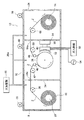
図1に、本発明の機能性フィルムの製造方法の一例を実施する、プラズマCVD装置の一例を概念的に示す。
図1に示すプラズマCVD装置10(以下、CVD装置10とする)は、長尺な基板Z(ウエブ状のフィルム原反)を長手方向に搬送しつつ、この基板Zの表面に、CCP−CVD(Capacitively Coupled Plasma(容量結合プラズマ)−CVD)による成膜を行って、ガスバリアフィルムや各種の光学フィルムなどの機能性フィルムを製造するものである。
また、このCVD装置10は、長尺な基板Zをロール状に巻回してなる基板ロール12から基板Zを送り出し、基板Zを長手方向に搬送しつつ成膜を行って、成膜済の基板Zを巻取り軸14に、再度、ロール状に巻き取る、いわゆるロール・ツー・ロール(Roll to Roll 以下、RtoRともいう)による成膜を行なう装置である。
In FIG. 1, an example of the plasma CVD apparatus which implements an example of the manufacturing method of the functional film of this invention is shown notionally.
A plasma CVD apparatus 10 (hereinafter referred to as a CVD apparatus 10) shown in FIG. 1 conveys a long substrate Z (web-shaped film original fabric) in the longitudinal direction, and on the surface of the substrate Z, CCP-CVD. Film formation by (Capacitively Coupled Plasma (Capacitively Coupled Plasma) -CVD) is performed to manufacture functional films such as gas barrier films and various optical films.
Further, the
本発明の製造方法において、成膜を行う基板(基材/基体)Zには、特に限定はなく、プラズマCVDによる成膜が可能な、各種の長尺なシート状物が、全て利用可能である。
具体的には、ポリエチレンテレフタレート(PET)、ポリエチレンナフタレート(PEN)、ポリエチレン、ポリプロピレン、ポリスチレン、ポリアミド、ポリ塩化ビニル、ポリカーボネート、ポリアクリロニトリル、ポリイミド、ポリアクリレート、ポリメタクリレートなどの有機物からなるプラスチック(樹脂)フィルムが、基板Zとして、好適に利用可能である。
In the production method of the present invention, the substrate (base material / substrate) Z on which the film is formed is not particularly limited, and various long sheets that can be formed by plasma CVD can be used. is there.
Specifically, plastics (resins) made of organic substances such as polyethylene terephthalate (PET), polyethylene naphthalate (PEN), polyethylene, polypropylene, polystyrene, polyamide, polyvinyl chloride, polycarbonate, polyacrylonitrile, polyimide, polyacrylate, polymethacrylate, etc. ) A film can be suitably used as the substrate Z.
また、本発明においては、このようなプラスチックフィルム等を支持体として、その上に、保護層、接着層、光反射層、遮光層、平坦化層、緩衝層、応力緩和層等の、各種の機能を得るための層(膜)が形成されているシート状物を基板Zとして用いてもよい。
この際においては、基板の上に1層のみが形成されたシート状物を基板Zとして用いてもよく、あるいは、基板の上に、複数層が形成されたシート状物を基板Zとして用いてもよい。また、基板Zが、基板の上に複数層が形成されたシート状物である場合には同じ層を複数層有してもよい。
Further, in the present invention, such a plastic film or the like is used as a support, and a protective layer, an adhesive layer, a light reflection layer, a light shielding layer, a planarization layer, a buffer layer, a stress relaxation layer, and the like thereon. A sheet-like material on which a layer (film) for obtaining a function is formed may be used as the substrate Z.
In this case, a sheet-like material in which only one layer is formed on the substrate may be used as the substrate Z, or a sheet-like material in which a plurality of layers are formed on the substrate is used as the substrate Z. Also good. Moreover, when the board | substrate Z is a sheet-like object in which the multiple layer was formed on the board | substrate, you may have multiple layers of the same layer.
前述のように、図1に示すCVD装置10は、長尺な基板Zを巻回してなる基板ロール12から基板Zを送り出し、基板Zを長手方向に搬送しつつ成膜を行って、再度、巻取り軸14によってロール状に巻き取る、いわゆるRtoRによる成膜を行なう装置である。このCVD装置10は、供給室18と、成膜室20と、巻取り室24と、大気開放手段26とを有している。
なお、CVD装置10は、図示した部材以外にも、各種のセンサ、搬送ローラ対や基板Zの幅方向の位置を規制するガイド部材など、基板Zを所定の経路で搬送するための各種の部材(搬送手段)等、長尺な基板Zに、RtoRによって、プラズマCVDで成膜を行なう装置が有する各種の部材を有してもよい。
As described above, the
In addition to the illustrated members, the
大気開放手段26は、基板Zへの成膜を停止(成膜を終了)した際に、供給室18、膜室20および巻取り室24を大気開放して、各室を開放可能にするためのものである。図示例において、大気開放手段26は、導入ライン26aによって、供給室18、成膜室20および巻取り室24に接続されている。
大気開放手段26は、フィルタ等によって浄化した大気(装置外部の空気)を導入ライン26aから各室に導入して、供給室18、成膜室20および巻取り室24を大気圧に戻して、大気開放するもので、真空成膜装置(気相成膜(堆積)装置)等で利用されている、公知の大気開放手段である。
The air release means 26 opens the
The air release means 26 introduces air (air outside the apparatus) purified by a filter or the like into each chamber from the
なお、大気開放手段26は、大気を導入することにより、各室を大気開放するのに限定はされず、窒素等の不活性ガスを各室に導入することにより、各室を大気開放するものでもよい。あるいは、大気の導入と不活性ガスの導入とが、選択可能であってもよい。
さらに、大気開放手段26は、供給室18、成膜室20および巻取り室24に均等に大気を導入するものでも、各室毎に大気の導入量を制御可能なものでもよい。
Note that the air release means 26 is not limited to opening each chamber to the atmosphere by introducing the atmosphere, but opening each chamber to the atmosphere by introducing an inert gas such as nitrogen into each chamber. But you can. Alternatively, introduction of air and introduction of inert gas may be selectable.
Further, the air release means 26 may be one that uniformly introduces air into the
供給室18は、回転軸28と、ガイドローラ30と、真空排気手段32とを有する。
長尺な基板Zを巻回した基板ロール12は、供給室18の回転軸28に装填される。
回転軸28に基板ロール12が装填されると、基板Zが基板ロール12から引き出され、供給室18から、成膜室20を通り、巻取り室24の巻取り軸14に至る所定の搬送経路を通紙される(基板Zが、所定の搬送経路を通される)。
CVD装置10においては、基板ロール12からの基板Zの送り出しと、巻取り室24の巻取り軸14における基板Zの巻き取りとを同期して行なって、長尺な基板Zを所定の搬送経路で長手方向に搬送しつつ、成膜室20において、基板Zに、CCP−CVDによる成膜を連続的に行なう。
The
The
When the
In the
供給室18は、図示しない駆動源によって回転軸28を図中時計方向に回転して、基板ロール12から基板Zを送り出し、ガイドローラ30によって所定の経路を案内して、基板Zを、隔壁34に設けられたスリット34aから、成膜室20に送る。
The
図示例のCVD装置10においては、好ましい態様として、供給室18に真空排気手段32を、巻取り室24に真空排気手段70を、それぞれ設けている。CVD装置10においては、成膜中は、それぞれの真空排気手段によって、供給室18および巻取り室24の圧力を、後述する成膜室20の圧力(成膜圧力)に応じた、所定の圧力に保つ。これにより、隣接する室の圧力が、成膜室20の圧力(すなわち、成膜室20での成膜)に影響を与えることを防止している。
真空排気手段32には、特に限定はなく、ターボポンプ、メカニカルブースターポンプ、ドライポンプ、ロータリーポンプなどの真空ポンプ、さらには、クライオコイル等の補助手段、到達真空度や排気量の調整手段等を利用する、真空成膜装置に用いられている公知の(真空)排気手段が、各種、利用可能である。この点に関しては、後述する他の真空排気手段60および70も同様である。
In the
The vacuum evacuation means 32 is not particularly limited, and includes a vacuum pump such as a turbo pump, a mechanical booster pump, a dry pump, and a rotary pump, an auxiliary means such as a cryocoil, a means for adjusting the ultimate vacuum level and the exhaust amount, and the like. Various known (vacuum) evacuation means used in the vacuum film forming apparatus can be used. In this regard, the same applies to the other vacuum exhaust means 60 and 70 described later.
前述のように、基板Zは、ガイドローラ30によって案内されて、隔壁34のスリット34aから成膜室20に搬送される。
成膜室20は、基板Zの表面に、CCP−CVDによって成膜(膜を形成)するものである。図示例において、成膜室20は、ドラム38と、成膜電極40と、ガイドローラ42、46、48および50と、電極カバー52と、高周波電源54と、ガス供給手段56と、電極移動手段58と、真空排気手段60とを有する。また、成膜室20の構成を簡潔かつ明確に示すために、図示は省略するが、成膜室20には、電極カバー52を移動するためのカバー移動手段も、配置されている。
As described above, the substrate Z is guided by the
The
成膜室20のドラム38は、中心線を中心に図中反時計方向に回転する円筒状の部材で、ガイドローラ42および46によって所定の経路に案内された基板Zを、周面の所定領域(所定の巻き掛け角)に掛け回して、基板Zを、後述する成膜電極40に対面する所定位置に保持しつつ、長手方向に搬送する。
The
このドラム38は、CCP−CVDにおける対向電極としても作用する(すなわち、ドラム38と成膜電極40とで電極対を形成する)。
そのため、ドラム38には、バイアス電力を供給するためのバイアス電源を接続してもよく、あるいは、接地してもよい。あるいは、バイアス電源との接続と接地とが、切り換え可能であってもよい。
また、ドラム38は、成膜中の基板Zの温度を調節する温度調整手段を有してもよい。ドラム38の温度調節手段には、特に限定はなく、ドラム内部に冷媒や温媒等を循環する温度調節手段等、各種の温度調節手段が、全て利用可能である。
The
Therefore, the
The
成膜電極40は、基板Zの対向面から成膜ガスを噴射する、CCP−CVDによる成膜に利用される、公知のいわゆるシャワー電極(シャワープレート)である。
図示例において、成膜電極40は、一例として、一面がドラム38(すなわち基板Z)に対面して配置される、内部に空間(ガス供給空間)が形成された、略直方体形状を有する。成膜電極40のドラム38と対向(対面)する面は、ドラム38と周面と平行になるように(すなわち、ドラム38と成膜電極との間隔が全面的に均一になるように)、凹状の曲面となっている。
なお、成膜電極40も、ドラム38と同様、公知の温度調節手段を有してもよい。
The
In the illustrated example, the film-forming
The
この成膜電極40のドラム38と対向する面(すなわち、成膜される基板Zと対向する面(=成膜ガスおよびプラズマに曝される面))が、本発明の製造方法における、成膜電極40の表面である。
また、成膜電極40の表面は、好ましい態様として、所定サイズの微細な凹凸が形成されている(粗面化処理されている)。これにより、成膜中に、この面に堆積した膜が剥離するのを、好適に防止できる。
The surface of the
Moreover, the surface of the film-forming
前述のように、成膜電極40は、いわゆるシャワー電極であり、その表面には、多数のガス供給孔が形成されている。このガス供給孔は、前述の成膜電極40の内部空間(ガス供給空間)に連通している。また、後述するガス供給手段56は、この成膜電極40の内部空間に成膜ガスを供給する。
従って、ガス供給手段56から供給された成膜ガスは、成膜電極40のガス供給孔から、ドラム38(基板Z)と成膜電極40との間に供給される。
As described above, the
Therefore, the film forming gas supplied from the gas supply means 56 is supplied between the drum 38 (substrate Z) and the
なお、本発明において、成膜電極40は、図示例のような曲面を有するものに限定はされず、内部ガス供給空間を有する直方体状であってもよく、あるいは、ドラム周面は平行ではない曲面を有するものであってもよい。
すなわち、本発明においては、CCP−CVDにおいて使用されている公知のシャワー電極が、全て、利用可能である。
In the present invention, the film-forming
That is, in the present invention, all known shower electrodes used in CCP-CVD can be used.
図示例においては、成膜室20には成膜電極40(CCP−CVDによる成膜手段)が、1個、配置されているが、本発明は、これに限定はされず、基板Zの搬送方向に、複数の成膜電極を配列してもよい。この際には、後述する電極カバー52、および、カバー移動手段は、個々の成膜電極に対応して設けられる。
また、本発明は、シャワー電極を用いる構成にも限定はされず、成膜ガスの吹き出し口(成膜ガスの供給手段)を有さない電極と、電極対の間に成膜ガスを供給するノズル等を用いるCCP−CVDであってもよい。
In the illustrated example, one film forming electrode 40 (film forming means by CCP-CVD) is disposed in the
Further, the present invention is not limited to the configuration using shower electrodes, and the film forming gas is supplied between an electrode that does not have a film forming gas blowing port (film forming gas supply means) and the electrode pair. CCP-CVD using a nozzle or the like may be used.
ガス供給手段56は、プラズマCVD装置等の真空成膜装置に用いられる、公知のガス供給手段である。
前述のように、ガス供給手段56は、成膜電極40の内部空間に成膜ガスを供給する。また、成膜電極40の表面(ドラム38との対向面)には、内部空間に連通する多数のガス供給孔が形成されている。従って、成膜電極40に供給された成膜ガスは、このガス供給孔から、成膜電極40とドラム38との間に供給される。
なお、ガス供給手段56から成膜電極40に成膜ガスを供給する供給管は、後述する成膜電極40の移動に応じて、少なくとも一部が、可撓性を有する配管(フレキシブルな配管)となっている。
The gas supply means 56 is a known gas supply means used in a vacuum film forming apparatus such as a plasma CVD apparatus.
As described above, the gas supply means 56 supplies the film forming gas to the internal space of the
The supply pipe for supplying the film forming gas from the
本発明の製造方法で成膜する膜(すなわち、製造する機能性フィルム)には、特に限定はなく、ガスバリア膜(水蒸気バリア膜)、光反射防止膜や波長帯域フィルタ膜などの各種の光学的な特性を発現する膜、保護膜等、製造する機能性フィルムに要求される機能を発現する膜が、各種、成膜可能である。
従って、ガス供給手段56が供給する成膜ガス(プロセスガス/原料ガス)は、基板Zの表面に成膜する膜に応じた、公知のものでよい。
例えば、CVD装置10が、基板Zの表面に窒化ケイ素膜を成膜して、ガスバリアフィルムを製造する場合には、ガス供給手段56は、CCP−CVDによる窒化ケイ素膜の成膜に利用される公知の成膜ガスを、成膜電極40に供給すればよい。具体的には、窒化ケイ素膜を成膜する場合には、ガス供給手段56は、成膜ガスとして、シランガス、アンモニアガスおよび水素ガスの組み合わせや、シランガス、アンモニアガスおよび窒素ガスの組み合わせ等を供給すればよい。
The film (that is, the functional film to be manufactured) formed by the manufacturing method of the present invention is not particularly limited, and various optical films such as a gas barrier film (water vapor barrier film), an antireflection film, and a wavelength band filter film are used. Various films that exhibit functions required for a functional film to be manufactured, such as a film exhibiting various characteristics and a protective film, can be formed.
Therefore, the deposition gas (process gas / source gas) supplied by the gas supply means 56 may be a known one corresponding to the film to be deposited on the surface of the substrate Z.
For example, when the
高周波電源54は、成膜電極40に、プラズマ励起電力を供給する電源である。高周波電源54も、13.56MHzの高周波電力を供給する電源等、各種のプラズマCVD装置で利用されている、公知の高周波電源が、全て利用可能である。
なお、高周波電源54から成膜電極40への電力供給線は、少なくとも一部が、可撓性を有する線によって行なう。
The high
Note that at least a part of the power supply line from the high-
真空排気手段60は、プラズマCVDによる成膜のために、成膜室内を排気して、所定の成膜圧力に保つものであり、前述のように、真空成膜装置に利用されている、公知の真空排気手段である。 The vacuum evacuation means 60 is for evacuating the film formation chamber to maintain a predetermined film formation pressure for film formation by plasma CVD, and is known as a vacuum film formation apparatus as described above. The vacuum exhaust means.
なお、本発明の製造方法において、基板Zの搬送速度、成膜圧力、成膜ガスの供給量、プラズマ励起電力の強さなどの成膜条件には、特に限定はない。
すなわち、成膜条件は、通常のプラズマCVDによる成膜と同様、成膜する膜、要求される成膜速度、成膜する膜厚、基板Zの種類等に応じて、適宜、設定すればよい。
In the manufacturing method of the present invention, there are no particular limitations on the film forming conditions such as the transport speed of the substrate Z, the film forming pressure, the amount of film forming gas supplied, and the intensity of plasma excitation power.
That is, film formation conditions may be appropriately set according to the film to be formed, the required film formation speed, the film thickness to be formed, the type of the substrate Z, and the like, as in the case of film formation by normal plasma CVD. .
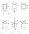
ここで、図示例のCVD装置10においては、成膜室20は、さらに、電極カバー52と、電極移動手段58と、カバー移動手段(図示省略)とを有する。
電極カバー52は、一面が成膜電極40の表面と同じ曲率を有する凸状の曲面を有し、かつ、この曲面が成膜電極40の表面よりもよりも大きな面積を有する、板状の部材(板状のマスク部材)である。従って、電極カバー52の凸状曲面は、成膜電極40の表面の全面に当接して、覆うことができる。
Here, in the
The
電極カバー52は、この凸状曲面を成膜電極40の表面に向けて配置される。さらに、電極カバー52は、カバー移動手段によって水平方向(図1中、紙面と垂直方向)に移動されて、成膜電極40とドラム38との間と、成膜電極40とドラム38との間から退避した位置(成膜に影響を与えない位置)とに、移動される。
また、電極移動手段58は、成膜電極40を、ドラム38に接近する方向、および、ドラム38から離れる方向に移動する。
なお、電極移動手段58およびカバー移動手段は、真空中で動作可能な物であれば、公知の筐体状物や板状物等の移動手段が、各種、移動可能である。
The
Further, the electrode moving means 58 moves the
In addition, as long as the electrode moving means 58 and the cover moving means can operate | move in a vacuum, various moving means, such as a well-known housing-like thing and a plate-like thing, can move.
CVD装置10においては、成膜を停止して、装置内を大気開放する際に、電極カバー52をドラム38と成膜電極40との間に挿入し、次いで、成膜電極40をドラム28に向かって移動して、電極カバー52によって成膜電極40の表面全面を覆った後に、大気開放手段26によって、成膜室20等に大気を導入する(図3参照)。
本発明は、これにより、成膜を停止して大気開放する際に、CVD装置10内に、成膜電極40の表面に付着/堆積した膜が剥離して、パーティクルとなって、装置内部に舞って、飛散することを防止している。
この点に関しては、後に詳述する。
In the
Thus, according to the present invention, when the film formation is stopped and the atmosphere is opened to the atmosphere, the film adhered / deposited on the surface of the
This will be described in detail later.
また、電極カバーは、図示例のような板状の物に限定はされない。例えば、図2に示す電極カバー52aのように、成膜電極40を被嵌して表面全面に接触して覆う、キャップ状(蓋状)の物であってもよい。すなわち、本発明において、電極カバーは、成膜電極40の表面を全面的に覆うものができれば、各種の構成や形状の物が利用可能である。
さらに、電極カバーは、図示例のように、成膜電極40の表面全面に接触して、成膜電極40の表面を覆う構成に限定はされない。例えば、成膜電極40の表面とは離間した状態で表面全面を覆うキャップ状であってもよい。しかしながら、成膜電極40の表面からの膜の剥離/パーティクルの飛散を、より確実に防止できる等の点で、電極カバーは、図1や図2に示される構成のように、成膜電極の表面全面に接触(当接)して、表面全面を覆う構成/形状であるのが好ましい。
Further, the electrode cover is not limited to a plate-like object as shown in the illustrated example. For example, like the
Furthermore, the electrode cover is not limited to a configuration that covers the surface of the film-forming
前述のように、ガイドローラ42および46によって所定の経路に案内された基板Zは、ドラム38の周面に掛け回されて、所定の位置に保持されつつ長手方向に搬送される。ドラム38と成膜電極40とからなる電極対の間では、成膜電極40へのプラズマ励起電力の供給によってプラズマが励起され、成膜ガスからラジカルが生成されて、ドラム38によって支持されつつ搬送される基板Zの表面に、CCP−CVDによって成膜される。
表面に所定の膜を成膜された基板Zは、次いで、ガイドローラ42に案内されて、隔壁64のスリット64aから、巻取り室24に搬送される。
As described above, the substrate Z guided along the predetermined path by the
The substrate Z having a predetermined film formed on the surface is then guided by the
図示例において、巻取り室24は、ガイドローラ68と、巻取り軸14と、真空排気手段70とを有する。
巻取り室24に搬送された基板Zは、ガイドローラ68に案内されて巻取り軸14に搬送され、巻取り軸14によってロール状に巻回されガスバリアフィルムなどの機能性フィルムを巻回してなるロールとして、次の工程に供される。
また、先の供給室18と同様、巻取り室24にも真空排気手段70が配置され、成膜中は、巻取り室24も、成膜室20における成膜圧力に応じた真空度に減圧される。
In the illustrated example, the winding
The substrate Z transported to the winding
Similarly to the
以下、図1および図3を参照して、CVD装置10の作用を説明することにより、本発明の機能性フィルムの製造方法について、より詳細に説明する。
なお、図3の右側の図は、ドラム38、成膜電極40、および、電極カバー52を、図1の右側(巻取り室24側)から見た概念図である。
Hereinafter, the function of the
3 is a conceptual diagram of the
回転軸28に基板ロール12が装填されると、基板Zは、基板ロール12から引き出される。基板ロール12から引き出された基板は、ガイドローラ30によって案内されて成膜室20に至り、成膜室20において、ガイドローラ42および46に案内されて、ドラム38の周面の所定領域に掛け回され、次いで、ガイドローラ48および50によって案内されて巻取り室24に至り、巻取り室24において、ガイドローラ68に案内されて巻取り軸14に至る、所定の搬送経路を通紙される。
When the
基板Zの通紙が終了すると、供給室18、成膜室20および巻取り室24が閉塞される(密閉される)。次いで、真空排気手段32、60、および70が駆動され、供給室18、成膜室20および巻取り室24が、所定の圧力まで減圧される。各室の圧力が安定したら、成膜室20では、ガス供給手段56から成膜電極40に、成膜ガスが供給される。
成膜室20内が成膜に対応する所定圧力で安定したら、供給室18から巻取り室24に向かう基板Zの搬送が、開始され、また、高周波電源54から成膜電極40へのプラズマ励起電力の供給を開始する。
なお、この状態では、電極カバー52は、図3(A)に示すように、ドラム38と成膜電極40との間ではなく、ドラム38と成膜電極40との間の成膜領域から離間した位置(成膜に影響を与えない位置)に配置されている。
When the passing of the substrate Z is completed, the
When the inside of the
In this state, as shown in FIG. 3A, the
供給室18から成膜室20に搬送された基板Zは、ガイドローラ42および46によって案内され、ドラム38に巻き掛けられた状態で搬送されつつ、ドラム38と成膜電極40とが対面している領域において、CCP−CVDによって、窒化ケイ素膜等の目的とする機能を発現する膜を成膜される。
The substrate Z transported from the
所定の膜を成膜された基板Zは、ガイドローラ48および50によって案内されて、巻取り室24に搬送される。
巻取り室24に搬送された基板Zは、ガイドローラ68によって所定の経路に案内され、巻取り軸14によってロール状に巻回される。
The substrate Z on which a predetermined film is formed is guided by the
The substrate Z conveyed to the winding
基板ロール12に巻回される基板Zの量(基板Zの残量)が所定長以下になった場合や、前回の成膜電極40の交換からの合計の成膜時間が所定時間になった場合など、所定の成膜を行なった時点で、高周波電源54から成膜電極40へのプラズマ励起電力の供給、および、ガス供給手段56から成膜電極40への成膜ガスの供給を停止し、さらに、基板Zの搬送を停止して、成膜を停止(終了)する。
次いで、新たな基板ロール12の装填や、成膜電極40の交換等を行なうために、成膜室20、供給室18および巻取り室24の大気開放を行なう。
When the amount of the substrate Z wound around the substrate roll 12 (remaining amount of the substrate Z) becomes a predetermined length or less, or the total film formation time from the previous replacement of the
Next, the
なお、本発明の製造方法において、大気開放は、全部の基板Zを巻取り軸14に巻き取った状態で行なってもよい。すなわち、大気開放を、供給室18および成膜室20に、基板Zが無い状態(基板Zを切った状態)で行なってもよい。
しかしながら、図1等は概念図であるため、ガイドローラは6本しか図示していないが、通常のRtoRによるCVD装置は、多数のガイドローラを有しており、基板Zの通紙には、非常に手間がかかる。また、基板Zが無い状態では、巻取り軸14に巻き取った成膜済の基板Zには、張力が掛かっていない状態となってしまため、この状態で大気開放を行なうと、巻き取った基板Z間に大気が進入してしまい、基板Zの巻回状態が不適性になってしまう。
そのため、本発明の製造方法においては、基板Zを所定の経路で通紙した状態(すなわち、基板ロール12から巻取り軸14まで、所定の張力が掛かった状態)で、以下に示す大気開放を行い、大気開放後、新規な基板ロール12の装填等を行なうのが好ましい。
In the manufacturing method of the present invention, the air release may be performed in a state where all the substrates Z are wound on the winding
However, since FIG. 1 and the like are conceptual diagrams, only six guide rollers are illustrated, but a normal RtoR CVD apparatus has a large number of guide rollers. It takes a lot of work. Further, in the state without the substrate Z, the film-formed substrate Z wound around the winding
Therefore, in the manufacturing method of the present invention, the following air release is performed in a state where the substrate Z is passed through a predetermined path (that is, a state where a predetermined tension is applied from the
CVD装置10において、前述のようにして成膜を停止したら、まず、図3(A)〜図3(B)に示すように、ドラム38と成膜電極40との間の外部に位置していた電極カバー52を、カバー移動手段(図示省略)によって矢印a方向に移動して、ドラム38と成膜電極40との間に位置させる。
次いで、図3(B)〜図3(C)に示すように、電極移動手段58によって、成膜電極40の表面が電極カバー52に接触し、かつ、若干、押圧するまで、成膜電極40をドラム28に接近する方向(矢印b方向)に移動する。
これにより、図3(C)に示すように、成膜電極40の表面全面に電極カバー52を当接して、電極カバー52によって成膜電極40の表面全面を覆う。
When the film formation is stopped in the
Next, as shown in FIG. 3B to FIG. 3C, the
As a result, as shown in FIG. 3C, the
CVD装置10においては、このように、電極カバー52によって成膜電極40の表面全面を覆った状態とした後に、大気開放手段26によって、成膜室20、供給室18および巻取り室24に、大気(外部の空気)を導入する。
すなわち、本発明の製造方法においては、成膜系内(成膜空間内)、言い換えれば、基板Zへの成膜のために減圧される空間内に、成膜電極40の表面(基板Z(対向電極(ドラム38))との対向面)が露出していない状態として、成膜室20、供給室18および巻取り室24に、大気開放を行なうための大気を導入する。
In the
That is, in the manufacturing method of the present invention, the surface of the film-forming electrode 40 (substrate Z (in the film-forming space), in other words, in the space where the pressure is reduced for film-forming on the substrate Z. Assuming that the surface facing the counter electrode (drum 38)) is not exposed, the atmosphere for releasing the atmosphere is introduced into the
前述のように、RtoRを利用してプラズマCVDによって成膜を行なうと、基板Z以外の成膜系内にも、膜が付着/堆積してしまう。特に、プラズマの生成領域すなわち成膜領域(成膜位置)に露出されている成膜電極40の表面には、大量の膜が付着し、堆積してしまう。
このような状態で、装置内を大気開放するために大気を導入すると、成膜電極40の表面に付着/堆積した膜が剥離して、パーティクルとなって成膜系内を舞って、飛翔し、成膜系内全域の至る所に付着してしまう。そのため、パーティクルを除去するための成膜系内のクリーニングに、非常に多くの時間が必要になり、生産性を大幅に低下してしまう。
また、前述のように、大気開放は、基板Zを通紙した状態で行なうのが好ましいが、基板Zを通紙して大気を導入すると、成膜済の基板Z(すなわち製品)にパーティクルが付着して、成膜した膜の損傷や基板Zの汚染等が生じる。さらに、パーティクルが付着した状態で成膜済の基板Zを巻き取ると、成膜済基板Zのロールにパーティクルを巻き込んでしまい、その結果、隣接する基板(積層された基板)にパーティクルが当接し、また、付着して、成膜した膜の損傷や、汚染など、製品としての品質を低下させてしまう。
As described above, when a film is formed by plasma CVD using RtoR, the film is also deposited / deposited in the film forming system other than the substrate Z. In particular, a large amount of film adheres and accumulates on the surface of the
In this state, when the atmosphere is introduced to release the inside of the apparatus, the film adhered / deposited on the surface of the
Further, as described above, it is preferable that the atmosphere is released while the substrate Z is passed through. However, when the substrate Z is passed through and the atmosphere is introduced, particles are formed on the film-formed substrate Z (that is, the product). As a result, the deposited film is damaged or the substrate Z is contaminated. Further, when the film-formed substrate Z is wound with the particles attached, the particles are caught in the roll of the film-formed substrate Z, and as a result, the particles come into contact with the adjacent substrate (laminated substrate). Moreover, the quality of the product as a result of adhesion or damage to the deposited film, contamination, and the like is deteriorated.
これに対し、本発明の製造方法では、電極カバー52によって成膜電極40の表面を覆うなど、成膜系内に成膜電極40の表面が露出していない状態とした後に、成膜系の大気開放のための大気導入を行なう。
そのため、本発明によれば、大気開放のための大気導入を行なっても、成膜基板40の表面に付着/堆積した膜が剥がれるのを、大幅に抑制でき、すなわち、大気の導入によって成膜系内にパーティクルが舞って飛翔するのを、大幅に抑制できる。
その結果、成膜を停止した後、スローベント等を行なわずに迅速に成膜系を大気開放することができ、しかも、大気解放した後の成膜系内のクリーニングに掛かる手間および時間を大幅に低減でき、良好な生産性で機能性フィルムを製造することができる。また、好ましい態様として、基板Zを通紙した状態で大気を導入する場合にも、パーティクルが、成膜済の基板に付着することを防止できるので、パーティクルによる成膜済の基板Zの汚染や膜の損傷、巻回された成膜済基板Zの汚染や損傷等も、好適に防止できる。
加えて、成膜系内のクリーニング性も向上できるので、成膜系内に取りきれないパーティクルが堆積するのも抑制でき、その結果、堆積していく成膜系内の汚れに起因する製品品質の低下も防止して、高品質な製品を長期に渡って安定して製造できる。
On the other hand, in the manufacturing method of the present invention, after the surface of the
Therefore, according to the present invention, even when air introduction for releasing the atmosphere is performed, it is possible to greatly suppress peeling of the film attached / deposited on the surface of the
As a result, after the film formation is stopped, the film formation system can be quickly opened to the atmosphere without performing slow venting, etc., and the labor and time required for cleaning the film formation system after being released to the atmosphere are greatly increased. The functional film can be manufactured with good productivity. Further, as a preferred embodiment, even when the atmosphere is introduced with the substrate Z passed through, particles can be prevented from adhering to the film-formed substrate. Damage to the film, contamination and damage of the wound film-formed substrate Z can be suitably prevented.
In addition, the cleaning performance in the film formation system can be improved, so that it is possible to suppress the accumulation of particles that cannot be removed in the film formation system, and as a result, the product quality due to the dirt in the film formation system that accumulates. It is also possible to stably manufacture high quality products over a long period of time.
このように、電極カバー52によって成膜電極40の表面を覆った後、大気開放手段26によって、成膜室20、供給室18および巻取り室24に大気を導入する。
この大気の導入によって、全ての室が大気圧になったら、電極カバー52および成膜電極40を、成膜中と同じ位置に戻す。なお、大気開放終了後における、電極カバー52と成膜電極40とを成膜中と同じ位置に戻す移動のタイミングは、これに限定はされず、作業の都合等に応じて、適宜、設定すればよい。また、任意のタイミングを選択して、電極カバー52と成膜電極40とを成膜中と同じ位置に戻せるようにしてもよい。
As described above, after the surface of the
When all the chambers become atmospheric pressure due to the introduction of the atmosphere, the
次いで、成膜室20、供給室18および巻取り室24の必要な室を開放する。
その後、新規な基板ロール12の装填(切断した、通紙されている基板Zの後端と、新規ロールの基板Z先端との接続)、巻回した成膜済基板Zの取り外し(切断した基板Zの先端の巻取り軸14への巻回)、成膜電極40の取り外し、成膜室20内の清掃、新規(クリーニング済)の成膜電極40の取付け等の、必要な作業を行なう。
Next, the necessary chambers of the
Thereafter, loading of a new substrate roll 12 (connection between the rear end of the cut-through substrate Z and the front end of the substrate Z of the new roll) and removal of the wound film-formed substrate Z (cut substrate) Necessary operations such as winding the tip of Z around the winding
必要な作業を終了したら、成膜室20、供給室18および巻取り室24を閉塞して、再度、真空排気手段32、60、および70を駆動し、各室が所定の圧力で安定したら、先と同様に、成膜ガスの供給、基板Zの搬送、プラズマ励起電力の供給等を開始して、基板Zへの成膜を再開する。
When the necessary work is completed, the
図示例のCVD装置10においては、電極カバー52の移動手段と、成膜電極40の移動手段とを設けて、直線状(1次元的な)の部材の移動のみで、電極カバー52によって成膜電極40の表面を覆っている。
しかしながら、本発明は、これに限定はされない。すなわち、ドラム38と成膜電極40との間に電極カバー52を挿入した後、電極カバー52を成膜電極40に向けて移動することにより、電極カバー52によって成膜電極40の表面を覆う、2次元的な移動によって、電極カバー52によって成膜電極40の表面を覆ってもよい。
In the
However, the present invention is not limited to this. That is, after the
また、図1および図3に示すCVD装置10は、電極カバー52によって成膜電極40の表面を覆うことで、大気開放のための大気導入時に、成膜系内に成膜電極40の表面が露出していない状態としている。
しかしながら、本発明の製造方法は、これに限定はされず、大気開放のための大気導入時に、成膜系内に成膜電極40の表面が露出していない状態にする方法は、各種の方法が利用可能である。
なお、以下の図4および図5に示す例においては、図1〜図3と同じ部材には同じ符号を付し、説明は、異なる部位を主に行なう。
Further, the
However, the manufacturing method of the present invention is not limited to this, and there are various methods for bringing the surface of the film-forming
In the examples shown in FIGS. 4 and 5 below, the same members as those in FIGS. 1 to 3 are denoted by the same reference numerals, and the description will be mainly made on different parts.
一例として、図4に概念的に示す成膜電極80のように、成膜電極80の表面を、ドラム38と同じ曲率の凹面(あるいは、基板Zの厚さを考慮した同曲率の凹面)として、ドラム38の周面(通紙された基板Z)を、成膜電極80の表面の全面に当接して、成膜電極80の表面を覆う方法が例示される。
すなわち、成膜電極の表面と、対向電極の表面(成膜電極との対向面)とを、互いに全面的に接触可能な形状(凹凸状)として、大気開放のための大気導入時に、成膜電極および/または対向電極を移動して、対向電極によって、成膜電極の表面を全面的に覆うようにしてもよい。
As an example, like the film-forming
In other words, the surface of the film-forming electrode and the surface of the counter electrode (the surface facing the film-forming electrode) are shaped so as to be able to come into full contact with each other (irregularities), and the film is formed when the atmosphere is introduced to open the atmosphere. The electrode and / or the counter electrode may be moved so that the surface of the deposition electrode is entirely covered with the counter electrode.
図4に示す例では、成膜中は、図4(A)に示すように、成膜電極80と、対向電極であるドラム38とは、所定の距離、離間しており、成膜電極80とドラム38との間でプラズマが生成され、基板Zへの成膜が行なわれる。
先の例と同様に、基板Zへの成膜を停止したら、電極移動手段82によって、成膜電極80をドラム38に向かって移動して、ドラム38の周面(基板Z)と、成膜電極80の表面とを、全面的に接触し、好ましくは、成膜電極80によってドラム38を、若干、押圧する。なお、電極移動手段82は、先の電極移動手段58と同様、真空中で駆動可能な公知の移動手段が、各種、利用可能である。
In the example shown in FIG. 4, during film formation, as shown in FIG. 4A, the
Similarly to the previous example, when the film formation on the substrate Z is stopped, the
このように、ドラム38によって成膜電極80の表面全面を覆い、成膜電極80の表面が成膜系に露出していない状態とした後に、先と同様にして、大気開放手段26によって、成膜室20、供給室18および巻取り室24に大気を導入し、各室を大気開放する。
本例でも、先の図1および図3に示される例と同様に、成膜電極80の表面全面がドラム38によって覆われて、成膜系内に露出していないので、大気の導入による成膜電極80表面からの膜の剥離、および、成膜系内へのパーティクルの飛翔を、大幅に抑制することができる。
As described above, after the entire surface of the
In this example as well, as in the example shown in FIGS. 1 and 3, the entire surface of the
ここで、図4に示すように、ドラム38(対向電極)によって成膜電極80の表面を覆う場合にも、基板Zを通紙した状態で、大気開放を行なうのが好ましい。
これにより、前述の各種のメリットに加え、成膜電極80とドラム38とが直接的に当接することが無いので、両者の接触による互いの損傷を防止できる。
Here, as shown in FIG. 4, even when the surface of the film-forming
Thereby, in addition to the various merits described above, the film-forming
また、成膜停止直後は、成膜電極80は、非常に高温になっている。そのため、成膜停止直後に、基板Zに成膜電極80を接触すると、基板Zが熱で損傷する可能性も有る。
一方で、基板ロール12に巻回される基板Zの長さは、当然、既知であり、成膜停止時に、基板Zのどの領域が成膜電極80と対面する位置(成膜領域)に来るのかは、予測ができる。
これを利用して、成膜停止時に、長尺な基板Zにおいて、成膜電極80と対面する位置となる領域(予想される領域)を、ポリイミド等の耐熱性の高い樹脂で形成してもよい。さらに、成膜電極80と基板Z(ドラム38)との密着を、より、好適にするために、成膜停止時に、基板Zの成膜電極80と対面する位置となる領域は、耐熱性に加え、弾性を有する材料で形成してもよい。
Further, immediately after the film formation is stopped, the
On the other hand, the length of the substrate Z wound around the
By utilizing this, even when the film formation is stopped, the region (expected region) that is the position facing the
また、本発明は、何らかの部材によって成膜電極の表面を覆うことにより、大気開放のための大気導入時に、成膜系内に成膜電極40の表面が露出していない状態にするのに限定はされない。
例えば、いわゆるロードロック機構を利用して、大気開放のための大気導入時に、成膜電極を成膜系と気密に分離された別の空間に移動することにより、成膜電極40の表面が成膜系内に露出していない状態としてもよい。
図5に、その一例を概念的に示す。
Further, the present invention is limited to the state in which the surface of the
For example, the surface of the film-forming
FIG. 5 conceptually shows an example thereof.
図5に示す例においては、成膜室20内に、ロードロック室86(成膜電極40の退避室)およびロードロック室90の蓋体90を設け、さらに、ロードロック室86への大気導入手段92、および、成膜電極40の移動手段(図示省略)を設ける。
なお、成膜電極40の移動手段は、前述の電極移動手段58などと同様、真空中で駆動可能な公知の移動手段が、各種、利用可能である。
この装置において、基板Zへの成膜中は、図5(A)に示すように、成膜電極40は、ロードロック室86の外部の、ドラム38とは、所定の距離、離間した位置に配置され、成膜電極80とドラム38との間でプラズマが生成され、基板Zへの成膜が行なわれる。また、蓋体90(図5(A)では省略)は、成膜に影響を与えない位置に退避している。
In the example shown in FIG. 5, a load lock chamber 86 (a retreat chamber for the film formation electrode 40) and a
As the moving means for the
In this apparatus, during film formation on the substrate Z, as shown in FIG. 5A, the
先の例と同様に、基板Zへの成膜を停止したら、図5(B)に示すように、成膜電極40の移動手段によって、成膜電極40をドラム38と離間する方向に移動して、ロードロック室86に収容する。次いで、図示しない移動手段によって、蓋体90を移動して、蓋体90によって、ロードロック室86を気密に閉塞する。これにより、成膜電極40の表面が、成膜系に露出していない状態となる。
なお、蓋体90の移動手段も、前述の例と同様、真空中で駆動可能な公知の移動手段が、各種、利用可能である。
As in the previous example, when the film formation on the substrate Z is stopped, the
As the moving means for the
このように、成膜電極40をロードロック室86に収容して、蓋体90によって、ロードロック室86を気密に閉塞したら、先と同様にして、大気開放手段26によって、成膜室20、供給室18および巻取り室24に大気を導入し、各室を大気開放する。
また、並行して、大気導入手段92によってロードロック室86内に大気(空気)を導入して、ロードロック室86内を大気圧にして、ロードロック室86から成膜電極40を取り出し可能にする。
本例では、成膜電極40は、成膜系内とは気密に離間されたロードロック室86に位置しているので、成膜電極80表面からの剥離した膜は、ロードロック室86内のみで飛翔する。従って、成膜室20等を大気開放するために、各室に大気をしても、成膜系内へのパーティクルの飛翔を、大幅に抑制することができる。
As described above, when the
In parallel, air (air) is introduced into the
In this example, since the
以上、本発明の機能性フィルムの製造方法について詳細に説明したが、本発明は、上記実施例に限定はされず、本発明の要旨を逸脱しない範囲において、各種の改良や変更を行なってもよいのは、もちろんである。
例えば、図1に示す例は、円筒状のドラムの周面に基板Zを巻き掛けた状態で、長手方向に搬送しつつ、成膜を行う装置であるが、本発明は、これに限定はされない。例えば、本発明の製造方法は、直線状(平面状)に基板Zを搬送しつつ、成膜を行う装置にも、好適に利用可能である。すなわち、本発明の製造方法では、長尺な基板を長手方向に搬送しつつ、プラズマCVDによって成膜を行う装置であれば、各種の構成の成膜装置が、全て、利用可能である。
As mentioned above, although the manufacturing method of the functional film of this invention was demonstrated in detail, this invention is not limited to the said Example, Even if various improvement and a change are performed in the range which does not deviate from the summary of this invention. Of course it is good.
For example, the example shown in FIG. 1 is an apparatus for forming a film while transporting it in the longitudinal direction while the substrate Z is wound around the circumferential surface of a cylindrical drum, but the present invention is not limited to this. Not. For example, the manufacturing method of the present invention can also be suitably used for an apparatus that forms a film while conveying the substrate Z in a straight line (planar). That is, in the manufacturing method of the present invention, any film forming apparatus having various configurations can be used as long as the apparatus performs film formation by plasma CVD while transporting a long substrate in the longitudinal direction.
[実施例1]
図1および図3に示すようなCVD装置10を用いて、基板Zの表面に、窒化ケイ素膜を成膜して、ガスバリアフィルムを製造した。
[Example 1]
A gas barrier film was manufactured by forming a silicon nitride film on the surface of the substrate Z using a
ドラム38は、温度調整手段を有する、直径1500mmのステンレス製のドラムを用いた。
基板Zは、厚さ100μmのPETフィルムを用いた。
成膜ガスは、シランガス(SiH4)、アンモニアガス(NH3)、窒素ガス(N2)および水素ガス(H2)を用いた。供給量は、シランガスが100sccm、アンモニアガスが200sccm、窒素ガスが500sccm、水素ガスが500sccmとした。また、成膜圧力は50Paとした。
成膜電極40には、高周波電源54から、周波数13.5MHzで、3000Wのプラズマ励起電力を供給した。さらに、ドラム38には、図示しない電源から、500Wのバイアス電力を供給した。また、成膜中は、ドラム38の温度を−20℃に調整した。
As the
As the substrate Z, a PET film having a thickness of 100 μm was used.
Silane gas (SiH 4 ), ammonia gas (NH 3 ), nitrogen gas (N 2 ), and hydrogen gas (H 2 ) were used as the film forming gas. The supply amounts were 100 sccm for silane gas, 200 sccm for ammonia gas, 500 sccm for nitrogen gas, and 500 sccm for hydrogen gas. The film forming pressure was 50 Pa.
The
上記成膜条件の下、前述のようにして、基板Zに厚さ100nmの窒化ケイ素膜を成膜した。なお、成膜中は、電極カバー52は、ドラム38と成膜電極40との間からは、退避しているのは、前述のとおりである。
成膜を1000m行なった時点で(すなわち1000mのガスバリアフィルムを製造した時点で)、成膜ガス、プラズマ励起電力、およびバイアス電力の供給を停止し、さらに、基板Zの搬送を停止して、成膜を停止した。
次いで、図3(A)〜(C)に示すように、カバー移動手段によって、電極カバー52をドラム38と成膜電極40との間に挿入し、さらに、電極移動手段58によって、成膜電極40をドラム38に向けて移動して、電極カバー52に、若干、押圧し、電極カバー52によって成膜電極40の表面全面を覆った。
Under the above film forming conditions, a silicon nitride film having a thickness of 100 nm was formed on the substrate Z as described above. During the film formation, the
When film formation is performed 1000 m (that is, when a gas barrier film of 1000 m is manufactured), supply of the film formation gas, plasma excitation power, and bias power is stopped, and further, conveyance of the substrate Z is stopped, The membrane was stopped.
Next, as shown in FIGS. 3A to 3C, the
このようにして、電極カバー52によって成膜電極40の表面全面を覆った後に、大気開放手段26によって、成膜室20、供給室18および巻取り室24に、大気(装置外部の空気)を導入して、各室を大気圧に戻した。
なお、大気の導入開始から、全ての室が大気圧になるまでの時間は、40分であった。
Thus, after covering the entire surface of the
Note that the time from the start of the introduction of air to the atmospheric pressure of all the chambers was 40 minutes.
[実施例2]
図5に示す成膜室20を有するCVD装置を用いて、実施例1と、全く同様にして、基板Zに、厚さ100nmの窒化ケイ素膜を成膜して、ガスバリアフィルムを製造した。
なお、このCVD装置は、成膜室20が、電極カバー52、電極移動手段58およびカバー移動手段を有さず、かつ、ロードロック室86、成膜電極40の移動手段、蓋体90、および、蓋体90の移動手段を有する、図5に示す構成である以外は、実施例1で用いたCVD装置10と全く同じ構成を有する。
[Example 2]
A gas barrier film was manufactured by depositing a silicon nitride film having a thickness of 100 nm on the substrate Z in the same manner as in Example 1 by using a CVD apparatus having the
In this CVD apparatus, the
実施例1と同様に、成膜を1000m行なった時点で、成膜ガス、プラズマ励起電力、およびバイアス電力の供給を停止し、さらに基板Zの搬送を停止して、成膜を停止した。
次いで、成膜電極40をロードロック室86に収容し、蓋体90によってロードロック室86を気密に閉塞した。次いで、実施例1と全く同様にして、大気開放手段26によって大気を導入して、各室を大気圧に戻した。また、大気開放手段92によって大気を導入して、ロードロック室86も大気開放した。なお、大気の導入開始から、全ての室が大気圧になるまでの時間は、40分であった。
As in Example 1, when the film formation was performed for 1000 m, the supply of the film formation gas, the plasma excitation power, and the bias power was stopped, the conveyance of the substrate Z was stopped, and the film formation was stopped.
Next, the
[比較例1]
実施例1と全く同様にして、基板Zの表面に厚さ100nmの窒化ケイ素膜を成膜して、ガスバリアフィルムを製造した。
実施例1と同様に、成膜を1000m行なった時点で、成膜ガス、プラズマ励起電力、およびバイアス電力の供給を停止し、さらに基板Zの搬送を停止して、成膜を停止した。
次いで、電極カバー52によって成膜電極40の表面を覆わず、成膜電極40の表面を成膜系内に剥き出しにした状態で、実施例1と全く同様にして、大気開放手段26によって大気を導入して、各室を大気圧に戻した。なお、大気の導入開始から、全ての部屋が大気圧になるまでの時間は、40分であった。
[Comparative Example 1]
In exactly the same manner as in Example 1, a silicon nitride film having a thickness of 100 nm was formed on the surface of the substrate Z to produce a gas barrier film.
As in Example 1, when the film formation was performed for 1000 m, the supply of the film formation gas, the plasma excitation power, and the bias power was stopped, the conveyance of the substrate Z was stopped, and the film formation was stopped.
Next, in a state where the surface of the
[評価]
上記実施例1、実施例2、および、比較例において、大気開放を行なった後、ガイドローラ48からスリット64aまでの間において、成膜済の基板Zをサンプリングして、光学顕微鏡で観察した。その結果、実施例1および実施例2では、成膜した窒化ケイ素膜の剥離やクラックは、認められなかった。これに対し、比較例では、成膜した窒化ケイ素膜の剥離やクラックが確認された。
また。サンプリングした基板Z(ガスバリアフィルム)の水蒸気透過率[g/(m2・day)]を、カルシウム腐食法(特開2005−283561号公報に記載される方法)によって、測定した。その結果、水蒸気透過率は、実施例1が、1.2×10-3[g/(m2・day)]、実施例2が、1.7×10-3[g/(m2・day)]、比較例が、7.4×10-1[g/(m2・day)]であった。
[Evaluation]
In Example 1, Example 2, and Comparative Example, after the atmosphere was released, the film-formed substrate Z was sampled between the
Also. The water vapor permeability [g / (m 2 · day)] of the sampled substrate Z (gas barrier film) was measured by the calcium corrosion method (method described in JP-A-2005-283561). As a result, the water vapor transmission rate was 1.2 × 10 −3 [g / (m 2 · day)] in Example 1, and 1.7 × 10 −3 [g / (m 2 · day) in Example 2. day)], the comparative example was 7.4 × 10 −1 [g / (m 2 · day)].
また、実施例1および比較例では、大気開放を行なった後、装置内のクリーニングを行なって、再度、全く同様にして、1000mの基板Zに酸化ケイ素膜を成膜した。
なお、実施例1では、パーティクルによる装置内の汚染が極めて少なく、装置内のクリーニングは約30分で終了し、迅速に、2回目の成膜を開始できた。これに対し、比較例では、装置内全体にパーティクルが飛散して、壁面等に付着しており、装置内のクリーニングに約90分の時間が掛かってしまった。
In Example 1 and the comparative example, after the atmosphere was released, the inside of the apparatus was cleaned, and a silicon oxide film was formed on the substrate Z of 1000 m in exactly the same manner.
In Example 1, the contamination of the inside of the apparatus by the particles was extremely small, and the cleaning inside the apparatus was completed in about 30 minutes, and the second film formation could be started quickly. On the other hand, in the comparative example, particles scattered throughout the apparatus and adhered to the wall surface or the like, and it took about 90 minutes to clean the apparatus.
2回目の成膜で酸化ケイ素膜を成膜した基板Zについて、ガイドローラ48からスリット64aまでの間のみならず、巻取り軸14に巻き取られた領域からも100m間隔で10点をサンプリングして、先と同様に、水蒸気透過率[g/(m2・day)]を測定した。
その結果、実施例1では、全てのサンプルが、1.2×10⁻³[g/(m2・day)]前後の水蒸気透過率であった。これに対して、比較例の水蒸気透過率は、ガイドローラ48からスリット64aまでの間のサンプルは先と同じく7.4×10-1[g/(m2・day)]であり、巻取り軸14に巻き取られた領域のサンプルは2.5×10-2[g/(m2・day)]前後であった。
With respect to the substrate Z on which the silicon oxide film was formed in the second film formation, 10 points were sampled not only between the
As a result, in Example 1, all samples had a water vapor transmission rate of around 1.2 × 10 −3 [g / (m 2 · day)]. On the other hand, the water vapor transmission rate of the comparative example is 7.4 × 10 -1 [g / (m 2 · day)] for the sample between the
従来のように、成膜電極40の表面を成膜系内に露出した状態で大気開放のための大気導入を行なう比較例は、大気導入によって、成膜電極40の表面に付着/堆積した膜が剥離して、パーティクルとなって装置内を舞って、飛翔し、これが、窒化ケイ素膜を損傷し、ガスバリア性を低下させたと考えられる。
これに対して、成膜電極40の表面を成膜系内に露出しない状態として、大気開放のための大気導入を行なった実施例1および実施例2は、窒化ケイ素膜の損傷およびガスバリア性の低下が認められなかった。この結果より、成膜電極40の表面を成膜系内に露出しないで大気導入を行なった実施例1および実施例2は、成膜電極40の表面に付着/堆積した膜が剥離して、装置内部で舞うことを、大幅に抑制できたと考えられる。
As in the prior art, the comparative example in which the atmosphere is introduced to open the atmosphere with the surface of the film-forming
On the other hand, Example 1 and Example 2 in which the atmosphere was introduced to release the atmosphere with the surface of the
また、2回目の成膜において、実施例1では、成膜した全域において、適正なガスバリア性が得られた。
これに対し、比較例では、装置内に付着したパーティクルが多いため、クリーニングを行なってもパーティクルを完全に取り除くことができなかったと思われる。そのため、ガイドローラ等に残存したパーティクルが、2回目の成膜の際に、基板Zの表裏面や酸化ケイ素に付着してしまい、これが酸化ケイ素膜の損傷等を招き、成膜した全域において、ガスバリア性が低下したと考えられる。すなわち、比較例では、前回の成膜/クリーニングで残存したパーティクルが、次回の成膜に悪影響を及ぼしてしまい、製品全域において適正な性能を得ることができなかった。
以上の結果より、本発明の効果は、明らかである。
In the second film formation, in Example 1, an appropriate gas barrier property was obtained in the entire film formation region.
On the other hand, in the comparative example, since there are many particles adhering in the apparatus, it seems that the particles could not be completely removed even after cleaning. Therefore, particles remaining on the guide roller or the like adhere to the front and back surfaces of the substrate Z and silicon oxide during the second film formation, which causes damage to the silicon oxide film, etc. It is thought that the gas barrier property was lowered. That is, in the comparative example, the particles remaining in the previous film formation / cleaning have an adverse effect on the next film formation, and appropriate performance cannot be obtained in the entire product.
From the above results, the effect of the present invention is clear.
ガスバリアフィルムや反射防止フィルムの製造など、各種の機能性フィルムの製造に、好適に利用可能である。 It can use suitably for manufacture of various functional films, such as manufacture of a gas barrier film and an antireflection film.
10 (プラズマ)CVD装置
12 基板ロール
14 巻取り軸
18 供給室
20 成膜室
24 巻取り室
26 大気開放手段
28 回転軸
30,42,46,48,50,68 ガイドローラ
32,60,70 真空排気手段
34,64 隔壁
38 ドラム
40,80 成膜電極
52 電極カバー
54 高周波電源
56 ガス供給手段
58,82 電極移動手段
DESCRIPTION OF SYMBOLS 10 (Plasma)
Claims (10)
前記基板への成膜を停止して成膜系内を大気解放する際に、前記プラズマCVDによる成膜を行なうための成膜電極の表面を所定のカバーで覆うことにより、前記成膜電極の表面が、前記成膜系内に露出していない状態とした後に、前記大気解放を行なうための気体を成膜系内に導入することを特徴とする機能性フィルムの製造方法。 While carrying a film on the surface of the substrate by plasma CVD while conveying a long substrate in the longitudinal direction,
When the film formation on the substrate is stopped and the inside of the film formation system is opened to the atmosphere , the surface of the film formation electrode for performing the film formation by plasma CVD is covered with a predetermined cover . A method for producing a functional film, comprising introducing a gas for releasing the atmosphere into the film forming system after the surface is not exposed in the film forming system.
前記基板への成膜を停止して成膜系内を大気解放する際に、前記プラズマCVDによる成膜を行なうための成膜電極の表面が、前記成膜系内に露出していない状態とした後に、前記大気解放を行なうための気体を成膜系内に導入するものであり、かつ、When the film formation on the substrate is stopped and the film formation system is released to the atmosphere, the surface of the film formation electrode for performing the film formation by plasma CVD is not exposed in the film formation system; Then, a gas for performing the air release is introduced into the film forming system, and
前記成膜電極の表面と、この成膜電極と電極対を成す対向電極の表面とが、互いに全面的に接触可能な形状を有し、前記成膜電極の表面を対向電極の表面に当接することにより、前記成膜電極の表面が成膜系内に露出していない状態とすることを特徴とする機能性フィルムの製造方法。The surface of the film-forming electrode and the surface of the counter electrode that forms an electrode pair with the film-forming electrode have a shape that can be brought into full contact with each other, and the surface of the film-forming electrode is in contact with the surface of the counter electrode Thereby, the surface of the said film-forming electrode is made into the state which is not exposed in the film-forming system, The manufacturing method of the functional film characterized by the above-mentioned.
前記基板への成膜を停止して成膜系内を大気解放する際に、前記プラズマCVDによる成膜を行なうための成膜電極を、前記成膜系と気密に分離された別の空間に位置させることにより、前記成膜電極の表面が、前記成膜系内に露出していない状態とした後に、前記大気解放を行なうための気体を成膜系内に導入することを特徴とする機能性フィルムの製造方法。When the film formation on the substrate is stopped and the inside of the film formation system is released to the atmosphere, the film formation electrode for performing the film formation by the plasma CVD is placed in a separate space hermetically separated from the film formation system. A function of introducing a gas for releasing the atmosphere into the film forming system after the surface of the film forming electrode is not exposed in the film forming system by being positioned. For producing a conductive film.
Priority Applications (4)
| Application Number | Priority Date | Filing Date | Title |
|---|---|---|---|
| JP2011050108A JP5651502B2 (en) | 2011-03-08 | 2011-03-08 | Method for producing functional film |
| PCT/JP2012/054725 WO2012121040A1 (en) | 2011-03-08 | 2012-02-27 | Method for manufacturing functional film |
| KR1020137021409A KR101622449B1 (en) | 2011-03-08 | 2012-02-27 | Method for manufacturing functional film |
| US14/012,424 US8986795B2 (en) | 2011-03-08 | 2013-08-28 | Manufacturing method of functional film |
Applications Claiming Priority (1)
| Application Number | Priority Date | Filing Date | Title |
|---|---|---|---|
| JP2011050108A JP5651502B2 (en) | 2011-03-08 | 2011-03-08 | Method for producing functional film |
Publications (2)
| Publication Number | Publication Date |
|---|---|
| JP2012184492A JP2012184492A (en) | 2012-09-27 |
| JP5651502B2 true JP5651502B2 (en) | 2015-01-14 |
Family
ID=46798008
Family Applications (1)
| Application Number | Title | Priority Date | Filing Date |
|---|---|---|---|
| JP2011050108A Expired - Fee Related JP5651502B2 (en) | 2011-03-08 | 2011-03-08 | Method for producing functional film |
Country Status (4)
| Country | Link |
|---|---|
| US (1) | US8986795B2 (en) |
| JP (1) | JP5651502B2 (en) |
| KR (1) | KR101622449B1 (en) |
| WO (1) | WO2012121040A1 (en) |
Families Citing this family (3)
| Publication number | Priority date | Publication date | Assignee | Title |
|---|---|---|---|---|
| CN104040023B (en) * | 2012-01-16 | 2016-04-13 | 株式会社爱发科 | Film deposition system |
| JP6801887B2 (en) * | 2018-10-18 | 2020-12-16 | 株式会社クリエイティブコーティングス | Film deposition equipment |
| JP2023528469A (en) * | 2020-06-04 | 2023-07-04 | アプライド マテリアルズ インコーポレイテッド | Vapor deposition apparatus and method for coating a substrate in a vacuum chamber |
Family Cites Families (5)
| Publication number | Priority date | Publication date | Assignee | Title |
|---|---|---|---|---|
| JP3975387B2 (en) * | 2000-02-14 | 2007-09-12 | 富士電機ホールディングス株式会社 | Method of manufacturing shower electrode for thin film forming apparatus by plasma discharge |
| JP2003142472A (en) * | 2001-11-07 | 2003-05-16 | Hitachi Ltd | Method of manufacturing semiconductor device |
| JP4669017B2 (en) * | 2008-02-29 | 2011-04-13 | 富士フイルム株式会社 | Film forming apparatus, gas barrier film, and gas barrier film manufacturing method |
| JP5319373B2 (en) * | 2009-04-10 | 2013-10-16 | 富士フイルム株式会社 | Gas barrier film and method for producing gas barrier film |
| JP5562723B2 (en) * | 2009-05-29 | 2014-07-30 | 富士フイルム株式会社 | Film forming method, film forming apparatus, and gas barrier film manufacturing method |
-
2011
- 2011-03-08 JP JP2011050108A patent/JP5651502B2/en not_active Expired - Fee Related
-
2012
- 2012-02-27 KR KR1020137021409A patent/KR101622449B1/en active IP Right Grant
- 2012-02-27 WO PCT/JP2012/054725 patent/WO2012121040A1/en active Application Filing
-
2013
- 2013-08-28 US US14/012,424 patent/US8986795B2/en not_active Expired - Fee Related
Also Published As
| Publication number | Publication date |
|---|---|
| US20130344257A1 (en) | 2013-12-26 |
| US8986795B2 (en) | 2015-03-24 |
| JP2012184492A (en) | 2012-09-27 |
| KR20140018875A (en) | 2014-02-13 |
| KR101622449B1 (en) | 2016-05-18 |
| WO2012121040A1 (en) | 2012-09-13 |
Similar Documents
| Publication | Publication Date | Title |
|---|---|---|
| JP4669017B2 (en) | Film forming apparatus, gas barrier film, and gas barrier film manufacturing method | |
| JP5665290B2 (en) | Deposition equipment | |
| JP5486249B2 (en) | Deposition method | |
| JP5281606B2 (en) | Method for producing functional film | |
| JP5542488B2 (en) | Deposition equipment | |
| KR101844068B1 (en) | Film deposition device | |
| JP2012052170A (en) | Method of producing functional film | |
| JP2009179427A (en) | Conveying device and vacuum film deposition device | |
| JP5562723B2 (en) | Film forming method, film forming apparatus, and gas barrier film manufacturing method | |
| JP2009280873A (en) | Method of manufacturing gas barrier film | |
| JP2011046060A (en) | Gas barrier film and method for manufacturing gas barrier film | |
| JP2017507247A (en) | Apparatus and method for thin film processing applications | |
| JP5651502B2 (en) | Method for producing functional film | |
| JP5144393B2 (en) | Plasma CVD film forming method and plasma CVD apparatus | |
| JP2010070837A (en) | Film roll and cleaning method for film deposition system | |
| KR102494152B1 (en) | Deposition apparatus of roll-to-roll type | |
| JP5484846B2 (en) | Functional membrane manufacturing apparatus and manufacturing method | |
| JP5450202B2 (en) | Deposition equipment | |
| JP2011179084A (en) | Atmospheric plasma apparatus | |
| JP2010215967A (en) | Method for manufacturing gas barrier film, gas barrier film for solar battery, and gas barrier film for display | |
| JP2009074154A (en) | Film deposition system | |
| JP2011111628A (en) | Film deposition method | |
| JP2012077315A (en) | Functional film and method for manufacturing functional film | |
| JP5713842B2 (en) | Deposition equipment | |
| JP2012229477A (en) | Method for manufacturing functional film |
Legal Events
| Date | Code | Title | Description |
|---|---|---|---|
| A621 | Written request for application examination |
Free format text: JAPANESE INTERMEDIATE CODE: A621 Effective date: 20130617 |
|
| A131 | Notification of reasons for refusal |
Free format text: JAPANESE INTERMEDIATE CODE: A131 Effective date: 20140826 |
|
| A521 | Request for written amendment filed |
Free format text: JAPANESE INTERMEDIATE CODE: A523 Effective date: 20141017 |
|
| TRDD | Decision of grant or rejection written | ||
| A01 | Written decision to grant a patent or to grant a registration (utility model) |
Free format text: JAPANESE INTERMEDIATE CODE: A01 Effective date: 20141111 |
|
| A61 | First payment of annual fees (during grant procedure) |
Free format text: JAPANESE INTERMEDIATE CODE: A61 Effective date: 20141117 |
|
| R150 | Certificate of patent or registration of utility model |
Ref document number: 5651502 Country of ref document: JP Free format text: JAPANESE INTERMEDIATE CODE: R150 |
|
| R250 | Receipt of annual fees |
Free format text: JAPANESE INTERMEDIATE CODE: R250 |
|
| R250 | Receipt of annual fees |
Free format text: JAPANESE INTERMEDIATE CODE: R250 |
|
| R250 | Receipt of annual fees |
Free format text: JAPANESE INTERMEDIATE CODE: R250 |
|
| R250 | Receipt of annual fees |
Free format text: JAPANESE INTERMEDIATE CODE: R250 |
|
| LAPS | Cancellation because of no payment of annual fees |