JP5637693B2 - Photoelectric conversion device and imaging system - Google Patents
Photoelectric conversion device and imaging system Download PDFInfo
- Publication number
- JP5637693B2 JP5637693B2 JP2010012582A JP2010012582A JP5637693B2 JP 5637693 B2 JP5637693 B2 JP 5637693B2 JP 2010012582 A JP2010012582 A JP 2010012582A JP 2010012582 A JP2010012582 A JP 2010012582A JP 5637693 B2 JP5637693 B2 JP 5637693B2
- Authority
- JP
- Japan
- Prior art keywords
- insulating film
- photoelectric conversion
- plane
- light
- region
- Prior art date
- Legal status (The legal status is an assumption and is not a legal conclusion. Google has not performed a legal analysis and makes no representation as to the accuracy of the status listed.)
- Active
Links
- 238000006243 chemical reaction Methods 0.000 title claims description 96
- 238000003384 imaging method Methods 0.000 title claims description 26
- 238000009792 diffusion process Methods 0.000 claims description 71
- 238000000034 method Methods 0.000 claims description 35
- 238000012545 processing Methods 0.000 claims description 25
- 230000002093 peripheral effect Effects 0.000 claims description 22
- 239000000463 material Substances 0.000 claims description 20
- VYPSYNLAJGMNEJ-UHFFFAOYSA-N Silicium dioxide Chemical compound O=[Si]=O VYPSYNLAJGMNEJ-UHFFFAOYSA-N 0.000 claims description 18
- 229910052814 silicon oxide Inorganic materials 0.000 claims description 18
- RYGMFSIKBFXOCR-UHFFFAOYSA-N Copper Chemical compound [Cu] RYGMFSIKBFXOCR-UHFFFAOYSA-N 0.000 claims description 17
- 229910052802 copper Inorganic materials 0.000 claims description 16
- 239000010949 copper Substances 0.000 claims description 16
- 230000008569 process Effects 0.000 claims description 9
- XAGFODPZIPBFFR-UHFFFAOYSA-N aluminium Chemical compound [Al] XAGFODPZIPBFFR-UHFFFAOYSA-N 0.000 claims description 8
- 229910052782 aluminium Inorganic materials 0.000 claims description 8
- IJGRMHOSHXDMSA-UHFFFAOYSA-N Atomic nitrogen Chemical compound N#N IJGRMHOSHXDMSA-UHFFFAOYSA-N 0.000 claims description 6
- 230000003287 optical effect Effects 0.000 claims description 6
- 238000005498 polishing Methods 0.000 claims description 6
- OKTJSMMVPCPJKN-UHFFFAOYSA-N Carbon Chemical compound [C] OKTJSMMVPCPJKN-UHFFFAOYSA-N 0.000 claims description 3
- QVGXLLKOCUKJST-UHFFFAOYSA-N atomic oxygen Chemical compound [O] QVGXLLKOCUKJST-UHFFFAOYSA-N 0.000 claims description 3
- 229910052799 carbon Inorganic materials 0.000 claims description 3
- 229910052757 nitrogen Inorganic materials 0.000 claims description 3
- 229910052760 oxygen Inorganic materials 0.000 claims description 3
- 239000001301 oxygen Substances 0.000 claims description 3
- 239000002210 silicon-based material Substances 0.000 claims description 3
- QUQFTIVBFKLPCL-UHFFFAOYSA-L copper;2-amino-3-[(2-amino-2-carboxylatoethyl)disulfanyl]propanoate Chemical compound [Cu+2].[O-]C(=O)C(N)CSSCC(N)C([O-])=O QUQFTIVBFKLPCL-UHFFFAOYSA-L 0.000 claims 1
- 239000011229 interlayer Substances 0.000 description 69
- 239000010410 layer Substances 0.000 description 63
- 230000001629 suppression Effects 0.000 description 42
- 239000004065 semiconductor Substances 0.000 description 14
- 239000000758 substrate Substances 0.000 description 13
- 229910052581 Si3N4 Inorganic materials 0.000 description 11
- HQVNEWCFYHHQES-UHFFFAOYSA-N silicon nitride Chemical compound N12[Si]34N5[Si]62N3[Si]51N64 HQVNEWCFYHHQES-UHFFFAOYSA-N 0.000 description 11
- 230000002265 prevention Effects 0.000 description 9
- 230000015572 biosynthetic process Effects 0.000 description 5
- 238000005229 chemical vapour deposition Methods 0.000 description 5
- 238000010586 diagram Methods 0.000 description 5
- 238000009826 distribution Methods 0.000 description 5
- 238000001312 dry etching Methods 0.000 description 5
- 238000001459 lithography Methods 0.000 description 5
- 238000004519 manufacturing process Methods 0.000 description 4
- 238000002161 passivation Methods 0.000 description 4
- 238000004088 simulation Methods 0.000 description 4
- 239000004020 conductor Substances 0.000 description 3
- 230000006870 function Effects 0.000 description 3
- OAICVXFJPJFONN-UHFFFAOYSA-N Phosphorus Chemical compound [P] OAICVXFJPJFONN-UHFFFAOYSA-N 0.000 description 2
- 238000004364 calculation method Methods 0.000 description 2
- 230000007423 decrease Effects 0.000 description 2
- 230000000694 effects Effects 0.000 description 2
- 238000005516 engineering process Methods 0.000 description 2
- 238000011156 evaluation Methods 0.000 description 2
- 239000012535 impurity Substances 0.000 description 2
- 238000000059 patterning Methods 0.000 description 2
- 239000011347 resin Substances 0.000 description 2
- 229920005989 resin Polymers 0.000 description 2
- 230000035945 sensitivity Effects 0.000 description 2
- 229910004298 SiO 2 Inorganic materials 0.000 description 1
- 230000009471 action Effects 0.000 description 1
- 238000013459 approach Methods 0.000 description 1
- 230000008901 benefit Effects 0.000 description 1
- 238000012937 correction Methods 0.000 description 1
- 238000011161 development Methods 0.000 description 1
- 230000009977 dual effect Effects 0.000 description 1
- 238000000609 electron-beam lithography Methods 0.000 description 1
- 238000002955 isolation Methods 0.000 description 1
- 230000000737 periodic effect Effects 0.000 description 1
- 238000000206 photolithography Methods 0.000 description 1
- 229910021420 polycrystalline silicon Inorganic materials 0.000 description 1
- 229920005591 polysilicon Polymers 0.000 description 1
- 230000001681 protective effect Effects 0.000 description 1
- 230000005855 radiation Effects 0.000 description 1
- 230000009467 reduction Effects 0.000 description 1
- 238000011160 research Methods 0.000 description 1
- HBMJWWWQQXIZIP-UHFFFAOYSA-N silicon carbide Chemical compound [Si+]#[C-] HBMJWWWQQXIZIP-UHFFFAOYSA-N 0.000 description 1
- 229910010271 silicon carbide Inorganic materials 0.000 description 1
- -1 silicon nitride Chemical compound 0.000 description 1
- 230000003595 spectral effect Effects 0.000 description 1
- 239000000126 substance Substances 0.000 description 1
- 238000002834 transmittance Methods 0.000 description 1
Images


Classifications
-
- H—ELECTRICITY
- H01—ELECTRIC ELEMENTS
- H01L—SEMICONDUCTOR DEVICES NOT COVERED BY CLASS H10
- H01L27/00—Devices consisting of a plurality of semiconductor or other solid-state components formed in or on a common substrate
- H01L27/14—Devices consisting of a plurality of semiconductor or other solid-state components formed in or on a common substrate including semiconductor components sensitive to infrared radiation, light, electromagnetic radiation of shorter wavelength or corpuscular radiation and specially adapted either for the conversion of the energy of such radiation into electrical energy or for the control of electrical energy by such radiation
- H01L27/144—Devices controlled by radiation
- H01L27/146—Imager structures
- H01L27/14601—Structural or functional details thereof
- H01L27/14625—Optical elements or arrangements associated with the device
- H01L27/14629—Reflectors
-
- H—ELECTRICITY
- H01—ELECTRIC ELEMENTS
- H01L—SEMICONDUCTOR DEVICES NOT COVERED BY CLASS H10
- H01L27/00—Devices consisting of a plurality of semiconductor or other solid-state components formed in or on a common substrate
- H01L27/14—Devices consisting of a plurality of semiconductor or other solid-state components formed in or on a common substrate including semiconductor components sensitive to infrared radiation, light, electromagnetic radiation of shorter wavelength or corpuscular radiation and specially adapted either for the conversion of the energy of such radiation into electrical energy or for the control of electrical energy by such radiation
- H01L27/144—Devices controlled by radiation
- H01L27/146—Imager structures
- H01L27/14601—Structural or functional details thereof
- H01L27/14625—Optical elements or arrangements associated with the device
- H01L27/14627—Microlenses
-
- H—ELECTRICITY
- H01—ELECTRIC ELEMENTS
- H01L—SEMICONDUCTOR DEVICES NOT COVERED BY CLASS H10
- H01L31/00—Semiconductor devices sensitive to infrared radiation, light, electromagnetic radiation of shorter wavelength or corpuscular radiation and specially adapted either for the conversion of the energy of such radiation into electrical energy or for the control of electrical energy by such radiation; Processes or apparatus specially adapted for the manufacture or treatment thereof or of parts thereof; Details thereof
- H01L31/02—Details
- H01L31/0232—Optical elements or arrangements associated with the device
- H01L31/02327—Optical elements or arrangements associated with the device the optical elements being integrated or being directly associated to the device, e.g. back reflectors
-
- H—ELECTRICITY
- H01—ELECTRIC ELEMENTS
- H01L—SEMICONDUCTOR DEVICES NOT COVERED BY CLASS H10
- H01L27/00—Devices consisting of a plurality of semiconductor or other solid-state components formed in or on a common substrate
- H01L27/14—Devices consisting of a plurality of semiconductor or other solid-state components formed in or on a common substrate including semiconductor components sensitive to infrared radiation, light, electromagnetic radiation of shorter wavelength or corpuscular radiation and specially adapted either for the conversion of the energy of such radiation into electrical energy or for the control of electrical energy by such radiation
- H01L27/144—Devices controlled by radiation
- H01L27/146—Imager structures
- H01L27/14601—Structural or functional details thereof
- H01L27/14636—Interconnect structures
Landscapes
- Physics & Mathematics (AREA)
- Engineering & Computer Science (AREA)
- Power Engineering (AREA)
- Electromagnetism (AREA)
- Condensed Matter Physics & Semiconductors (AREA)
- General Physics & Mathematics (AREA)
- Computer Hardware Design (AREA)
- Microelectronics & Electronic Packaging (AREA)
- Solid State Image Pick-Up Elements (AREA)
- Transforming Light Signals Into Electric Signals (AREA)
Description
本発明は、光電変換装置、及び撮像システムに関する。 The present invention relates to a photoelectric conversion device and an imaging system.
近年、光電変換装置としてMOSトランジスタを用いたMOS型の光電変換装置が盛んに開発されている。そのような光電変換装置において画素の高密度化や小チップ化が推し進められ、画素における光電変換部(例えば、フォトダイオード)の受光面の面積が小さくなる傾向にある。これに伴って、配線材料はアルミニウムより微細な加工に適した銅への変更が進んでいる。 In recent years, MOS type photoelectric conversion devices using MOS transistors as photoelectric conversion devices have been actively developed. In such a photoelectric conversion device, the density of pixels and the reduction in size of chips are promoted, and the area of the light receiving surface of a photoelectric conversion unit (for example, a photodiode) in the pixel tends to be reduced. In connection with this, the wiring material is changing to copper suitable for finer processing than aluminum.
銅配線を使用する場合には、層間絶縁膜として一般に用いられる酸化膜中での銅原子の拡散係数が大きいために、銅の拡散を防止する拡散防止膜を配する必要がある。銅配線の上層の拡散防止膜としてはシリコン窒化膜を用いる場合が多い。銅に限らず、配線材料の層間絶縁膜中における配線材料の原子の拡散係数が大きい場合には拡散防止膜が必要となる。 When copper wiring is used, since a diffusion coefficient of copper atoms in an oxide film generally used as an interlayer insulating film is large, it is necessary to provide a diffusion preventing film for preventing copper diffusion. In many cases, a silicon nitride film is used as the diffusion prevention film on the upper layer of the copper wiring. When the diffusion coefficient of atoms of the wiring material in the interlayer insulating film of the wiring material is not limited to copper, a diffusion preventing film is necessary.
拡散防止膜を光電変換装置で用いる場合は、層間絶縁膜と拡散防止膜との多層構造が形成される。拡散防止膜に適した膜、たとえばシリコン窒化膜は層間絶縁膜として用いられるシリコン酸化膜と屈折率が異なるため、界面での反射や干渉による影響で光電変換部への入射光量が低下するという課題が発生する。 When the diffusion prevention film is used in a photoelectric conversion device, a multilayer structure of an interlayer insulating film and a diffusion prevention film is formed. A film suitable for a diffusion prevention film, such as a silicon nitride film, has a refractive index different from that of a silicon oxide film used as an interlayer insulating film, so that the amount of light incident on the photoelectric conversion unit is reduced due to reflection and interference at the interface. Will occur.
特許文献1の図1には、各拡散防止膜121、131、141が、フォトダイオード112の受光領域に対応する開口を有することが記載されている。フォトダイオード112の受光領域の上には、SiO2よりなる層間膜115、122、132、142が配されており、層間膜142の上にはSiN保護膜161が配されている。特許文献1には、フォトダイオード112の受光領域上に配置される領域が、単一の屈折率を有するシリコン酸化膜だけで形成されているので、フォトダイオード112への反射や多重干渉の影響を低減できる、と記載されている。
FIG. 1 of Patent Document 1 describes that each diffusion prevention film 121, 131, 141 has an opening corresponding to the light receiving region of the
一方、光リソグラフィ並びに電子線リソグラフィに代表されるプレーナープロセス技術の発展に伴い、基板表面上に可視光の波長以下(サブ波長領域)の寸法を持つ微細パターンの形成が可能となっている。これに伴い、サブ波長領域の周期構造を有する集光素子(SubWaveLength Lens:SWLL)が注目を集めている。「サブ波長領域」とは、対象とする光(可視光)の波長と同程度かそれよりも小さい領域をいう。 On the other hand, with the development of planar process technology represented by optical lithography and electron beam lithography, it is possible to form a fine pattern having a dimension below the wavelength of visible light (subwavelength region) on the substrate surface. Accordingly, a condensing element (SubWaveLength Lens: SWLL) having a periodic structure in the sub-wavelength region is attracting attention. The “sub-wavelength region” refers to a region that is the same as or smaller than the wavelength of the target light (visible light).
非特許文献1には、非球面レンズであるフレネルレンズから変換された格子状のSWLLに集光効果があることが、Delaware大学の研究グループによりシミュレーションで実証されたことが記載されている。 Non-Patent Document 1 describes that a lattice-shaped SWLL converted from a Fresnel lens, which is an aspherical lens, has a light-collecting effect that has been demonstrated by simulation by a research group at the University of Delaware.
上述のように、特許文献1の技術では、各拡散防止膜121、131、141が、フォトダイオード112の受光領域に対応する開口を有する。
As described above, in the technique of Patent Document 1, each diffusion prevention film 121, 131, 141 has an opening corresponding to the light receiving region of the
ここで、仮に、画素の寸法を縮小した場合を考える。この場合、各拡散防止膜121、131、141の開口端における入射光の回折作用により、その開口に入射した光のうち光電変換部の受光面に到達する光の割合が低減する。すなわち、光電変換部へ向けて入射した光のうち光電変換部の受光面へ到達する光の割合が低減するので、光電変換部の感度が低下する。入射光の回折作用は、拡散防止膜の開口端だけに限らず、アルミニウム等の配線の配線開口端においても生じる。 Here, let us consider a case where the pixel size is reduced. In this case, the ratio of the light reaching the light receiving surface of the photoelectric conversion unit out of the light incident on the opening is reduced by the diffraction action of the incident light at the opening end of each diffusion prevention film 121, 131, 141. That is, the ratio of the light that reaches the light receiving surface of the photoelectric conversion unit out of the light incident on the photoelectric conversion unit is reduced, so that the sensitivity of the photoelectric conversion unit is reduced. The diffraction effect of incident light occurs not only at the opening end of the diffusion preventing film but also at the wiring opening end of a wiring such as aluminum.
本発明の目的は、画素の寸法を縮小した場合に、光電変換部へ向けて入射した光のうち光電変換部の受光面へ到達する光の割合を向上させることにある。 An object of the present invention is to improve the proportion of light that reaches the light receiving surface of the photoelectric conversion unit out of the light incident on the photoelectric conversion unit when the size of the pixel is reduced.
本発明の1つの側面は、光電変換装置に係り、該光電変換装置は、受光面を有する光電変換部と、前記光電変換部へ光を集める集光構造と、前記集光構造の下に配され、銅を主成分とする材料で形成された配線層と、を備え、前記集光構造は、第1の絶縁膜と、前記第1の絶縁膜の屈折率より高い屈折率を有し、前記銅を主成分とする材料の拡散を抑制するように前記配線層を覆っている第2の絶縁膜とを含み、前記第2の絶縁膜は、前記受光面に平行な第1の平面に沿って配され、前記第1の絶縁膜は、前記第2の絶縁膜の上面を含む第2の平面と前記第2の絶縁膜の下面を含む第3の平面との間に配され、前記第2の絶縁膜の密度が、前記第1の平面における中心領域において前記第1の平面における周辺領域よりも大きく、前記第1の平面における前記第1の絶縁膜と前記第2の絶縁膜とのレイアウトパターンは、可視光領域の最大波長以下の寸法を有する部分を含む。 One aspect of the present invention relates to a photoelectric conversion device, the photoelectric conversion device includes a photoelectric conversion portion having a light receiving surface, a light collecting structures for collecting light into the photoelectric conversion unit, distribution under the light converging structure It is copper with a wiring layer formed of a material whose main component, the a, the light-collecting structure, possess a first insulating film, a refractive index higher than the refractive index of the first insulating film, A second insulating film covering the wiring layer so as to suppress diffusion of the copper-based material, and the second insulating film is on a first plane parallel to the light receiving surface. And the first insulating film is disposed between a second plane including an upper surface of the second insulating film and a third plane including a lower surface of the second insulating film, A density of the second insulating film is greater in a central region in the first plane than in a peripheral region in the first plane; Layout pattern of the first insulating film in the surface and the second insulating film includes a portion having the following dimensions maximum wavelength in the visible light region.
本発明によれば、光電変換部へ向けて入射した光のうち光電変換部の受光面へ到達する光の割合を向上させることができる。 ADVANTAGE OF THE INVENTION According to this invention, the ratio of the light which reaches | attains the light-receiving surface of a photoelectric conversion part among the light which injected toward the photoelectric conversion part can be improved.
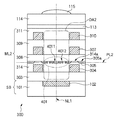
本発明の第1実施形態に係る光電変換装置100を、図1を用いて説明する。図1は、本発明の第1実施形態に係る光電変換装置100の断面構成を示す図である。
A
光電変換装置100は、光電変換部102、配線層(第2の配線層)104、配線層(第1の配線層)107、110、集光構造201、パッシベーション膜113、カラーフィルタ層114、及びマイクロレンズ115を備える。
The
光電変換部102は、受光面102aを有しており、受光面102aに入射した光に応じた電荷を発生させて蓄積する。光電変換部102は、半導体基板SBにおけるウエル領域101に囲まれた半導体領域である。ウエル領域101は、第1の導電型(例えばp型)の不純物を低濃度で含む。光電変換部102は、第1の導電型と反対導電型(例えばn型)の不純物を高濃度で含む。なお、光電変換部102は、半導体基板SBにおける画素配列領域における画素の配列に対応して1次元的に又は2次元的に配列されているが、図1には、説明の簡略化のため、1画素のフォトダイオード部に対応したもののみ示している。
The
配線層104は、集光構造201の下方に配され、光電変換部102に対する開口領域OA1を規定している。配線層104は、例えば、銅を主成分とする材料で形成されており、少なくともその上面が拡散抑制膜(第2の絶縁膜)105により覆われている。配線層107は、集光構造201の上方に配され、光電変換部102に対する開口領域OA1を規定している。配線層107は、例えば、銅を主成分とする材料で形成されており、少なくともその上面が拡散抑制膜108により覆われている。配線層110は、集光構造201の上方に配され、光電変換部102に対する開口領域OA1を規定している。配線層110は、例えば、銅を主成分とする材料で形成されており、少なくともその上面が拡散抑制膜112により覆われている。この実施形態では、開口領域OA1は3つの配線層104、107、110によって規定される。
The
半導体基板SBと配線層104とは、層間絶縁膜(第3の絶縁膜)103により絶縁されている。層間絶縁膜103は、例えば、シリコン酸化物で形成されている。配線層104と配線層107とは、層間絶縁膜(第1の絶縁膜)106により絶縁されている。層間絶縁膜106は、例えば、シリコン酸化物で形成されている。配線層107と配線層110とは、層間絶縁膜109により絶縁されている。層間絶縁膜109は、例えば、シリコン酸化物で形成されている。層間絶縁膜109の上には、層間絶縁膜111が配されている。層間絶縁膜111は、例えば、シリコン酸化物で形成されている。ここで、配線層104、107、110は、それぞれ、層間絶縁膜103、層間絶縁膜106、層間絶縁膜109の上面に形成された溝に銅などの導電体を埋め込み、CMP
工程により、溝内の導電体以外の導電体を除去することにより形成される。配線層104、107、110の構造は、それぞれ、ダマシン構造である。また、配線層104、107、110、拡散抑制層105、108、112、及び層間絶縁膜103、106、109、111は、半導体基板SBの上における多層配線構造を形成している。
The semiconductor substrate SB and the
The step is formed by removing a conductor other than the conductor in the groove. Each of the
集光構造201は、光電変換部102の上方に配され、光電変換部102へ光を集める。集光構造201では、拡散抑制膜105の密度が、中心領域2011において周辺領域2012より大きくなるように、層間絶縁膜106と拡散抑制膜105とが平面PL1にレイアウトされている。中心領域2011は、受光面102aの中心102cを通る法線NL1に垂直な平面PL1における法線NL1の通る領域である。周辺領域2012は、平面PL1における法線NL1からオフセットした領域である。中心領域2011及び周辺領域2012は、開口領域OA1内(開口領域内)に配されている。拡散抑制膜105は、銅を主成分とする材料の拡散を抑制するように、配線層104を覆うとともに平面PL1に沿って延びている。また、拡散抑制膜105は、層間絶縁膜106の屈折率より高い屈折率を有する。拡散抑制膜105は、例えば、シリコン窒化物又はシリコン炭化物など、炭素、酸素、窒素のいずれかを含むシリコン系化合物で形成されている。
The condensing
ここで、平面PL1における層間絶縁膜106と拡散抑制膜105とのレイアウトパターンは、可視光領域の最大波長以下の寸法を有する部分を含む(図2参照)。可視光領域は、一般的には、400nm以上750nm以下の波長の領域である(オプトロニクス社 光技術用語辞典 第3版を参照)。可視光領域の最大波長以下の寸法は、例えば、可視光領域の下限値と上限値との平均値以下の寸法でありうる。あるいは、可視光領域の最大波長以下の寸法は、画素に設けられたカラーフィルタの分光透過率のピークの波長以下の寸法でありうる。あるいは、可視光領域の最大波長以下の寸法は、入射光(例えば放射線)を蛍光体で可視光に変換しその変換された光をマイクロレンズで受ける場合、蛍光体によって変換された光のピーク波長以下の寸法でありうる。
Here, the layout pattern of the
拡散抑制膜105を用いて光電変換部102に対応する開口領域OA1に、入射光の波長以下のパターンの粗密を有する集光構造201を形成する。すなわち、拡散抑制膜105は、開口領域OA1におけるパターニングされた開口を有するとともに平面PL1に沿って延びている。層間絶縁膜106は、拡散抑制膜105における開口を満たしている。集光構造201では、さらに、層間絶縁膜106が拡散抑制膜105の上面を覆うように配され、層間絶縁膜103が拡散抑制膜105の下面を覆うように配されている。層間絶縁膜106及び層間絶縁膜103は、ともに、拡散抑制膜105の屈折率より低い屈折率を有する。そのレイアウトパターンでは、中心領域2011における拡散抑制膜105の密度が、周辺領域2012における拡散抑制膜105の密度より大きい(図2(A)〜(C)参照)。一方、他の拡散抑制膜108及び112は、それぞれ、開口領域OA1に対応した開口108a,112aを有している。
A condensing
パッシベーション膜113は、半導体基板SB及び多層配線構造ML1を保護するように、層間絶縁膜111の上に配されている。カラーフィルタ層114は、パッシベーション膜113の上に配され、マイクロレンズ115を通過した光のうち可視光領域における特定の色(例えば、R,G,B)の波長の光を選択的に透過する。マイクロレンズ115は、カラーフィルタ層114の上に配され、入射した光を屈折させてカラーフィルタ層114へ導く。
The
図1では、集光構造201は、拡散抑制膜105が延びた方向に沿った平面PL1に形成されているが、拡散抑制膜105、108、112の少なくとも1つが延びた方向に沿った平面に形成されていても良い。集光構造201は、1または複数の拡散抑制膜と同じ層に形成されているとも言える。集光構造201は、可視光領域の入射光の波長以下のパターンの粗密を利用し、有効屈折率が光電変換部に対応する開口領域における外周部よりも開口領域における中心部の方が高くなる構造であれば形状は問わない。集光構造における外周部から中心部に向っての有効屈折率の増加率は任意であり、単調増加でもステップ増加でもよい。また、層間絶縁膜103と半導体基板SBとの間に、層間絶縁膜103と半導体基板SBとの界面における入射光の反射を低減させるための反射防止膜が配されていても良い。配線層の数も3層に限られたものではない。層間絶縁膜111とカラーフィルタ層114との間に、さらに層内レンズが設けられていても構わない。
In FIG. 1, the condensing
次に、集光構造201におけるレイアウトパターンの具体例を、図2(A)〜(C)を用いて説明する。図2(A)〜(C)は、それぞれ、集光構造201におけるレイアウトパターンの具体例を示す図である。図2(A)〜(C)では、ハッチングで示した領域が拡散抑制膜105の占める領域であり、ハッチングで示した領域の間における白色で示した領域が層間絶縁膜106の占める領域である。
Next, a specific example of the layout pattern in the
図2(A)に示すレイアウトパターンでは、複数の円が法線NL1を中心として平面PL1(図1参照)に沿って配されている。すなわち、図2(A)に示すレイアウトパターンは、同心円状のパターンである。同心円状のパターンは、粗密分布をもって形成される。同心円の法線NL1近傍の中心領域2011において、層間絶縁膜106の屈折率よりも高い屈折率を有する拡散抑制膜105の密度が高く、同心円の法線NL1からオフセットした周辺領域2012において、高い屈折率を有する拡散抑制膜105の密度が低い。これにより、中心領域2011の有効屈折率が周辺領域2012の有効屈折率より高くなる。
In the layout pattern shown in FIG. 2A, a plurality of circles are arranged along the plane PL1 (see FIG. 1) around the normal line NL1. That is, the layout pattern shown in FIG. 2A is a concentric pattern. The concentric pattern is formed with a dense distribution. In the
例えば、図2(A)に示すレイアウトパターンに対する法線NL1を通るG−G断面における複数の評価点を決定し、その評価点における有効屈折率を計算したところ、図4に示すシミュレーション結果が得られた。図4は、図2(A)に示すレイアウトパターンに対する有効屈折率の分布のシミュレーション結果を示す図である。有効屈折率は、ある入射光の波長に対するある位置の実質的な屈折率を示す数値であり、その位置近傍の屈折率の平均値にほぼ等しい。平面パターンは波長以下の微細なパターンであるため、波長と同等乃至波長より短い周期で屈折率の異なる膜が存在する。例えば、ある点の有効屈折率は、その点を中心とし半径が波長に等しい円内の平均屈折率と考えてよい。図4に示すように有効屈折率は、同心円の中心PNL1が最も高く外周に近づくにつれ小さくなる。これにより、拡散防止膜が完全な開口(図1に示す開口108a,112aのように光が通過する領域に拡散防止膜が存在しない開口。)を有する場合に比べて、図2(A)に示すレイアウトパターンによれば、光電変換部102の受光面102aへ向かうように光を屈折させることが容易になる。例えば、図3に示すように、入射光の波長以下のパターンの粗密を利用し、有効屈折率が外周部よりも中心部の方が高くなる構造にすることによって、光線301が光電変換部102の受光面102aへ向かうように光線301を屈折させることができる。これにより、光電変換部102へ向けて入射した光を受光面102aへ集光させることが容易になる。
For example, when a plurality of evaluation points in the GG cross section passing through the normal line NL1 with respect to the layout pattern shown in FIG. 2A is determined and the effective refractive index at the evaluation points is calculated, the simulation result shown in FIG. 4 is obtained. It was. FIG. 4 is a diagram showing a simulation result of the effective refractive index distribution for the layout pattern shown in FIG. The effective refractive index is a numerical value indicating the substantial refractive index at a certain position with respect to the wavelength of a certain incident light, and is substantially equal to the average value of the refractive indices near the position. Since the planar pattern is a fine pattern having a wavelength equal to or smaller than the wavelength, there are films having different refractive indexes with a period equal to or shorter than the wavelength. For example, the effective refractive index at a certain point may be considered as the average refractive index within a circle centered at that point and having a radius equal to the wavelength. As shown in FIG. 4, the effective refractive index is highest at the center PNL1 of the concentric circle and decreases as it approaches the outer periphery. Thus, as compared with the case where the diffusion prevention film has a complete opening (an opening where the diffusion prevention film does not exist in a region through which light passes, such as the
同様に、図2(B)に例示されるレイアウトパターンでは、複数の多角形(例えば、八角形)が法線NL1を中心として平面PL1(図1参照)に沿って配されている。すなわち、図2(B)に例示されるレイアウトパターンは、同心多角形状のパターンである。同心多角形状のパターンは、粗密分布をもって形成される。同心多角形の法線NL1近傍の中心領域2011において、層間絶縁膜106の屈折率よりも高い屈折率を有する拡散抑制膜105の密度が高く、法線NL1からオフセットした周辺領域2012において、高い屈折率を有する拡散抑制膜105の密度が低い。これにより、中心領域2011の有効屈折率が周辺領域2012の有効屈折率より高くなる。
Similarly, in the layout pattern illustrated in FIG. 2B, a plurality of polygons (for example, octagons) are arranged along the plane PL1 (see FIG. 1) with the normal line NL1 as the center. That is, the layout pattern illustrated in FIG. 2B is a concentric polygonal pattern. The concentric polygonal pattern is formed with a dense distribution. In the
一方、図2(C)に例示されるレイアウトパターンでは、複数のホール又はドットが法線NL1に関して対称に分布するように平面PL1に沿って配されている。すなわち、図2(C)に示すレイアウトパターンは、中心領域2011における拡散抑制膜105のホールの密度が、周辺領域2012における拡散抑制膜105のホールの密度より低くなっている。したがって、法線NL1近傍の中心領域2011において、層間絶縁膜106の屈折率よりも高い屈折率を有する拡散抑制膜105の密度が高く、法線NL1からオフセットした周辺領域2012において、高い屈折率を有する拡散抑制膜105の密度が低い。これにより、中心領域2011の有効屈折率が周辺領域2012の有効屈折率より高くなる。これにより、拡散防止膜が完全な開口(図1に示す開口108a,112aのように光が通過する領域に拡散防止膜が存在しない開口)を有する場合に比べて、光電変換部102の受光面102aへ向かうように光を屈折させることが容易になる。このため、光電変換部102へ向けて入射した光を受光面102aへ集光させることが容易になる。
On the other hand, in the layout pattern illustrated in FIG. 2C, a plurality of holes or dots are arranged along the plane PL1 so as to be distributed symmetrically with respect to the normal line NL1. That is, in the layout pattern shown in FIG. 2C, the hole density in the
このように、第1実施形態では、法線からオフセットした周辺領域に比べて法線近傍の中心領域で有効屈折率が高くなる集光構造を光電変換部の上方に設ける。これにより、光電変換部へ向けて入射した光のうち光電変換部の受光面へ到達する光の割合を向上させることができる。 As described above, in the first embodiment, a light converging structure in which the effective refractive index is higher in the central region near the normal than in the peripheral region offset from the normal is provided above the photoelectric conversion unit. Thereby, the ratio of the light which reaches | attains the light-receiving surface of a photoelectric conversion part among the light which injected toward the photoelectric conversion part can be improved.
次に、本発明の第1実施形態に係る光電変換装置100の製造方法を、図1を用いて説明する。配線材料として銅を用い、層間絶縁膜に配線が埋設されたダマシン構造に関して説明する。
Next, a method for manufacturing the
まず、半導体基板SBに、光電変換部102のほか、トランジスタのソース又はドレインとして機能する複数の半導体領域(不図示)、及び、トランジスタ等の素子間を分離する素子分離領域を形成する(不図示)。そして、半導体基板SB上に、ゲート絶縁膜を形成し、トランジスタのゲート電極(不図示)を例えばポリシリコンで形成し、更に、シリコン酸化膜をCVD法(化学気相成長法)により堆積する。その後、CMP法(化学的機械研磨法)により、そのシリコン酸化膜の平坦化を行う。これにより、層間絶縁膜103を形成する。そして、層間絶縁膜103にコンタクト(不図示)を形成する。
First, in addition to the
次に、ダマシン法により、層間絶縁膜103に配線層104を埋設する。ここで、ダマシン法は、シングルダマシン法、デュアルダマシン法いずれの方法でもよい。その後、シリコン窒化物などにより拡散抑制膜105を全面に形成する。シリコン窒化物105の膜厚は、約30nm以上で設けられ、上限は、配線層104、107間の厚み(400μm)である。その後、リソグラフィ技術及びドライエッチング技術により、光電変換部102に対応した領域に配された拡散抑制膜105を可視光領域の最大波長以下の寸法を有する粗密パターンが同心状に配された集光構造201を形成する。
Next, the
次に、CVD法により層間絶縁膜106としてのシリコン酸化膜を形成する。層間絶縁膜106の形成において、拡散抑制膜105及び集光構造201の段差の影響を低減したい場合には、CMP法を用いてもよい。次に、ダマシン法により、層間絶縁膜106に配線層107を埋設する。この配線層107の形成の前あるいは同時にコンタクト(不図示)が層間絶縁膜106に形成される。その後、シリコン窒化膜などにより拡散抑制膜108を全面に形成した後、リソグラフィ技術及びドライエッチング技術により光電変換部に対応した領域に配された拡散抑制膜108を除去する。しかし、拡散抑制膜108と層間絶縁膜106との屈折率差がそれほど大きくない場合は、そのまま拡散抑制膜108を残してもよい。
Next, a silicon oxide film as an
さらに、CVD法により層間絶縁膜109としてのシリコン酸化膜を形成する。層間絶縁膜109の形成において、拡散抑制膜108の段差の影響を低減したい場合には、CMP法を用いてもよい。次に、ダマシン法により、層間絶縁膜109に配線層110を埋設する。この配線層110の形成の前あるいは同時にコンタクト(不図示)が層間絶縁膜108に形成される。その後、シリコン窒化膜などにより拡散抑制膜112を全面に形成した後、リソグラフィ技術及びドライエッチング技術により光電変換部に対応した領域に配された拡散抑制膜112を除去する。しかし、拡散抑制膜112と層間絶縁膜109との屈折率差がそれほど大きない場合は、拡散抑制膜112をそのまま残してもよい。
Further, a silicon oxide film as the
さらに、CVD法によりシリコン酸化膜を形成し、そのシリコン酸化膜を平坦化することにより、層間絶縁膜111を形成する。層間絶縁膜111の形成において、拡散抑制膜112の段差の影響を低減したい場合には、CMP法を用いてもよい。次に、CVD法によりパッシベ−ション膜113を全面に形成する。その後、樹脂を用いて、平坦化を行う。次に、カラーフィルタ層114をつけ、再度樹脂を用いて平坦化を行う。次に、マイクロレンズ115を形成する。
Further, a silicon oxide film is formed by a CVD method, and the silicon oxide film is planarized to form an
このように、拡散抑制膜105における光電変換部102上に位置した部分をパターンニングする工程を用いて、集光構造201を形成することができる。このような工程により集光構造を多層配線構造中に形成することで、マイクロレンズや公知の層内レンズより受光面102aに近い領域で光を屈折させることができる。このため、より大きな入射角の光や配線層によって回折した光も光電変換部102の受光面102aに到達するようになる。すなわち、簡易な工程でかつ入射光量・感度の低下を低減することができる。
As described above, the condensing
次に、本発明の光電変換装置を適用した撮像システムの一例を図5に示す。 Next, an example of an imaging system to which the photoelectric conversion device of the present invention is applied is shown in FIG.
撮像システム90は、図5に示すように、主として、光学系、撮像装置86及び信号処理部を備える。光学系は、主として、シャッター91、レンズ92及び絞り93を備える。撮像装置86は、光電変換装置100を含む。信号処理部は、主として、撮像信号処理回路95、A/D変換器96、画像信号処理部97、メモリ部87、外部I/F部89、タイミング発生部98、全体制御・演算部99、記録媒体88及び記録媒体制御I/F部94を備える。なお、信号処理部は、記録媒体88を備えなくても良い。
As shown in FIG. 5, the
シャッター91は、光路上においてレンズ92の手前に設けられ、露出を制御する。
The
レンズ92は、入射した光を屈折させて、撮像装置86の光電変換装置100の撮像面に被写体の像を形成する。
The
絞り93は、光路上においてレンズ92と光電変換装置100との間に設けられ、レンズ92を通過後に光電変換装置100へ導かれる光の量を調節する。
The
撮像装置86の光電変換装置100は、光電変換装置100の撮像面に形成された被写体の像を画像信号に変換する。撮像装置86は、その画像信号を光電変換装置100から読み出して出力する。
The
撮像信号処理回路95は、撮像装置86に接続されており、撮像装置86から出力された画像信号を処理する。
The imaging
A/D変換器96は、撮像信号処理回路95に接続されており、撮像信号処理回路95から出力された処理後の画像信号(アナログ信号)をデジタル信号へ変換する。
The A /
画像信号処理部97は、A/D変換器96に接続されており、A/D変換器96から出力された画像信号(デジタル信号)に各種の補正等の演算処理を行い、画像データを生成する。この画像データは、メモリ部87、外部I/F部89、全体制御・演算部99及び記録媒体制御I/F部94などへ供給される。
The image
メモリ部87は、画像信号処理部97に接続されており、画像信号処理部97から出力された画像データを記憶する。
The
外部I/F部89は、画像信号処理部97に接続されている。これにより、画像信号処理部97から出力された画像データを、外部I/F部89を介して外部の機器(パソコン等)へ転送する。
The external I /
タイミング発生部98は、撮像装置86、撮像信号処理回路95、A/D変換器96及び画像信号処理部97に接続されている。これにより、撮像装置86、撮像信号処理回路95、A/D変換器96及び画像信号処理部97へタイミング信号を供給する。そして、撮像装置86、撮像信号処理回路95、A/D変換器96及び画像信号処理部97がタイミング信号に同期して動作する。
The
全体制御・演算部99は、タイミング発生部98、画像信号処理部97及び記録媒体制御I/F部94に接続されており、タイミング発生部98、画像信号処理部97及び記録媒体制御I/F部94を全体的に制御する。
The overall control /
記録媒体88は、記録媒体制御I/F部94に取り外し可能に接続されている。これにより、画像信号処理部97から出力された画像データを、記録媒体制御I/F部94を介して記録媒体88へ記録する。
The
以上の構成により、光電変換装置100において良好な画像信号が得られれば、良好な画像(画像データ)を得ることができる。
With the above configuration, if a good image signal is obtained in the
次に、本発明の第2実施形態に係る光電変換装置300を、図6を用いて説明する。図6は、本発明の第2実施形態に係る光電変換装置300の断面構成を示す図である。以下では、第1実施形態と異なる部分を中心に説明する。
Next, a
光電変換装置300は、配線層(第2の配線層)304、配線層(第1の配線層)307、310、及び集光構造401を備える。
The
配線層304は、例えば、アルミニウムを主成分とする材料で形成されており、拡散抑制膜105(図1参照)により覆われていない。アルミニウムを主成分とする材料は、層間絶縁膜を構成するシリコン酸化物に拡散しにくいため、配線層を拡散抑制膜で覆う必要がない。配線層304と配線層307とは、層間絶縁膜(第3の絶縁膜)314及び層間絶縁膜(第1の絶縁膜)306により絶縁されている。配線層304と配線層307との間には、絶縁膜(第2の絶縁膜)305が配されている。絶縁膜305はシリコン窒化物など、炭素、酸素、窒素のいずれかを含むシリコン系化合物よりなり、その膜厚は約30nm以上で400μm以下の範囲でありうる。絶縁膜305は、層間絶縁膜314の上面を平坦化する工程における研磨停止層として機能する。すなわち、絶縁膜305は、配線層304の上方で研磨を停止するように、配線層304の上方における平面PL2に沿って延びている。絶縁膜305の上面305aと層間絶縁膜314における配線層304の上に位置した部分の表面314aとは、平面PL2に沿って連続した面を形成している。これにより、配線層304の凹凸による層間絶縁膜306の上面における段差を効果的に低減するのに適した構造となっている。配線層307は、例えば、アルミニウムを主成分とする材料で形成されており、拡散抑制膜108(図1参照)により覆われていない。配線層310は、例えば、アルミニウムを主成分とする材料で形成されており、拡散抑制膜112(図1参照)により覆われていない。半導体基板SBと配線層304とは、層間絶縁膜(第3の絶縁膜)303により絶縁されている。配線層304、307、310、及び層間絶縁膜303、306、309、311は、半導体基板SBの上における多層配線構造を形成している。この多層配線構造において、半導体基板、各配線層304、307及び310は、任意の箇所で互いにコンタクト(不図示)によって接続されている。
The
集光構造401では、絶縁膜305の密度が、中心領域4011において周辺領域4012より大きくなるように、層間絶縁膜314と絶縁膜305とが平面PL2にレイアウトされている。集光構造401の細かい構成については、第1の実施形態と同様である。
In the condensing
また、光電変換装置300の製造方法が、図7(a)−(c)に示すように、次の点で第1実施形態と異なる。図7A−7Cは、本発明の第2実施形態に係る光電変換装置300の製造方法を示す工程断面図である。
Further, as shown in FIGS. 7A to 7C, the method for manufacturing the
図7(a)に示す工程では、層間絶縁膜303を平坦化する。その後、リソグラフィ技術及びドライエッチング技術により、層間絶縁膜303の上に配線層304を形成する。その後CVD法により、層間絶縁膜303及び配線層304を覆うように層間絶縁膜314となるべきシリコン酸化膜314iを形成する。加えて、シリコン酸化膜314iを覆うようにシリコン窒化膜305iを形成する。
In the step shown in FIG. 7A, the
図7(b)に示す工程では、シリコン酸化膜314i及びシリコン窒化膜305iを平坦化することにより、層間絶縁膜314及び絶縁膜305jを形成する。このとき、シリコン窒化膜305iの平坦な部分がCMP工程における研磨停止層として機能する。したがって、絶縁膜305jの上面305aと層間絶縁膜314における配線層304の上に位置した部分の表面314aとは、平面PL2(図6参照)に沿って連続した面になる。
In the step shown in FIG. 7B, the
図7(c)に示す工程では、リソグラフィ技術及びドライエッチング技術により、絶縁膜305jにおける光電変換部102に対応した部分をパターニングすることにより、開口を有した絶縁膜305を形成する。次にCVD法により、絶縁膜305の開口を満たすとともに絶縁膜305の上面を覆うようにシリコン酸化膜をさらに成膜することにより、層間絶縁膜306を形成する。これにより、光の波長以下の粗密パターンを用いた集光構造401が形成される。
In the step shown in FIG. 7C, an insulating
集光構造401における中心領域は、受光面の中心と開口領域の中心とを結ぶ直線の通る領域であってもよい。この場合、集光構造401における周辺領域は、受光面の中心と開口領域の中心とを結ぶ直線からオフセットされた領域となる。斜め光対策のために、受光面の中心を通る法線が開口領域の中心やマイクロレンズの中心からオフセットしている場合などにおいても、本発明を適用することが可能である。
The central region in the
以上、本発明について実施形態を用いて説明してきた。しかし、本発明の構成は実施形態に限定されることはない。例えば、集光構造は複数段設けられていてもよく、集光構造における層間絶縁膜と拡散抑制膜とのレイアウトパターンも図2に示したパターンに限定されない。各実施形態は適宜組み合わせ可能である。 The present invention has been described above using the embodiment. However, the configuration of the present invention is not limited to the embodiment. For example, the light collecting structure may be provided in a plurality of stages, and the layout pattern of the interlayer insulating film and the diffusion suppressing film in the light collecting structure is not limited to the pattern shown in FIG. Each embodiment can be appropriately combined.
Claims (14)
前記光電変換部へ光を集める集光構造と、
前記集光構造の下に配され、銅を主成分とする材料で形成された配線層と、を備え、 前記集光構造は、第1の絶縁膜と、前記第1の絶縁膜の屈折率より高い屈折率を有し、前記銅を主成分とする材料の拡散を抑制するように前記配線層を覆っている第2の絶縁膜とを含み、前記第2の絶縁膜は、前記受光面に平行な第1の平面に沿って配され、前記第1の絶縁膜は、前記第2の絶縁膜の上面を含む第2の平面と前記第2の絶縁膜の下面を含む第3の平面との間に配され、前記第2の絶縁膜の密度が、前記第1の平面における中心領域において前記第1の平面における周辺領域よりも大きく、
前記第1の平面における前記第1の絶縁膜と前記第2の絶縁膜とのレイアウトパターンは、可視光領域の最大波長以下の寸法を有する部分を含む、
ことを特徴とする光電変換装置。 A photoelectric conversion unit having a light receiving surface;
A light collecting structure for collecting light to the photoelectric conversion unit;
A wiring layer formed under a material having copper as a main component and disposed under the light collecting structure , wherein the light collecting structure includes a first insulating film and a refractive index of the first insulating film. have a higher refractive index, the copper and a second insulating film covering said wiring layer so as to suppress the diffusion of the material mainly, the second insulating film, said light receiving surface The first insulating film is disposed along a first plane parallel to the first plane, and the first insulating film includes a second plane including the upper surface of the second insulating film and a third plane including the lower surface of the second insulating film. The density of the second insulating film is larger in the central region in the first plane than in the peripheral region in the first plane,
The layout pattern of the first insulating film and the second insulating film in the first plane includes a portion having a dimension equal to or smaller than the maximum wavelength of the visible light region.
A photoelectric conversion device characterized by that.
前記第1の絶縁膜は、前記開口を満たしている
ことを特徴とする請求項1に記載の光電変換装置。 The second insulating film has an opening and extends along the plane,
The photoelectric conversion device according to claim 1, wherein the first insulating film fills the opening.
ことを特徴とする請求項1に記載の光電変換装置。 In the light collecting structure, the first insulating film is further disposed so as to cover the upper surface of the second insulating film, and has a lower refractive index than that of the second insulating film. The photoelectric conversion device according to claim 1, wherein a film is disposed so as to cover the lower surface of the second insulating film.
ことを特徴とした請求項1に記載の光電変換装置。 2. The layout pattern according to claim 1, wherein a plurality of circles or a plurality of polygons are arranged along the first plane so as to be centered with respect to the center of the center region. Photoelectric conversion device.
ことを特徴とした請求項1に記載の光電変換装置。 2. The photoelectric conversion device according to claim 1, wherein in the layout pattern, a plurality of holes or dots are arranged along the first plane so as to be distributed symmetrically with respect to a center of the central region.
前記配線層は、前記光電変換部に対応する前記開口領域を規定している、
をさらに備える
ことを特徴とする請求項1から5のいずれか1項に記載の光電変換装置。 Arranged above the condensing structure, further comprising another wiring layer that defines an opening area corresponding to the photoelectric conversion unit,
The wiring layer defines the opening region corresponding to the photoelectric conversion unit ,
The photoelectric conversion device according to claim 1, further comprising:
ことを特徴とする請求項6に記載の光電変換装置。 The photoelectric conversion device according to claim 6, wherein the central region and the peripheral region are arranged in the opening region.
前記光電変換部へ光を集める集光構造と、
前記集光構造の下に配され、アルミニウムを主成分とする材料で形成された配線層と、を備え、
前記集光構造は、第1の絶縁膜と、前記第1の絶縁膜の屈折率より高い屈折率を有し、前記配線層の上方で研磨を停止するように前記配線層の上方に配された第2の絶縁膜とを含み、前記第2の絶縁膜は、前記受光面に平行な第1の平面に沿って配され、前記第1の絶縁膜は、前記第2の絶縁膜の上面を含む第2の平面と前記第2の絶縁膜の下面を含む第3の平面との間に配され、前記第2の絶縁膜の密度が、前記第1の平面における中心領域において前記第1の平面における周辺領域よりも大きく、
前記第1の平面における前記第1の絶縁膜と前記第2の絶縁膜とのレイアウトパターンは、可視光領域の最大波長以下の寸法を有する部分を含む、
ことを特徴とする光電変換装置。 A photoelectric conversion unit having a light receiving surface;
A light collecting structure for collecting light to the photoelectric conversion unit;
A wiring layer disposed under the light concentrating structure and formed of a material mainly composed of aluminum , and
The light converging structure, a first insulating film, have a refractive index higher than that of the first insulating film, disposed above the wiring layer so as to stop the polishing above said wiring layer And the second insulating film is disposed along a first plane parallel to the light receiving surface, and the first insulating film is an upper surface of the second insulating film. The second insulating film is disposed between a second plane including the first plane and a third plane including the lower surface of the second insulating film, and the density of the second insulating film is the first area in the central region of the first plane. Larger than the surrounding area in the plane of
The layout pattern of the first insulating film and the second insulating film in the first plane includes a portion having a dimension equal to or smaller than the maximum wavelength of the visible light region.
A photoelectric conversion device characterized by that.
前記第2の絶縁膜は、炭素、酸素、窒素のいずれかを含むシリコン系化合物で形成されている
ことを特徴とする請求項1から8のいずれか1項に記載の光電変換装置。 The first insulating film is made of silicon oxide;
The second insulating film, a carbon, oxygen, the photoelectric conversion device according to item 1 one of claims 1 to 8, characterized in that it is formed of a silicon-based compound containing one nitrogen.
前記中心領域の中心は、前記受光面の中心と前記開口領域の中心とを通る直線が通る領域である
ことを特徴とする請求項6に記載の光電変換装置。 The center of the opening region is offset from the normal passing through the center of the light receiving surface,
The photoelectric conversion device according to claim 6 , wherein the center of the center region is a region through which a straight line passing through the center of the light receiving surface and the center of the opening region passes.
前記光電変換部へ光を集める集光構造と、
前記集光構造の下に配され、銅を主成分とする材料で形成された配線層と、を備え、
前記集光構造は、第1の絶縁膜と、前記第1の絶縁膜の屈折率より高い屈折率を有し、前記銅を主成分とする材料の拡散を抑制するように前記配線層を覆っている第2の絶縁膜とを含み、前記第2の絶縁膜は、前記受光面に平行な第1の平面に沿って配され、前記第1の絶縁膜は、前記第2の絶縁膜の上面を含む第2の平面と前記第2の絶縁膜の下面を含む第3の平面との間に配され、前記第2の絶縁膜の密度が、前記第1の平面における中心領域において前記第1の平面における周辺領域よりも大きく、
前記第1の平面における前記第1の絶縁膜と前記第2の絶縁膜とのレイアウトパターンは、750nm以下の寸法を有する部分を含む、
ことを特徴とする光電変換装置。 A photoelectric conversion unit having a light receiving surface;
A light collecting structure for collecting light to the photoelectric conversion unit;
A wiring layer disposed under the light concentrating structure and formed of a material mainly composed of copper , and
The light converging structure, overlying a first insulating film, have a refractive index higher than that of the first insulating film, the wiring layer so as to suppress the diffusion of the material mainly containing copper and a second insulating film is, the second insulating film is arranged along a first plane parallel to the light receiving surface, the first insulating film, said second insulating film The second insulating film is disposed between a second plane including an upper surface and a third plane including a lower surface of the second insulating film, and the density of the second insulating film is the first region in the central area of the first plane. Larger than the peripheral area in one plane,
The layout pattern of the first insulating film and the second insulating film in the first plane includes a portion having a dimension of 750 nm or less.
A photoelectric conversion device characterized by that.
前記光電変換部へ光を集める集光構造と、
前記集光構造の下に配され、アルミニウムを主成分とする材料で形成された配線層と、を備え、
前記集光構造は、第1の絶縁膜と、前記第1の絶縁膜の屈折率より高い屈折率を有し、前記配線層の上方で研磨を停止するように前記配線層の上方に配された第2の絶縁膜とを含み、前記第2の絶縁膜は、前記受光面に平行な第1の平面に沿って配され、前記第1の絶縁膜は、前記第2の絶縁膜の上面を含む第2の平面と前記第2の絶縁膜の下面を含む第3の平面との間に配され、前記第2の絶縁膜の密度が、前記第1の平面における中心領域において前記第1の平面における周辺領域よりも大きく、
前記第1の平面における前記第1の絶縁膜と前記第2の絶縁膜とのレイアウトパターンは、750nm以下の寸法を有する部分を含む、
ことを特徴とする光電変換装置。 A photoelectric conversion unit having a light receiving surface;
A light collecting structure for collecting light to the photoelectric conversion unit;
A wiring layer disposed under the light concentrating structure and formed of a material mainly composed of aluminum , and
The light converging structure, a first insulating film, have a refractive index higher than that of the first insulating film, disposed above the wiring layer so as to stop the polishing above said wiring layer And the second insulating film is disposed along a first plane parallel to the light receiving surface, and the first insulating film is an upper surface of the second insulating film. The second insulating film is disposed between a second plane including the first plane and a third plane including the lower surface of the second insulating film, and the density of the second insulating film is the first area in the central region of the first plane. Larger than the surrounding area in the plane of
The layout pattern of the first insulating film and the second insulating film in the first plane includes a portion having a dimension of 750 nm or less.
A photoelectric conversion device characterized by that.
前記光電変換部へ光を集める集光構造と、を備え、
前記集光構造は、第1の絶縁膜と、前記第1の絶縁膜の屈折率より高い屈折率を有する第2の絶縁膜とを含み、前記第2の絶縁膜は、前記受光面に平行な第1の平面に沿って配され、前記第1の絶縁膜は、前記第2の絶縁膜の上面を含む第2の平面と前記第2の絶縁膜の下面を含む第3の平面との間に配され、前記第2の絶縁膜の密度が、前記第1の平面における中心領域において前記第1の平面における周辺領域よりも大きく、
前記第1の平面における前記第1の絶縁膜と前記第2の絶縁膜とのレイアウトパターンは、可視光領域の最大波長以下の寸法を有する部分を含み、
前記レイアウトパターンでは、複数のホール又はドットが前記中心領域の中心に関して対称に分布するように前記第1の平面に沿って配されている
ことを特徴とする光電変換装置。 A photoelectric conversion unit having a light receiving surface;
A condensing structure for collecting light to the photoelectric conversion unit,
The condensing structure includes a first insulating film and a second insulating film having a refractive index higher than that of the first insulating film, and the second insulating film is parallel to the light receiving surface. The first insulating film includes a second plane including the upper surface of the second insulating film and a third plane including the lower surface of the second insulating film. And the density of the second insulating film is larger in the central region in the first plane than in the peripheral region in the first plane,
The layout pattern of the first insulating film and the second insulating film in the first plane includes a portion having a dimension equal to or smaller than the maximum wavelength of the visible light region ,
In the layout pattern, the plurality of holes or dots are arranged along the first plane so as to be distributed symmetrically with respect to the center of the central region.
前記光電変換装置の撮像面へ像を形成する光学系と、
前記光電変換装置から出力された信号を処理して画像データを生成する信号処理部と、
を備えたことを特徴とする撮像システム。 The photoelectric conversion device according to any one of claims 1 to 13,
An optical system that forms an image on the imaging surface of the photoelectric conversion device;
A signal processing unit that processes the signal output from the photoelectric conversion device to generate image data;
An imaging system comprising:
Priority Applications (3)
| Application Number | Priority Date | Filing Date | Title |
|---|---|---|---|
| JP2010012582A JP5637693B2 (en) | 2009-02-24 | 2010-01-22 | Photoelectric conversion device and imaging system |
| KR1020100014571A KR101194653B1 (en) | 2009-02-24 | 2010-02-18 | Photoelectric conversion device and imaging system |
| US12/709,840 US8330828B2 (en) | 2009-02-24 | 2010-02-22 | Device and imaging system |
Applications Claiming Priority (3)
| Application Number | Priority Date | Filing Date | Title |
|---|---|---|---|
| JP2009041298 | 2009-02-24 | ||
| JP2009041298 | 2009-02-24 | ||
| JP2010012582A JP5637693B2 (en) | 2009-02-24 | 2010-01-22 | Photoelectric conversion device and imaging system |
Publications (3)
| Publication Number | Publication Date |
|---|---|
| JP2010226090A JP2010226090A (en) | 2010-10-07 |
| JP2010226090A5 JP2010226090A5 (en) | 2013-03-07 |
| JP5637693B2 true JP5637693B2 (en) | 2014-12-10 |
Family
ID=42630641
Family Applications (1)
| Application Number | Title | Priority Date | Filing Date |
|---|---|---|---|
| JP2010012582A Active JP5637693B2 (en) | 2009-02-24 | 2010-01-22 | Photoelectric conversion device and imaging system |
Country Status (3)
| Country | Link |
|---|---|
| US (1) | US8330828B2 (en) |
| JP (1) | JP5637693B2 (en) |
| KR (1) | KR101194653B1 (en) |
Families Citing this family (12)
| Publication number | Priority date | Publication date | Assignee | Title |
|---|---|---|---|---|
| JP5314914B2 (en) * | 2008-04-04 | 2013-10-16 | キヤノン株式会社 | Photoelectric conversion device, imaging system, design method, and photoelectric conversion device manufacturing method |
| JP5663925B2 (en) * | 2010-03-31 | 2015-02-04 | ソニー株式会社 | Solid-state imaging device, manufacturing method thereof, and electronic apparatus |
| JP2012015424A (en) * | 2010-07-02 | 2012-01-19 | Panasonic Corp | Solid-state imaging device |
| CN103620782B (en) * | 2011-07-08 | 2016-04-13 | 松下知识产权经营株式会社 | Solid-state imager and camera head |
| KR20150089650A (en) * | 2014-01-28 | 2015-08-05 | 에스케이하이닉스 주식회사 | Image sensor and method for manufacturing the same |
| TWI667767B (en) | 2014-03-31 | 2019-08-01 | 菱生精密工業股份有限公司 | Package structure of integrated optical module |
| KR102159166B1 (en) * | 2014-05-09 | 2020-09-23 | 삼성전자주식회사 | Color separation device and image sensor including the color separation device |
| FR3044466A1 (en) * | 2015-12-01 | 2017-06-02 | Commissariat Energie Atomique | IMAGE SENSOR WITH SPECTRAL SORTING DEVICE |
| CN106842391A (en) * | 2015-12-03 | 2017-06-13 | 扬升照明股份有限公司 | Optical diffusing plate and light source module |
| US10983318B2 (en) | 2018-08-02 | 2021-04-20 | Visera Technologies Company Limited | Optical elements |
| GB2576212B (en) | 2018-08-10 | 2021-12-29 | X Fab Semiconductor Foundries Gmbh | Improvements in lens layers for semiconductor devices |
| FR3125920B1 (en) * | 2021-07-27 | 2023-11-24 | St Microelectronics Grenoble 2 | Optical sensor |
Family Cites Families (11)
| Publication number | Priority date | Publication date | Assignee | Title |
|---|---|---|---|---|
| JP2005210013A (en) * | 2004-01-26 | 2005-08-04 | Dainippon Printing Co Ltd | Solid-state imaging device |
| JP2005311015A (en) | 2004-04-21 | 2005-11-04 | Sony Corp | Solid-state imaging device and method of manufacturing the same |
| JP4130815B2 (en) * | 2004-07-16 | 2008-08-06 | 松下電器産業株式会社 | Semiconductor light receiving element and manufacturing method thereof |
| WO2006030944A1 (en) * | 2004-09-17 | 2006-03-23 | Matsushita Electric Industrial Co., Ltd. | Image input apparatus that resolves color difference |
| JP4711657B2 (en) * | 2004-09-29 | 2011-06-29 | パナソニック株式会社 | Solid-state imaging device |
| US7420610B2 (en) * | 2004-12-15 | 2008-09-02 | Matsushita Electric Industrial Co., Ltd. | Solid-state imaging element, solid-state imaging device, and method for fabricating the same |
| JP4456040B2 (en) * | 2005-06-17 | 2010-04-28 | パナソニック株式会社 | Solid-state image sensor |
| WO2008020899A2 (en) * | 2006-04-17 | 2008-02-21 | Cdm Optics, Inc. | Arrayed imaging systems and associated methods |
| JP2008010773A (en) | 2006-06-30 | 2008-01-17 | Matsushita Electric Ind Co Ltd | Solid-state image sensing device and manufacturing method therefor |
| JP5087888B2 (en) * | 2006-08-28 | 2012-12-05 | ソニー株式会社 | Solid-state imaging device and manufacturing method thereof |
| TW200913238A (en) * | 2007-06-04 | 2009-03-16 | Sony Corp | Optical member, solid state imaging apparatus, and manufacturing method |
-
2010
- 2010-01-22 JP JP2010012582A patent/JP5637693B2/en active Active
- 2010-02-18 KR KR1020100014571A patent/KR101194653B1/en active IP Right Grant
- 2010-02-22 US US12/709,840 patent/US8330828B2/en active Active
Also Published As
| Publication number | Publication date |
|---|---|
| US8330828B2 (en) | 2012-12-11 |
| US20100214432A1 (en) | 2010-08-26 |
| KR101194653B1 (en) | 2013-01-16 |
| KR20100097024A (en) | 2010-09-02 |
| JP2010226090A (en) | 2010-10-07 |
Similar Documents
| Publication | Publication Date | Title |
|---|---|---|
| JP5637693B2 (en) | Photoelectric conversion device and imaging system | |
| US9450011B2 (en) | Solid-state image sensor and imaging system | |
| TWI623090B (en) | Back-side illuminated image sensor and method of forming the same | |
| US8003929B2 (en) | Solid-state image pickup device with an optical waveguide, method for manufacturing solid-state image pickup device, and camera | |
| JP6166640B2 (en) | Solid-state imaging device, manufacturing method thereof, and camera | |
| JP5595298B2 (en) | Solid-state imaging device and imaging system | |
| JP5288823B2 (en) | Photoelectric conversion device and method for manufacturing photoelectric conversion device | |
| US9647021B2 (en) | Semiconductor device manufacturing method | |
| JP2009252983A (en) | Imaging sensor, and method of manufacturing imaging sensor | |
| US9214578B2 (en) | Photoelectric conversion apparatus | |
| JP6061544B2 (en) | Manufacturing method of imaging apparatus | |
| US9391227B2 (en) | Manufacturing method of semiconductor device | |
| WO2010143347A1 (en) | Solid-state image pickup element and method for manufacturing same | |
| JP2014154834A (en) | Solid-state imaging element | |
| TWI846493B (en) | Image sensor and method for reducing image signal processor | |
| JP7457989B2 (en) | Photodetector, solid-state imaging device, and method for manufacturing photodetector | |
| WO2024161890A1 (en) | Photodetector | |
| CN117810235A (en) | image sensor | |
| CN117410295A (en) | Image sensor and simplifying method of image signal processor | |
| CN117616576A (en) | Photodetector, method for manufacturing photodetector, and electronic device | |
| JP5329001B2 (en) | Manufacturing method of semiconductor device |
Legal Events
| Date | Code | Title | Description |
|---|---|---|---|
| A521 | Request for written amendment filed |
Free format text: JAPANESE INTERMEDIATE CODE: A523 Effective date: 20130115 |
|
| A621 | Written request for application examination |
Free format text: JAPANESE INTERMEDIATE CODE: A621 Effective date: 20130115 |
|
| A977 | Report on retrieval |
Free format text: JAPANESE INTERMEDIATE CODE: A971007 Effective date: 20131212 |
|
| A131 | Notification of reasons for refusal |
Free format text: JAPANESE INTERMEDIATE CODE: A131 Effective date: 20131213 |
|
| A521 | Request for written amendment filed |
Free format text: JAPANESE INTERMEDIATE CODE: A523 Effective date: 20140204 |
|
| TRDD | Decision of grant or rejection written | ||
| A01 | Written decision to grant a patent or to grant a registration (utility model) |
Free format text: JAPANESE INTERMEDIATE CODE: A01 Effective date: 20140922 |
|
| A61 | First payment of annual fees (during grant procedure) |
Free format text: JAPANESE INTERMEDIATE CODE: A61 Effective date: 20141021 |
|
| R151 | Written notification of patent or utility model registration |
Ref document number: 5637693 Country of ref document: JP Free format text: JAPANESE INTERMEDIATE CODE: R151 |