JP5633565B2 - Active touch system - Google Patents
Active touch system Download PDFInfo
- Publication number
- JP5633565B2 JP5633565B2 JP2012524079A JP2012524079A JP5633565B2 JP 5633565 B2 JP5633565 B2 JP 5633565B2 JP 2012524079 A JP2012524079 A JP 2012524079A JP 2012524079 A JP2012524079 A JP 2012524079A JP 5633565 B2 JP5633565 B2 JP 5633565B2
- Authority
- JP
- Japan
- Prior art keywords
- touch
- electrode
- signal
- detection
- circuit
- Prior art date
- Legal status (The legal status is an assumption and is not a legal conclusion. Google has not performed a legal analysis and makes no representation as to the accuracy of the status listed.)
- Active
Links
Images


Classifications
-
- G—PHYSICS
- G06—COMPUTING; CALCULATING OR COUNTING
- G06F—ELECTRIC DIGITAL DATA PROCESSING
- G06F3/00—Input arrangements for transferring data to be processed into a form capable of being handled by the computer; Output arrangements for transferring data from processing unit to output unit, e.g. interface arrangements
- G06F3/01—Input arrangements or combined input and output arrangements for interaction between user and computer
- G06F3/03—Arrangements for converting the position or the displacement of a member into a coded form
- G06F3/041—Digitisers, e.g. for touch screens or touch pads, characterised by the transducing means
- G06F3/0412—Digitisers structurally integrated in a display
-
- G—PHYSICS
- G06—COMPUTING; CALCULATING OR COUNTING
- G06F—ELECTRIC DIGITAL DATA PROCESSING
- G06F3/00—Input arrangements for transferring data to be processed into a form capable of being handled by the computer; Output arrangements for transferring data from processing unit to output unit, e.g. interface arrangements
- G06F3/01—Input arrangements or combined input and output arrangements for interaction between user and computer
- G06F3/03—Arrangements for converting the position or the displacement of a member into a coded form
- G06F3/041—Digitisers, e.g. for touch screens or touch pads, characterised by the transducing means
- G06F3/0416—Control or interface arrangements specially adapted for digitisers
- G06F3/04166—Details of scanning methods, e.g. sampling time, grouping of sub areas or time sharing with display driving
-
- G—PHYSICS
- G06—COMPUTING; CALCULATING OR COUNTING
- G06F—ELECTRIC DIGITAL DATA PROCESSING
- G06F3/00—Input arrangements for transferring data to be processed into a form capable of being handled by the computer; Output arrangements for transferring data from processing unit to output unit, e.g. interface arrangements
- G06F3/01—Input arrangements or combined input and output arrangements for interaction between user and computer
- G06F3/03—Arrangements for converting the position or the displacement of a member into a coded form
- G06F3/041—Digitisers, e.g. for touch screens or touch pads, characterised by the transducing means
- G06F3/044—Digitisers, e.g. for touch screens or touch pads, characterised by the transducing means by capacitive means
- G06F3/0446—Digitisers, e.g. for touch screens or touch pads, characterised by the transducing means by capacitive means using a grid-like structure of electrodes in at least two directions, e.g. using row and column electrodes
-
- G—PHYSICS
- G06—COMPUTING; CALCULATING OR COUNTING
- G06F—ELECTRIC DIGITAL DATA PROCESSING
- G06F2203/00—Indexing scheme relating to G06F3/00 - G06F3/048
- G06F2203/041—Indexing scheme relating to G06F3/041 - G06F3/045
- G06F2203/04104—Multi-touch detection in digitiser, i.e. details about the simultaneous detection of a plurality of touching locations, e.g. multiple fingers or pen and finger
-
- G—PHYSICS
- G06—COMPUTING; CALCULATING OR COUNTING
- G06F—ELECTRIC DIGITAL DATA PROCESSING
- G06F2203/00—Indexing scheme relating to G06F3/00 - G06F3/048
- G06F2203/041—Indexing scheme relating to G06F3/041 - G06F3/045
- G06F2203/04107—Shielding in digitiser, i.e. guard or shielding arrangements, mostly for capacitive touchscreens, e.g. driven shields, driven grounds
-
- G—PHYSICS
- G06—COMPUTING; CALCULATING OR COUNTING
- G06F—ELECTRIC DIGITAL DATA PROCESSING
- G06F3/00—Input arrangements for transferring data to be processed into a form capable of being handled by the computer; Output arrangements for transferring data from processing unit to output unit, e.g. interface arrangements
- G06F3/01—Input arrangements or combined input and output arrangements for interaction between user and computer
- G06F3/03—Arrangements for converting the position or the displacement of a member into a coded form
- G06F3/041—Digitisers, e.g. for touch screens or touch pads, characterised by the transducing means
- G06F3/0416—Control or interface arrangements specially adapted for digitisers
- G06F3/04164—Connections between sensors and controllers, e.g. routing lines between electrodes and connection pads
-
- G—PHYSICS
- G06—COMPUTING; CALCULATING OR COUNTING
- G06F—ELECTRIC DIGITAL DATA PROCESSING
- G06F3/00—Input arrangements for transferring data to be processed into a form capable of being handled by the computer; Output arrangements for transferring data from processing unit to output unit, e.g. interface arrangements
- G06F3/01—Input arrangements or combined input and output arrangements for interaction between user and computer
- G06F3/03—Arrangements for converting the position or the displacement of a member into a coded form
- G06F3/041—Digitisers, e.g. for touch screens or touch pads, characterised by the transducing means
- G06F3/044—Digitisers, e.g. for touch screens or touch pads, characterised by the transducing means by capacitive means
- G06F3/0443—Digitisers, e.g. for touch screens or touch pads, characterised by the transducing means by capacitive means using a single layer of sensing electrodes
Landscapes
- Engineering & Computer Science (AREA)
- General Engineering & Computer Science (AREA)
- Theoretical Computer Science (AREA)
- Human Computer Interaction (AREA)
- Physics & Mathematics (AREA)
- General Physics & Mathematics (AREA)
- Position Input By Displaying (AREA)
Description
本発明は、タッチスクリーンに関し、特に、能動タッチスクリーン及びその駆動回路に関する。 The present invention relates to a touch screen, and more particularly, to an active touch screen and a driving circuit thereof.
タッチは、人間の最も重要な感知手段であり、人間が機器と付き合う場合に最も自然な手段である。現在、タッチスクリーンは、既にパソコン、スマートフォン、公共情報、スマート家電、産業制御といった多くの分野に広く適用されるように発展してきた。従来のタッチ分野においては、主に抵抗式タッチスクリーン、光学式タッチスクリーン、超音波式タッチスクリーン、平面静電容量式タッチスクリーンがあるが、ここ数年、投影型静電容量式のタッチスクリーンが急速に発展してきた。 Touch is the most important sensing means for human beings, and is the most natural means for humans to interact with devices. At present, touch screens have already been developed to be widely applied in many fields such as personal computers, smartphones, public information, smart home appliances, and industrial control. In the conventional touch field, there are mainly resistive touch screens, optical touch screens, ultrasonic touch screens, and planar capacitive touch screens. It has developed rapidly.
抵抗式タッチスクリーンは、やはり現在市販されている支配的な製品であるが、抵抗式タッチスクリーンの二層基板の構造では、タッチスクリーンとディスプレイパネルとが一体に積層されて用いられ、この場合、タッチスクリーンの反射光により表示の輝度、コントラスト、彩度などの表示品位が非常に影響され、全体的な表示品質が大きく低減され、また、ディスプレイパネルのバックライトの輝度を増加すると、消費電力が大幅に向上することになる。アナログ抵抗式タッチスクリーンは、更に位置決め上のドリフト問題があるため、位置の校正を常に行う必要がある。また、抵抗式タッチスクリーンの電極接触による作動方式は、タッチスクリーンの寿命を短縮させる。 Resistive touch screen is still the dominant product currently on the market, but in the structure of the double layer substrate of the resistive touch screen, the touch screen and the display panel are laminated together, and in this case, Display quality such as display brightness, contrast, and saturation is greatly affected by reflected light from the touch screen, greatly reducing the overall display quality, and increasing the display panel backlight brightness reduces power consumption. It will greatly improve. The analog resistive touch screen further has a positioning drift problem, so it is necessary to always calibrate the position. In addition, the operation method by electrode contact of the resistive touch screen shortens the life of the touch screen.
赤外線式タッチスクリーン及び超音波式タッチスクリーンは、表示品質に影響しない。しかし、赤外線式タッチスクリーン及び超音波式タッチスクリーンは、コストが高く、水滴や埃でもタッチスクリーンの作動の信頼性に影響する。特に赤外線式タッチスクリーン及び超音波式タッチスクリーンは構造が複雑で、消費電力が大きいので、それらの携帯型製品における適用が殆んど不可能である。 The infrared touch screen and the ultrasonic touch screen do not affect the display quality. However, infrared touch screens and ultrasonic touch screens are expensive, and even water droplets and dust affect the reliability of touch screen operation. In particular, an infrared touch screen and an ultrasonic touch screen have a complicated structure and consume a large amount of power, so that their application to portable products is almost impossible.
平面静電容量式タッチスクリーンの単層基板の構造では、タッチスクリーンとディスプレイパネルとが一体に積層されて使用される場合に、タッチスクリーンの表示品質に対する影響が大きくない。しかし、平面静電容量式タッチスクリーンにも位置決め上のドリフト問題が存在するので、位置の校正を常に行う必要がある。水滴もタッチスクリーンの作動の信頼性に影響する。特に、平面静電容量式タッチスクリーンは消費電力が高く、コストが高いため、その携帯用製品における適用も殆ど不可能である。 In the structure of the single-layer substrate of the flat capacitive touch screen, when the touch screen and the display panel are laminated together, the influence on the display quality of the touch screen is not great. However, since there is a positioning drift problem even in a flat capacitive touch screen, it is necessary to always calibrate the position. Water droplets also affect the reliability of touch screen operation. In particular, the flat capacitive touch screen has high power consumption and high cost, so that it can hardly be applied to portable products.
投影型静電容量式のタッチスクリーンは、また単層基板の構造であり得るので、タッチスクリーンとディスプレイパネルとが一体に積層されて使用される場合に、タッチスクリーンの表示品質に対する影響も大きくない。しかし、投影型静電容量式のタッチスクリーンは、指又は他のタッチ物がタッチスクリーン電極の間における結合容量に対する影響を測定することにより、実際には指又は他のタッチ物のタッチスクリーン電極に対する充放電の影響を測定することにより、指又は他のタッチ物のタッチスクリーンにおける位置を検出する。位置決めポイントはシミュレーション計算による必要があり、本物のデジタルタッチスクリーンではない。製造及び使用環境における分布容量はタッチスクリーンの作動の信頼性に影響し、表示駆動信号及び他の電気信号による干渉はタッチスクリーンの作動に影響し、水滴もタッチスクリーンの作動の信頼性に影響する。また、投影型静電容量式のタッチスクリーンは検出電極線の抵抗値において高い要求があるため、ディスプレイパネルと積層して利用される投影型静電容量式タッチスクリーンの検出電極線が、ITOのような低い電気伝導率の透明電極層だけではなく、金属類の高い電気伝導率の電極層を有する必要にもなり、作製工程が複雑で、コストが高く、特に大サイズ、ひいては超大サイズのタッチスクリーンにおいては、コストが高すぎる。 Since the projected capacitive touch screen may also have a single-layer substrate structure, when the touch screen and the display panel are laminated together, the influence on the display quality of the touch screen is not significant. . However, projected capacitive touch screens actually measure the effect of the finger or other touch object on the coupling capacitance between the touch screen electrodes, in effect on the touch screen electrode of the finger or other touch object. By measuring the effect of charging / discharging, the position of the finger or other touch object on the touch screen is detected. Positioning points need to be calculated by simulation, not a real digital touch screen. Distributed capacity in the manufacturing and usage environment affects the reliability of touch screen operation, interference from display drive signals and other electrical signals affects the operation of the touch screen, and water droplets also affect the reliability of the touch screen operation. . In addition, since the projected capacitive touch screen has a high demand for the resistance value of the detection electrode line, the detection electrode line of the projected capacitive touch screen used by being laminated with the display panel is made of ITO. In addition to the transparent electrode layer with low electrical conductivity as described above, it is necessary to have an electrode layer with high electrical conductivity of metals, the manufacturing process is complicated, and the cost is high. On the screen, the cost is too high.
近年では、携帯電話「iPhone」やオペレーティングシステム「Windows 7」の登場につれて、人々のマルチタッチに対する興味は急に向上する。抵抗式タッチスクリーンも容量式タッチスクリーンも、スクリーンにおいてそれぞれのセンサー線が複数のセンサーユニットに接続されるため、各センサーユニット同士は完全に独立しているわけではない。シングルタッチに対して、複数のタッチポイントを識別するために、検出の走査方式がかなり複雑になり、検出にはたくさんの時間がかかり、又は、検出後の判定プロセスがかなり複雑になり、強大な計算能力と保存空間とが必要であり、たくさんの時間も必要である。タッチスクリーンを直接に改善すると共に、検出方式を相応して変更することにより、スクリーンにおいて各センサーユニットが完全に独立し、マルチタッチが容易で自然になる。 In recent years, with the advent of the mobile phone “iPhone” and the operating system “Windows 7”, people's interest in multi-touch suddenly increases. In both the resistive touch screen and the capacitive touch screen, each sensor line is connected to a plurality of sensor units on the screen, so that each sensor unit is not completely independent. In order to identify multiple touch points with respect to a single touch, the scanning method of detection becomes considerably complicated, and it takes a lot of time for detection, or the determination process after detection becomes quite complicated and powerful. It requires computing power and storage space, and it takes a lot of time. By directly improving the touch screen and changing the detection method accordingly, each sensor unit is completely independent on the screen, making multi-touch easy and natural.
本発明は、能動デバイスを有し、スクリーンにおいて各センサーユニットを完全に独立させるタッチスクリーンを提供することを目的とする。 It is an object of the present invention to provide a touch screen having an active device and making each sensor unit completely independent on the screen.
本発明の能動タッチシステムの基本的な作動原理は、以下の通りである。 The basic operating principle of the active touch system of the present invention is as follows.
タッチ基板にセンサー電極ユニット、及び交差する2群の制御電極と検出電極がアレイ状に設置され、検出電極が能動デバイスを介してセンサー電極に接続する。制御電極により能動デバイスのオン・オフを制御し、検出電極によりセンサー電極にタッチ励起信号を与えると共に、センサー電極によるタッチ物に対するリーク電流を検出する。人の指又は他のタッチ物がある電極線に近接又は接触する際に、指又は他のタッチ物とセンサー電極との間に結合容量が形成され、センサー電極ユニットにおけるタッチ励起源信号は、この結合容量部分を介して漏洩される。タッチ回路は、センサー電極にタッチ励起信号を供給する検出電極線の各々におけるタッチ信号の変化の大きさを検出することにより、リーク電流が最大である又はリーク電流がある閾値を超えた検出電極線を見出し、そして、この場合に能動デバイスをオンにする制御電極線と組み合わせて、リーク電流が生じたセンサー電極ユニットを決定し、タッチ基板における指又は他のタッチ物の位置を見出す。 A sensor electrode unit and two intersecting groups of control electrodes and detection electrodes are arranged in an array on the touch substrate, and the detection electrodes are connected to the sensor electrodes through active devices. The active electrode is controlled to be turned on / off by the control electrode, a touch excitation signal is given to the sensor electrode by the detection electrode, and a leak current to the touch object by the sensor electrode is detected. When a human finger or other touch object approaches or contacts a certain electrode line, a coupling capacitance is formed between the finger or other touch object and the sensor electrode, and the touch excitation source signal in the sensor electrode unit is It leaks through the coupling capacitance part. The touch circuit detects the magnitude of the change in the touch signal in each of the detection electrode lines that supply the touch excitation signal to the sensor electrode, thereby detecting the detection electrode line that has the maximum leakage current or exceeds a certain threshold value. And, in this case, in combination with the control electrode line that turns on the active device, determines the sensor electrode unit where the leakage current has occurred and finds the position of the finger or other touch object on the touch substrate.
薄膜電界効果トランジスタであるTFT(Thin Film Transistor)は、能動マトリクスデバイスの典型的な代表であり、薄膜トランジスタTFTのゲート(Gate)が水平方向における走査線に接続し、ソース(Source)が垂直方向におけるデータ線に接続し、ドレイン(Drain)が負荷電極(ここでのドレイン、ソースの定義は、ただ習慣的な定義であり、ソースレベルは、特にソース電極のレベルを意味するではなく、ここでいうソースとドレインの両電極のうち、レベルが小さい方のレベルを意味する)に接続する。アレイ配列の能動デバイスアレイは、パルスを介してゲートが行われるように、1つの負荷電極ごとに1つの半導体スイッチデバイスを配置するので、各負荷電極は相対的に独立する。 A thin film transistor (TFT) which is a thin film field effect transistor is a typical representative of an active matrix device, and a gate (Gate) of the thin film transistor TFT is connected to a scanning line in the horizontal direction, and a source (Source) in the vertical direction. The drain is connected to the data line and the drain is a load electrode (the definition of the drain and the source here is just a customary definition, and the source level does not particularly mean the level of the source electrode, but here The lower level of both the source and drain electrodes is connected). Since the active device array of the array arrangement arranges one semiconductor switch device for each load electrode so that the gate is performed via a pulse, each load electrode is relatively independent.
薄膜電界効果トランジスタ(TFT)は、NMOS型とPMOS型との2種類を有する。従来、ほとんどのTFTは、アモルファスシリコン(amorphous silicon、a−Si)工程を採用し、そのゲート絶縁層が窒化シリコン(SiNx)であって、正電荷を捕獲しやすく、アモルファスシリコン半導体層にトレンチを形成する場合に、ちょうど窒化シリコンにおける正電荷により電子を吸引してトレンチを形成するので、アモルファスシリコン工程を利用するTFTはNMOS型が多い。本明細書の内容は主にNMOS型薄膜トランジスタを代表として説明するが、PMOS型薄膜トランジスタは、同じ原理に従うことができるため、ここではさらに単独にその例を挙げない。 Thin film field effect transistors (TFTs) are of two types, NMOS and PMOS. Conventionally, most TFTs employ an amorphous silicon (a-Si) process, the gate insulating layer of which is silicon nitride (SiNx), which easily captures positive charges, and trenches are formed in the amorphous silicon semiconductor layer. When forming, since the trench is formed by attracting electrons just by the positive charge in silicon nitride, many TFTs using the amorphous silicon process are NMOS type. The contents of this specification will be described mainly using an NMOS thin film transistor as a representative. However, since a PMOS thin film transistor can follow the same principle, further examples thereof are not given here.
本発明の技術的課題は、以下の技術的手段により解決される。 The technical problem of the present invention is solved by the following technical means.
タッチ基板と、センサー電極、制御電極及び検出電極を有し、タッチ基板における作業者の指又は他のタッチ物の位置を検出するためのタッチ電極と、などから構成される能動タッチシステムであって、タッチ基板には、アレイ配列の能動デバイスユニット、アレイ配列のセンサー電極ユニット、及び交差する少なくとも2群の制御電極と検出電極を備え、各制御電極線と各検出電極線との交差する箇所において絶縁層で隔てられおり、センサー電極は能動デバイスに接続され、能動デバイスは制御電極と検出電極とに接続される能動タッチシステムである。 An active touch system comprising a touch substrate, a sensor electrode, a control electrode and a detection electrode, and a touch electrode for detecting the position of an operator's finger or other touch object on the touch substrate, etc. The touch substrate includes an active device unit in an array array, a sensor electrode unit in the array array, and at least two groups of control electrodes and detection electrodes that intersect with each other, and each control electrode line and each detection electrode line intersect with each other. An active touch system that is separated by an insulating layer, the sensor electrode is connected to the active device, and the active device is connected to the control electrode and the detection electrode.
さらに、本発明の課題は、以下の技術的手段により解決される。 Furthermore, the problems of the present invention are solved by the following technical means.
本発明の他の態様によれば、前記能動デバイスアレイにおける能動デバイスユニットには、1つ又は複数の能動素子を有する。 According to another aspect of the present invention, the active device unit in the active device array includes one or more active elements.
本発明の他の態様によれば、前記能動デバイスアレイにおける能動デバイスユニットは、2端子アクティデバイスであってもよく、3端子能動デバイスであってもよい。 According to another aspect of the present invention, the active device unit in the active device array may be a two-terminal active device or a three-terminal active device.
本発明の他の態様によれば、前記能動デバイスアレイにおける能動デバイスユニットが2端子能動デバイスである場合に、制御電極線は1つのコンデンサを介してセンサー電極ユニットに接続され、センサー電極ユニットは更に2端子能動デバイスユニットの一方の端子に接続され、検出電極線は2端子能動デバイスユニットの他方の端子に接続される。 According to another aspect of the present invention, when the active device unit in the active device array is a two-terminal active device, the control electrode line is connected to the sensor electrode unit through one capacitor, and the sensor electrode unit further includes The two-terminal active device unit is connected to one terminal, and the detection electrode line is connected to the other terminal of the two-terminal active device unit.
本発明の他の態様によれば、前記能動デバイスアレイにおける能動デバイスユニットが3端子能動デバイスである場合に、制御電極線及び検出電極線はそれぞれ3端子能動デバイスユニットの2つの端子に接続され、3端子能動デバイスユニットの他方の端子はセンサー電極ユニットに接続される。 According to another aspect of the present invention, when the active device unit in the active device array is a three-terminal active device, the control electrode line and the detection electrode line are respectively connected to two terminals of the three-terminal active device unit, The other terminal of the three-terminal active device unit is connected to the sensor electrode unit.
本発明の他の態様によれば、前記3端子能動デバイスアレイは薄膜トランジスタ(TFT)アレイであり、制御電極線及び検出電極線はそれぞれTFTのゲートとソースとに接続され、TFTのドレインはセンサー電極ユニットに接続される。 According to another aspect of the present invention, the three-terminal active device array is a thin film transistor (TFT) array, the control electrode line and the detection electrode line are connected to the gate and the source of the TFT, respectively, and the drain of the TFT is a sensor electrode. Connected to the unit.
本発明の他の態様によれば、タッチ基板において検出電極線の全て又は一部を有する位置での異なる層には、単層又は多層の遮蔽電極が設置されており、遮蔽電極と、検出電極及び能動デバイスアレイとは絶縁体で隔てられる。 According to another aspect of the present invention, a single layer or a multi-layer shielding electrode is provided in a different layer at a position having all or part of the detection electrode line on the touch substrate. And an active device array separated by an insulator.
本発明の他の態様によれば、タッチ基板においてセンサー電極ユニットを有する位置での異なる層には、単層又は多層の遮蔽電極が設置されており、遮蔽電極とセンサー電極アレイとは絶縁体で隔てられる。 According to another aspect of the present invention, a single layer or a multi-layer shielding electrode is installed in a different layer at the position having the sensor electrode unit on the touch substrate, and the shielding electrode and the sensor electrode array are made of an insulator. Separated.
本発明の他の態様によれば、前記タッチ基板は可撓性又は硬質の透明基板であり、前記センサー電極ユニットは透明電極である。 According to another aspect of the present invention, the touch substrate is a flexible or hard transparent substrate, and the sensor electrode unit is a transparent electrode.
本発明の他の態様によれば、前記センサー電極アレイはタッチ基板のタッチ面又は非タッチ面に設置されている。 According to another aspect of the present invention, the sensor electrode array is disposed on a touch surface or a non-touch surface of the touch substrate.
本発明の他の態様によれば、前記制御電極線又は検出電極線は折れ線分を有し、折れ線分における隣接する2本の直線の夾角が20°より大きく、160°より小さい。 According to another aspect of the present invention, the control electrode line or the detection electrode line has a broken line segment, and the depression angle of two adjacent straight lines in the broken line segment is larger than 20 ° and smaller than 160 °.
本発明の他の態様によれば、前記能動タッチシステムは、フラットパネルスクリーンと同一の基板を共用する。 According to another aspect of the invention, the active touch system shares the same substrate as the flat panel screen.
本発明の他の態様によれば、タッチ基板と、センサー電極、制御電極及び検出電極を有するタッチ電極と、タッチ励起源、信号検出回路及び制御回路を有するタッチ回路と、などから構成され、タッチ電極とタッチ回路とは、タッチ基板上における検出作業者の指又は他のタッチ物の位置を検出するためである能動タッチシステムであって、タッチ基板には、アレイ配列の能動デバイスユニットと、アレイ配列のセンサー電極ユニットと、交差する少なくとも2群の制御電極及び検出電極とを備え、各制御電極線と各検出電極線との交差する箇所において絶縁層で隔てられており、センサー電極は能動デバイスに接続され、能動デバイスは制御電極と検出電極とに接続され、検出電極はタッチ回路におけるタッチ励起源と信号検出回路とに接続され、制御電極はタッチ回路における制御回路に接続され、タッチ回路は、制御電極により能動デバイスアレイにおける能動デバイスユニットのオン・オフを制御し、一部の能動デバイスユニットがオン状態になると、全て又は一部の検出電極線でセンサー電極ユニットにタッチ信号を供給し、センサー電極ユニットに連通される検出電極線におけるタッチ信号の変化を検出することにより、タッチポイントの位置を決定する能動タッチシステムである。 According to another aspect of the present invention, a touch substrate includes a touch substrate having a sensor electrode, a control electrode, and a detection electrode, a touch excitation source, a touch circuit having a signal detection circuit, and a control circuit, and the like. The electrode and the touch circuit are an active touch system for detecting a position of a detection operator's finger or other touch object on the touch substrate. The touch substrate includes an active device unit in an array array, an array An array of sensor electrode units and at least two groups of intersecting control electrodes and detection electrodes, each of which is separated by an insulating layer at the intersection of each control electrode line and each detection electrode line. The active device is connected to the control electrode and the detection electrode, and the detection electrode is connected to the touch excitation source and the signal detection circuit in the touch circuit. The control electrode is connected to the control circuit in the touch circuit, and the touch circuit controls the on / off of the active device unit in the active device array by the control electrode, and when some of the active device units are turned on, all or This is an active touch system that determines the position of a touch point by supplying a touch signal to a sensor electrode unit with some detection electrode lines and detecting a change in the touch signal in the detection electrode line communicated with the sensor electrode unit. .
本発明の他の態様によれば、前記タッチ回路がセンサー電極ユニットに連通される検出電極線に出力するタッチ信号は、周波数10KHz以上の交流信号である。 According to another aspect of the present invention, the touch signal output from the touch circuit to the detection electrode line communicated with the sensor electrode unit is an AC signal having a frequency of 10 KHz or more.
本発明の他の態様によれば、前記タッチ回路はタッチ信号の変化を検出し、また、振幅、時間、位相、周波数信号及びパルス数のうちの少なくとも1つが検出される。 According to another aspect of the invention, the touch circuit detects a change in the touch signal, and at least one of an amplitude, a time, a phase, a frequency signal, and a pulse number is detected.
本発明の他の態様によれば、前記タッチ回路はタッチ信号の変化を検出し、タッチ信号の変化量又はタッチ信号の変化率が検出される。 According to another aspect of the present invention, the touch circuit detects a change in a touch signal, and a change amount of the touch signal or a change rate of the touch signal is detected.
本発明の他の態様によれば、前記能動デバイスアレイにおける能動デバイスユニットは2端子能動デバイスであり、行電極は制御電極として、且つ、列電極は検出電極として、それぞれ2端子能動デバイスアレイにおける各能動デバイスユニットの2つの端子に接続され、センサー電極ユニットは2端子能動デバイスユニットの行電極線に接続する端子に接続され、タッチ回路における制御回路は行電極における一部の電極線に対して、それに接続される能動デバイスがオン状態になるように電気信号を与え、タッチ回路における検出回路は更に列電極における一部又は全ての電極線に対してタッチ信号を与えると共に、これらの電極線におけるタッチ信号の変化を検出する。 According to another aspect of the present invention, the active device unit in the active device array is a two-terminal active device, the row electrode is a control electrode, and the column electrode is a detection electrode. Connected to two terminals of the active device unit, the sensor electrode unit is connected to a terminal connected to the row electrode line of the two-terminal active device unit, and the control circuit in the touch circuit is connected to some electrode lines in the row electrode, An electrical signal is applied so that an active device connected to the device is turned on, and a detection circuit in the touch circuit further applies a touch signal to some or all of the electrode lines in the column electrodes, and touches in these electrode lines Detect signal changes.
本発明の他の態様によれば、前記能動デバイスアレイにおける能動デバイスユニットは薄膜トランジスタ(TFT)であり、行電極は制御電極として、且つ、列電極は検出電極として、それぞれ各TFTのゲートとソースに接続され、センサー電極ユニットはTFTのドレインに接続され、タッチ回路における制御回路は、行電極における一部の電極線に対して、それに接続されるTFTがオン状態になるように電気信号を与え、タッチ回路における検出回路は、更に列電極における一部又は全ての電極線に対してタッチ信号を与えると共に、これらの電極線におけるタッチ信号の変化を検出する。 According to another aspect of the present invention, the active device unit in the active device array is a thin film transistor (TFT), the row electrode is used as a control electrode, and the column electrode is used as a detection electrode. Connected, the sensor electrode unit is connected to the drain of the TFT, and the control circuit in the touch circuit gives an electric signal to a part of the electrode lines in the row electrode so that the TFT connected thereto is turned on, The detection circuit in the touch circuit further applies a touch signal to a part or all of the electrode lines in the column electrode, and detects a change in the touch signal in these electrode lines.
本発明の他の態様によれば、タッチされた列電極線に対するタッチ回路の位置決めは、タッチ信号の変化がタッチ位置決め条件に達したことが検出回路により検出された列電極線をタッチされた列電極線とするものであり、タッチされた行電極線に対するタッチ回路の位置決めは、タッチ信号の変化がタッチ位置決め条件に達したことが検出された列電極線に対応する場合に、制御回路により能動デバイスをオン状態にした行電極線をタッチされた行電極線とするものであり、タッチ基板におけるタッチされたポイントは、タッチされた行電極線とタッチされた列電極線との交差位置である。 According to another aspect of the present invention, the positioning of the touch circuit with respect to the touched column electrode line is performed by touching the column electrode line where the detection circuit detects that the change of the touch signal has reached the touch positioning condition. Positioning of the touch circuit with respect to the touched row electrode line is activated by the control circuit when the change in the touch signal corresponds to the column electrode line detected to have reached the touch positioning condition. The row electrode line in which the device is turned on is used as the touched row electrode line, and the touched point on the touch substrate is the intersection of the touched row electrode line and the touched column electrode line. .
本発明の他の態様によれば、前記タッチ位置決め条件は、タッチ信号の変化量又はタッチ信号の変化率が最大である、又は、タッチ信号の変化量又はタッチ信号の変化率がある所定閾値を超えている、又は、タッチ信号の変化量又はタッチ信号の変化率が最大であり且つある所定閾値を超えていることである。 According to another aspect of the present invention, the touch positioning condition is a predetermined threshold value that has a maximum change amount of the touch signal or a change rate of the touch signal, or a change amount of the touch signal or a change rate of the touch signal. Or the change amount of the touch signal or the change rate of the touch signal is the maximum and exceeds a predetermined threshold value.
本発明の他の態様によれば、タッチ回路は、各々の列電極線におけるタッチ信号の変化の差分を検出することにより、列電極線の間におけるタッチされた位置を計算して決定し、タッチ回路は、同一の列電極線における異なる時点でのタッチ信号の変化の差分を検出することにより、行電極線の間におけるタッチされた位置を計算して決定する。 According to another aspect of the present invention, the touch circuit calculates and determines a touched position between the column electrode lines by detecting a difference in change of the touch signal in each column electrode line. The circuit calculates and determines the touched position between the row electrode lines by detecting differences in touch signal changes at different times on the same column electrode line.
本発明の他の態様によれば、前記タッチ回路は、行電極における一部の電極線に対して、それに接続される能動デバイスがオン状態になるように電気信号を与えることが、走査により行われ、前記タッチ回路は、行電極における一部又は全ての電極線に対して電気信号を与えると共に、これらの電極線におけるタッチ信号の変化を検出することが、走査により又は同時で行われる。 According to another aspect of the present invention, the touch circuit applies an electrical signal to a part of the electrode lines in the row electrode so that an active device connected thereto is turned on. In addition, the touch circuit applies an electrical signal to some or all of the electrode lines in the row electrodes, and detects a change in the touch signal in these electrode lines by scanning or simultaneously.
本発明の他の態様によれば、前記タッチ信号は閉鎖回路を流動し、タッチ回路は、一部の電極をタッチ励起電極として選択すると共に、タッチ基板における一部の電極線をタッチ還流電極として選択し、又は、能動タッチシステムのアウターケーシングにタッチ還流電極が設置され、前記タッチ還流電極は、タッチ検出電極に対してタッチ励起信号を与え、そのタッチ検出電極を流れているタッチ信号の変化を検出する際に、検出電極におけるタッチ信号に対して還流チャンネルを提供するために、タッチ励起源の第2出力端に連通され、又は他のタッチ励起源に連通されるタッチ電極であり、センサー電極ユニットに連通する検出電極線におけるタッチ信号の変化を検出することにより、タッチポイントの位置を決定する。 According to another aspect of the present invention, the touch signal flows in a closed circuit, and the touch circuit selects some electrodes as touch excitation electrodes and some electrode lines on the touch substrate as touch reflux electrodes. A touch return electrode is installed on the outer casing of the active touch system, and the touch return electrode gives a touch excitation signal to the touch detection electrode, and changes the touch signal flowing through the touch detection electrode. A sensor electrode that communicates with the second output of the touch excitation source or communicates with another touch excitation source to provide a return channel for the touch signal at the detection electrode during detection. The position of the touch point is determined by detecting a change in the touch signal in the detection electrode line communicating with the unit.
本発明の他の態様によれば、前記タッチ還流電極は、一部又は全てのタッチ検出電極と交差しない電極線であり、又は、一部又は全てのタッチ検出電極と交差する電極線であり、又は、一部又は全てのタッチ検出電極と交差する又は交差しない電極線である。 According to another aspect of the present invention, the touch reflux electrode is an electrode line that does not intersect with some or all of the touch detection electrodes, or an electrode line that intersects with some or all of the touch detection electrodes, Alternatively, it is an electrode line that intersects or does not intersect with some or all of the touch detection electrodes.
本発明の他の態様によれば、前記タッチ検出電極と交差しないタッチ還流電極は、タッチ検出電極と隣接する一側又は両側の電極線である。 According to another aspect of the present invention, the touch reflux electrode that does not intersect the touch detection electrode is an electrode line on one side or both sides adjacent to the touch detection electrode.
本発明は、従来技術と比べると、以下の有益な効果を有する。 The present invention has the following beneficial effects as compared with the prior art.
本発明は、タッチスクリーンに能動デバイスを組み込んでいるため、スクリーンにおける各センサー電極ユニットは、それぞれ完全に独立して、タッチ物によるタッチを感知することができる。タッチシステムの先端のハードウェア感知の一環において改善を行い、タッチ信号の源を一つ一つのセンサー電極ユニットに正確に位置決めるように、タッチされた位置の検出を空間的なデジタル化に導入する。隣接するセンサー電極ユニット信号の大きさにより、又は、タッチ信号があるセンサー電極ユニット領域信号の分布により、タッチ位置の位置決めの正確性は、隣接するセンサー電極ユニット間の細かい位置まで向上することができる。 Since the present invention incorporates an active device in the touch screen, each sensor electrode unit on the screen can sense a touch by a touch object completely independently. Improvements in the hardware sensing at the tip of the touch system, introducing touched position detection into spatial digitization so that the source of the touch signal is accurately positioned at each sensor electrode unit . Depending on the magnitude of the adjacent sensor electrode unit signal or the distribution of the sensor electrode unit area signal with the touch signal, the positioning accuracy of the touch position can be improved to a fine position between the adjacent sensor electrode units. .
タッチスクリーンに能動デバイスを組み込んでいることで、タッチシステムにおけるハードウェア感知の一環においてタッチ信号の取り方が改善され、検出後の判定プロセスが大幅に簡単になり、後処理チップの資源が大量的に節約されるため、検出速度が速くなり、信頼性が向上し、全体的なコストが低くなる可能性がある。 Incorporating active devices into the touch screen improves touch signal capture as part of hardware sensing in the touch system, greatly simplifies the post-detection decision process, and requires a large amount of post-processing chip resources Savings may increase detection speed, improve reliability, and lower overall cost.
タッチスクリーンに能動デバイスを組み込んでいることにより、スクリーンにおける各センサー電極ユニットが完全に独立して作動し、マルチタッチの判定が問題にならなくなり、マルチタッチが容易で自然になる。 By incorporating an active device into the touch screen, each sensor electrode unit on the screen operates completely independently, multi-touch determination does not become a problem, and multi-touch is easy and natural.
実施形態1
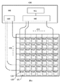
図1に示す能動タッチシステム100は、タッチ基板110と、能動デバイスアレイ120と、タッチ電極と、タッチ回路140と、などを備える。3端子能動デバイスアレイ120とタッチ電極は、タッチ基板110に設置されている。タッチ電極は、センサー電極アレイ131と、交差する2群の行制御電極132及び列検出電極133とから構成され、各制御電極線と各検出電極線との交差する箇所において絶縁層で隔てられている。タッチ基板110は透明基板であり、センサー電極アレイ131の各センサー電極ユニットは透明ITO電極であり、センサー電極アレイ131、行制御電極132及び列検出電極133はいずれもユーザに向かっていない非タッチ面に設置されており、センサー電極アレイ131、行制御電極132及び列検出電極133には1層の絶縁的な保護外層が更に設置されている。タッチ回路140は、タッチ励起源141と、信号検出回路142と、制御回路143とを有する。
An
制御電極132と検出電極133における各制御電極線と各検出電極線は、それぞれ3端子能動デバイスアレイ120における各能動デバイスユニットの2つの端子に接続されている。センサー電極アレイ131における各センサー電極ユニットは、それぞれ各能動デバイスユニットの他方の端子に接続されている。検出電極133はタッチ回路140におけるタッチ励起源141と信号検出回路142に接続されている。制御電極132はタッチ回路140における制御回路143に接続されている。
Each control electrode line and each detection electrode line in the
タッチ回路140のタッチ励起源141は、検出電極133の各検出電極線にタッチ信号を同時に与える。タッチ回路140の制御回路143は、走査により、1行ずつ制御電極132の各制御電極線にオン信号を出力し、オン信号を有する制御電極線に接続される能動デバイスユニットはオン状態になり、オン信号を有しない制御電極線に接続される能動デバイスユニットはオフ状態になる。制御回路143は、1行の制御電極線における能動デバイスユニットをオン状態にするごとに、各検出電極線におけるタッチ信号は能動デバイスユニットを介して当該行制御電極線に接続されるセンサー電極ユニット内に流れ込む。タッチ回路140の信号検出回路142は、各々の検出電極線におけるタッチ信号の変化の大きさを同時に検出し、又は、各々の検出電極線におけるタッチ信号の変化の大きさを1列ずつ検出する。このように、制御回路143は1行ずつ各制御電極線にオン信号を出力するに従って、信号検出回路142は、能動デバイスユニットを介して当該行制御電極線に接続されるセンサー電極ユニットにおけるタッチ信号の変化の大きさを1行ずつ検出する。
The
作業者の指又は他のタッチ物は、あるセンサー電極ユニットに近接又は接触すると、指又は他のタッチ物とセンサー電極ユニットとの間に結合容量が形成され、センサー電極ユニットにおけるタッチ信号はこの結合容量部分を介して漏洩される。信号検出回路142は、センサー電極ユニットにタッチ信号を与える各々の検出電極線におけるタッチ信号の変化の大きさを検出することにより、リーク電流が最大であり、又はリーク電流がある閾値を超えた検出電極線を見出すことができる。更に、この時、能動デバイスの制御電極線をオンにすることにより、リーク電流が生じたセンサー電極ユニットを決定することができる。これにより、タッチ基板110における指又は他のタッチ物の位置を見出すことができる。能動タッチシステム100は、タッチポイントの位置を検出可能なタッチシステムになる。
When an operator's finger or other touch object approaches or comes into contact with a certain sensor electrode unit, a coupling capacitance is formed between the finger or other touch object and the sensor electrode unit, and the touch signal in the sensor electrode unit is coupled to this sensor electrode unit. Leaked through the capacitive part. The
作業者の複数の指又は複数の作業者の指は、それぞれタッチ基板110における複数の位置をタッチすると、信号検出回路142は、複数の時点での複数本の検出電極線において、タッチ信号の変化がある閾値を超えたことを検出し、つまり、複数のセンサー電極ユニットのリーク電流がある閾値を超えたことを検出し、これにより、タッチ基板110における複数の指のそれぞれの位置を見出す。能動タッチシステム100は、複数のタッチポイントを識別可能なタッチシステムにもなる。
When the plurality of fingers of the worker or the fingers of the plurality of workers respectively touch a plurality of positions on the
実施形態2
図2に示す能動タッチシステム200は、タッチ基板210と、薄膜トランジスタ(TFT)アレイ220と、タッチ電極と、タッチ回路240と、などを備える。薄膜トランジスタ(TFT)アレイ220とタッチ電極は、タッチ基板210に設置されている。タッチ電極は、センサー電極アレイ231と、交差する2群の行制御電極232及び列検出電極233とから構成され、各制御電極線と各検出電極線との交差する箇所において絶縁層で隔てられている。タッチ基板210は透明基板であり、センサー電極アレイ231の各センサー電極ユニットは透明ITO電極であり、センサー電極アレイ231、行制御電極232、及び列検出電極233は、いずれもユーザに向かうタッチ面に設置されており、センサー電極アレイ231、行制御電極232、及び列検出電極233には、1層の絶縁的な保護外層が更に設置されている。タッチ回路240は、タッチ励起源241と、信号検出回路242と、制御回路243とを有する。
Embodiment 2
An
制御電極232と検出電極233における各制御電極線と各検出電極線は、それぞれTFTアレイ220の各TFTのゲートとソースに接続されている。センサー電極アレイ231の各センサー電極ユニットはそれぞれ各TFTのドレインに接続されている。検出電極233はタッチ回路240におけるタッチ励起源241と信号検出回路242に接続されている。制御電極232はタッチ回路240における制御回路243に接続されている。
Each control electrode line and each detection electrode line in the
タッチ回路240のタッチ励起源241は、検出電極233の各検出電極線にタッチ信号を同時に与える。タッチ回路240の制御回路243は、走査により、1行ずつ制御電極232の各制御電極線にオン信号を出力し、オン信号を有する制御電極線に接続されるTFTはオン状態になり、オン信号を有しない制御電極線に接続されるTFTはオフ状態になる。制御回路243は、1行の制御電極線におけるTFTをオン状態にするごとに、各検出電極線におけるタッチ信号は、TFTを介して当該行制御電極線に接続されるセンサー電極ユニット内に流れ込む。タッチ回路240における信号検出回路242は、各々の検出電極線におけるタッチ信号の変化の大きさを同時に検出し、又は、各々の検出電極線におけるタッチ信号の変化の大きさを1列ずつ検出する。このように、制御回路243は、1行ずつ各制御電極線にオン信号を出力するに従って、信号検出回路242は、TFTを介して当該行制御電極線に接続されるセンサー電極ユニットにおけるタッチ信号の変化の大きさを1行ずつ検出する。
The
作業者の指又は他のタッチ物は、あるセンサー電極ユニットに近接又は接触すると、指又は他のタッチ物とセンサー電極ユニットとの間に結合容量が形成され、センサー電極ユニットにおけるタッチ信号は、この結合容量部分を介して漏洩される。信号検出回路242は、センサー電極にタッチ信号を与える各々の検出電極線におけるタッチ信号の変化の大きさを検出することにより、リーク電流が最大であり、又はリーク電流がある閾値を超えた検出電極線を見出すことができる。更に、この時、TFTの制御電極線をオンにすることにより、リーク電流が生じたセンサー電極ユニットを決定することができる。これにより、タッチ基板210における指又は他のタッチ物の位置を見出すことができる。能動タッチシステム200は、タッチポイントの位置を検出可能なタッチシステムになる。
When an operator's finger or other touch object approaches or comes into contact with a certain sensor electrode unit, a coupling capacitance is formed between the finger or other touch object and the sensor electrode unit. It leaks through the coupling capacitance part. The
作業者の複数の指又は複数の作業者の指は、それぞれタッチ基板210における複数の位置をタッチすると、信号検出回路242は、複数の時点での複数本の検出電極線において、タッチ信号の変化がある閾値を超えたことを検出し、つまり、複数のセンサー電極ユニットのリーク電流がある閾値を超えたことを検出し、これにより、タッチ基板210における複数の指のそれぞれの位置を見出す。能動タッチシステム200は、複数のタッチポイントを識別可能なタッチシステムにもなる。
When the plurality of fingers of the worker or the fingers of the plurality of workers respectively touch a plurality of positions on the
実施形態3
図3に示す能動タッチシステム300は、タッチ基板310と、能動デバイスアレイ320と、タッチ電極と、タッチ回路340と、などを備える。2端子能動デバイスアレイ320とタッチ電極は、タッチ基板310に設置されている。タッチ電極は、センサー電極アレイ331と、交差する2群の行制御電極332及び列検出電極333とから構成され、各制御電極線と各検出電極線との交差する箇所において絶縁層で隔てられている。タッチ基板310は、フレキシブル透明基板であり、センサー電極アレイ331の各センサー電極ユニットは透明ITO電極であり、センサー電極アレイ331、行制御電極332、及び列検出電極333は、いずれもユーザに向かっていない非タッチ面に設置されている。タッチ回路340は、タッチ励起源341と、信号検出回路342と、制御回路343とを有する。
The
制御電極332における各制御電極線は、それぞれ1つのコンデンサを介してセンサー電極アレイ331の各センサー電極ユニットに接続され、各センサー電極ユニットは、更にそれぞれ2端子能動デバイスアレイ320の各能動デバイスユニットの他方の端子に接続される。検出電極333の各検出電極線は、それぞれ2端子能動デバイスアレイ320の各能動デバイスユニットの他方の端子に接続される。検出電極333は、タッチ回路340におけるタッチ励起源341と信号検出回路342に接続される。制御電極332は、タッチ回路340における制御回路343に接続される。
Each control electrode line in the
タッチ回路340のタッチ励起源341は、検出電極333の各検出電極線にタッチ信号を同時に与える。タッチ回路340の制御回路343は、走査により、制御電極332の各制御電極線にオン信号を1行ずつ出力し、オン信号は、コンデンサやセンサー電極ユニットを介してオン信号を有する制御電極線に接続される能動デバイスユニットをオン状態にし、オン信号を有しない制御電極線に接続される能動デバイスユニットをオフ状態にする。制御回路343は、1行の制御電極線における能動デバイスユニットをオン状態にするごとに、各検出電極線におけるタッチ信号は、当該行制御電極線に接続されるセンサー電極ユニット内に流れ込む。タッチ回路340の信号検出回路342は、各々の検出電極線におけるタッチ信号の変化の大きさを同時に検出し、又は、各々の検出電極線におけるタッチ信号の変化の大きさを1列ずつ検出する。このように、制御回路343は、1行ずつ各制御電極線にオン信号を出力するに従って、信号検出回路342は、当該行制御電極線でのセンサー電極ユニットにおけるタッチ信号の変化の大きさを1行ずつ検出する。
The
作業者の指又は他のタッチ物は、あるセンサー電極ユニットに近接又は接触すると、指又は他のタッチ物はセンサー電極ユニットとの間に結合容量が形成され、センサー電極ユニットにおけるタッチ信号はこの結合容量部分を介して漏洩される。信号検出回路342は、センサー電極ユニットにタッチ信号を与える検出電極線の各々におけるタッチ信号の変化の大きさを検出することにより、リーク電流が最大であり、又はリーク電流がある閾値を超えた検出電極線を見出すことができる。更に、この時、能動デバイスの制御電極線をオンにすることにより、リーク電流が生じたセンサー電極ユニットを決定することができる。これにより、タッチ基板310における指又は他のタッチ物の位置を見出すことができる。能動タッチシステム300は、タッチポイントの位置を検出可能なタッチシステムになる。
When an operator's finger or other touch object approaches or comes into contact with a certain sensor electrode unit, a coupling capacitance is formed between the finger or other touch object and the sensor electrode unit, and the touch signal in the sensor electrode unit is coupled to this sensor electrode unit. Leaked through the capacitive part. The
作業者の複数の指又は複数の作業者の指は、それぞれタッチ基板310における複数の位置をタッチすると、信号検出回路342は、複数の時点での複数本の検出電極線において、タッチ信号の変化がある閾値を超えたことを検出し、つまり、複数のセンサー電極ユニットのリーク電流がある閾値を超えたことを検出し、これにより、タッチ基板310における複数の指のそれぞれの位置を見出す。能動タッチシステム300は、複数のタッチポイントを識別可能なタッチシステムになる。
When the plurality of fingers of the worker or the fingers of the plurality of workers touch the plurality of positions on the
実施形態4
図4に示す能動タッチシステム400は、タッチ基板410と、能動デバイスアレイ420と、タッチ電極と、タッチ回路440と、などを備える。能動デバイスユニットアレイ420とタッチ電極は、タッチ基板410に設置されており、それぞれの能動デバイスユニットは、1つのダイオードと、1つのコンデンサとを直列接続してなるものである。タッチ電極は、センサー電極アレイ431と、交差する2群の行制御電極432及び列検出電極433とから構成され、各制御電極線と各検出電極線との交差する箇所において絶縁層で隔てられている。タッチ基板410はフレキシブル透明基板であり、センサー電極アレイ431の各センサー電極ユニットは透明ITO電極であり、センサー電極アレイ431、行制御電極432、及び列検出電極433は、いずれもユーザに向かっていない非タッチ面に設置されている。タッチ回路440は、タッチ励起源441と、信号検出回路442と、制御回路443とを有する。
An
制御電極432及び検出電極433における各制御電極線及び各検出電極線は、それぞれ能動デバイスアレイ420の各ダイオード及びコンデンサ直列接続ユニットの2つの端子に接続されている。センサー電極アレイ431の各センサー電極ユニットは、それぞれ各ダイオードとコンデンサとの間の接続点に接続されている。検出電極433は、タッチ回路440におけるタッチ励起源441と信号検出回路442とに接続されている。制御電極432は、タッチ回路440における制御回路443に接続されている。
Each control electrode line and each detection electrode line in the
タッチ回路440のタッチ励起源441は、検出電極433の各検出電極線にタッチ信号を同時に与える。タッチ回路440の制御回路443は、走査により、制御電極432の各制御電極線にオン信号を1行ずつ出力し、オン信号を有する制御電極線に接続されるダイオード及びコンデンサ直列接続ユニットはオン状態になり、オン信号を有しない制御電極線に接続されるダイオード及びコンデンサ直列接続ユニットはオフ状態になる。制御回路443は、1行の制御電極線における能動デバイスユニットをオン状態にするごとに、各検出電極線におけるタッチ信号は、当該行制御電極線に接続されるセンサー電極ユニット内に流れ込む。タッチ回路440の信号検出回路442は、各々の検出電極線におけるタッチ信号の変化の大きさを同時に検出し、又は、各々の検出電極線におけるタッチ信号の変化の大きさを1列ずつ検出する。このように、制御回路443は、1行ずつ各制御電極線にオン信号を出力するに従って、信号検出回路442は、当該行制御電極線におけるセンサー電極ユニットにおけるタッチ信号の変化の大きさを1行ずつ検出する。
The
作業者の指又は他のタッチ物は、あるセンサー電極ユニットに近接又は接触すると、指又は他のタッチ物とセンサー電極ユニットとの間に結合容量が形成され、センサー電極ユニットにおけるタッチ信号は、この結合容量部分を介して漏洩される。信号検出回路442は、センサー電極ユニットにタッチ信号を与える検出電極線の各々におけるタッチ信号の変化の大きさを検出することにより、リーク電流が最大であり、又はリーク電流がある閾値を超えた検出電極線を見出すことができる。更に、この時、能動デバイスユニットの制御電極線をオンにすることにより、リーク電流が生じたセンサー電極ユニットを決定することができ、これにより、タッチ基板410における指又は他のタッチ物の位置を見出す。能動タッチシステム400は、タッチポイントの位置を検出可能なタッチシステムになる。
When an operator's finger or other touch object approaches or comes into contact with a certain sensor electrode unit, a coupling capacitance is formed between the finger or other touch object and the sensor electrode unit. It leaks through the coupling capacitance part. The
作業者の複数の指又は複数の作業者の指は、それぞれタッチ基板410における複数の位置をタッチすると、信号検出回路442は、複数の時点での複数本の検出電極線において、タッチ信号の変化がある閾値を超えたことを検出し、つまり、複数のセンサー電極ユニットのリーク電流がある閾値を超えたことを検出し、これにより、タッチ基板410における複数の指のそれぞれの位置を見出す。能動タッチシステム400は、複数のタッチポイントを識別可能なタッチシステムになる。
When the plurality of fingers of the worker or the fingers of the plurality of workers respectively touch a plurality of positions on the
実施形態5
図5に示す能動タッチシステム500は、タッチ基板510と、薄膜トランジスタ(TFT)アレイ520と、タッチ電極と、タッチ回路540と、表示スクリーンと、などを備える。薄膜トランジスタ(TFT)アレイ520とタッチ電極は、タッチ基板510に設置されている。タッチ電極は、センサー電極アレイ531と、交差する2群の行制御電極532及び列検出電極533とから構成され、各制御電極線と各検出電極線との交差する箇所において絶縁層で隔てられている。タッチ基板510における全ての列検出電極533の位置がユーザに向かう側の異なる層には、タッチ物と検出電極533との相互作用が抑止されるように、線状の遮蔽電極534が設置されている。タッチ基板510のユーザに向かっていない側の異なる層には、表示スクリーンにおける電気信号によるセンサー電極アレイ531と検出電極533に対するタッチ信号の影響が抑止されるように、面状の遮蔽電極535が設置されている。遮蔽電極534、535と検出電極533、制御電極532とTFTアレイ520は、絶縁層で隔てられている。タッチ基板510は共用表示スクリーンにおける1つの基板であり、センサー電極アレイ531の各センサー電極ユニットは透明ITO電極であり、センサー電極アレイ531、行制御電極532及び列検出電極533は、いずれもユーザに向かうタッチ面に設置されており、センサー電極アレイ531、行制御電極532、及び列検出電極533には、1層の絶縁的な保護外層が更に設置されている。タッチ回路540は、タッチ励起源541と、信号検出回路542と、制御回路543とを有する。
Embodiment 5
An
制御電極532と検出電極533における各制御電極線と各検出電極線は、それぞれTFTアレイ520の各TFTのゲートとソースに接続されている。センサー電極アレイ531の各センサー電極ユニットは、それぞれ各TFTのドレインに接続されている。検出電極533は、タッチ回路540におけるタッチ励起源541と信号検出回路542に接続されている。遮蔽電極534と遮蔽電極535は互いに連通されていると共に、タッチ回路540のグランドに接続されている。
Each control electrode line and each detection electrode line in the
タッチ回路540のタッチ励起源541は、検出電極533の各検出電極線にタッチ信号を同時に与える。タッチ回路540の制御回路543は、走査により、制御電極532の各制御電極線にオン信号を1行ずつ出力し、オン信号を有する制御電極線に接続されるTFTはオン状態になり、オン信号を有しない制御電極線に接続されるTFTはオフ状態になる。制御回路543は、1行の制御電極線におけるTFTをオン状態にするごとに、各検出電極線におけるタッチ信号は、TFTを介して当該行制御電極線に接続されるセンサー電極ユニット内に流れ込む。タッチ回路540の信号検出回路542は、各々の検出電極線におけるタッチ信号の変化の大きさを同時に検出し、又は、各々の検出電極線におけるタッチ信号の変化の大きさを1列ずつ検出する。このように、制御回路543は、1行ずつ各制御電極線にオン信号を出力するに従って、信号検出回路542は、TFTを介して当該行制御電極線に接続されるセンサー電極ユニットにおけるタッチ信号の変化の大きさを1行ずつ検出する。
The
作業者の指又は他のタッチ物はあるセンサー電極ユニットに近接又は接触すると、指又は他のタッチ物とセンサー電極ユニットとの間に結合容量が形成され、センサー電極ユニットにおけるタッチ信号は、この結合容量部分を介して漏洩される。遮蔽電極534と遮蔽電極535が設置されているため、指又は他のタッチ物と検出電極533との間にリーク電流を発生させる結合容量がなく、ディスプレイにおける電気信号がセンサー電極アレイ531と検出電極533におけるタッチ信号に対して影響を与えることもない。信号検出回路542は、センサー電極ユニットにタッチ信号を与える検出電極線の各々におけるタッチ信号の変化の大きさを検出することにより、リーク電流が最大であり、又はリーク電流がある閾値を超えた検出電極線を見出すことができる。更に、この時、TFTの制御電極線をオンにすることにより、リーク電流が生じたセンサー電極ユニットを決定することができる。これにより、タッチ基板510における指又は他のタッチ物の位置を見出す。能動タッチシステム500は、タッチポイントの位置を検出可能なタッチシステムになる。
When an operator's finger or other touch object approaches or comes into contact with a certain sensor electrode unit, a coupling capacitance is formed between the finger or other touch object and the sensor electrode unit. Leaked through the capacitive part. Since the shielding electrode 534 and the shielding electrode 535 are provided, there is no coupling capacitance that generates a leakage current between the finger or other touch object and the
作業者の複数の指又は複数の作業者の指は、それぞれタッチ基板510における複数の位置をタッチすると、信号検出回路542は、複数の時点での複数本の検出電極線において、タッチ信号の変化がある閾値を超えたことを検出し、つまり、複数のセンサー電極ユニットのリーク電流がある閾値を超えたことを検出し、これにより、タッチ基板510における複数の指のそれぞれの位置を見出す。能動タッチシステム500は、複数のタッチポイントを識別可能なタッチシステムになる。
When the plurality of fingers of the worker or the fingers of the plurality of workers respectively touch a plurality of positions on the
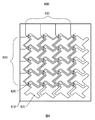
実施形態6
図6に示す能動タッチシステム600は、タッチ基板610と、薄膜トランジスタ(TFT)アレイ620と、タッチ電極と、などを備える。TFTアレイ620とタッチ電極は、タッチ基板610に設置されている。タッチ電極は、センサー電極アレイ631と、交差する2群の行制御電極632及び列検出電極633とから構成され、各制御電極線と各検出電極線との交差する箇所において絶縁層で隔てられている。タッチ基板610は透明基板であり、センサー電極アレイ631における各センサー電極ユニットは透明ITO電極であり、行制御電極632と列検出電極633とは不透明な金属電極線である。
Embodiment 6
An
能動タッチスクリーン600と表示スクリーンとを積層して使用する場合に、不透明な行電極線と列電極線、及び透明なセンサー電極のエッジによる表示効果に対する影響を抑止するために、有効なタッチ領域において行電極線と列電極線を折れ線にし、前記折れ線において隣接する2本の直線の夾角を20°より大きく、且つ160°より小さくし、また、行電極線と列電極線とが交差しているが重複部分がないようにする。透明なセンサー電極ユニットのエッジ形状は、隣接する2本の行電極線と隣接する2本の列電極線に沿って囲まれた多角形になるようにする。行制御電極632と列検出電極633は、それらの交差する箇所において、TFTアレイ620及びセンサー電極アレイ631により接続されている。能動タッチスクリーン600が表示スクリーンと組合せて使用される場合に、不透明な行電極632と列電極633における傾斜線分は表示スクリーンにおける不透明な表示行列電極と回折縞を形成しなく、透明なセンサー電極631の折れ線エッジは、表示スクリーンにおける透明な表示画素電極と干渉縞を形成しないため、表示品質に対する影響が極力防止される。
In the case where the
実施形態7
図7に示す能動タッチシステム700は、タッチ基板710と、能動デバイスアレイ720と、タッチ電極と、タッチ回路740と、などを備える。3端子能動デバイスアレイ720とタッチ電極は、タッチ基板710に設置されている。タッチ電極は、センサー電極アレイ731と、交差する2群の行制御電極732及び列検出電極733とから構成され、各制御電極線と各検出電極線との交差する箇所において絶縁層で隔てられている。タッチ基板710は透明基板であり、センサー電極アレイ731の各センサー電極ユニットは透明ITO電極であり、センサー電極アレイ731、行制御電極732、及び列検出電極733は、いずれもユーザに向かっていない非タッチ面に設置されており、センサー電極アレイ731、行制御電極732、及び列検出電極733には、1層の絶縁的な保護外層が更に設置されている。タッチ回路740は、第1の出力端7411及び第2の出力端7412を有するタッチ励起源741と、タッチ信号サンプリング素子7421と、バッファロー、差動増幅回路、データサンプリングチャンネル、データ処理、及びタイミングコントローラ等の回路からなる検出回路における他の回路7422とを含む信号検出回路742と、制御回路743とを備える。
Embodiment 7
An
制御電極732と検出電極733における各制御電極線と各検出電極線は、それぞれ3端子能動デバイスアレイ720における各能動デバイスユニットの2つの端子に接続されている。センサー電極アレイ731の各センサー電極ユニットは、それぞれ各能動デバイスユニットの他方の端子に接続されている。検出電極733における733i電極線は、タッチ信号サンプリング素子7421を介してタッチ励起源の第1の出力端7411に接続され、検出電極733における電極線733i−1、733i+1は、タッチ励起源の第2の出力端7412に接続され、検出電極733における他の電極線もタッチ励起源の出力端7411に接続され、タッチ励起源における第1の出力端7411と第2の出力端7412とは同一のタッチ励起源における信号回流のための入出力端である。
Each control electrode line and each detection electrode line in the
タッチ回路740のタッチ励起源741は、検出電極733における各検出電極線にタッチ信号を同時に与える。タッチ回路740の制御回路743は、走査により、制御電極732の各制御電極線にオン信号を1行ずつ出力し、オン信号を有する制御電極線に接続される能動デバイスユニットはオン状態になり、オン信号を有しない制御電極線に接続される能動デバイスユニットはオフ状態になる。制御回路743は1行の制御電極線における能動デバイスユニットをオン状態にするごとに、各検出電極線におけるタッチ信号は能動デバイスユニットを介して当該行制御電極線に接続されるセンサー電極ユニットに流れ込む。センサー電極ユニット731jiとセンサー電極ユニット731ji−1との間に、結合容量Ci−1が形成され、センサー電極ユニット731jiとセンサー電極ユニット731ji−1との間に、結合容量Ci+1が形成される。タッチ信号は、タッチ励起源741と、検出電極線733iと、センサー電極ユニット731jiと、結合容量Ci−1と、センサー電極ユニット731ji−1と、検出電極線733i−1との間に閉鎖回路を形成し、タッチ励起源741と、検出電極線733iと、センサー電極ユニット731jiと、結合容量Ci+1と、センサー電極ユニット731ji+1と、検出電極線733i+1との間に閉鎖回路も形成する。タッチ励起源741の第1の出力端7411から流れ出したタッチ信号は、タッチ信号サンプリング素子7421を介して検出電極線733iに流れ込み、そして、それぞれ結合容量Ci−1と結合容量Ci+1を介してセンサー電極ユニット731ji−1とセンサー電極ユニット731ji+1に流れ込んだ後、検出電極733i−1と検出電極733i−1を介してタッチ励起源741の第2の出力端7412に還流するように、タッチ信号が閉鎖したタッチ回路において流れる。
The
タッチ物である人の指は検出電極線733iに近接又は接触すると、指に一定の幅があるため、センサー電極ユニット731ji、センサー電極ユニット731ji−1、及びセンサー電極ユニット731jiを同時にタッチし、人体の誘電係数が空気の誘電係数よりずっと大きいので、結合容量Ci−1とCi+1の容量値が増大すると共に容量性リアクタンスが減少し、タッチ回路におけるタッチ信号の電流は相応して大きくなる。指が733i、733i−1及び733i+1ではない他の検出電極線の位置に近接又は接触すると、検出電極線同士の間、センサー電極ユニット同士の間、センサー電極ユニットと検出電極線との間の結合容量のいずれも変更されることになるが、タッチ位置において各電極に連通されるタッチ励起源741の出力端が全て同一の出力端7411であるため、タッチ信号サンプリング素子7421を流れているタッチ信号電流の変化は非常に小さい。
When the finger of a person who is a touched object approaches or touches the detection electrode line 733i, the finger has a certain width. Is much larger than the dielectric coefficient of air, the capacitance values of the coupling capacitors C i−1 and C i + 1 increase and the capacitive reactance decreases, and the current of the touch signal in the touch circuit increases correspondingly. When a finger approaches or touches the position of another detection electrode line that is not 733i, 733i-1, and 733i + 1, the coupling between the detection electrode lines, between the sensor electrode units, and between the sensor electrode unit and the detection electrode line Although all of the capacities are changed, since the output ends of the
信号検出回路742は、走査により、センサー電極ユニットにタッチ信号を与える各々の検出電極線におけるタッチ信号の変化の大きさを1本ずつ検出することにより、電流変化が最大であり、又は電流変化がある閾値を超えた検出電極線を見出すことができる。更に、この時、能動デバイスの制御電極線をオンにすることにより、タッチされたセンサー電極ユニットを決定することができる。これにより、タッチ基板710における指又は他のタッチ物の位置を見出す。能動タッチシステム700は、タッチポイントの位置を検出可能なタッチシステムになる。
The
検出電極を複数の領域に分け、異なる領域において前記と同様な原理に従ってタッチ励起信号を加えて検出を行うことにより、タッチ検出の速度を向上させてもよい。作業者の複数の指又は複数の作業者の指はそれぞれタッチ基板710における複数の位置をタッチすると、信号検出回路742は複数の時点での複数本の検出電極線において、タッチ信号の変化がある閾値を超えたことを検出し、つまり、複数のセンサー電極ユニットの電流変化がある閾値を超えたことを検出し、これにより、タッチ基板710における複数の指のそれぞれの位置を見出す。能動タッチシステム700は、複数のタッチポイントを識別可能なタッチシステムになる。
The speed of touch detection may be improved by dividing the detection electrode into a plurality of regions and performing detection by applying a touch excitation signal in different regions according to the same principle as described above. When the plurality of fingers of the worker or the fingers of the plurality of workers respectively touch a plurality of positions on the
実施形態8
図8に示す能動タッチシステム800は、タッチ基板810と、薄膜トランジスタ(TFT)アレイ820と、タッチ電極と、タッチ回路840と、などを備える。薄膜トランジスタ(TFT)アレイ820とタッチ電極は、タッチ基板810に設置されている。検出電極は、センサー電極アレイ831と、交差する2群の行制御電極832及び列検出電極833とから構成され、各制御電極線と各検出電極線との交差する箇所において絶縁層で隔てられている。タッチ基板810は透明基板であり、センサー電極アレイ831の各センサー電極ユニットは透明ITO電極であり、センサー電極アレイ831、行制御電極832及び列検出電極833はいずれもユーザに向かうタッチ面に設置されており、センサー電極アレイ831、行制御電極832、及び列検出電極833には、1層の絶縁的な保護外層が更に設置されている。タッチ回路840は、タッチ信号の第1の出力端8411及び第2の出力端8412を有するタッチ励起源841と、タッチ信号サンプリング素子8421、バッファロー、差動増幅回路、データサンプリングチャンネル、データ処理、及びタイミングコントローラ等の回路などを有する信号検出回路842と、制御回路843とを備え、能動タッチシステムはアウターケーシング850を有する。
An
制御電極832と検出電極833における各制御電極線と各検出電極線は、それぞれTFTアレイ820の各TFTのゲートとソースに接続されている。センサー電極アレイ831の各センサー電極ユニットはそれぞれ各TFTのドレインに接続されている。検出電極833は、タッチ回路840におけるタッチ励起源841と信号検出回路842に接続されている。制御電極832は、タッチ回路840における制御回路843に接続されている。アウターケーシングには電極851が設置されている。
Each control electrode line and each detection electrode line in the
タッチ回路840のタッチ励起源841の第1の出力端8411は、検出電極833の各検出電極線にタッチ信号を同時に出力し、アウターケーシング電極851は、タッチ信号の還流電極として、タッチ励起源841の第2の出力端8412に接続される。タッチ回路840における制御回路843は、走査により、1行ずつ制御電極832の各制御電極線にオン信号を出力し、オン信号を有する制御電極線に接続されるTFTはオン状態になり、オン信号を有しない制御電極線に接続されるTFTはオフ状態になる。制御回路843は、1行の制御電極線におけるTFTをオン状態にするごとに、各検出電極線におけるタッチ信号はTFTを介して当該行制御電極線に接続されるセンサー電極ユニット内に流れ込む。タッチ回路840の信号検出回路842は、各々の検出電極線におけるタッチ信号の変化の大きさを同時に検出し、又は、各々の検出電極線におけるタッチ信号の変化の大きさを1列ずつ検出する。このように、制御回路843は、1行ずつ各制御電極線にオン信号を出力するに従って、信号検出回路842は、TFTを介して当該行制御電極線に接続されるセンサー電極ユニットにおけるタッチ信号の変化の大きさを1行ずつ検出する。
The
人の指は、検出電極833におけるある1本の電極線833iと制御電極832におけるある1本の電極線832jに接続されるセンサー電極ユニット831jiに近接又は接触すると、指とセンサー電極ユニット831jiの間に1つの結合容量Ciが生じ、タッチ励起源841の第1の出力端8411によりタッチ信号サンプリング素子8421を介して検出電極線833iに出力されたタッチ励起信号は、オン信号のTFTを介してセンサー電極ユニット831jiに流れ込み、そして、この結合容量Ciを介して指に流れ込み、製品を持っている手のひらを介して製品のアウターケーシングにおける還流電極851に流れ込み、更に還流電極851からタッチ励起源841の第2の出力端8412に還流する。タッチ励起源、タッチ検出電極線、センサー電極ユニット、指とセンサー電極ユニットとの間の結合容量、及びアウターケーシングにおける還流電極により、タッチ回路が構成される。タッチ信号がタッチシステムの間にクロストークすることが抑止されるように、オン信号がない制御電極線をタッチ信号の第1の出力端に接続させてもよい。
When a human finger approaches or comes into contact with a sensor electrode unit 831ji connected to a certain electrode line 833i of the
タッチ信号サンプリング素子8421を流れているタッチ信号の電流の変化を同時又は1本ずつに検出することにより、電流変化が最大であり、又は電流の変化がある閾値を超えた検出電極線を見出すことができる。更に、この時、能動デバイスの制御電極線をオンにすることにより、タッチされたセンサー電極ユニットを決定することができる。これにより、タッチ基板810における指又は他のタッチ物の位置を見出す。能動タッチシステム800は、タッチポイントの位置を検出可能なタッチシステムになる。
By detecting a change in the current of the touch signal flowing through the touch
以上、具体的な好ましい実施形態と合わせて本発明を更に詳細に説明したが、本発明の具体的な実施がそれらの説明に限定されると思うべきではない。当業者にとっては、本発明の趣旨を逸脱することなく、さらに幾つかの簡単な推理・演繹又は置換を行うことができ、これらは本発明の保護範囲に属すると考えるべきである。 While the present invention has been described in further detail in conjunction with specific preferred embodiments, it should not be construed that the specific implementation of the invention is limited to those descriptions. For those skilled in the art, some simple reasoning, deduction or substitution can be made without departing from the spirit of the present invention, and these should be considered to be within the protection scope of the present invention.
Claims (16)
前記タッチ基板は、能動デバイスユニットがアレイ配列された能動デバイスユニットアレイ、前記センサー電極ユニットがアレイ配列されたセンサー電極ユニットアレイ、及び制御電極の群と検出電極の群とを少なくとも含む電極群を備え、
前記制御電極の各々から延びる制御電極線と前記検出電極の各々から延びる検出電極線とは各々交差し、交差する箇所は絶縁層で隔てられており、
前記センサー電極ユニットは前記能動デバイスユニットに接続され、前記能動デバイスユニットは前記制御電極と前記検出電極に接続され、
前記能動デバイスユニットアレイの前記能動デバイスユニットは、前記制御電極を介してオン・オフを制御され、
一部の能動デバイスユニットが、オン状態になると、全て又は一部の前記検出電極がタッチ信号を前記センサー電極ユニットに供給して、
作業者の指又は他のタッチ物が、前記センサー電極ユニットに近接又は接触すると、結合容量が、前記指又は他のタッチ物と、前記センサー電極ユニットとの間に形成されて、
前記センサー電極ユニットと連通されている前記検出電極上の前記タッチ信号の変化を検出して、タッチ物への前記センサー電極ユニットのリーク電流を検出して、
前記リーク電流を生じさせている前記センサー電極ユニットを決定することによって、前記タッチ基板上の前記指又は他のタッチ物の位置を決定することを特徴とする能動タッチシステム。 In an active touch system comprising a touch substrate, a sensor electrode unit , a control electrode and a detection electrode, the touch electrode for detecting the position of an operator's finger or other touch object on the touch substrate,
The touch substrate includes an active device unit array active device unit are arrayed sequences, the sensor electrode unit is a sensor electrode unit array are arrayed sequences, and including at least the electrode group and the group of the group and the detection electrode of the control electrode ,
The control electrode line extending from each of the control electrodes and the detection electrode line extending from each of the detection electrodes intersect each other, and the intersecting portions are separated by an insulating layer,
The sensor electrode unit is connected to the active device unit, the active device unit is connected to the control electrode and the detection electrode ;
The active device unit of the active device unit array is controlled on / off via the control electrode,
When some active device units are turned on, all or some of the detection electrodes supply a touch signal to the sensor electrode unit,
When an operator's finger or other touch object approaches or comes into contact with the sensor electrode unit, a coupling capacitance is formed between the finger or other touch object and the sensor electrode unit.
Detecting a change in the touch signal on the detection electrode communicated with the sensor electrode unit, detecting a leak current of the sensor electrode unit to a touch object,
An active touch system , wherein the position of the finger or other touch object on the touch substrate is determined by determining the sensor electrode unit causing the leakage current .
前記タッチ基板には、
能動デバイスユニットがアレイ配列された能動デバイスユニットアレイと、
前記センサー電極ユニットがアレイ配列されたセンサー電極ユニットアレイと、
制御電極の群と検出電極の群とを少なくとも含む電極群と
を備えられ、
前記制御電極の各々から延びる制御電極線と前記検出電極の各々から延びる検出電極線とは交差し、交差する箇所において絶縁層で隔てられており、
前記センサー電極ユニットは前記能動デバイスユニットに接続され、
前記能動デバイスユニットは前記制御電極と前記検出電極とに接続され、
前記検出電極は前記タッチ回路におけるタッチ励起源と信号検出回路に接続され、
前記制御電極は前記タッチ回路における制御回路に接続され、
前記タッチ回路は、前記制御電極により前記能動デバイスユニットアレイにおける能動デバイスユニットのオン・オフを制御し、一部の能動デバイスユニットがオン状態になると、全て又は一部の検出電極線で前記センサー電極ユニットにタッチ信号を供給し、前記センサー電極ユニットに連通される検出電極線におけるタッチ信号の変化を検出することにより、タッチポイントの位置を決定して、
作業者の指又は他のタッチ物が、前記センサー電極ユニットに近接又は接触すると、結合容量が、前記指又は他のタッチ物と、前記センサー電極ユニットとの間に形成されて、
前記センサー電極ユニットと連通されている前記検出電極上の前記タッチ信号の変化を検出して、タッチ物への前記センサー電極ユニットのリーク電流を検出して、
前記リーク電流を生じさせている前記センサー電極ユニットを決定することによって、前記タッチ基板上の前記指又は他のタッチ物の位置を決定することを特徴とする能動タッチシステム。 A touch substrate, a touch electrode having a sensor electrode unit , a control electrode, and a detection electrode; and a touch circuit having a touch excitation source, a signal detection circuit, and a control circuit, wherein the touch electrode and the touch circuit are the touch substrate. In an active touch system that detects the position of the operator's finger or other touch object at
In the touch substrate,
An active device unit array in which active device units are arrayed; and
A sensor electrode unit array in which the sensor electrode units are arrayed;
An electrode group including at least a group of control electrodes and a group of detection electrodes,
The control electrode line extending from each of the control electrodes and the detection electrode line extending from each of the detection electrodes intersect with each other, and are separated by an insulating layer at the intersection.
The sensor electrode unit is connected to the active device unit;
The active device unit is connected to the control electrode and the detection electrode;
The detection electrode is connected to a touch excitation source and a signal detection circuit in the touch circuit;
The control electrode is connected to a control circuit in the touch circuit;
The touch circuit controls on / off of the active device units in the active device unit array by the control electrodes, and when some of the active device units are turned on, the sensor electrodes are all or part of the detection electrode lines. By supplying a touch signal to the unit and detecting a change in the touch signal in the detection electrode line communicated with the sensor electrode unit, the position of the touch point is determined ,
When an operator's finger or other touch object approaches or comes into contact with the sensor electrode unit, a coupling capacitance is formed between the finger or other touch object and the sensor electrode unit.
Detecting a change in the touch signal on the detection electrode communicated with the sensor electrode unit, detecting a leak current of the sensor electrode unit to a touch object,
An active touch system , wherein the position of the finger or other touch object on the touch substrate is determined by determining the sensor electrode unit causing the leakage current .
Applications Claiming Priority (3)
| Application Number | Priority Date | Filing Date | Title |
|---|---|---|---|
| CN200910166203.7 | 2009-08-12 | ||
| CN200910166203 | 2009-08-12 | ||
| PCT/CN2009/075970 WO2011017891A1 (en) | 2009-08-12 | 2009-12-24 | Active touch control system |
Publications (3)
| Publication Number | Publication Date |
|---|---|
| JP2013501983A JP2013501983A (en) | 2013-01-17 |
| JP2013501983A5 JP2013501983A5 (en) | 2013-02-28 |
| JP5633565B2 true JP5633565B2 (en) | 2014-12-03 |
Family
ID=43585878
Family Applications (1)
| Application Number | Title | Priority Date | Filing Date |
|---|---|---|---|
| JP2012524079A Active JP5633565B2 (en) | 2009-08-12 | 2009-12-24 | Active touch system |
Country Status (5)
| Country | Link |
|---|---|
| US (1) | US8698770B2 (en) |
| EP (1) | EP2392994A4 (en) |
| JP (1) | JP5633565B2 (en) |
| CN (1) | CN202013558U (en) |
| WO (1) | WO2011017891A1 (en) |
Families Citing this family (31)
| Publication number | Priority date | Publication date | Assignee | Title |
|---|---|---|---|---|
| US7920129B2 (en) | 2007-01-03 | 2011-04-05 | Apple Inc. | Double-sided touch-sensitive panel with shield and drive combined layer |
| JP5832772B2 (en) * | 2011-04-13 | 2015-12-16 | シャープ株式会社 | Touch panel, touch panel system, and electronic device |
| US9259904B2 (en) | 2011-10-20 | 2016-02-16 | Apple Inc. | Opaque thin film passivation |
| WO2013063722A1 (en) * | 2011-11-04 | 2013-05-10 | 智点科技(深圳)有限公司 | Mutual-capacitance-type active touch control system |
| WO2013075279A1 (en) * | 2011-11-21 | 2013-05-30 | 智点科技(深圳)有限公司 | Active touch control flat-panel display |
| US9753588B2 (en) * | 2012-02-27 | 2017-09-05 | Slim Hmi Technology | Display apparatus and touch sensing method thereof |
| CN102609597A (en) * | 2012-03-29 | 2012-07-25 | 中国电子科技集团公司第十三研究所 | Method for layout of compound semiconductor microwave power chip |
| FR2990020B1 (en) * | 2012-04-25 | 2014-05-16 | Fogale Nanotech | CAPACITIVE DETECTION DEVICE WITH ARRANGEMENT OF CONNECTION TRACKS, AND METHOD USING SUCH A DEVICE. |
| US9201547B2 (en) | 2012-04-30 | 2015-12-01 | Apple Inc. | Wide dynamic range capacitive sensing |
| TW201351245A (en) * | 2012-06-04 | 2013-12-16 | Wintek Corp | Touch-sensing electrode structure and touch-sensitive device |
| CN103631463B (en) * | 2012-08-24 | 2018-10-23 | 敦泰电子(深圳)有限公司 | A kind of digital capacitive touch panel |
| CN103677458B (en) * | 2012-09-17 | 2016-08-17 | 凌巨科技股份有限公司 | Touch-control system and inducing method thereof |
| US9417740B2 (en) * | 2013-01-03 | 2016-08-16 | Nokia Technologies Oy | Capacitive sensing apparatus with a shield electrode |
| KR20150108356A (en) * | 2013-01-24 | 2015-09-25 | 도판 인사츠 가부시키가이샤 | Touch panel and display device |
| WO2014145770A2 (en) * | 2013-03-15 | 2014-09-18 | Cirque Corporation | Flying sense electrodes for creating a secure cage for integrated circuits and pathways |
| TW201447704A (en) * | 2013-06-10 | 2014-12-16 | Ili Technology Corp | Touch panel with transparent conductive layer |
| CN103425347B (en) * | 2013-08-02 | 2018-01-02 | 敦泰电子有限公司 | Touch control display apparatus |
| CN104808869A (en) * | 2014-01-23 | 2015-07-29 | 天津富纳源创科技有限公司 | Detection method of contact point of touch screen |
| CN103970392B (en) * | 2014-04-18 | 2019-10-01 | 京东方科技集团股份有限公司 | A kind of touch screen and display device |
| CN105022520A (en) * | 2014-04-30 | 2015-11-04 | 群创光电股份有限公司 | Touch panel and touch display apparatus |
| KR102236314B1 (en) * | 2014-10-29 | 2021-04-05 | 삼성디스플레이 주식회사 | Touch display device for energy harvesting |
| WO2016074223A1 (en) * | 2014-11-14 | 2016-05-19 | Texas Instruments Incorporated | Capacitive touch sensing |
| CN104699322B (en) * | 2015-04-01 | 2017-12-29 | 上海天马微电子有限公司 | Array base palte, touch-control display panel, touch control display apparatus and detection method |
| DE102015107739A1 (en) * | 2015-05-18 | 2016-11-24 | Osram Opto Semiconductors Gmbh | Light source with multiple semiconductor components |
| JP6503275B2 (en) * | 2015-10-09 | 2019-04-17 | 株式会社ジャパンディスプレイ | Sensor and display device with sensor |
| CN114527893B (en) | 2016-09-23 | 2023-11-10 | 苹果公司 | Touch sensor panel with top shield and/or bottom shield |
| US10372282B2 (en) | 2016-12-01 | 2019-08-06 | Apple Inc. | Capacitive coupling reduction in touch sensor panels |
| US20200174640A1 (en) * | 2018-12-03 | 2020-06-04 | Wuhan China Star Optoelectronics Semiconductor Display Technology Co., Ltd. | Touch screen and display device |
| US10825384B2 (en) * | 2019-03-27 | 2020-11-03 | Wuhan China Star Optoelectronics Semiconductor Display Technology Co., Ltd. | Display panel and display device |
| CN111290662A (en) * | 2020-01-22 | 2020-06-16 | 京东方科技集团股份有限公司 | Touch substrate, display substrate and display device |
| CN115145424A (en) * | 2022-06-28 | 2022-10-04 | 上海天马微电子有限公司 | Sensing unit and sensing device |
Family Cites Families (17)
| Publication number | Priority date | Publication date | Assignee | Title |
|---|---|---|---|---|
| JP3358744B2 (en) * | 1993-05-06 | 2002-12-24 | シャープ株式会社 | Liquid crystal display |
| CN1043691C (en) * | 1994-02-21 | 1999-06-16 | 松下电器产业株式会社 | Integral coordinate inputting device of indicator |
| JP3186946B2 (en) * | 1994-05-31 | 2001-07-11 | シャープ株式会社 | Coordinate detection device |
| JP3394187B2 (en) * | 1997-08-08 | 2003-04-07 | シャープ株式会社 | Coordinate input device and display integrated type coordinate input device |
| KR100595924B1 (en) * | 1998-01-26 | 2006-07-05 | 웨인 웨스터만 | Method and apparatus for integrating manual input |
| JP4059047B2 (en) * | 2002-09-24 | 2008-03-12 | セイコーエプソン株式会社 | Input device, information device, and control information generation method |
| GB0319909D0 (en) * | 2003-08-23 | 2003-09-24 | Koninkl Philips Electronics Nv | Touch-input active matrix display device |
| KR101246830B1 (en) * | 2006-06-09 | 2013-03-28 | 삼성디스플레이 주식회사 | Display device and method of driving the same |
| JP2008032920A (en) * | 2006-07-27 | 2008-02-14 | Nec Lcd Technologies Ltd | Liquid crystal display device |
| CN101118470B (en) * | 2006-08-02 | 2010-12-29 | 智点科技(深圳)有限公司 | Touch control type flat-panel display electric pole structure |
| CN101131618A (en) * | 2006-08-20 | 2008-02-27 | 陈其良 | Pixel-multiplexing touch control type flat panel display |
| KR101274034B1 (en) * | 2006-08-25 | 2013-06-12 | 삼성디스플레이 주식회사 | Touch screen display device and method of manufacturing the same |
| TWI354962B (en) * | 2006-09-01 | 2011-12-21 | Au Optronics Corp | Liquid crystal display with a liquid crystal touch |
| CN101681213B (en) * | 2007-03-29 | 2013-08-21 | 瑟克公司 | Driven shield for capacitive touchpads |
| EP2463756A1 (en) * | 2009-09-27 | 2012-06-13 | Inferpoint Systems Limited | Touch control display able to remove touch control impact on display |
| TWI417624B (en) * | 2009-11-19 | 2013-12-01 | Innolux Display Corp | Touch display device |
| KR101819677B1 (en) * | 2011-04-01 | 2018-01-17 | 엘지디스플레이 주식회사 | Touch sensor integrated type display device |
-
2009
- 2009-12-24 WO PCT/CN2009/075970 patent/WO2011017891A1/en active Application Filing
- 2009-12-24 EP EP09848221.9A patent/EP2392994A4/en not_active Withdrawn
- 2009-12-24 JP JP2012524079A patent/JP5633565B2/en active Active
-
2010
- 2010-08-12 CN CN2010202966254U patent/CN202013558U/en not_active Expired - Fee Related
-
2012
- 2012-01-11 US US13/348,250 patent/US8698770B2/en active Active
Also Published As
| Publication number | Publication date |
|---|---|
| JP2013501983A (en) | 2013-01-17 |
| EP2392994A1 (en) | 2011-12-07 |
| WO2011017891A1 (en) | 2011-02-17 |
| CN202013558U (en) | 2011-10-19 |
| US8698770B2 (en) | 2014-04-15 |
| US20120113038A1 (en) | 2012-05-10 |
| EP2392994A4 (en) | 2014-06-25 |
Similar Documents
| Publication | Publication Date | Title |
|---|---|---|
| JP5633565B2 (en) | Active touch system | |
| US10151947B2 (en) | In-cell touch liquid crystal display device and method of manufacturing the same | |
| CN110515496B (en) | Touch display panel, working method thereof and touch display device | |
| TWI606379B (en) | Display device including integrated touch panel | |
| CN110456947B (en) | Switched electrode capacitive measurement device for touch sensitive and non-contact interfaces | |
| TWI674686B (en) | Organic light emitting display apparatus with force touch sensing | |
| US20120169636A1 (en) | Touchable sensing matrix unit, a co-constructed active array substrate having the touchable sensing matrix unit and a display having the co-constructed active array substrate | |
| CN107092120B (en) | Array substrate, display panel and display device | |
| TWI541712B (en) | Touch screen, touch panel, and driving method thereof | |
| US10365740B2 (en) | In-cell touch display device with transparent mesh-like touch electrodes | |
| US20110210944A1 (en) | Digital capacitive touch screen | |
| TW201349061A (en) | Touch control method | |
| CN103221905B (en) | A kind of driving method of active touch control system | |
| US20120182252A1 (en) | Differential Capacitive Touchscreen or Touch Panel | |
| KR20190052729A (en) | Fingerprint sensor and display device including the same | |
| US20090225051A1 (en) | Touch panel | |
| EP2466430A1 (en) | Capacitive touch-control screen | |
| TWI703489B (en) | Hovering and touch sensing apparatus with auxiliary capacitance excitation signal | |
| TWI539343B (en) | Electrostatic and piezo-electric touch panel | |
| TW201839821A (en) | Display device with high touch detection sensitivity | |
| CN104516608A (en) | Touch screen panel | |
| KR101318446B1 (en) | Electrostatic capacitive type touch-sensitive panel for display device | |
| US11740746B2 (en) | Sensor device and display device | |
| TW201319909A (en) | Mutual-capacitance-type active touch control system | |
| KR101855796B1 (en) | Capacitance touch panel improved sensing sensitivity |
Legal Events
| Date | Code | Title | Description |
|---|---|---|---|
| A521 | Request for written amendment filed |
Free format text: JAPANESE INTERMEDIATE CODE: A523 Effective date: 20121221 |
|
| A621 | Written request for application examination |
Free format text: JAPANESE INTERMEDIATE CODE: A621 Effective date: 20121221 |
|
| A711 | Notification of change in applicant |
Free format text: JAPANESE INTERMEDIATE CODE: A711 Effective date: 20130827 |
|
| A131 | Notification of reasons for refusal |
Free format text: JAPANESE INTERMEDIATE CODE: A131 Effective date: 20131203 |
|
| A521 | Request for written amendment filed |
Free format text: JAPANESE INTERMEDIATE CODE: A523 Effective date: 20140303 |
|
| TRDD | Decision of grant or rejection written | ||
| A01 | Written decision to grant a patent or to grant a registration (utility model) |
Free format text: JAPANESE INTERMEDIATE CODE: A01 Effective date: 20140916 |
|
| A61 | First payment of annual fees (during grant procedure) |
Free format text: JAPANESE INTERMEDIATE CODE: A61 Effective date: 20140929 |
|
| R150 | Certificate of patent or registration of utility model |
Ref document number: 5633565 Country of ref document: JP Free format text: JAPANESE INTERMEDIATE CODE: R150 |
|
| S111 | Request for change of ownership or part of ownership |
Free format text: JAPANESE INTERMEDIATE CODE: R313113 |
|
| R350 | Written notification of registration of transfer |
Free format text: JAPANESE INTERMEDIATE CODE: R350 |
|
| R250 | Receipt of annual fees |
Free format text: JAPANESE INTERMEDIATE CODE: R250 |
|
| R250 | Receipt of annual fees |
Free format text: JAPANESE INTERMEDIATE CODE: R250 |
|
| R250 | Receipt of annual fees |
Free format text: JAPANESE INTERMEDIATE CODE: R250 |
|
| R250 | Receipt of annual fees |
Free format text: JAPANESE INTERMEDIATE CODE: R250 |
|
| R250 | Receipt of annual fees |
Free format text: JAPANESE INTERMEDIATE CODE: R250 |
|
| R250 | Receipt of annual fees |
Free format text: JAPANESE INTERMEDIATE CODE: R250 |
|
| R250 | Receipt of annual fees |
Free format text: JAPANESE INTERMEDIATE CODE: R250 |