JP5611684B2 - Power converter - Google Patents
Power converter Download PDFInfo
- Publication number
- JP5611684B2 JP5611684B2 JP2010141709A JP2010141709A JP5611684B2 JP 5611684 B2 JP5611684 B2 JP 5611684B2 JP 2010141709 A JP2010141709 A JP 2010141709A JP 2010141709 A JP2010141709 A JP 2010141709A JP 5611684 B2 JP5611684 B2 JP 5611684B2
- Authority
- JP
- Japan
- Prior art keywords
- pole
- diode
- power converter
- capacitor
- power conversion
- Prior art date
- Legal status (The legal status is an assumption and is not a legal conclusion. Google has not performed a legal analysis and makes no representation as to the accuracy of the status listed.)
- Active
Links
Images


Classifications
-
- H—ELECTRICITY
- H02—GENERATION; CONVERSION OR DISTRIBUTION OF ELECTRIC POWER
- H02M—APPARATUS FOR CONVERSION BETWEEN AC AND AC, BETWEEN AC AND DC, OR BETWEEN DC AND DC, AND FOR USE WITH MAINS OR SIMILAR POWER SUPPLY SYSTEMS; CONVERSION OF DC OR AC INPUT POWER INTO SURGE OUTPUT POWER; CONTROL OR REGULATION THEREOF
- H02M7/00—Conversion of AC power input into DC power output; Conversion of DC power input into AC power output
- H02M7/42—Conversion of DC power input into AC power output without possibility of reversal
- H02M7/44—Conversion of DC power input into AC power output without possibility of reversal by static converters
- H02M7/48—Conversion of DC power input into AC power output without possibility of reversal by static converters using discharge tubes with control electrode or semiconductor devices with control electrode
- H02M7/483—Converters with outputs that each can have more than two voltages levels
- H02M7/487—Neutral point clamped inverters
-
- H—ELECTRICITY
- H02—GENERATION; CONVERSION OR DISTRIBUTION OF ELECTRIC POWER
- H02M—APPARATUS FOR CONVERSION BETWEEN AC AND AC, BETWEEN AC AND DC, OR BETWEEN DC AND DC, AND FOR USE WITH MAINS OR SIMILAR POWER SUPPLY SYSTEMS; CONVERSION OF DC OR AC INPUT POWER INTO SURGE OUTPUT POWER; CONTROL OR REGULATION THEREOF
- H02M1/00—Details of apparatus for conversion
- H02M1/32—Means for protecting converters other than automatic disconnection
-
- G—PHYSICS
- G05—CONTROLLING; REGULATING
- G05F—SYSTEMS FOR REGULATING ELECTRIC OR MAGNETIC VARIABLES
- G05F1/00—Automatic systems in which deviations of an electric quantity from one or more predetermined values are detected at the output of the system and fed back to a device within the system to restore the detected quantity to its predetermined value or values, i.e. retroactive systems
- G05F1/10—Regulating voltage or current
Landscapes
- Engineering & Computer Science (AREA)
- Power Engineering (AREA)
- Physics & Mathematics (AREA)
- Electromagnetism (AREA)
- General Physics & Mathematics (AREA)
- Radar, Positioning & Navigation (AREA)
- Automation & Control Theory (AREA)
- Inverter Devices (AREA)
- Rectifiers (AREA)
Description
本発明の実施の形態は、電力変換装置に関する。 Embodiments described herein relate generally to a power conversion device.
近年、SiCを用いた電力用半導体素子の研究開発が進められている。SiCは従来のSiよりも半導体特性が優れ、特に絶縁破壊強度の高さから、Siに比べ高耐圧素子が実現可能となっている。これまでSiを用いたSBD、JBSでは数百V程度の低耐圧のものしか実現できなかったが、SiCを用いることで1700V以上の高耐圧が実現しつつある。 In recent years, research and development of power semiconductor elements using SiC have been promoted. SiC has better semiconductor characteristics than conventional Si, and in particular, because of its high dielectric breakdown strength, it is possible to realize a high-voltage element compared to Si. So far, SBD and JBS using Si can only achieve a low breakdown voltage of about several hundred volts, but using SiC is realizing a high breakdown voltage of 1700 V or more.
電力変換回路の還流ダイオードにSBD、JBSを適用した場合、従来のSiウエハーを使ったPiNダイオードとは異なり、バイポーラデバイスではないことから、ターンオフ時の逆回復がなくなり、ダイオードリカバリ損失がほぼ無視できる。したがって損失が低減し、装置の高効率化、小型化に貢献できる。 When SBD and JBS are applied to the free-wheeling diode of the power conversion circuit, unlike a PiN diode using a conventional Si wafer, it is not a bipolar device, so there is no reverse recovery at turn-off, and diode recovery loss can be almost ignored. . Therefore, the loss is reduced and it is possible to contribute to high efficiency and downsizing of the apparatus.
一方、2レベル又は3レベル回路を有する電力変換装置において、素子故障や制御エラーなどによってP極−N極間短絡が発生すると、P極−N極間に設置されているコンデンサに充電された電荷が一気に短絡回路に流出する。さらにコンデンサ放電後、コンデンサ容量と主回路インダクタンスの関係により電圧、電流が振動的になり、反転電流(N極からP極に向かう電流)が流れることがある。このため、短絡直後の電流によって素子が破壊されなくても、その後の定格を大きく上回る大きさの反転電流が健全な全アームの還流ダイオードに分流されるため、素子破壊が発生し、拡大する可能性がある。 On the other hand, in a power conversion device having a two-level or three-level circuit, when a short circuit between the P pole and the N pole occurs due to an element failure or a control error, the electric charge charged in the capacitor installed between the P pole and the N pole Flows into the short circuit at once. Further, after capacitor discharge, the voltage and current become oscillating due to the relationship between the capacitor capacity and the main circuit inductance, and an inversion current (current from the N pole to the P pole) may flow. For this reason, even if the element is not destroyed by the current immediately after the short circuit, the reverse current whose magnitude greatly exceeds the rated value is shunted to the healthy free-wheeling diodes of all the arms, so that element destruction can occur and expand There is sex.
SBD、JBSは損失低減に貢献できる一方で、PiNダイオードに比べて電流サージ耐量が低いという欠点がある。このため、上記のP極−N極間短絡後の反転電流のような定格を大きく上回る電流に対しては、PiNダイオードに比べ破壊しやすいと考えられており、装置の信頼性低下が危惧されている。殊に電鉄用の電力変換装置の場合、3300V、4500V、6500Vと高電圧であるので、その危惧は大きい。 While SBD and JBS can contribute to loss reduction, they have a drawback that current surge resistance is lower than that of PiN diodes. For this reason, it is considered that the current that greatly exceeds the rating, such as the reversal current after the short circuit between the P-pole and the N-pole, is likely to be destroyed as compared with the PiN diode, and there is a concern that the reliability of the device may be lowered. ing. In particular, in the case of power converters for electric railways, since the voltages are as high as 3300V, 4500V, and 6500V, the concern is great.
本発明は、上記従来技術の課題に鑑みてなされたもので、損失低減により装置の高効率化、小型化が図れると同時に、素子故障による信頼性の低下を抑制することが可能な電力変換装置を提供することを目的とする。 The present invention has been made in view of the above-described problems of the prior art. A power conversion device capable of improving efficiency and downsizing of the device by reducing loss and at the same time suppressing reduction in reliability due to element failure. The purpose is to provide.
実施の形態の電力変換装置は、コンデンサより交流側のP極−N極間に、電力変換回路とは逆並列にPiNダイオードを接続し、反転電流をPiNダイオードにも分流させて、還流ダイオードであるSBD、JBSの通電電流を低減し素子破壊を抑制するようにしたことを特徴とする。 In the power conversion device of the embodiment, a PiN diode is connected in reverse parallel to the power conversion circuit between the P pole and the N pole on the AC side from the capacitor, and the inversion current is also shunted to the PiN diode. It is characterized in that the energization current of a certain SBD and JBS is reduced to suppress element breakdown.
以下、実施の形態を図に基づいて詳説する。 Hereinafter, embodiments will be described in detail with reference to the drawings.
[第1の実施の形態]
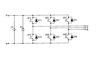
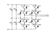
図1は第1の実施の形態の電力変換装置を示している。本実施の形態は、2レベル、3相回路で構成される電力変換装置であり、電力変換回路のUVW各相のブリッジの上アーム、下アームそれぞれをIGBT素子のような半導体スイッチング素子Q11〜Q32と、半導体スイッチング素子Q11〜Q32それぞれと逆並列に接続されたSiCのSBD又はJBSの還流ダイオードD11〜D32とによって構成し、電力変換回路の直流側のP極−N極間にコンデンサC1を接続すると共に、コンデンサC1より交流側のP極−N極間に逆並列にSiウエハーを使ったPiNダイオードD1を接続している。
[First Embodiment]
FIG. 1 shows a power conversion apparatus according to the first embodiment. The present embodiment is a power conversion device configured by a two-level, three-phase circuit, and the upper and lower arms of the UVW each phase bridge of the power conversion circuit are connected to semiconductor switching elements Q11 to Q32 such as IGBT elements. And a SBD of SiC or JBS freewheeling diodes D11 to D32 connected in antiparallel with each of the semiconductor switching elements Q11 to Q32, and a capacitor C1 is connected between the P pole and the N pole on the DC side of the power conversion circuit In addition, a PiN diode D1 using a Si wafer is connected in reverse parallel between the P pole and the N pole on the AC side of the capacitor C1.
本実施の形態の電力変換装置は、次のように動作する。通常、2レベル、3相回路で構成される電力変換装置では、図9に示すように、上側半導体スイッチング素子Q11と下側半導体スイッチング素子Q12が同時に導通状態になり、P極−N極間短絡が発生すると主回路インダクタンスL1,L2とコンデンサC1によって電圧、電流が振動的になり、点線で示すようなN極からP極へ流れる反転電流が発生する。この反転電流が健全素子の還流ダイオードD11,D12で分流される時に、SBD、JBSはPiNダイオードに比べてサージ電流耐量が弱いため、還流ダイオードD11,D12にPiNダイオードを使用した電力変換装置に比べ素子破壊の可能性が高い。 The power conversion device according to the present embodiment operates as follows. Normally, in a power conversion device constituted by a two-level, three-phase circuit, as shown in FIG. 9, the upper semiconductor switching element Q11 and the lower semiconductor switching element Q12 are in a conductive state at the same time, and the P pole-N pole short circuit Occurs, the main circuit inductances L1 and L2 and the capacitor C1 make the voltage and current oscillate, and an inversion current flowing from the N pole to the P pole as shown by the dotted line is generated. When this inversion current is shunted by the free-wheeling diodes D11 and D12, the SBD and JBS have a weaker surge current resistance than the PiN diode, and therefore, compared to a power converter using a PiN diode as the free-wheeling diodes D11 and D12. There is a high possibility of device destruction.
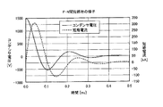
そこで、本実施の形態の電力変換装置では、コンデンサC1より交流側のP極−N極間に逆並列にPiNダイオードD1を接続することにより、P極−N極間短絡が発生し反転電流が流れるようになった場合、その反転電流を還流ダイオードD11〜D32に分流させると同時にPiNダイオードD1にも分流させる。そしてこの場合、SiCのSBDダイオードはPiNダイオードに比べて内部インピーダンスが大きい。例えば、図10のグラフでは100kAのサージ電流に対してSBDダイオードは定格電流の100倍以上となるので、サージ電流はSBDダイオードにはほとんど分流しないで、Si−PiNダイオードに分流することになる。したがって、本実施の形態によれば、サージ電流の多くを、PiNダイオードに分流することができ、還流ダイオードD11〜D32であるSBD、JBSダイオードの通電電流を低減し、SBD又はJBSの還流ダイオードが破壊し、IGBTモジュールの破壊が発生、拡大するのを抑制することができる。 Therefore, in the power conversion device of the present embodiment, by connecting the PiN diode D1 in reverse parallel between the P pole and the N pole on the AC side of the capacitor C1, a short circuit between the P pole and the N pole occurs, and the inversion current is generated. When the current flows, the inversion current is shunted to the freewheeling diodes D11 to D32 and simultaneously to the PiN diode D1. In this case, the SiC SBD diode has a larger internal impedance than the PiN diode. For example, in the graph of FIG. 10, since the SBD diode is 100 times or more the rated current with respect to a surge current of 100 kA, the surge current is hardly shunted to the SBD diode but is shunted to the Si-PiN diode. Therefore, according to the present embodiment, most of the surge current can be shunted to the PiN diode, the conduction current of the SBD and JBS diodes that are the freewheeling diodes D11 to D32 is reduced, and the freewheeling diode of the SBD or JBS It is possible to suppress the occurrence and expansion of the destruction of the IGBT module.
[第2の実施の形態]
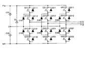
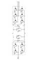
図2は第2の実施の形態の電力変換装置を示している。本実施の形態は、3レベル、3相回路で構成される電力変換装置であり、電力変換回路のUVW各相のブリッジの上アーム、下アームそれぞれをIGBT素子のような半導体スイッチング素子Q111〜Q322と、半導体スイッチング素子Q111〜Q322それぞれと逆並列に接続されたSiCのSBD又はJBSの還流ダイオードD111〜D322と、中点Cと上アームの素子接続点との間、中点Cと下アームの素子接続点との間それぞれに接続されたSiCのSBD又はJBSの還流ダイオードD101〜D302とによって構成し、P極−中点C間、中点C−N極間それぞれにコンデンサC2U,C2Dを接続すると共に、コンデンサC2U,C2Dより交流側のP極−N極間に逆並列にPiNダイオードD2を接続している。
[Second Embodiment]
FIG. 2 shows a power conversion apparatus according to the second embodiment. The present embodiment is a power conversion device configured by a three-level, three-phase circuit, and the upper and lower arms of the UVW each phase bridge of the power conversion circuit are connected to semiconductor switching elements Q111 to Q322 such as IGBT elements. And between the SBD of SiC SBD or JBS freewheel diodes D111 to D322 connected in antiparallel with the semiconductor switching elements Q111 to Q322, and between the middle point C and the upper arm element connection point, between the middle point C and the lower arm. Consists of SiC SBD or JBS free-wheeling diodes D101 to D302 connected between the element connection points, and capacitors C2U and C2D are connected between the P pole and the midpoint C and between the midpoint C and the N pole, respectively. In addition, a PiN diode D2 is connected in antiparallel between the P pole and the N pole on the AC side of the capacitors C2U and C2D.
3レベル、3相回路で構成される電力変換装置でも、P極−N極間短絡が発生すると主回路インダクタンスとコンデンサC2U,C2Dによって電圧、電流が振動的になり、N極からP極へ流れる反転電流が発生する。これに対して、本実施の形態の電力変換装置では、コンデンサC2U,C2Dより交流側のP極−N極間に逆並列にSiウエハーを使ったPiNダイオードD2を接続することにより、P極−N極間短絡が発生し反転電流が流れるようになった場合、その反転電流を還流ダイオードD111〜D322,D101〜D302に分流させると同時にPiNダイオードD2にも分流させることができ、還流ダイオードD111〜D322,D101〜D302であるSBD、JBSの通電電流を低減し、SBD又はJBSの還流ダイオードが破壊し、IGBTモジュールの破壊が発生、拡大するのを抑制することができる。 Even in a power conversion device constituted by a three-level, three-phase circuit, when a short circuit between the P pole and the N pole occurs, the voltage and current become oscillating due to the main circuit inductance and the capacitors C2U and C2D, and flows from the N pole to the P pole. An inversion current is generated. On the other hand, in the power conversion device of the present embodiment, by connecting a PiN diode D2 using a Si wafer in reverse parallel between the P pole and the N pole on the AC side of the capacitors C2U and C2D, the P pole− When a short circuit occurs between the N poles and an inversion current flows, the inversion current can be diverted to the free-wheeling diodes D111 to D322, D101 to D302 and simultaneously to the PiN diode D2, and the free-wheeling diode D111 to The energization current of SBD and JBS D322, D101 to D302 can be reduced, and the SBD or JBS free wheel diode can be prevented from being broken and the IGBT module from being broken or expanded.
[第3の実施の形態]
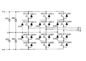
図3は第3の実施の形態の電力変換装置を示している。本実施の形態は、3レベル、3相回路で構成される電力変換装置であり、電力変換回路のUVW各相のブリッジの上アーム、下アームそれぞれをIGBT素子のような半導体スイッチング素子Q111〜Q322と、半導体スイッチング素子Q111〜Q322それぞれと逆並列に接続されたSiCのSBD又はJBSの還流ダイオードD111〜D322と、中点Cと上アームの素子接続点との間、中点Cと下アームの素子接続点との間それぞれに接続されたSiCのSBD又はJBSの還流ダイオードD101〜D302とによって構成し、P極−中点C間、中点C−N極間それぞれにコンデンサC2U,C2Dを接続すると共に、コンデンサC2U,C2Dより交流側のP極−中点C間、中点C−N極間それぞれに逆並列にSiウエハーを使ったPiNダイオードD2U,D2Dを接続している。
[Third Embodiment]
FIG. 3 shows a power conversion apparatus according to the third embodiment. The present embodiment is a power conversion device configured by a three-level, three-phase circuit, and the upper and lower arms of the UVW each phase bridge of the power conversion circuit are connected to semiconductor switching elements Q111 to Q322 such as IGBT elements. And between the SBD of SiC SBD or JBS freewheel diodes D111 to D322 connected in antiparallel with the semiconductor switching elements Q111 to Q322, and between the middle point C and the upper arm element connection point, between the middle point C and the lower arm. Consists of SiC SBD or JBS free-wheeling diodes D101 to D302 connected between the element connection points, and capacitors C2U and C2D are connected between the P pole and the midpoint C and between the midpoint C and the N pole, respectively. In addition, the Si wafer is connected in reverse parallel between the P pole and the midpoint C on the AC side of the capacitors C2U and C2D and between the midpoint C and N pole PiN diode D2U using, are connected to the D2D.
3レベル、3相回路で構成される電力変換装置でも、P極−N極間短絡が発生すると主回路インダクタンスとコンデンサC2U,C2Dによって電圧、電流が振動的になり、N極からP極へ流れる反転電流が発生する。これに対して、本実施の形態の電力変換装置では、コンデンサC2U,C2Dより交流側のP極−中点C間、中点C−N極間それぞれに逆並列にPiNダイオードD2U,D2Dを接続することにより、P極−N極間短絡が発生し反転電流が流れるようになった場合、その反転電流を還流ダイオードD111〜D322,D101〜D302に分流させると同時にPiNダイオードD2にも分流させることができ、還流ダイオードD111〜D322,D101〜D302であるSBD、JBSの通電電流を低減し、SBD又はJBSの還流ダイオードが破壊し、IGBTモジュールの破壊が発生、拡大するのを抑制することができる。 Even in a power conversion device constituted by a three-level, three-phase circuit, when a short circuit between the P pole and the N pole occurs, the voltage and current become oscillating due to the main circuit inductance and the capacitors C2U and C2D, and flows from the N pole to the P pole. An inversion current is generated. On the other hand, in the power converter of the present embodiment, PiN diodes D2U and D2D are connected in antiparallel between the P pole and the middle point C on the AC side of the capacitors C2U and C2D and between the middle point C and the N pole, respectively. By doing this, when a short circuit between the P pole and the N pole occurs and an inversion current flows, the inversion current is shunted to the free-wheeling diodes D111 to D322, D101 to D302 and simultaneously to the PiN diode D2. It is possible to reduce the energization current of the SBD and JBS which are the freewheeling diodes D111 to D322 and D101 to D302, and to prevent the freewheeling diode of the SBD or JBS from being broken and the IGBT module from being broken or expanded. .
加えて、3レベル、3相回路の電力変換装置では、P極−N極間だけでなく、P極−中点C間や中点C−N極間でも短絡が発生する。短絡電流は主回路インダクタンスとコンデンサC2U又はC2Dによって電圧、電流が振動的になり、中点CからP極、又はN極から中点Cへ流れる反転電流が発生するが、本実施の形態では、コンデンサC2U,C2Dより交流側のP極−中点C間、及び中点C−N極間に逆並列にPiNダイオードD2U,D2Dを接続することで、反転電流をPiNダイオードD2U,D2Dにも分流させて、還流ダイオードであるSBD、JBSの分流割合を低減し、素子破壊を抑制することができる。 In addition, in a three-level, three-phase circuit power converter, a short circuit occurs not only between the P pole and the N pole, but also between the P pole and the middle point C or between the middle point C and N poles. The short-circuit current is oscillated in voltage and current by the main circuit inductance and the capacitor C2U or C2D, and an inversion current flowing from the middle point C to the P pole or from the N pole to the middle point C is generated. By connecting PiN diodes D2U and D2D in reverse parallel between the P pole and the middle point C on the AC side of the capacitors C2U and C2D and between the middle point C and N poles, the inversion current is also shunted to the PiN diodes D2U and D2D. Thus, the shunt ratio of SBD and JBS, which are freewheeling diodes, can be reduced, and element breakdown can be suppressed.
[第4の実施の形態]
図4は第4の実施の形態の電力変換装置を示している。本実施の形態は、2レベル、単相回路で構成される電力変換装置であり、電力変換回路のUV各相のブリッジの上アーム、下アームそれぞれをIGBT素子のような半導体スイッチング素子Q11〜Q22と、半導体スイッチング素子Q11〜Q22それぞれと逆並列に接続されたSiCのSBD又はJBSの還流ダイオードD11〜D22とによって構成し、電力変換回路の直流側のP極−N極間にコンデンサC1を接続すると共に、コンデンサC1より交流側のP極−N極間に逆並列にSiウエハーを使ったPiNダイオードD1を接続している。
[Fourth Embodiment]
FIG. 4 shows a power conversion apparatus according to the fourth embodiment. The present embodiment is a power conversion device configured by a two-level, single-phase circuit, and the upper and lower arms of each UV bridge of the power conversion circuit are connected to semiconductor switching elements Q11 to Q22 such as IGBT elements. And a SBD of SiC or JBS freewheeling diodes D11 to D22 connected in antiparallel with each of the semiconductor switching elements Q11 to Q22, and a capacitor C1 is connected between the P pole and the N pole on the DC side of the power conversion circuit In addition, a PiN diode D1 using a Si wafer is connected in reverse parallel between the P pole and the N pole on the AC side of the capacitor C1.
本実施の形態の電力変換装置では、コンデンサC1より交流側のP極−N極間に逆並列にSiウエハーを使ったPiNダイオードD1を接続することにより、P極−N極間短絡が発生し反転電流が流れるようになった場合、その反転電流を還流ダイオードD11〜D22に分流させると同時にPiNダイオードD1にも分流させることができ、還流ダイオードD11〜D22であるSBD、JBSの通電電流を低減し、SBD又はJBSの還流ダイオードが破壊し、IGBTモジュールの破壊が発生、拡大するのを抑制することができる。 In the power converter according to the present embodiment, a PN-N pole short circuit occurs by connecting a PiN diode D1 using a Si wafer in antiparallel between the P pole-N pole on the AC side of the capacitor C1. When the inversion current starts to flow, the inversion current can be shunted to the freewheeling diodes D11 to D22 and simultaneously to the PiN diode D1 to reduce the energization current of the SBD and JBS that are the freewheeling diodes D11 to D22. In addition, it is possible to prevent the SBD or JBS reflux diode from being broken and the IGBT module from being broken and expanded.
[第5の実施の形態]
図5は第5の実施の形態の電力変換装置を示している。本実施の形態は、3レベル、単相回路で構成される電力変換装置であり、電力変換回路のUV各相のブリッジの上アーム、下アームそれぞれをIGBT素子のような半導体スイッチング素子Q111〜Q222と、半導体スイッチング素子Q111〜Q222それぞれと逆並列に接続されたSiCのSBD又はJBSの還流ダイオードD111〜D222と、中点Cと上アームの素子接続点との間、中点Cと下アームの素子接続点との間それぞれに接続されたSiCのSBD又はJBSの還流ダイオードD101〜D202とによって構成し、P極−中点C間、中点C−N極間それぞれにコンデンサC2U,C2Dを接続すると共に、コンデンサC2U,C2Dより交流側のP極−N極間に逆並列にSiウエハーを使ったPiNダイオードD2を接続している。
[Fifth Embodiment]
FIG. 5 shows a power conversion apparatus according to the fifth embodiment. The present embodiment is a power conversion device configured by a three-level, single-phase circuit, and each of the upper and lower arms of each UV bridge of the power conversion circuit includes semiconductor switching elements Q111 to Q222 such as IGBT elements. And between the SBD of SiC SBD or JBS freewheel diodes D111 to D222 connected in antiparallel with the semiconductor switching elements Q111 to Q222, the midpoint C and the upper arm element connection point, the midpoint C and the lower arm Consists of SiC SBD or JBS free-wheeling diodes D101 to D202 connected between the element connection points, and capacitors C2U and C2D are connected between the P pole and the middle point C and between the middle point C and the N pole, respectively. PiN diode D using Si wafer in antiparallel between P pole and N pole on the AC side of capacitors C2U and C2D It is connected to.
3レベル、単相回路で構成される電力変換装置でも、P極−N極間短絡が発生すると主回路インダクタンスとコンデンサC2U,C2Dによって電圧、電流が振動的になり、N極からP極へ流れる反転電流が発生する。これに対して、本実施の形態の電力変換装置では、コンデンサC2U,C2Dより交流側のP極−N極間に逆並列にPiNダイオードD2を接続することにより、P極−N極間短絡が発生し反転電流が流れるようになった場合、その反転電流を還流ダイオードD111〜D222,D101〜D202に分流させると同時にPiNダイオードD2にも分流させることができ、還流ダイオードD111〜D222,D101〜D202であるSBD、JBSの通電電流を低減し、SBD又はJBSの還流ダイオードが破壊し、IGBTモジュールの破壊が発生、拡大するのを抑制することができる。 Even in a power converter configured with a three-level, single-phase circuit, when a short circuit between the P pole and the N pole occurs, the voltage and current become oscillating due to the main circuit inductance and the capacitors C2U and C2D, and flows from the N pole to the P pole. An inversion current is generated. On the other hand, in the power converter of the present embodiment, the PN-N pole short circuit is caused by connecting the PiN diode D2 in antiparallel between the P-pole and N-pole on the AC side of the capacitors C2U and C2D. When the reverse current is generated and the reverse current flows, the reverse current can be shunted to the free-wheeling diodes D111 to D222, D101 to D202 and simultaneously to the PiN diode D2, so that the free-wheeling diodes D111 to D222, D101 to D202 It is possible to reduce the SBD and JBS energization currents, and to prevent the SBD or JBS reflux diode from being broken, and the IGBT module from being broken and expanded.
[第6の実施の形態]
図6は第6の実施の形態の電力変換装置を示している。本実施の形態は、3レベル、単相回路で構成される電力変換装置であり、電力変換回路のUV各相のブリッジの上アーム、下アームそれぞれをIGBT素子のような半導体スイッチング素子Q111〜Q222と、半導体スイッチング素子Q111〜Q222それぞれと逆並列に接続されたSiCのSBD又はJBSの還流ダイオードD111〜D222と、中点Cと上アームの素子接続点との間、中点Cと下アームの素子接続点との間それぞれに接続されたSiCのSBD又はJBSの還流ダイオードD101〜D202とによって構成し、P極−中点C間、中点C−N極間それぞれにコンデンサC2U,C2Dを接続すると共に、コンデンサC2U,C2Dより交流側のP極−中点C間、中点C−N極間それぞれに逆並列にSiウエハーを使ったPiNダイオードD2U,D2Dを接続している。
[Sixth Embodiment]
FIG. 6 shows a power conversion apparatus according to the sixth embodiment. The present embodiment is a power conversion device configured by a three-level, single-phase circuit, and each of the upper and lower arms of each UV bridge of the power conversion circuit includes semiconductor switching elements Q111 to Q222 such as IGBT elements. Between the SBD of SiC or JBS freewheeling diodes D111 to D222 connected in reverse parallel to the semiconductor switching elements Q111 to Q222, the midpoint C and the upper arm element connection point, the midpoint C and the lower arm Consists of SiC SBD or JBS free-wheeling diodes D101 to D202 connected between the element connection points, and capacitors C2U and C2D are connected between the P pole and the middle point C and between the middle point C and the N pole, respectively. In addition, the Si wafer is connected in reverse parallel between the P pole and the midpoint C on the AC side of the capacitors C2U and C2D and between the midpoint C and N pole PiN diode D2U using, connect the D2D.
3レベル、単相回路で構成される電力変換装置でも、P極−N極間短絡が発生すると主回路インダクタンスとコンデンサC2U,C2Dによって電圧、電流が振動的になり、N極からP極へ流れる反転電流が発生する。これに対して、本実施の形態の電力変換装置では、コンデンサC2U,C2Dより交流側のP極−中点C間、中点C−N極間それぞれに逆並列にPiNダイオードD2U,D2Dを接続することにより、P極−N極間短絡が発生し反転電流が流れるようになった場合、その反転電流を還流ダイオードD111〜D222,D101〜D202に分流させると同時にPiNダイオードD2U,D2Dにも分流させることができ、還流ダイオードD111〜D222,D101〜D202であるSBD、JBSの通電電流を低減し、SBD又はJBSの還流ダイオードが破壊し、IGBTモジュールの破壊が発生、拡大するのを抑制することができる。 Even in a power converter configured with a three-level, single-phase circuit, when a short circuit between the P pole and the N pole occurs, the voltage and current become oscillating due to the main circuit inductance and the capacitors C2U and C2D, and flows from the N pole to the P pole. An inversion current is generated. On the other hand, in the power converter of the present embodiment, PiN diodes D2U and D2D are connected in antiparallel between the P pole and the middle point C on the AC side of the capacitors C2U and C2D and between the middle point C and the N pole, respectively. Thus, if a short circuit between the P pole and the N pole occurs and an inversion current flows, the inversion current is shunted to the free-wheeling diodes D111 to D222 and D101 to D202, and at the same time to the PiN diodes D2U and D2D. The current flowing through the SBD and JBS, which are the freewheeling diodes D111 to D222 and D101 to D202, can be reduced, and the freewheeling diode of the SBD or JBS can be destroyed and the IGBT module can be prevented from being destroyed or expanded. Can do.
加えて、3レベル、単相回路の電力変換装置では、P極−N極間だけでなく、P極−中点C間や中点C−N極間でも短絡が発生する。短絡電流は主回路インダクタンスとコンデンサC2U又はC2Dによって電圧、電流が振動的になり、中点CからP極、又はN極から中点Cへ流れる反転電流が発生するが、本実施の形態では、コンデンサC2U,C2Dより交流側のP極−中点C間、及び中点C−N極間に逆並列にPiNダイオードD2U,D2Dを接続することで、反転電流をPiNダイオードD2U,D2Dにも分流させて、還流ダイオードであるSBD、JBSの分流割合を低減し、素子破壊を抑制することができる。 In addition, in a three-level, single-phase circuit power converter, a short circuit occurs not only between the P pole and the N pole, but also between the P pole and the middle point C and between the middle point C and N poles. The short-circuit current is oscillated in voltage and current by the main circuit inductance and the capacitor C2U or C2D, and an inversion current flowing from the middle point C to the P pole or from the N pole to the middle point C is generated. By connecting PiN diodes D2U and D2D in reverse parallel between the P pole and the middle point C on the AC side of the capacitors C2U and C2D and between the middle point C and N poles, the inversion current is also shunted to the PiN diodes D2U and D2D. Thus, the shunt ratio of SBD and JBS, which are freewheeling diodes, can be reduced, and element breakdown can be suppressed.
[第7の実施の形態]
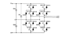
第1、第4の実施の形態それぞれでは、コンデンサC1とSiウエハーを使ったPiNダイオードD1をP極−N極間に並列に接続した。第3、第6の実施の形態それぞれでは、コンデンサC2UとSiウエハーを使ったPiNダイオードD2U、コンデンサC2DとSiウエハーを使ったPiNダイオードD2DをP極−中点C間、中点C−N極間それぞれに並列に接続した。
[Seventh Embodiment]
In each of the first and fourth embodiments, the capacitor C1 and the PiN diode D1 using the Si wafer are connected in parallel between the P pole and the N pole. In each of the third and sixth embodiments, the PiN diode D2U using the capacitor C2U and the Si wafer, and the PiN diode D2D using the capacitor C2D and the Si wafer are connected between the P pole and the midpoint C, and the midpoint CN pole. Each of them was connected in parallel.
本実施の形態は、図6に示すように、2レベル、単相回路の電力変換装置において、コンデンサC1の両端子に直接PiNダイオードD1を接続したことを特徴とする。尚、その他の回路要素については、図4の第4の実施の形態と共通する。 As shown in FIG. 6, this embodiment is characterized in that, in a power converter of a two-level, single-phase circuit, a PiN diode D1 is directly connected to both terminals of the capacitor C1. Other circuit elements are the same as those in the fourth embodiment shown in FIG.
このような構成の電力変換装置にあっても、第4の実施の形態と同様に、P極−N極間短絡が発生し反転電流が流れるようになった場合、その反転電流を還流ダイオードD11〜D22に分流させると同時にPiNダイオードD1にも分流させることができ、還流ダイオードD11〜D22であるSBD、JBSの通電電流を低減し、SBD又はJBSの還流ダイオードが破壊し、IGBTモジュールの破壊が発生、拡大するのを抑制することができる。 Even in the power conversion device having such a configuration, as in the case of the fourth embodiment, when a short circuit between the P pole and the N pole occurs and an inversion current flows, the inversion current is supplied to the freewheeling diode D11. Can be shunted to PiN diode D1 at the same time as shunting to D22, reducing the conduction current of SBD and JBS which are freewheeling diodes D11 to D22, the freewheeling diode of SBD or JBS being destroyed, and the IGBT module being destroyed Generation and expansion can be suppressed.
尚、図1に示した第1の実施の形態の2レベル、3相回路の電力変換装置に対しても、本実施の形態と同様に、そのコンデンサC1の端子に直接Siウエハーを使ったPiNダイオードD1を接続した構成とすることができる。 Note that the two-level, three-phase circuit power converter of the first embodiment shown in FIG. 1 also uses a PiN that uses a Si wafer directly at the terminal of the capacitor C1, as in the present embodiment. The diode D1 can be connected.
また、第3、第6の実施の形態それぞれに対しても、コンデンサC2Uの両端子に直接Siウエハーを使ったPiNダイオードD2Uを接続し、コンデンサC2Dの両端子に直接PiNダイオードD2Dを接続する構成とすることも可能である。 Also, in each of the third and sixth embodiments, the PiN diode D2U using a Si wafer is directly connected to both terminals of the capacitor C2U, and the PiN diode D2D is directly connected to both terminals of the capacitor C2D. It is also possible.
[第8の実施の形態]
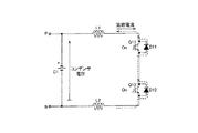
図8は、第8の実施の形態の電力変換装置の回路を示している。本実施の形態の電力変換装置は、単相交流−直流変換するコンバータ回路と、直流−3相交流変換するインバータ回路とを、それらの間にコンデンサC4,C1を介して接続した構成である。
[Eighth Embodiment]
FIG. 8 shows a circuit of the power conversion device according to the eighth embodiment. The power converter of this embodiment has a configuration in which a converter circuit that performs single-phase AC-DC conversion and an inverter circuit that performs DC-three-phase AC conversion are connected via capacitors C4 and C1 therebetween.
コンバータ回路は、上アーム、下アームそれぞれをIGBT素子のような半導体スイッチング素子Q61〜Q72と、半導体スイッチング素子Q61〜Q72それぞれと逆並列に接続されたSiCのSBD又はJBSの還流ダイオードD61〜D72とによって構成し、その直流側のP極−N極間にコンデンサC4を接続すると共に、コンデンサC4よりも交流側のP極−N極間に逆並列にSiウエハーを使ったPiNダイオードD5を接続している。さらに本実施の形態ではコンデンサC4の両端子に直接にSiウエハーを使ったPiNダイオードD4も接続している。 The converter circuit includes semiconductor switching elements Q61 to Q72 such as IGBT elements on the upper arm and the lower arm, and SiC SBD or JBS freewheeling diodes D61 to D72 connected in reverse parallel to the semiconductor switching elements Q61 to Q72, respectively. The capacitor C4 is connected between the P and N poles on the DC side, and the PiN diode D5 using a Si wafer is connected in reverse parallel between the P and N poles on the AC side of the capacitor C4. ing. Furthermore, in this embodiment, a PiN diode D4 using a Si wafer is directly connected to both terminals of the capacitor C4.
インバータ回路は、図1に示した第1の実施の形態と同様に、UVW各相のブリッジの上アーム、下アームそれぞれをIGBT素子のような半導体スイッチング素子Q11〜Q32と、半導体スイッチング素子Q11〜Q32それぞれと逆並列に接続されたSiCのSBD又はJBSの還流ダイオードD11〜D32とによって構成し、電力変換回路の直流側のP極−N極間にコンデンサC1を接続すると共に、コンデンサC1より交流側のP極−N極間に逆並列にSiウエハーを使ったPiNダイオードD3を接続している。さらに本実施の形態では、コンデンサC1の両端子に直接にSiウエハーを使ったPiNダイオードD1も接続している。 As in the first embodiment shown in FIG. 1, the inverter circuit includes semiconductor switching elements Q11 to Q32 such as IGBT elements each having an upper arm and a lower arm of the bridge of each UVW phase, and semiconductor switching elements Q11 to Q11. Q32 is composed of SiC SBD or JBS freewheeling diodes D11 to D32 connected in antiparallel to each of Q32, and a capacitor C1 is connected between the P pole and the N pole on the DC side of the power conversion circuit, and an AC is supplied from the capacitor C1. A PiN diode D3 using a Si wafer is connected in reverse parallel between the P pole and N pole on the side. Furthermore, in this embodiment, a PiN diode D1 using a Si wafer is directly connected to both terminals of the capacitor C1.
コンバータ、インバータで構成された電力変換装置でも、そのどちらかにP極−N極間短絡が発生し反転電流が流れるようになった場合、その反転電流を還流ダイオードに分流させると同時にPiNダイオードにも分流させることができ、還流ダイオードであるSBD、JBSの通電電流を低減し、SBD又はJBSの還流ダイオードが破壊し、IGBTモジュールの破壊が発生、拡大するのを抑制することができる。 Even in a power conversion device composed of a converter and an inverter, when a short circuit between the P pole and the N pole occurs in one of them and an inversion current flows, the inversion current is shunted to the free wheel diode and at the same time to the PiN diode. Therefore, it is possible to reduce the energization current of the SBD and JBS, which are the freewheeling diodes, to break down the freewheeling diodes of the SBD and JBS, and to suppress the occurrence and expansion of the IGBT module.
こうして、上記各実施の形態の還流ダイオードにSBD、JBSを使用した電力変換装置では、PiNダイオードを使用した電力変換装置に比べ、損失低減により装置の高効率化、小型化が図れると同時に、素子故障による信頼性の低下を抑制することができる。 Thus, in the power conversion device using SBD and JBS as the freewheeling diode in each of the above embodiments, the efficiency of the device can be improved and the size can be reduced by reducing the loss compared with the power conversion device using the PiN diode. A decrease in reliability due to a failure can be suppressed.
Q11〜Q32,Q111〜Q322 半導体スイッチング素子
D11〜D32,D111〜D322 還流ダイオード
D101〜D302 還流ダイオード
D1〜D5 PiNダイオード
C1,C2U,C2D コンデンサ
Q11 to Q32, Q111 to Q322 Semiconductor switching elements D11 to D32, D111 to D322 Free-wheeling diode D101 to D302 Free-wheeling diode D1 to D5 PiN diode C1, C2U, C2D Capacitor
Claims (8)
前記複数のスイッチング部の直流側であってP極とN極とに接続されたコンデンサと、
前記各スイッチング素子それぞれに逆並列に接続された複数のSiCを材料とする第1のダイオードと、
前記複数のスイッチング部に対して逆並列であって前記P極と前記N極とに接続され、
前記スイッチング部が短絡したときに発生する反転電流の一部を流すSiを材料とする第2のダイオードとを備えたことを特徴とする電力変換装置。 A plurality of switching units each of which corresponds to one of the phases of the power converter and includes at least one switching element belonging to the upper arm and at least one switching element belonging to the lower arm;
A capacitor on the DC side of the plurality of switching units and connected to the P and N poles;
A first diode made of a plurality of SiC materials connected in antiparallel to each of the switching elements;
Antiparallel to the plurality of switching units and connected to the P and N poles;
A power conversion device comprising: a second diode made of Si that allows a part of an inversion current generated when the switching unit is short-circuited.
前記複数のスイッチング部の直流側であって前記P極と前記中点とに接続された第1のコンデンサと、
前記複数のスイッチング部の直流側であって前記中点と前記N極とに接続された第2のコンデンサと、
前記各スイッチング素子それぞれに逆並列に接続された複数のSiCを材料とする第1のダイオードと、
前記複数のスイッチング部の上アームに属する各スイッチング素子に対して逆並列であって前記P極と前記中点とに接続されたSiを材料とする第2のダイオードと、
前記複数のスイッチング部の下アームに属する各スイッチング素子に対して逆並列であって前記中点と前記N極とに接続されたSiを材料とする第3のダイオードとを備え、
前記第2のダイオードと前記第3のダイオードは、前記スイッチング部が短絡したときに発生する反転電流の一部を流すことを特徴とする電力変換装置。 Each corresponds to one of the phases of the power converter, and is disposed between at least one switching element belonging to the upper arm disposed between the P pole and the midpoint and the midpoint and the N pole. A plurality of switching units comprising at least one switching element belonging to the lower arm;
A first capacitor connected to the P-pole and the midpoint on the DC side of the plurality of switching units;
A second capacitor on the DC side of the plurality of switching units and connected to the midpoint and the N pole;
A first diode made of a plurality of SiC materials connected in antiparallel to each of the switching elements;
A second diode made of Si that is antiparallel to each switching element belonging to the upper arms of the plurality of switching units and connected to the P-pole and the midpoint;
A third diode made of Si that is antiparallel to each switching element belonging to the lower arm of the plurality of switching units and connected to the midpoint and the N pole;
Said second diode and the third diode, to that power conversion apparatus characterized by flowing a part of the reverse current generated when the switching unit is short-circuited.
Priority Applications (4)
| Application Number | Priority Date | Filing Date | Title |
|---|---|---|---|
| JP2010141709A JP5611684B2 (en) | 2010-06-22 | 2010-06-22 | Power converter |
| US13/048,671 US8599585B2 (en) | 2010-06-22 | 2011-03-15 | Power conversion device |
| KR1020110060283A KR101281281B1 (en) | 2010-06-22 | 2011-06-21 | Power conversion device |
| CN201110178638.0A CN102299654B (en) | 2010-06-22 | 2011-06-22 | Power conversion device |
Applications Claiming Priority (1)
| Application Number | Priority Date | Filing Date | Title |
|---|---|---|---|
| JP2010141709A JP5611684B2 (en) | 2010-06-22 | 2010-06-22 | Power converter |
Publications (3)
| Publication Number | Publication Date |
|---|---|
| JP2012010427A JP2012010427A (en) | 2012-01-12 |
| JP2012010427A5 JP2012010427A5 (en) | 2013-11-14 |
| JP5611684B2 true JP5611684B2 (en) | 2014-10-22 |
Family
ID=45328526
Family Applications (1)
| Application Number | Title | Priority Date | Filing Date |
|---|---|---|---|
| JP2010141709A Active JP5611684B2 (en) | 2010-06-22 | 2010-06-22 | Power converter |
Country Status (4)
| Country | Link |
|---|---|
| US (1) | US8599585B2 (en) |
| JP (1) | JP5611684B2 (en) |
| KR (1) | KR101281281B1 (en) |
| CN (1) | CN102299654B (en) |
Families Citing this family (10)
| Publication number | Priority date | Publication date | Assignee | Title |
|---|---|---|---|---|
| JP5970194B2 (en) * | 2012-02-03 | 2016-08-17 | 株式会社 日立パワーデバイス | Semiconductor switching element drive circuit and power conversion circuit using the same |
| DE102013010188A1 (en) * | 2012-06-21 | 2013-12-24 | Fairchild Semiconductor Corp. | Switching circuit and control circuit |
| US9070571B2 (en) * | 2013-03-15 | 2015-06-30 | Infineon Technologies Ag | Power switching module with reduced oscillation |
| KR101636794B1 (en) * | 2013-08-12 | 2016-07-06 | 서울대학교산학협력단 | Current supperssion device of high voltage power transmission system and control method thereof |
| DE102014208139A1 (en) * | 2014-04-30 | 2015-11-05 | Robert Bosch Gmbh | Control device for an electric motor, vehicle and method |
| JP2017045901A (en) * | 2015-08-27 | 2017-03-02 | トヨタ自動車株式会社 | Freewheel diode and in-vehicle power supply |
| JP2018029412A (en) * | 2016-08-15 | 2018-02-22 | 株式会社東芝 | Power conversion device and power conversion system |
| DE102016216324A1 (en) * | 2016-08-30 | 2018-03-01 | Robert Bosch Gmbh | Drive system, in particular for a vehicle, and method for heating a drive system |
| JP7160007B2 (en) * | 2019-09-20 | 2022-10-25 | トヨタ自動車株式会社 | power supply |
| JP7835974B2 (en) * | 2021-12-13 | 2026-03-26 | ミネベアパワーデバイス株式会社 | Semiconductor devices and power converters |
Family Cites Families (13)
| Publication number | Priority date | Publication date | Assignee | Title |
|---|---|---|---|---|
| JPS645363A (en) * | 1987-06-25 | 1989-01-10 | Toshiba Corp | Inverter equipment |
| EP0838855B1 (en) * | 1991-09-20 | 2004-11-24 | Hitachi, Ltd. | Semiconductor module |
| JPH06276675A (en) | 1993-03-22 | 1994-09-30 | Nichicon Corp | Electrolytic capacitor bank |
| JP3396635B2 (en) * | 1998-10-23 | 2003-04-14 | 株式会社東芝 | Power converter |
| JP2002223573A (en) * | 2001-01-24 | 2002-08-09 | Toshiba Corp | 3-level power converter |
| US7820511B2 (en) * | 2004-07-08 | 2010-10-26 | Semisouth Laboratories, Inc. | Normally-off integrated JFET power switches in wide bandgap semiconductors and methods of making |
| DE102006010537B4 (en) | 2006-03-07 | 2009-06-10 | Siemens Ag | Diesel-electric drive system with a permanently excited synchronous generator |
| JP4772542B2 (en) | 2006-03-15 | 2011-09-14 | 株式会社東芝 | Power converter |
| JP2007305836A (en) | 2006-05-12 | 2007-11-22 | Mitsubishi Electric Corp | Power conversion circuit |
| JP2008017237A (en) | 2006-07-07 | 2008-01-24 | Mitsubishi Electric Corp | Electronic component and power converter using the electronic component |
| JP4240141B1 (en) * | 2007-10-09 | 2009-03-18 | ダイキン工業株式会社 | Direct AC power converter |
| JP2009159184A (en) | 2007-12-26 | 2009-07-16 | Hitachi Ltd | CIRCUIT DEVICE HAVING FREE WHEEL DIODE, CIRCUIT DEVICE USING DIODE AND POWER CONVERTER USING SAME |
| JP2010011555A (en) * | 2008-06-24 | 2010-01-14 | Origin Electric Co Ltd | Power conversion device |
-
2010
- 2010-06-22 JP JP2010141709A patent/JP5611684B2/en active Active
-
2011
- 2011-03-15 US US13/048,671 patent/US8599585B2/en not_active Expired - Fee Related
- 2011-06-21 KR KR1020110060283A patent/KR101281281B1/en not_active Expired - Fee Related
- 2011-06-22 CN CN201110178638.0A patent/CN102299654B/en not_active Expired - Fee Related
Also Published As
| Publication number | Publication date |
|---|---|
| CN102299654A (en) | 2011-12-28 |
| KR20110139148A (en) | 2011-12-28 |
| US20110310643A1 (en) | 2011-12-22 |
| US8599585B2 (en) | 2013-12-03 |
| CN102299654B (en) | 2014-05-28 |
| JP2012010427A (en) | 2012-01-12 |
| KR101281281B1 (en) | 2013-07-03 |
Similar Documents
| Publication | Publication Date | Title |
|---|---|---|
| JP5611684B2 (en) | Power converter | |
| Nami et al. | Five level cross connected cell for cascaded converters | |
| US8861235B2 (en) | Power converting apparatus | |
| CN102403914B (en) | Module switch, electricity inverter and the method for driving electricity inverter | |
| CN103069706B (en) | Indirect matrix converter | |
| JP5049964B2 (en) | Power converter | |
| US10411589B2 (en) | Power conversion apparatus and power semiconductor module | |
| US20160043659A1 (en) | Multilevel converter | |
| CN101978588A (en) | Power conversion device | |
| JP2016518809A (en) | Power conversion circuit and power conversion system | |
| JP2013146117A (en) | Multilevel power conversion circuit | |
| JP2015035902A (en) | Multi-level power converting device | |
| CN105119511B (en) | A kind of MMC submodular circuits with DC side failure blocking ability | |
| CN102957332B (en) | Three-level power conversion device | |
| CN115349220A (en) | Power converter | |
| JP6175946B2 (en) | Resonant inverter device | |
| CN107155387A (en) | Semiconductor device | |
| CN207638573U (en) | Modularized multi-level converter sub-module and modularization multi-level converter | |
| KR102261327B1 (en) | Inverter system | |
| JP2018029412A (en) | Power conversion device and power conversion system | |
| JP2011041348A (en) | Power converter | |
| CN110999054B (en) | Power module for converter and multilevel converter | |
| WO2017064848A1 (en) | Electric power conversion device and power conditioner using same | |
| CN108604877A (en) | The submodule of threaded link converter | |
| JP2019193459A (en) | Multi-level inverter |
Legal Events
| Date | Code | Title | Description |
|---|---|---|---|
| A621 | Written request for application examination |
Free format text: JAPANESE INTERMEDIATE CODE: A621 Effective date: 20130308 |
|
| A521 | Written amendment |
Free format text: JAPANESE INTERMEDIATE CODE: A523 Effective date: 20130926 |
|
| A977 | Report on retrieval |
Free format text: JAPANESE INTERMEDIATE CODE: A971007 Effective date: 20131114 |
|
| A131 | Notification of reasons for refusal |
Free format text: JAPANESE INTERMEDIATE CODE: A131 Effective date: 20131126 |
|
| A521 | Written amendment |
Free format text: JAPANESE INTERMEDIATE CODE: A523 Effective date: 20140124 |
|
| TRDD | Decision of grant or rejection written | ||
| A01 | Written decision to grant a patent or to grant a registration (utility model) |
Free format text: JAPANESE INTERMEDIATE CODE: A01 Effective date: 20140805 |
|
| A61 | First payment of annual fees (during grant procedure) |
Free format text: JAPANESE INTERMEDIATE CODE: A61 Effective date: 20140903 |
|
| R151 | Written notification of patent or utility model registration |
Ref document number: 5611684 Country of ref document: JP Free format text: JAPANESE INTERMEDIATE CODE: R151 |