JP5609068B2 - Spectrometer, image evaluation apparatus, and image forming apparatus - Google Patents
Spectrometer, image evaluation apparatus, and image forming apparatus Download PDFInfo
- Publication number
- JP5609068B2 JP5609068B2 JP2009253498A JP2009253498A JP5609068B2 JP 5609068 B2 JP5609068 B2 JP 5609068B2 JP 2009253498 A JP2009253498 A JP 2009253498A JP 2009253498 A JP2009253498 A JP 2009253498A JP 5609068 B2 JP5609068 B2 JP 5609068B2
- Authority
- JP
- Japan
- Prior art keywords
- light
- image
- diffraction element
- spectroscopic measurement
- incident
- Prior art date
- Legal status (The legal status is an assumption and is not a legal conclusion. Google has not performed a legal analysis and makes no representation as to the accuracy of the status listed.)
- Expired - Fee Related
Links
- 238000011156 evaluation Methods 0.000 title claims description 26
- 238000005259 measurement Methods 0.000 claims description 59
- 230000003595 spectral effect Effects 0.000 claims description 53
- 230000003287 optical effect Effects 0.000 claims description 44
- 238000003384 imaging method Methods 0.000 claims description 40
- 230000001678 irradiating effect Effects 0.000 claims description 7
- 238000012545 processing Methods 0.000 claims description 7
- 230000008859 change Effects 0.000 claims description 5
- 239000003086 colorant Substances 0.000 claims description 4
- 230000000737 periodic effect Effects 0.000 claims description 4
- 238000000034 method Methods 0.000 description 24
- 238000010586 diagram Methods 0.000 description 18
- 239000011159 matrix material Substances 0.000 description 12
- 238000005286 illumination Methods 0.000 description 11
- 238000009826 distribution Methods 0.000 description 10
- 239000000463 material Substances 0.000 description 7
- 238000012360 testing method Methods 0.000 description 7
- 238000012546 transfer Methods 0.000 description 5
- 238000001514 detection method Methods 0.000 description 4
- 238000004458 analytical method Methods 0.000 description 3
- 230000015572 biosynthetic process Effects 0.000 description 3
- 238000006243 chemical reaction Methods 0.000 description 3
- 238000005516 engineering process Methods 0.000 description 3
- 238000004088 simulation Methods 0.000 description 3
- 238000012935 Averaging Methods 0.000 description 2
- 238000012790 confirmation Methods 0.000 description 2
- 239000006185 dispersion Substances 0.000 description 2
- 230000014509 gene expression Effects 0.000 description 2
- 238000007689 inspection Methods 0.000 description 2
- 230000007246 mechanism Effects 0.000 description 2
- 229910044991 metal oxide Inorganic materials 0.000 description 2
- 150000004706 metal oxides Chemical class 0.000 description 2
- 239000004065 semiconductor Substances 0.000 description 2
- 239000000758 substrate Substances 0.000 description 2
- 230000009466 transformation Effects 0.000 description 2
- OKTJSMMVPCPJKN-UHFFFAOYSA-N Carbon Chemical compound [C] OKTJSMMVPCPJKN-UHFFFAOYSA-N 0.000 description 1
- VYZAMTAEIAYCRO-UHFFFAOYSA-N Chromium Chemical compound [Cr] VYZAMTAEIAYCRO-UHFFFAOYSA-N 0.000 description 1
- 238000004364 calculation method Methods 0.000 description 1
- 229910052799 carbon Inorganic materials 0.000 description 1
- 229910052804 chromium Inorganic materials 0.000 description 1
- 239000011651 chromium Substances 0.000 description 1
- 230000000295 complement effect Effects 0.000 description 1
- 230000007423 decrease Effects 0.000 description 1
- 230000001419 dependent effect Effects 0.000 description 1
- 238000006073 displacement reaction Methods 0.000 description 1
- 230000000694 effects Effects 0.000 description 1
- 239000011521 glass Substances 0.000 description 1
- 238000004519 manufacturing process Methods 0.000 description 1
- 239000012528 membrane Substances 0.000 description 1
- 229910052751 metal Inorganic materials 0.000 description 1
- 239000002184 metal Substances 0.000 description 1
- 239000000203 mixture Substances 0.000 description 1
- 230000009467 reduction Effects 0.000 description 1
- 239000011347 resin Substances 0.000 description 1
- 229920005989 resin Polymers 0.000 description 1
- 238000004611 spectroscopical analysis Methods 0.000 description 1
- 238000001228 spectrum Methods 0.000 description 1
- 238000006467 substitution reaction Methods 0.000 description 1
- 230000007704 transition Effects 0.000 description 1
- 230000007723 transport mechanism Effects 0.000 description 1
- 230000017105 transposition Effects 0.000 description 1
Images


Classifications
-
- G—PHYSICS
- G01—MEASURING; TESTING
- G01J—MEASUREMENT OF INTENSITY, VELOCITY, SPECTRAL CONTENT, POLARISATION, PHASE OR PULSE CHARACTERISTICS OF INFRARED, VISIBLE OR ULTRAVIOLET LIGHT; COLORIMETRY; RADIATION PYROMETRY
- G01J3/00—Spectrometry; Spectrophotometry; Monochromators; Measuring colours
- G01J3/12—Generating the spectrum; Monochromators
- G01J3/18—Generating the spectrum; Monochromators using diffraction elements, e.g. grating
-
- G—PHYSICS
- G01—MEASURING; TESTING
- G01J—MEASUREMENT OF INTENSITY, VELOCITY, SPECTRAL CONTENT, POLARISATION, PHASE OR PULSE CHARACTERISTICS OF INFRARED, VISIBLE OR ULTRAVIOLET LIGHT; COLORIMETRY; RADIATION PYROMETRY
- G01J3/00—Spectrometry; Spectrophotometry; Monochromators; Measuring colours
- G01J3/02—Details
- G01J3/0205—Optical elements not provided otherwise, e.g. optical manifolds, diffusers, windows
- G01J3/0229—Optical elements not provided otherwise, e.g. optical manifolds, diffusers, windows using masks, aperture plates, spatial light modulators or spatial filters, e.g. reflective filters
-
- G—PHYSICS
- G01—MEASURING; TESTING
- G01J—MEASUREMENT OF INTENSITY, VELOCITY, SPECTRAL CONTENT, POLARISATION, PHASE OR PULSE CHARACTERISTICS OF INFRARED, VISIBLE OR ULTRAVIOLET LIGHT; COLORIMETRY; RADIATION PYROMETRY
- G01J3/00—Spectrometry; Spectrophotometry; Monochromators; Measuring colours
- G01J3/02—Details
- G01J3/0294—Multi-channel spectroscopy
-
- G—PHYSICS
- G01—MEASURING; TESTING
- G01J—MEASUREMENT OF INTENSITY, VELOCITY, SPECTRAL CONTENT, POLARISATION, PHASE OR PULSE CHARACTERISTICS OF INFRARED, VISIBLE OR ULTRAVIOLET LIGHT; COLORIMETRY; RADIATION PYROMETRY
- G01J3/00—Spectrometry; Spectrophotometry; Monochromators; Measuring colours
- G01J3/12—Generating the spectrum; Monochromators
- G01J3/14—Generating the spectrum; Monochromators using refracting elements, e.g. prisms
-
- G—PHYSICS
- G01—MEASURING; TESTING
- G01J—MEASUREMENT OF INTENSITY, VELOCITY, SPECTRAL CONTENT, POLARISATION, PHASE OR PULSE CHARACTERISTICS OF INFRARED, VISIBLE OR ULTRAVIOLET LIGHT; COLORIMETRY; RADIATION PYROMETRY
- G01J3/00—Spectrometry; Spectrophotometry; Monochromators; Measuring colours
- G01J3/28—Investigating the spectrum
- G01J3/2803—Investigating the spectrum using photoelectric array detector
Description
本発明は、分光測定装置、画像評価装置及び画像形成装置に関する。 The present invention relates to a spectroscopic measurement apparatus, an image evaluation apparatus, and an image forming apparatus.
近年、プロダクションプリンティング分野において枚葉機、連帳機ともにデジタル化が進み、電子写真方式、インクジェット方式等による製品が数多く登場している。ユーザーニーズにおいても、モノクロ印刷からカラー印刷への移行における画像の多次元化、高精細高密度化が進み、写真高画質プリント、カタログ印刷、請求書等への個人嗜好に対応した広告掲載等、消費者の手元に届くサービス形態の多様化が進み、高画質、個人情報の確認、色再現への要求も高まっている。 In recent years, in the field of production printing, both sheet-fed machines and continuous book machines have been digitized, and many products using an electrophotographic system, an inkjet system, etc. have appeared. As for user needs, multi-dimensional images and high-definition and high-density images in the transition from monochrome printing to color printing have progressed, and high-quality photo prints, catalog printing, and advertisement placement corresponding to personal preferences for invoices, etc. With the diversification of service forms reaching consumers, demands for high image quality, confirmation of personal information, and color reproduction are also increasing.
画像形成装置において、高画質化に対応した技術として、電子写真方式では中間転写体や感光体上の定着前のトナー濃度を検知する濃度センサを搭載しトナー供給量を安定化するもの、個人情報の確認では、画像形成方式によらず出力画面をカメラ等で撮像し、文字認識や画像間差分による差異検出で検査するもの、色再現ではカラーパッチを出力して分光計に一点又は複数点の色計測を実行しキャリブレーションを行うもの等が上市されている。 In the image forming apparatus, as a technology that supports high image quality, the electrophotographic system is equipped with a density sensor that detects the toner density before fixing on the intermediate transfer member or the photosensitive member to stabilize the toner supply amount, personal information In the confirmation, the output screen is imaged by a camera or the like regardless of the image forming method, and inspection is performed by character recognition or difference detection based on the difference between images. In color reproduction, a color patch is output and one or more points are output to the spectrometer. Products that perform color measurement and perform calibration are on the market.
これらの技術は、ページ間、ページ内における画像変動に対応するため、画像全域で実行されることが望ましい。 These techniques are preferably executed over the entire image in order to cope with image variations between pages and within pages.
このように、画像の全幅計測における評価技術としては、特許文献1から5に記載されている方法が提案されている。 As described above, methods described in Patent Documents 1 to 5 have been proposed as evaluation techniques for measuring the full width of an image.
特許文献1には、ライン状の受光素子を複数並べて、測定対象を検出系に対して相対的に移動する機構を設定し、全幅の分光特性を計測する。その際、受光素子間で検出対象領域からの反射光クロストークが生じないように遮光壁を設定する技術が開示されている。 In Patent Document 1, a plurality of line-shaped light receiving elements are arranged, a mechanism for moving a measurement object relative to a detection system is set, and spectral characteristics of the full width are measured. In this case, a technique for setting a light shielding wall so that reflected light crosstalk from a detection target region does not occur between light receiving elements is disclosed.
また、特許文献2には、画像の全幅で異なる波長帯を有する光源で連続的に照射し、反射光を取得して全幅における分光特性を取得する技術が開示されている。 Japanese Patent Application Laid-Open No. 2004-228561 discloses a technique for continuously irradiating with light sources having different wavelength bands over the entire width of an image, acquiring reflected light, and acquiring spectral characteristics over the entire width.
また、特許文献3には、印刷面全幅に光を照射し、ラインセンサカメラにより、特定領域における濃度を検出し、平均化することにより、基準濃度を比較する技術が開示されている。 Patent Document 3 discloses a technique for comparing reference densities by irradiating light on the entire width of a printing surface, detecting density in a specific area with a line sensor camera, and averaging the detected density.
また、特許文献4には、原稿と特定原稿とを複数回走査し、共通する色味情報を画像間論理和等の処理から類似度を判定する技術が開示されている。 Patent Document 4 discloses a technique for scanning a manuscript and a specific manuscript a plurality of times, and determining the degree of similarity of common color information from processing such as inter-image OR.
また、特許文献5には、印刷面全幅に光を照射し、2次元の画素構造を持つCCD(Charge Coupled Device)と回折素子または屈折素子の組み合わせにより、全幅の分光特性を取得する技術が開示されている。
このように、画像の色を全幅で計測しようとした場合、異なる波長帯に限定した複数の光を照射して、エリアセンサにより撮像するか、ラインセンサで撮像しながら計測系と被検対象とを相対的に移動する構成、または、撮像系を複数設定し、撮像系に入射する被検対象からの反射光の波長帯を限定する構成が一般的に考えられる。その際、取得される複数の波長帯に対応した画像において、画像間で被検対象とする位置にずれが生じた場合、被検対象の各位置での色情報を正確に計測することが不可能となる。ここで波長帯の異なる複数の画像から色情報を正確に計測する方法として、各画像の被検対象の位置で取得される反射光量の強度をリファレンスとなる現画像や原稿データと比較する方法や、各画像の被検対象の位置で取得される反射光量の強度からウィナー推定等を適用して連続分布特性を推測する方法等がある。そのため、各画像で異なる位置を被検対象とした場合、リファレンスとの比較や、連続分光特性の推定に誤差が生じることとなり、測定精度が低下する原因となる。 In this way, when trying to measure the color of an image at its full width, it is possible to irradiate a plurality of light limited to different wavelength bands and take an image with an area sensor, or while taking an image with a line sensor. Generally, a configuration in which the wavelength of the reflected light from the subject to be examined that is set in a plurality of imaging systems and enters the imaging system is limited can be considered. At that time, in the images corresponding to a plurality of acquired wavelength bands, if there is a shift in the position to be tested between the images, it is impossible to accurately measure the color information at each position of the test target. It becomes possible. Here, as a method of accurately measuring color information from a plurality of images in different wavelength bands, a method of comparing the intensity of the reflected light amount acquired at the position of the subject of each image with a reference current image or document data, There is a method of estimating continuous distribution characteristics by applying Wiener estimation or the like from the intensity of the amount of reflected light acquired at the position of the subject to be examined in each image. For this reason, when a different position in each image is set as an object to be examined, an error occurs in comparison with a reference or estimation of continuous spectral characteristics, which causes a reduction in measurement accuracy.
ところで、引用文献1に記載されている技術では、ライン状の計測系であり、被検対象の画像の色を全幅で計測できる一般的な構成であるが、各波長帯で得られる画像の位置ズレを低減するものではない。 By the way, in the technique described in the cited document 1, it is a line-shaped measurement system and is a general configuration capable of measuring the color of the image to be examined in full width, but the position of the image obtained in each wavelength band. It does not reduce the deviation.
また、引用文献2に記載されている技術では、異なる波長帯を有する光源からの連続的な照射光による被検対象からの反射光を取得する構成では、時間軸におけるズレが生じ、被検対象の同一箇所を計測することはできない。仮に、このような構成で光源と受光系の組み合わせを複数備えたとしても、波長帯の異なる各画像の被検対象位置がずれる可能性が高くなる。また、異なる色でフィルター処理された複数列の検出器を用いた構成も記載されているが、この場合においても、複数色間での画像位置ずれによる問題が生じることは否めない。 Moreover, in the technique described in the cited document 2, in the configuration in which the reflected light from the test object by continuous irradiation light from light sources having different wavelength bands is acquired, a time-axis shift occurs, and the test object The same part of cannot be measured. Even if a plurality of combinations of light sources and light receiving systems are provided in such a configuration, there is a high possibility that the positions to be examined of the images having different wavelength bands are shifted. Also, a configuration using a plurality of rows of detectors filtered with different colors is described, but in this case as well, there is a problem that a problem due to image positional deviation between the plurality of colors occurs.
また、特許文献3に記載されている技術では、検知した領域の濃度を平均化することにより代表値を得ているものと推認されるが、被検対象の分布に関しては保証できる値を得ることができない。 Moreover, in the technique described in Patent Document 3, it is estimated that the representative value is obtained by averaging the density of the detected region, but a value that can be guaranteed is obtained for the distribution of the test object. I can't.
また、特許文献4に記載されている技術では、各波長帯に原稿と被検対象を画像間演算により比較して判定する方法であるが、この方法では、被検対象の色変動を特定することはできない。また、個別に得られる画像の色情報から、画像を再構成した場合においても、実際の被検対象に色変動が生じているか否かは判定することができない。 Further, the technique described in Patent Document 4 is a method of determining a document and a test object in each wavelength band by comparing them by calculation between images. In this method, the color variation of the test object is specified. It is not possible. Further, even when the image is reconstructed from the color information of the image obtained individually, it cannot be determined whether or not the color variation has occurred in the actual test object.
また、特許文献5に記載されている技術は、2次元画素構造を有するCCDを用い、一方向には画像データを、他の一方向には分光データを取得することで、全幅の色情報を特定する構成のものである。しかしながら、2次元画素構造を有するCCDにおいては、データ読出し特性の制約より、ラインセンサに対して、読出し速度が格段に遅くなるため、対象物の色情報を取得するためには、多大な時間を要するという問題点を有している。
Further, the technique described in
以上のように、従来の技術では、対象物の分光情報を全幅で計測する分光センサにおいては、高速に読出しを行うことと、分光精度を維持することを両立することは困難であった。 As described above, in the conventional technology, it is difficult to achieve both reading at high speed and maintaining spectral accuracy in a spectroscopic sensor that measures the spectral information of an object in full width.
本発明は、上記従来の技術に鑑みてなされたものであり、読取り対象物の分光特性を全幅で計測する際に、高速なデータ読出しができ、複数の波長帯における観測位置の位置合せが不要な分光測定装置、画像評価装置及び画像形成装置を提供することを目的とするものである。 The present invention has been made in view of the above-described conventional technology. When measuring the spectral characteristics of an object to be read in full width, high-speed data reading is possible, and alignment of observation positions in a plurality of wavelength bands is unnecessary. An object of the present invention is to provide a spectroscopic measurement apparatus, an image evaluation apparatus, and an image forming apparatus.
本発明は、画像担持媒体に光を照射する光照射部と、前記光照射部から画像担持媒体に照射された光の反射光を通過する複数の開口部を含むホールアレイと、前記ホールアレイを通過した光を結像する結像光学系と、前記結像光学系で結像された光を回折する回折素子と、前記回折素子により回折された光を複数の画素を含む分光センサ部で各々受光する受光部と、を有し、前記回折素子における回折格子の配列方向は、各々の前記開口部を通過した光が、各々前記分光センサ部における画素に入射するように、回折格子における構造が、前記結像光学系で結像された光が回折素子へ入射する角度に対応して、変化するように形成されていることを特徴とする。 The present invention relates to a light irradiating unit that irradiates light onto an image bearing medium, a hole array that includes a plurality of openings that pass reflected light of the light irradiated from the light irradiating unit onto the image bearing medium, and the hole array. An imaging optical system that forms an image of the light that has passed through, a diffraction element that diffracts the light imaged by the imaging optical system, and a spectral sensor unit that includes the light diffracted by the diffraction element, each including a plurality of pixels A light receiving portion for receiving light, and the arrangement direction of the diffraction grating in the diffraction element is such that the structure of the diffraction grating is such that light that has passed through each opening is incident on a pixel in the spectroscopic sensor portion. The light imaged by the imaging optical system is formed so as to change in accordance with the angle at which the light enters the diffraction element.
また、本発明は、前記回折素子は、表面に鋸波形状、階段形状の構造を周期的に形成されているもの、屈折率の異なる2種類の部材を張合わせた界面に、鋸波形状、階段形状の構造が周期的に形成されているもの、または、屈折率の変化している構造が周期的に形成されているものであって、前記受光部は、所定の数の画素ごとに複数の分光センサ部が形成されており、前記回折素子における前記周期は、前記複数の開口部を通過した光が、各々前記分光センサ部に入射するように形成されていることを特徴とする。 Further, in the present invention, the diffraction element has a sawtooth shape and a stepped structure periodically formed on the surface, and has a sawtooth shape on an interface between two members having different refractive indexes. A step-shaped structure is periodically formed, or a structure having a changed refractive index is periodically formed, and a plurality of the light receiving portions are provided for each predetermined number of pixels. spectroscopic and sensor portion is formed, the period of the diffraction element, the light passing through the plurality of openings, characterized in that it is made form such that each is morphism entering the spectroscopic sensor unit .
また、本発明は、前記回折素子は、表面に鋸波形状、階段形状の構造を周期的に形成されているもの、または、屈折率の異なる2種類の部材を張合わせた界面に、鋸波形状、階段形状の構造が周期的に形成されているものであって、前記受光部は、所定の数の画素ごとに複数の分光センサ部が形成されており、前記鋸波形状又は階段形状の構造の部分における高さは、前記複数の開口部を通過した光が、各々前記分光センサ部に入射するように形成されていることを特徴とする。 Further, according to the present invention, the diffraction element has a sawtooth or staircase structure periodically formed on the surface, or a sawtooth wave at an interface between two members having different refractive indexes. A structure having a shape and a staircase shape is periodically formed, and the light receiving portion has a plurality of spectral sensor portions for each predetermined number of pixels, and has a sawtooth shape or a staircase shape. height at portions of the structure, the light passing through the plurality of openings, characterized in that it is made form such that each enters the spectroscopic sensor unit.
また、本発明は、前記回折素子における回折格子の配列方向と、前記受光部における複数の画素の配列方向とが、平行ではないことを特徴とする。 Further, the invention is characterized in that the arrangement direction of the diffraction grating in the diffraction element and the arrangement direction of the plurality of pixels in the light receiving unit are not parallel.
また、本発明は、前記受光部に入射する光は、前記回折素子により回折された+1次回折光であることを特徴とする。 Further, the invention is characterized in that the light incident on the light receiving portion is + 1st order diffracted light diffracted by the diffraction element.
また、本発明は、前記所定の数は6以上であることを特徴とする。 Further, the present invention is characterized in that the predetermined number is 6 or more.
また、本発明は、画像担持媒体上に複数色で形成された画像の色彩を評価する画像評価装置において、前記記載の分光測定装置と、前記分光測定装置により得られた分光特性に基づき、前記画像における画像評価を行う処理部と、を有することを特徴とする。 Further, the present invention provides an image evaluation apparatus for evaluating the color of an image formed in a plurality of colors on an image bearing medium, based on the spectroscopic measurement apparatus described above and the spectral characteristics obtained by the spectroscopic measurement apparatus. And a processing unit that performs image evaluation on an image.
また、本発明は、前記記載の画像評価装置と、前記画像担持媒体に画像を形成する画像形成部と、を有することを特徴とする。 In addition, the present invention includes the above-described image evaluation apparatus and an image forming unit that forms an image on the image bearing medium.
本発明によれば、読取り対象物の分光特性を全幅で計測する際に、高速なデータ読出しができ、複数の波長帯における観測位置の位置合せが不要な分光測定装置、画像評価装置及び画像形成装置を提供することができる。 According to the present invention, when measuring the spectral characteristics of an object to be read in full width, it is possible to read data at high speed, and it is not necessary to align observation positions in a plurality of wavelength bands, an image evaluation apparatus, and image formation An apparatus can be provided.
本発明を実施するための形態について、以下に説明する。 The form for implementing this invention is demonstrated below.
〔第1の実施の形態〕
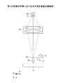
第1の実施の形態について説明する。本実施の形態における分光測定装置を図1及び図2に示す。図1は本実施の形態における分光測定装置の上面図であり、図2は本実施の形態における分光測定装置の側面図である。尚、本実施の形態における分光測定装置を説明する際には、X方向、Y方向、Z方向との表現を用いる場合があるが、これらはいずれも図中に記載されているX軸方向、Y軸方向、Z軸方向を示すものである。
[First Embodiment]
A first embodiment will be described. The spectroscopic measurement apparatus in this embodiment is shown in FIGS. FIG. 1 is a top view of the spectrometer in the present embodiment, and FIG. 2 is a side view of the spectrometer in the present embodiment. In the description of the spectroscopic measurement apparatus in the present embodiment, expressions such as the X direction, the Y direction, and the Z direction may be used. It shows the Y-axis direction and the Z-axis direction.
本実施の形態における分光測定装置は、ライン照明光源12、レンズ13、セルフォックレンズ14、ホールアレイ15、結像光学系16、回折素子17、ラインセンサ18等を有している。尚、破線は、画像担持媒体11からの拡散反射光の光路を示すものである。
The spectroscopic measurement apparatus in the present embodiment includes a line
ライン照明光源12は、例えば、可視光のほぼ全域において所定の強度を有する白色のLED(Light Emitting Diode:発光ダイオード)アレイを用いることができる。尚、ライン照明光源12としては、この他、冷陰極管等の蛍光灯やランプ光源等を用いることも可能である。ライン照明光源12としては、分光に必要な広い波長領域の光を発することができるものであって、画像担持媒体11を均一に照明することができるものであることが好ましい。
As the line
レンズ13は、ライン照明光源12から出射された光を紙等からなる画像担持媒体11にコリメートして(平行光として)、または、集光して照射する機能を有するものである。これにより紙等からなる画像担持媒体11には、ライン光源12から発せられた光が画像担持媒体11の奥行き方向に広がりのあるライン状に照明される。尚、本実施の形態では、ライン照明光源12及びレンズ13を用いた構成を示すが、レンズ13を省略した構成とすることも可能である。
The
セルフォックレンズ14は、画像担持媒体11に形成されている画像を後述するホールアレイ15上に結像する機能を有するものである。正し、必ずしも正確にホールアレイ15上に結像している必要はなく、ホールアレイ15上においてデフォーカスした状態であってもよい。尚、本実施の形態では、セルフォックレンズ14を用いた構成を示すが、セルフォックレンズ14に代えて、マイクロレンズアレイやその他の等倍結像光学素子、複数のレンズからなる結像レンズを用いることも可能である。
The
ホールアレイ15は、後述するように、複数の開口部が一列に配列されているものである。ホールアレイ15を透過した光は、結像光学系16及び回折素子17により分光された後、ラインセンサ18の画像検出のための画素上にホールアレイ15上における像として結像される。
As will be described later, the
結像光学系16は、一般的なスキャナー光学系に用いられるレンズや、工業的に用いられているラインセンサ用レンズを用いることが可能である。例えば、ラインセンサ用レンズとしては、ML−L02035(モリテックス社)が挙げられ、このラインセンサ用レンズにおいては、0.2倍の倍率で、X軸方向に約300mmの画像をX軸方向に約60mmの像としてラインセンサ18上に結像させることができる。尚、本願において結像光学系16によって結像される像の像高とは、結像光学系16によってラインセンサ18上に結像される像において、結像光学系16の光軸中心を原点としたときのX軸方向における位置、即ち、ラインセンサ18における画素21の配列方向における位置を意味するものである。
The imaging
ラインセンサ18は、複数のライン状に配列された画素により構成されており、回折素子17を介して入射する所定の波長帯の拡散反射光量を取得するための受光素子としての機能を有している。ラインセンサ18としては、例えば、MOS(Metal Oxide Semiconductor Device)、CMOS(Complimentary Metal Oxide Semiconductor Device)、CCD(Charge Coupled Device)、CIS(Contact Image Sensor)、PDA(Photo Diode Array)等を用いることができる。本実施の形態では、ラインセンサ18として、画素数が8192画素であって、画素ピッチpが7μmで形成されたCCDラインセンサを用いた。
The
次に、ラインセンサ18について説明する。図3は、ラインセンサ18の画素構造を模式的に示す構造図である。図示されるように、ラインセンサ18は、X方向に一列に複数21の画素が配列されたものである。ラインセンサ18は、X方向に配列されたN個の画素21を一群とする複数の分光センサ部22を有している。各々の分光センサ部22におけるN個の画素21は、互いに分光特性の異なる光を受光するものである。尚、図3においては、一例として、N=6の場合のラインセンサ18を示している。
Next, the
具体的には、図4に示すように、回折素子17は、ラインセンサ18から距離t離れた位置に近接して配置されており、破線で示される光路のように、ラインセンサ18において、入射光をX方向に回折させることにより、分光センサ部22におけるN個の画素21に異なる分光特性の光を入射させることができるよう構成されている。図示されるように、本実施の形態における回折素子17は、透明基板の表面に断面形状が鋸歯形状のものを周期的に形成したものである。本実施の形態における回折素子17は、回折素子17の鋸歯形状の回折格子の配列方向、即ち、矢印Bに示す回折格子ベクトルの方向が、X方向と一致している。また、回折素子17の鋸歯形状は周期dで形成されており、数1に示されるように、波長λの光が回折素子17に角度θinで入射した場合、角度θmに回折する。尚、mは、回折素子17における回折次数であり整数である。尚、回折素子17の鋸歯形状は高さhで形成されている。
Specifically, as shown in FIG. 4, the

数1に示す式より、波長λに依存して角度θmは変化するため、所定の波長帯の光を分光センサ部22におけるN個の画素21のうち、所定の画素21に入射させることができる。
Since the angle θ m changes depending on the wavelength λ, the light in the predetermined wavelength band can be incident on the
また、図4に示す回折素子17では、回折素子17の形状を鋸歯形状とすることにより、+1次の回折光(数1における式においてm=1となる光)の強度を強くすることができ好ましい。よって、本実施の形態における回折素子17としては、+1次の回折光が主となる回折素子を用いる。
Further, in the
回折素子17としては、上述した鋸歯形状の回折素子の他、図5に示すように、表面に階段状の形状が形成されたものでもよく、また、図6に示すように、2つの異なる屈折率の材料を張合わせたものであって、2つの異なる屈折率の材料が接する界面を鋸波形状に形成したものであってもよい。具体的には、図6に示す回折素子は、第1の回折素子部材23を低屈折率高分散材料により形成し、第2の回折素子部材24を高屈折率低分散材料により形成し、第1の回折素子部材23と第2の回折素子部材24との界面は、断面形状が周期dの鋸歯形状に形成されているものである。これにより、より広い波長範囲において高い回折効率を得ることが可能となる。
As the
更に、図7に示すように、屈折率の分布が周期的に変化するように形成されたものであってもよい。図7に示す回折素子は、濃淡により屈折率を示しているものであり、濃部は高い屈折率を示し、淡部は低い屈折率を示す。このように屈折率が周期dで周期的に変化するものであっても、同様の効果を得ることができる。 Furthermore, as shown in FIG. 7, it may be formed such that the refractive index distribution changes periodically. The diffractive element shown in FIG. 7 shows the refractive index by shading, the dark portion shows a high refractive index, and the light portion shows a low refractive index. Thus, even if the refractive index changes periodically with the period d, the same effect can be obtained.
上述した回折素子の説明において、周期的とは、厳密な周期構造に限定されるものではなく、緩やかに周期や方向が変化しているが局所的には、ほぼ周期的とみなすことができるもの、または、周期に一定のばらつきを有するものも含む意味である。 In the above description of the diffractive element, the term “periodic” is not limited to a strict periodic structure, but the period and direction change slowly but can be considered to be almost periodic locally. Or, it is meant to include those having a certain variation in the period.
ところで、図3に示すように、ラインセンサ18に入射する光のうち、波長λにおける主光線のX方向位置ax(λ)は、数2に示す式により表される。尚、数2に示されるX方向位置ax(λ)は、0次光(回折されない光)を原点とするものであり、回折素子17とラインセンサ18との距離はtとする。
By the way, as shown in FIG. 3, the X-direction position a x (λ) of the principal ray at the wavelength λ among the light incident on the
図8は、ラインセンサ18における画素ピッチpを7μm、回折素子17における周期dを約3.333μm(1mmに300ライン)とし、回折素子17の回折格子が形成されている面からラインセンサ18までの距離tを0.6mmとした場合において、数2に示す式により得られるax(λ)と波長との関係を示す。尚、ax(λ)の値は、主光線が回折素子17に垂直に入射する場合(θinが0°のとき)のax(λ)の値を示すものである。図8に示されるように、光の波長に応じて、ax(λ)の値が異なっており、ラインセンサ18上の異なる位置に光が回折されることがわかる。例えば、波長が0.7μmにおけるax(λ)の値と、波長が0.4μmにおけるax(λ)の値との差をX方向の位置差Δaxとすると、図8より、波長が0.7μmにおけるax(λ)の値は約130であり、波長が0.4μmにおけるax(λ)の値は約66であり、よって、X方向の位置差Δaxは約56μmである。これより、白色光を約0.4μmから約0.7μmまでの波長範囲の光であるものと考えると、ラインセンサ18における画素ピッチpが7μmであることから、後述するホールアレイ15における一つの開口部から出射した光を、概ねX方向に8画素に波長ごとに分光させて入射させることが可能である。
In FIG. 8, the pixel pitch p in the
このように本実施の形態における分光測定装置では、一次元方向に画素21が配列されているラインセンサ18において、波長ごとに分光し、所定の各々の画素21に所定の波長域の光を入射させることができ、所望の分光特性を取得することができる。これにより読出し速度の遅い画素が2次元に配列されているイメージセンサを用いることなく必要とされる分光特性を取得することができるため、高速なデータ読出しを行うことが可能となる。
As described above, in the spectroscopic measurement apparatus according to the present embodiment, the
また、複数の波長帯において、各々別の撮像系で撮像し、後に合成する場合においては、撮像位置の位置合せを厳密に行う必要があり、また合成する際には位置ズレ等の問題が生じる場合があり、構成も複雑なものとなる。しかしながら、本実施の形態における分光測定装置では、一次元のラインセンサからなる構成のものであり、位置合せの必要がなく、撮像位置の位置ズレ等の問題や合成の必要もないため、高精度な分光特性を容易に短時間で取得することができる。 In addition, when images are captured by different imaging systems and combined later in a plurality of wavelength bands, it is necessary to strictly align the imaging positions, and problems such as misalignment occur when combining. In some cases, the configuration is complicated. However, the spectroscopic measurement apparatus according to the present embodiment is configured with a one-dimensional line sensor, and does not require alignment, and there is no problem such as displacement of the imaging position or composition, so high accuracy. Spectral characteristics can be easily acquired in a short time.
ところで、通常、回折素子17に入射する主光線の角度θinは、結像光学系16によって結像される像の像高に応じて異なっており、結像光学系16としてラインセンサ用レンズを用いた場合では、±30mmの像高に対して、およそθinは±10°の範囲で変化する。図9には、回折素子17における周期dが、約3.333μmで一定である場合において、光の入射角度θinとX方向の位置差Δaxとの関係を示す。θinが0°の場合では、位置差Δaxは約56μmであり、白色光を用いた場合では、8画素の範囲に入射させることが可能であるが、θinが10°の場合では、位置差Δaxは約63μmであり、白色光を用いた場合では、9画素の範囲に入射してしまう。これは、結像光学系16の像高に応じて分光される光の分布が異なることを意味しており、像高の影響により、ラインセンサ18により取得される分光特性にばらつきが生じてしまうことを意味する。
Incidentally, the angle θ in of the principal ray incident on the
これを解決する方法としては、結像光学系16として、像側において、テレセントリック性を有するレンズを用いることにより、θinを各像高に対して略一定とし、ラインセンサ18により取得される分光特性にばらつきの発生を防ぐ方法がある。
As a method for solving this, a spectroscopic image acquired by the
しかしながら、結像光学系16として、テレセントリック性を有するレンズを用いた場合、必然的に結像光学系16のサイズが大きくなるため、分光測定装置を巨大化させることとなり、更には、高価格化を招くこととなる。
However, when a lens having telecentricity is used as the imaging
このため、本実施の形態における分光測定装置においては、回折素子17の周期dは、結像光学系16の像高に応じて異なるものを用いている。具体的には、図10に示すように、この回折素子17は、結像光学系16からの主光線の入射する角度θinに応じて周期dが変化するように形成されている。尚、図10における横軸の下段は、前述したラインセンサ用レンズを用いた場合においては、±10°の角度θinが、±30mmの像高に対応するため、回折素子17における位置を示すものである。
For this reason, in the spectroscopic measurement apparatus according to the present embodiment, the period d of the
図11には、図10に示す回折素子17の周期dが、結像光学系16の像高に応じて異なる回折素子において、光の入射する角度θinとX方向の位置差Δaxとの関係を示す。図11に示されるように、図10に示す回折素子17の周期dが、結像光学系16の像高に応じて異なる回折素子17では、光の入射角度θinに依存することなく、X方向の位置差Δaxを略一定にすることができる。
FIG. 11 shows the difference between the incident angle θ in of light and the positional difference Δa x in the X direction in a diffraction element in which the period d of the
尚、回折素子17における周期dは、図10に示すように連続的に変化する構成のものに限定されず、段階的に変化している構成のものであってもよい。また、X方向の位置差Δaxは、必ず一定となるように回折素子17における回折格子の周期dを定める必要はなく、X方向の位置差Δaxが所定の範囲内となるように回折素子17における回折格子の周期dを定めてもよい。
The period d in the
以上により、本実施の形態における分光測定装置は、像高に依存することなく正確な分光特性を短時間で取得することが可能である。 As described above, the spectroscopic measurement apparatus according to the present embodiment can acquire accurate spectral characteristics in a short time without depending on the image height.
尚、本実施の形態における分光測定装置においては、図2に示すように、ライン照明光源12から出射される照明光が紙等の画像担持媒体11の表面に対して、約45°に入射し、ラインセンサ18は、画像担持媒体11に対し垂直方向に拡散反射する光を受光する構成のものであり、所謂45/0光学系が用いられている。
In the spectroscopic measurement apparatus according to the present embodiment, as shown in FIG. 2, the illumination light emitted from the line
しかしながら、本実施の形態における分光測定装置においては、所謂45/0光学系以外の光学系を用いることも可能である。例えば、ライン照明光源12より出射される照明光が画像担持媒体11に対し垂直に入射し、ラインセンサ18が画像担持媒体11の表面に対し、45°の角度で拡散反射する光を検出する所謂0/45光学系等としてもよい。
However, in the spectroscopic measurement apparatus in the present embodiment, an optical system other than the so-called 45/0 optical system can be used. For example, the illumination light emitted from the line
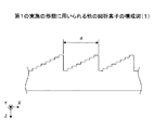
次に、ホールアレイ15について説明する。図12は、本実施の形態における分光測定装置において用いられているホールアレイ15の構造を示すものである。ホールアレイ15は、全体を構成する遮光部31に光を透過する複数の開口部32が設けられたものである。開口部32は、矩形のスリット状の形状で形成されており、所定の間隔で一列に配列されている。尚、開口部32における形状は矩形の形状に限定されるものではなく、楕円や円形又は、その他の形状であってもよい。
Next, the
ホールアレイ15における一つの開口部32を通過した光線は、図4における破線に示されるように、回折素子17により分光されラインセンサ18におけるN個の画素21に各々入射する。即ち、ホールアレイ15における一つの開口部32が、ラインセンサ18における一つの分光センサ部22に対応している。よって、ホールアレイ15における一つの開口部32を通過した光は、分光されラインセンサ18における一つの分光センサ部22におけるN個の画素21に各々入射する。これにより分光センサ部22におけるN個の画素21においては、各々の光の波長帯ごとの光量を電気信号として検出することができる。
As shown by the broken line in FIG. 4, the light beam that has passed through one
ホールアレイ15は、具体的には、表面を黒化処理した金属板に開口部32となる開口を設けた構成のものや、ガラス基板の表面に開口部32となる領域以外にクロム膜やカーボン含有樹脂等の黒色部材からなる膜が形成されている構成のものである。
Specifically, the
図13には、他の構成のホールアレイの構造を示す。このホールアレイは、全体を構成する遮光部33に、幅の狭い開口部34が一列に形成された第1の領域41と、次に幅の広い開口部35が一列に形成された第2の領域42と、最も幅の広い開口部36が一列に形成された第3の領域43とを有している。このホールアレイは、矢印Aに示す方向に移動させることにより、入射光が第1の領域41、第2の領域42及び第3の領域43のいずれか1つに入射するように切換えることが可能である。このように、ホールアレイにおける第1の領域41、第2の領域42及び第3の領域43のいずれかに切換えることにより、所望の波長分解能に応じた分光特性を得ることができる。
FIG. 13 shows the structure of a hole array having another configuration. In the hole array, a
以上より、本実施の形態における分光測定装置では、容易に高精度の分光特性を取得することができ、また、像高に依存することなく、精度の高い分光特性を取得することができる。 As described above, the spectroscopic measurement apparatus according to the present embodiment can easily acquire highly accurate spectral characteristics, and can acquire highly accurate spectral characteristics without depending on the image height.
ところで、本実施の形態における分光測定装置においては、ラインセンサ18の分光センサ部22を構成する画素21の数Nが多いほど、分光特性を詳細に得ることができる。しかしながら、ラインセンサ18における画素数には限界があり、画素21の数Nが増加することにより、分光センサ部22の数は減少してしまう。
By the way, in the spectroscopic measurement apparatus according to the present embodiment, the spectral characteristics can be obtained in more detail as the number N of the
よって、本実施の形態における分光測定装置では、特に測色を目的とする場合においては、画素21の数Nを最小に抑えてウィナー推定等の推定手段によって分光分布の推定を行う処理を行うことが好ましい。
Therefore, in the spectroscopic measurement apparatus according to the present embodiment, particularly for the purpose of color measurement, the number N of
一例として、一つの分光センサ部22の出力より、分光分布を推定する方法について説明する。一つの分光センサ部22を構成しているN個の画素21からの信号出力vi(i=1〜N)を格納した行ベクトルvと、変換行列Gから、各々の波長帯における分光反射率(例えば、400〜700nmで、10nmピッチで分離した31個)を格納した行ベクトルrは、下記の(1)に示す式により表される。
As an example, a method for estimating the spectral distribution from the output of one
r=Gv・・・・・・・・・(1)
変換行列Gは、予め分光分布が既知である多数(n個)のサンプルに対して、分光分布を格納した行列Rと、同様のサンプルを本実施の形態における分光測定装置により測定したときの行ベクトルvを格納した行列Vより、最小二乗法をもちいて誤差の2乗ノルム‖・‖2を最小化することにより求めることが可能である。
r = Gv (1)
The transformation matrix G includes a matrix R in which the spectral distribution is stored for a large number (n) of samples whose spectral distributions are known in advance, and a row when the same sample is measured by the spectroscopic measurement apparatus according to the present embodiment. It can be obtained from the matrix V storing the vector v by minimizing the square norm of error ‖ · ‖2 using the least square method.
R=[r1、r2、・・・・・、rn]・・・・・(2)
V=[v1、v2、・・・・・、vn]・・・・・(3)
e=‖R−GV‖2→min・・・・・・・・・・(4)
Vを説明変数、Rを目的変数としたVからRへの回帰式の回帰係数行列である変換行列Gは、行列Vの二乗最小ノルム解を与えるMoore-Penroseの一般化逆行列を用いて、下記の(5)に示す式により表される。
R = [r1, r2,..., Rn] (2)
V = [v1, v2,..., Vn] (3)
e = ‖R-GV‖2 → min (4)
A transformation matrix G, which is a regression coefficient matrix of a regression equation from V to R, where V is an explanatory variable and R is an objective variable, uses a Moore-Penrose generalized inverse matrix that gives a least-squares norm solution of the matrix V. It is represented by the formula shown in the following (5).
G=RVT(VVT)−1・・・・・・・・・・・・・(5)
ここで、上付きTは行列の転置を意味し、上付−1は逆行列を意味している。これにより算出された変換行列Gを記憶させておき、実際の測定時には変換行列Gと信号出力の行ベクトルvとの積により、任意の被測定物の分光分布の行ベクトルrを推定することができる。
G = RV T (VV T ) −1 (5)
Here, the superscript T means transposition of a matrix, and the superscript -1 means an inverse matrix. The conversion matrix G calculated in this way is stored, and the row vector r of the spectral distribution of an arbitrary object to be measured can be estimated by the product of the conversion matrix G and the signal output row vector v during actual measurement. it can.
更に、本実施の形態における分光測定装置を用いて、電子写真方式による画像形成装置により出力したトナーにより形成されるカラー画像について分光分布を行った場合のシミュレーションを行った結果について説明する。シミュレーションでは、分光センサ部22を構成する画素21の数Nを変化させた場合の測色結果と、より高精度の分光分析装置により得られる測色結果との色差ΔEを求めた。図14は、このシミュレーションにより得られた結果であり、ラインセンサ17における分光センサ部22を構成する画素21の数Nと、色差ΔEとの関係を示すものである。図14に示されるように、Nの値が6以上において、色差が低くなり、本実施の形態における分光測定装置により得られたものとの誤差が小さいことが解る。このように、トナーにより形成されるカラー画像においては、本実施の形態における分光測定装置においては、Nの値を6以上とすることが好ましい。
Further, a description will be given of a result of a simulation performed when spectral distribution is performed on a color image formed by toner output from an electrophotographic image forming apparatus using the spectroscopic measurement apparatus according to the present embodiment. In the simulation, the color difference ΔE between the color measurement result when the number N of the
〔第2の実施の形態〕
次に、第2の実施の形態について説明する。本実施の形態は、分光測定装置に用いられる回折素子17の構造に関するものであり、第1の実施の形態における分光測定装置に用いられるものである。
[Second Embodiment]
Next, a second embodiment will be described. The present embodiment relates to the structure of the
回折素子17が、屈折率n(λ)を有する材料により、鋸歯形状の高さhで形成されており、回折素子17に入射する主光線の入射の角度θinとした場合、回折効率ηは、数3に示す式で表される。
When the
数3に示される式より、回折素子17に入射する光の回折効率ηは波長依存性を有しており、また、入射角度θinに対しても依存性を有するものである。前述したように、回折素子17に入射する主光線の入射角度θinは、結像光学系16によって結像される像の像高に応じて異なっており、この像高に応じて回折効率ηの変動が生じ、ラインセンサ18に入射する光の分光特性に違いが生じてしまう。
From the equation shown in Equation 3, the diffraction efficiency η of the light incident on the
このため、本実施の形態における回折素子17では、回折効率ηが略一定の値となるように、主光線の入射角度θinに応じて、即ち、結像光学系16によって結像される像の像高に応じて、回折素子17における回折格子の高さhを変化させたものである。
For this reason, in the
具体的には、図15に示すように、主光線の入射角度θinに対し、回折素子17における回折格子の高さhを変化させる。尚、図15における横軸の下段は、前述したラインセンサ用レンズを用いた場合においては、±10°の角度θinが、±30mmの像高に対応するため、回折素子17における位置を示すものである。図15に示す場合では、波長が0.53μmの光に対して回折効率ηが最適となるように回折素子17における回折格子の高さhを形成したものである。本実施の形態において用いられる回折素子17は、中心部における高さが、周辺部における高さよりも高い構造のものである。尚、数3に示す式により得られる回折効率ηは、近似的な値であるため、厳密結合波解析(RCWA)法等による、より厳密な解析手法を用いて解析を行い、高さhを定めることがより好ましい。尚、回折格子における高さhは連続的に変化している場合に限定されず、階段的に変化している構成であってもよい。
Specifically, as shown in FIG. 15, the height h of the diffraction grating in the
本実施の形態における分光測定装置では、回折素子17における回折格子の高さhを結像光学系16によって結像される像の像高に対応して変化させることにより、ラインセンサ18における各々の分光センサ部22に略同一の回折効率の回折光を入射させることが可能となり、結像光学系16によって結像される像の像高に依存することなく、高精度の分光特性を得ることが可能である。
In the spectroscopic measurement apparatus according to the present embodiment, the height h of the diffraction grating in the
〔第3の実施の形態〕
次に、第3の実施の形態について説明する。本実施の形態における分光測定装置は、回折素子17により生じる0次光等がラインセンサ18における画素21に入射することを防いだ構成のものであり、より高精度の分光特性を得ることのできる分光測定装置である。
[Third Embodiment]
Next, a third embodiment will be described. The spectroscopic measurement apparatus according to the present embodiment has a configuration in which 0th-order light or the like generated by the
本実施の形態における分光測定装置は、図4における矢印Bに示す回折素子17の回折格子ベクトル方向と、ラインセンサ18における画素21の配列方向とが、非平行となる(平行とはならない)構成のものである。このように非平行に配置することにより、回折素子17において発生する0次光や+1次回折光以外の回折光がラインセンサ18における画素21に入射することを防ぐことができる。尚、ラインセンサ18は1次元方向に画素21が配列されている。
In the spectroscopic measurement apparatus according to the present embodiment, the diffraction grating vector direction of the
図16に基づき本実施の形態における分光測定装置を説明する。図16は、ラインセンサ18に入射する光の入射面側からみたラインセンサ18に入射する光を示す図である。図16に示されるように、回折素子17により、+1次回折光(+1次光)以外に、0次光、−1次回折光(−1次光)、+2次回折光(+2次光)、−2次回折光(−2次光)等が発生する。0次光、−1次回折光、+2次回折光、−2次回折光等は、+1次回折光に比べて強度は弱いが、ラインセンサ18の画素21に入射することにより、分光特性の精度を低下させてしまう。
A spectroscopic measurement apparatus according to the present embodiment will be described with reference to FIG. FIG. 16 is a diagram illustrating light incident on the
本実施の形態では、回折素子17の回折格子ベクトル方向と、ラインセンサ18における画素21の配列方向とが、角度α傾いた状態で設置されている。即ち、図1の紙面であるXZ面に対し、X軸と回折素子17の回折格子ベクトル方向とのなす角がαとなるように設置されている。尚、ラインセンサ18の画素21の配列方向は、X軸方向に配列されるよう設置されているものとする。
In the present embodiment, the diffraction grating vector direction of the
このように、ラインセンサ18と回折素子17を配置することにより、回折素子17により分光された+1次回折光のみをラインセンサ18に配列されている画素21に入射させることができ、0次光、−1次回折光、+2次回折光、−2次回折光等の光が入射することを防ぐことができる。
Thus, by arranging the
尚、ラインセンサ18と回折素子17との間には、ラインセンサ18に配列されている画素21において、+1次回折光のみが入射するような開口部を有する遮光板等を設けてもよい。
A light shielding plate or the like having an opening through which only the + 1st order diffracted light is incident may be provided between the
〔第4の実施の形態〕
次に、第4の実施の形態について説明する。本実施の形態は、第3の実施の形態をさらに改良した構成の分光測定装置である。
[Fourth Embodiment]
Next, a fourth embodiment will be described. The present embodiment is a spectroscopic measurement apparatus having a configuration obtained by further improving the third embodiment.
ところで、回折素子17の回折格子ベクトルが、XZ面に対して、X軸とのなす角が角度αとなるような状態で設置されている場合、回折素子17に入射する光の入射角度θinは、結像光学系16によって結像される像の像高に応じて異なるものとなり、ラインセンサ18に入射する光は、Y方向において位置ズレが生じてしまう可能性がある。
By the way, when the diffraction grating vector of the
図17には、αが50°、距離tが0.927mm、回折素子17における回折格子の周期dが約3.333μmである場合において、波長が530nmの+1次回折光がラインセンサ18に入射した場合の入射角度θinとY方向の位置ay(λ)との関係を示す。尚、Y方向の原点位置は、0次光の位置としている。
In FIG. 17, + 1st order diffracted light having a wavelength of 530 nm is incident on the
+1次回折光の位置がY方向にずれることにより、+1次回折光が正確にラインセンサ18における各々の画素21に入射しないといった問題や、±2次回折光がラインセンサ18における各々の画素21に入射してしまうといった問題が生じ、高精度の分光特性を得ることが困難となる。
Since the position of the + 1st order diffracted light is shifted in the Y direction, the problem that the + 1st order diffracted light does not accurately enter each
よって、本実施の形態における分光測定装置では、回折素子17における回折格子ベクトル、即ち、角度αを像高に対応させて変化させた構成のものである。具体的には、図18に示すように、回折素子17において、光の入射角度θinに応じて角度αを変化させる。尚、図10における横軸の下段は、前述したラインセンサ用レンズを用いた場合においては、±10°の角度θinが、±30mmの像高に対応するため、回折素子17における位置を示すものである。
Therefore, the spectroscopic measurement apparatus according to the present embodiment has a configuration in which the diffraction grating vector in the
図19は、図18に示す回折素子17において、光の波長が530nmの場合における入射角度θinとY方向の光の入射位置ay(λ)との関係を示すものである。図19に示されるように、図18に示す回折素子17を用いることにより、角度θinに依存することなくY方向の光の入射位置ay(λ)を略一定にすることができる。このように、回折素子17における回折格子ベクトル方向を結像光学系16によって結像される像の像高に対応させて変化させることにより、結像光学系16によって結像される像の像高に依存することなく、Y方向の光の入射位置ay(λ)を略一定にすることができる。
FIG. 19 shows the relationship between the incident angle θ in and the light incident position a y (λ) in the Y direction when the light wavelength is 530 nm in the
これにより、本実施の形態における分光測定装置では、結像光学系16によって結像される像の像高に依存することなく、Y方向の光の入射位置ay(λ)を略一定にすることができ、高精度の分光特性を測定することが可能となる。
Thereby, in the spectroscopic measurement apparatus according to the present embodiment, the incident position a y (λ) of the light in the Y direction is made substantially constant without depending on the image height of the image formed by the imaging
更に、本実施の形態における回折素子17は、回折格子ベクトルの方向のみではなく、図10に示すような、回折素子17における回折格子の高さhも変化させるものであってもよい。回折素子17における周期d、高さh、角度αを像高に対応させて最適化することにより、より高精度の分光特性を得ることが可能となる。
Furthermore, the
〔第5の実施の形態〕
次に、第5の実施の形態について説明する。本実施の形態は、第1から第4の実施の形態における分光測定装置を用いた画像評価装置である。
[Fifth Embodiment]
Next, a fifth embodiment will be described. This embodiment is an image evaluation apparatus using the spectroscopic measurement apparatus in the first to fourth embodiments.
図20に基づき本実施の形態における画像評価装置50について説明する。本実施の形態における画像評価装置50は、紙等の画像担持媒体11に画像形成装置等により形成された画像を紙等の全幅にわたり評価することが可能な装置である。本実施の形態における画像評価装置50は、図1に示す分光測定装置を複数設けた構成のものである。具体的には、一組の結像光学系16、回折素子17及びラインセンサ18からなる測定部51を複数設けたものであり、各々の測定部51は、処理部52に接続されている。このような構成にすることにより、紙等の画像担持媒体11において、広い範囲において分光特性を測定することができる。尚、本実施の形態における画像評価装置50には、不図示の紙搬送機構を有しており、図20における紙面の奥行き方向に、紙等の画像担持媒体11を搬送することが可能である。また、処理部52は、複数の測定部51における測定結果、及び、不図示の紙搬送機構に設けられているエンコーダーセンサからの速度情報に基づき、紙等の画像担持媒体11の全面における画像の分光特性を算出し、さらには、この分光特性に基づき紙等の画像担持媒体11に形成された画像の評価を行う機能を有している。
The
〔第6の実施の形態〕
次に、第6の実施の形態について説明する。本実施の形態は、第5の実施の形態における画像評価装置50を有する画像形成装置である。
[Sixth Embodiment]
Next, a sixth embodiment will be described. The present embodiment is an image forming apparatus having the
図21に基づき本実施の形態における画像形成装置について説明する。本実施の形態における画像形成装置は、給紙トレイ61a及び61b、給紙ローラ62、コントローラ63、走査光学系64、感光体ユニット65、中間転写体66、定着ユニット67、排紙ローラ68を有しており、定着ユニット67と排紙ローラ68との間に、第5の実施の形態における画像評価装置50を設置した構成のものである。尚、本実施の形態における画像形成装置においては、画像評価装置50以外の部材により、画像形成部が構成される。
The image forming apparatus according to the present embodiment will be described with reference to FIG. The image forming apparatus according to the present embodiment includes
本実施の形態における画像形成装置では、給紙トレイ61a及び61bから画像担持媒体である紙69を給紙ローラ62により搬送する。一方、走査光学系64により感光体ユニット65の感光体に露光され、色材が付与されて現像される。色材により現像された画像は中間転写体66に転写され、更に、中間転写体66より紙69に転写される。紙69に転写された画像は、定着ユニット67により定着され、画像形成された紙69として排紙ローラ68により排紙される。
In the image forming apparatus according to the present embodiment, the
本実施の形態における画像形成装置では、画像評価装置50により紙69に定着されている画像について分光測定に基づく画像評価を行い、この画像評価の結果をコントローラ63に伝達し、画像評価に基づいて最適な画像形成を行うことができるものである。
In the image forming apparatus according to the present embodiment, image evaluation based on spectroscopic measurement is performed on the image fixed on the
よって、本実施の形態における画像形成装置では、形成される画像の全体において色変動等のない高品位な画像を提供することが可能となり、色の自動キャリブレーションを可能とすることから、安定的に紙等の画像担持媒体に画像形成を行うことが可能となる。また、形成された画像の全域において画像情報を取得することができるものであるため、検品や印刷データの保存等を可能とし、信頼性の高い画像形成を行うことが可能となる。 Therefore, the image forming apparatus according to the present embodiment can provide a high-quality image without color variation or the like in the entire formed image, and enables automatic color calibration. In addition, it is possible to form an image on an image bearing medium such as paper. Further, since the image information can be acquired over the entire area of the formed image, it is possible to store inspections and print data, and to perform highly reliable image formation.
本実施の形態では、トナーを用いた電子写真方式の画像形成装置について説明したが、他の電子写真方式の画像形成装置、インクジェット方式の画像形成装置、オフライン印刷やカラープルーフ等においても適用することが可能である。 In this embodiment, an electrophotographic image forming apparatus using toner has been described. However, the present invention can be applied to other electrophotographic image forming apparatuses, inkjet image forming apparatuses, offline printing, color proofing, and the like. Is possible.
以上、本発明の実施に係る形態について説明したが、上記内容は、発明の内容を限定するものではなく、特許請求の範囲に記載された範囲を逸脱することなく、上述した実施の形態に種々の変形及び置換を加えることが可能である。 As mentioned above, although the form which concerns on implementation of this invention was demonstrated, the said content does not limit the content of invention, and it does not deviate from the range described in the claim, but various in the embodiment mentioned above. It is possible to add variations and substitutions.
11 画像担持媒体
12 ライン照明光源
13 レンズ
14 セルフォックレンズ
15 ホールアレイ
16 結像光学系
17 回折素子
18 ラインセンサ
50 画像評価装置
51 測定部
52 処理部
61a、61b 用紙トレイ
62 給紙ローラ
63 コントローラ
64 走査光学系
65 感光体ユニット
66 中間転写体
67 定着ユニット
68 排紙ローラ
69 紙
DESCRIPTION OF
Claims (8)
前記光照射部から画像担持媒体に照射された光の反射光を通過する複数の開口部を含むホールアレイと、
前記ホールアレイを通過した光を結像する結像光学系と、
前記結像光学系で結像された光を回折する回折素子と、
前記回折素子により回折された光を複数の画素を含む分光センサ部で各々受光する受光部と、
を有し、
前記回折素子における回折格子の配列方向は、各々の前記開口部を通過した光が、各々前記分光センサ部における画素に入射するように、回折格子における構造が、前記結像光学系で結像された光が回折素子へ入射する角度に対応して、変化するように形成されていることを特徴とする分光測定装置。 A light irradiation unit for irradiating the image bearing medium with light;
A hole array including a plurality of openings through which reflected light of the light irradiated to the image bearing medium from the light irradiation unit;
An imaging optical system for imaging light that has passed through the hole array;
A diffractive element that diffracts the light imaged by the imaging optical system;
A light receiving unit that receives light diffracted by the diffraction element by a spectroscopic sensor unit including a plurality of pixels, and
Have
The structure of the diffraction grating is imaged by the imaging optical system so that the light passing through each of the openings enters each pixel in the spectroscopic sensor unit. The spectroscopic measurement device is characterized in that it is formed to change in accordance with the angle at which the incident light enters the diffraction element.
前記受光部は、所定の数の画素ごとに複数の分光センサ部が形成されており、
前記回折素子における前記周期は、前記複数の開口部を通過した光が、各々前記分光センサ部に入射するように形成されていることを特徴とする請求項1に記載の分光測定装置。 The diffraction element has a sawtooth and staircase structure periodically formed on the surface, and a sawtooth and staircase structure is periodic at the interface between two members having different refractive indexes. Or a structure having a refractive index that is periodically formed,
The light receiving unit is formed with a plurality of spectral sensor units for each predetermined number of pixels,
The spectroscopic measurement apparatus according to claim 1, wherein the period of the diffraction element is formed such that light that has passed through the plurality of openings is incident on the spectroscopic sensor unit.
前記受光部は、所定の数の画素ごとに複数の分光センサ部が形成されており、
前記鋸波形状又は階段形状の構造の部分における高さは、前記複数の開口部を通過した光が、各々前記分光センサ部に入射するように形成されていることを特徴とする請求項1に記載の分光測定装置。 The diffraction element has a sawtooth or staircase structure periodically formed on the surface, or a sawtooth or staircase structure on an interface between two members having different refractive indexes. Is formed periodically,
The light receiving unit is formed with a plurality of spectral sensor units for each predetermined number of pixels,
The height of the sawtooth or stepped structure is formed such that light that has passed through the plurality of openings is incident on the spectroscopic sensor unit. The spectroscopic measurement apparatus described.
前記回折素子により回折された+1次回折光であることを特徴とする請求項1から4のいずれかに記載の分光測定装置。 The light incident on the light receiving unit is
5. The spectroscopic measurement apparatus according to claim 1, wherein the spectroscopic measurement apparatus is + 1st order diffracted light diffracted by the diffraction element.
請求項1から6のいずれかに記載の分光測定装置と、
前記分光測定装置により得られた分光特性に基づき、前記画像における画像評価を行う処理部と、
を有することを特徴とする画像評価装置。 In an image evaluation apparatus for evaluating the color of an image formed in a plurality of colors on an image bearing medium,
A spectroscopic measurement device according to any one of claims 1 to 6,
A processing unit that performs image evaluation on the image based on the spectral characteristics obtained by the spectroscopic measurement device;
An image evaluation apparatus comprising:
前記画像担持媒体に画像を形成する画像形成部と、
を有することを特徴とする画像形成装置。 An image evaluation apparatus according to claim 7;
An image forming unit that forms an image on the image bearing medium;
An image forming apparatus comprising:
Priority Applications (3)
| Application Number | Priority Date | Filing Date | Title |
|---|---|---|---|
| JP2009253498A JP5609068B2 (en) | 2009-11-04 | 2009-11-04 | Spectrometer, image evaluation apparatus, and image forming apparatus |
| US12/901,280 US8363217B2 (en) | 2009-11-04 | 2010-10-08 | Spectrometric measurement apparatus, image evaluation apparatus, and image forming apparatus |
| EP10189526.6A EP2320205B1 (en) | 2009-11-04 | 2010-10-29 | Spectrometric measurement apparatus, image evaluation apparatus, and image forming apparatus |
Applications Claiming Priority (1)
| Application Number | Priority Date | Filing Date | Title |
|---|---|---|---|
| JP2009253498A JP5609068B2 (en) | 2009-11-04 | 2009-11-04 | Spectrometer, image evaluation apparatus, and image forming apparatus |
Publications (3)
| Publication Number | Publication Date |
|---|---|
| JP2011099718A JP2011099718A (en) | 2011-05-19 |
| JP2011099718A5 JP2011099718A5 (en) | 2012-09-06 |
| JP5609068B2 true JP5609068B2 (en) | 2014-10-22 |
Family
ID=43480458
Family Applications (1)
| Application Number | Title | Priority Date | Filing Date |
|---|---|---|---|
| JP2009253498A Expired - Fee Related JP5609068B2 (en) | 2009-11-04 | 2009-11-04 | Spectrometer, image evaluation apparatus, and image forming apparatus |
Country Status (3)
| Country | Link |
|---|---|
| US (1) | US8363217B2 (en) |
| EP (1) | EP2320205B1 (en) |
| JP (1) | JP5609068B2 (en) |
Families Citing this family (20)
| Publication number | Priority date | Publication date | Assignee | Title |
|---|---|---|---|---|
| JP5609611B2 (en) * | 2010-03-11 | 2014-10-22 | 株式会社リコー | Spectral characteristic acquisition device, image evaluation device, and image forming device |
| JP5884347B2 (en) | 2011-09-12 | 2016-03-15 | 株式会社リコー | Spectral characteristic acquisition apparatus, spectral characteristic acquisition method, image evaluation apparatus, and image forming apparatus |
| JP2013142595A (en) * | 2012-01-10 | 2013-07-22 | Ricoh Co Ltd | Spectroscopic characteristic acquisition device, image evaluation device, and image forming apparatus |
| JP5880053B2 (en) | 2012-01-12 | 2016-03-08 | 株式会社リコー | Spectral characteristic acquisition apparatus and image forming apparatus |
| JP5938911B2 (en) * | 2012-01-12 | 2016-06-22 | セイコーエプソン株式会社 | Spectral measurement method, spectroscopic instrument, and conversion matrix generation method |
| JP5938910B2 (en) * | 2012-01-12 | 2016-06-22 | セイコーエプソン株式会社 | Spectral measurement method, spectroscopic instrument, and conversion matrix generation method |
| JP5834938B2 (en) | 2012-01-17 | 2015-12-24 | 株式会社リコー | Spectral characteristic acquisition apparatus, image evaluation apparatus, image forming apparatus, and spectral characteristic acquisition method |
| JP5910989B2 (en) | 2012-03-09 | 2016-04-27 | 株式会社リコー | Spectroscopic measurement apparatus, image evaluation apparatus, and image forming apparatus |
| JP6051543B2 (en) * | 2012-03-09 | 2016-12-27 | 株式会社リコー | Spectroscopic measurement apparatus, image evaluation apparatus, and image forming apparatus |
| JP6094857B2 (en) * | 2012-10-31 | 2017-03-15 | 株式会社リコー | Reading lens and spectrometer |
| JP5842849B2 (en) * | 2013-03-27 | 2016-01-13 | セイコーエプソン株式会社 | Optical spectrum conversion method and optical spectrum converter |
| JP6311267B2 (en) * | 2013-05-10 | 2018-04-18 | 株式会社リコー | Spectral characteristic acquisition device, image evaluation device, image forming device |
| US10175396B2 (en) * | 2014-12-11 | 2019-01-08 | Rambus Inc. | Ultra-miniature wide-angle lensless CMOS visual edge localizer |
| US11514526B1 (en) * | 2016-05-17 | 2022-11-29 | Liberty Mutual Insurance Company | Systems and methods for property damage restoration predictions based upon processed digital images |
| JP6988512B2 (en) | 2018-01-24 | 2022-01-05 | 株式会社リコー | Spectroscopic property acquisition device, image forming device, image forming system |
| JP7095304B2 (en) | 2018-02-15 | 2022-07-05 | 株式会社リコー | Spectral characteristic acquisition device, image forming device, image forming system, image forming device management system, and image forming device management method |
| FR3079612B1 (en) * | 2018-03-29 | 2021-06-04 | Eldim | OPTICAL DEVICE ALLOWING SIMULTANEOUS MEASUREMENT OF THE ANGULAR AND SPECTRAL EMISSION OF AN OBJECT |
| JP7087735B2 (en) | 2018-06-29 | 2022-06-21 | 株式会社リコー | Spectroscopic property acquisition device, image forming device, and management system for image forming device |
| JP2020153814A (en) | 2019-03-20 | 2020-09-24 | 株式会社リコー | Spectral characteristic acquisition device |
| WO2022221101A1 (en) * | 2021-04-13 | 2022-10-20 | Oak Analytics Inc. | Optical spectrometer with high-efficiency optical coupling |
Family Cites Families (16)
| Publication number | Priority date | Publication date | Assignee | Title |
|---|---|---|---|---|
| JPH02216019A (en) * | 1989-02-17 | 1990-08-28 | Hitachi Ltd | Monochrometer |
| JP3566334B2 (en) * | 1994-03-25 | 2004-09-15 | キヤノン株式会社 | Image processing apparatus and method |
| US5847877A (en) * | 1994-09-12 | 1998-12-08 | Olympus Optical Co., Ltd. | Diffractive optical element |
| JP3717555B2 (en) | 1994-09-12 | 2005-11-16 | オリンパス株式会社 | Diffractive optical element |
| JP3568334B2 (en) | 1996-10-31 | 2004-09-22 | 横浜ゴム株式会社 | Pneumatic tire and method of manufacturing the same |
| JPH11313334A (en) | 1998-04-27 | 1999-11-09 | Nippon Hoso Kyokai <Nhk> | Solid-state image pickup device |
| JP2001264174A (en) * | 2000-03-16 | 2001-09-26 | Minolta Co Ltd | Apparatus for measuring reflecting characteristics |
| EP1344193B1 (en) * | 2000-12-21 | 2007-07-04 | De La Rue International Limited | Optical sensor device and method for spectral analysis |
| JP2002310799A (en) | 2001-04-16 | 2002-10-23 | Dac Engineering Kk | Method and device for detecting concentration of color ink of printed matter |
| JP2003139702A (en) | 2001-10-31 | 2003-05-14 | Web Tec Kk | Device for detecting density of multi-color printed image on printing sheet |
| WO2003038383A1 (en) | 2001-10-31 | 2003-05-08 | Webtech Co., Ltd. | Method and device for detecting hue and density of multicolor sheet |
| US8174694B2 (en) * | 2001-12-21 | 2012-05-08 | Bodkin Design And Engineering Llc | Hyperspectral imaging systems |
| US6975949B2 (en) | 2004-04-27 | 2005-12-13 | Xerox Corporation | Full width array scanning spectrophotometer |
| WO2006045621A1 (en) | 2004-10-28 | 2006-05-04 | Gretagmacbeth Ag | Measurement system and scanning device for the photoelectric measurement of a measurement object pixel by pixel |
| EP1694047B1 (en) * | 2005-02-16 | 2020-03-18 | X-Rite Switzerland GmbH | Lighting system for a colour measuring device |
| JP5476733B2 (en) | 2009-02-17 | 2014-04-23 | 株式会社リコー | Image evaluation apparatus, image evaluation method, and image forming apparatus |
-
2009
- 2009-11-04 JP JP2009253498A patent/JP5609068B2/en not_active Expired - Fee Related
-
2010
- 2010-10-08 US US12/901,280 patent/US8363217B2/en active Active
- 2010-10-29 EP EP10189526.6A patent/EP2320205B1/en active Active
Also Published As
| Publication number | Publication date |
|---|---|
| JP2011099718A (en) | 2011-05-19 |
| EP2320205A1 (en) | 2011-05-11 |
| US8363217B2 (en) | 2013-01-29 |
| EP2320205B1 (en) | 2020-06-03 |
| US20110106472A1 (en) | 2011-05-05 |
Similar Documents
| Publication | Publication Date | Title |
|---|---|---|
| JP5609068B2 (en) | Spectrometer, image evaluation apparatus, and image forming apparatus | |
| US9222833B2 (en) | Spectral characteristic obtaining apparatus, image evaluation apparatus and image forming apparatus | |
| JP5609611B2 (en) | Spectral characteristic acquisition device, image evaluation device, and image forming device | |
| JP5655437B2 (en) | Spectral characteristics acquisition device | |
| JP5884347B2 (en) | Spectral characteristic acquisition apparatus, spectral characteristic acquisition method, image evaluation apparatus, and image forming apparatus | |
| JP6232831B2 (en) | Spectral characteristic acquisition device, image evaluation device, and image forming device | |
| US8462406B2 (en) | Spectral colorimetric apparatus and image forming apparatus using the same | |
| JP5880053B2 (en) | Spectral characteristic acquisition apparatus and image forming apparatus | |
| JP2010261861A (en) | Spectral characteristics acquisition apparatus, image evaluation apparatus, and image forming apparatus | |
| JP2013061175A (en) | Spectral characteristic acquisition device and spectral characteristic acquisition method, image evaluation device, and image formation device | |
| JP5499767B2 (en) | Image characteristic measuring method, image characteristic measuring apparatus, image evaluation apparatus, and image forming apparatus | |
| JP2016102679A (en) | Spectroscopic measurement device | |
| JP5644296B2 (en) | Spectral characteristic acquisition device, image evaluation device, and image forming device | |
| JP2018017670A (en) | Spectral characteristic acquisition device, image evaluation device and image formation device | |
| JP5652183B2 (en) | Image characteristic measuring apparatus and image forming apparatus | |
| JP5923979B2 (en) | Spectral characteristic acquisition device, image evaluation device, and image forming device | |
| US20230291842A1 (en) | Information processing apparatus, abnormality detection method, storage medium, and information processing system | |
| JP2023131099A (en) | Information processing device, program, anomaly detection method, and information processing system | |
| JP2015036659A (en) | Spectroscopic characteristic acquisition device, image evaluation device, and image forming apparatus | |
| JP2013142595A (en) | Spectroscopic characteristic acquisition device, image evaluation device, and image forming apparatus | |
| JP2016008897A (en) | Image characteristics measurement apparatus, image evaluation apparatus, and image forming apparatus |
Legal Events
| Date | Code | Title | Description |
|---|---|---|---|
| A521 | Request for written amendment filed |
Free format text: JAPANESE INTERMEDIATE CODE: A523 Effective date: 20120719 |
|
| A621 | Written request for application examination |
Free format text: JAPANESE INTERMEDIATE CODE: A621 Effective date: 20120719 |
|
| A977 | Report on retrieval |
Free format text: JAPANESE INTERMEDIATE CODE: A971007 Effective date: 20130628 |
|
| A131 | Notification of reasons for refusal |
Free format text: JAPANESE INTERMEDIATE CODE: A131 Effective date: 20130924 |
|
| A131 | Notification of reasons for refusal |
Free format text: JAPANESE INTERMEDIATE CODE: A131 Effective date: 20140624 |
|
| A521 | Request for written amendment filed |
Free format text: JAPANESE INTERMEDIATE CODE: A523 Effective date: 20140711 |
|
| TRDD | Decision of grant or rejection written | ||
| A01 | Written decision to grant a patent or to grant a registration (utility model) |
Free format text: JAPANESE INTERMEDIATE CODE: A01 Effective date: 20140805 |
|
| A61 | First payment of annual fees (during grant procedure) |
Free format text: JAPANESE INTERMEDIATE CODE: A61 Effective date: 20140818 |
|
| R151 | Written notification of patent or utility model registration |
Ref document number: 5609068 Country of ref document: JP Free format text: JAPANESE INTERMEDIATE CODE: R151 |
|
| LAPS | Cancellation because of no payment of annual fees |