JP5590829B2 - Surface emitting laser, surface emitting laser array, and image forming apparatus - Google Patents
Surface emitting laser, surface emitting laser array, and image forming apparatus Download PDFInfo
- Publication number
- JP5590829B2 JP5590829B2 JP2009159130A JP2009159130A JP5590829B2 JP 5590829 B2 JP5590829 B2 JP 5590829B2 JP 2009159130 A JP2009159130 A JP 2009159130A JP 2009159130 A JP2009159130 A JP 2009159130A JP 5590829 B2 JP5590829 B2 JP 5590829B2
- Authority
- JP
- Japan
- Prior art keywords
- layer
- emitting laser
- surface emitting
- barrier structure
- cladding layer
- Prior art date
- Legal status (The legal status is an assumption and is not a legal conclusion. Google has not performed a legal analysis and makes no representation as to the accuracy of the status listed.)
- Expired - Fee Related
Links
Images


Classifications
-
- H—ELECTRICITY
- H01—ELECTRIC ELEMENTS
- H01S—DEVICES USING THE PROCESS OF LIGHT AMPLIFICATION BY STIMULATED EMISSION OF RADIATION [LASER] TO AMPLIFY OR GENERATE LIGHT; DEVICES USING STIMULATED EMISSION OF ELECTROMAGNETIC RADIATION IN WAVE RANGES OTHER THAN OPTICAL
- H01S5/00—Semiconductor lasers
- H01S5/10—Construction or shape of the optical resonator, e.g. extended or external cavity, coupled cavities, bent-guide, varying width, thickness or composition of the active region
- H01S5/18—Surface-emitting [SE] lasers, e.g. having both horizontal and vertical cavities
- H01S5/183—Surface-emitting [SE] lasers, e.g. having both horizontal and vertical cavities having only vertical cavities, e.g. vertical cavity surface-emitting lasers [VCSEL]
- H01S5/18308—Surface-emitting [SE] lasers, e.g. having both horizontal and vertical cavities having only vertical cavities, e.g. vertical cavity surface-emitting lasers [VCSEL] having a special structure for lateral current or light confinement
- H01S5/18311—Surface-emitting [SE] lasers, e.g. having both horizontal and vertical cavities having only vertical cavities, e.g. vertical cavity surface-emitting lasers [VCSEL] having a special structure for lateral current or light confinement using selective oxidation
-
- B—PERFORMING OPERATIONS; TRANSPORTING
- B82—NANOTECHNOLOGY
- B82Y—SPECIFIC USES OR APPLICATIONS OF NANOSTRUCTURES; MEASUREMENT OR ANALYSIS OF NANOSTRUCTURES; MANUFACTURE OR TREATMENT OF NANOSTRUCTURES
- B82Y20/00—Nanooptics, e.g. quantum optics or photonic crystals
-
- H—ELECTRICITY
- H01—ELECTRIC ELEMENTS
- H01S—DEVICES USING THE PROCESS OF LIGHT AMPLIFICATION BY STIMULATED EMISSION OF RADIATION [LASER] TO AMPLIFY OR GENERATE LIGHT; DEVICES USING STIMULATED EMISSION OF ELECTROMAGNETIC RADIATION IN WAVE RANGES OTHER THAN OPTICAL
- H01S5/00—Semiconductor lasers
- H01S5/06—Arrangements for controlling the laser output parameters, e.g. by operating on the active medium
- H01S5/065—Mode locking; Mode suppression; Mode selection ; Self pulsating
- H01S5/0651—Mode control
- H01S5/0653—Mode suppression, e.g. specific multimode
- H01S5/0655—Single transverse or lateral mode emission
-
- H—ELECTRICITY
- H01—ELECTRIC ELEMENTS
- H01S—DEVICES USING THE PROCESS OF LIGHT AMPLIFICATION BY STIMULATED EMISSION OF RADIATION [LASER] TO AMPLIFY OR GENERATE LIGHT; DEVICES USING STIMULATED EMISSION OF ELECTROMAGNETIC RADIATION IN WAVE RANGES OTHER THAN OPTICAL
- H01S5/00—Semiconductor lasers
- H01S5/20—Structure or shape of the semiconductor body to guide the optical wave ; Confining structures perpendicular to the optical axis, e.g. index or gain guiding, stripe geometry, broad area lasers, gain tailoring, transverse or lateral reflectors, special cladding structures, MQW barrier reflection layers
- H01S5/2004—Confining in the direction perpendicular to the layer structure
- H01S5/2009—Confining in the direction perpendicular to the layer structure by using electron barrier layers
-
- H—ELECTRICITY
- H01—ELECTRIC ELEMENTS
- H01S—DEVICES USING THE PROCESS OF LIGHT AMPLIFICATION BY STIMULATED EMISSION OF RADIATION [LASER] TO AMPLIFY OR GENERATE LIGHT; DEVICES USING STIMULATED EMISSION OF ELECTROMAGNETIC RADIATION IN WAVE RANGES OTHER THAN OPTICAL
- H01S5/00—Semiconductor lasers
- H01S5/30—Structure or shape of the active region; Materials used for the active region
- H01S5/34—Structure or shape of the active region; Materials used for the active region comprising quantum well or superlattice structures, e.g. single quantum well [SQW] lasers, multiple quantum well [MQW] lasers or graded index separate confinement heterostructure [GRINSCH] lasers
- H01S5/343—Structure or shape of the active region; Materials used for the active region comprising quantum well or superlattice structures, e.g. single quantum well [SQW] lasers, multiple quantum well [MQW] lasers or graded index separate confinement heterostructure [GRINSCH] lasers in AIIIBV compounds, e.g. AlGaAs-laser, InP-based laser
- H01S5/34313—Structure or shape of the active region; Materials used for the active region comprising quantum well or superlattice structures, e.g. single quantum well [SQW] lasers, multiple quantum well [MQW] lasers or graded index separate confinement heterostructure [GRINSCH] lasers in AIIIBV compounds, e.g. AlGaAs-laser, InP-based laser with a well layer having only As as V-compound, e.g. AlGaAs, InGaAs
Description
本発明は、面発光レーザ、面発光レーザアレイ及び画像形成装置に関するものである。 The present invention relates to a surface emitting laser, a surface emitting laser array, and an image forming apparatus.
垂直共振器型面発光レーザ(VCSEL:Vertical Cavity Surface Emitting Laser)は、半導体基板の面内方向に対して垂直方向にレーザ光を出射するレーザである。
面発光レーザは、縦モード特性として安定した単一モードが得られ、また端面発光レーザに比べて低しきい値、2次元アレイ化が容易、などの優れた特性を有するレーザである。そのため、面発光レーザは、光通信、光伝送用の光源、また電子写真の光源として応用が期待されている。
Vertical cavity surface emitting laser (VCSEL: V e rtical Cavity Surface Emitting Laser) is a laser for emitting a laser beam in a direction perpendicular to plane direction of the semiconductor substrate.
A surface-emitting laser is a laser that has a superior single-mode characteristics as a longitudinal mode characteristic, and has excellent characteristics such as a low threshold and a two-dimensional array that are easier than an edge-emitting laser. Therefore, the surface emitting laser is expected to be applied as a light source for optical communication and optical transmission, and as a light source for electrophotography.
ところで、このような面発光レーザにおいて、発振する横モードの制御は重要な課題であり、通信などへの応用を考えると、横モード出力は単一モード(シングルモード)であることが求められる。
そのため、従来においては、特許文献1に開示されているように、面発光レーザでは素子内部に選択酸化による電流狭窄構造を設けることにより活性層の発光領域を制限し、また同時に選択酸化部分で導波構造を形成することにより、単一横モード化を図っている。
By the way, in such a surface emitting laser, control of the transverse mode to oscillate is an important issue, and considering the application to communication, the transverse mode output is required to be a single mode (single mode).
Therefore, conventionally, as disclosed in Patent Document 1, in a surface emitting laser, a current confinement structure by selective oxidation is provided inside the element to limit the light emitting region of the active layer, and at the same time, it is guided by a selective oxidation portion. A single transverse mode is achieved by forming a wave structure.
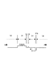
しかしながら、上記した従来例における特許文献1のような構造の面発光レーザによると、つぎのように高次横モードが生じ易くなるという課題を有している。すなわち、上記特許文献1に記載された電流狭窄構造を有する面発光レーザでは、図6(a)の模式図に示すように、光放射部の周囲に配置される電極から注入された電流が電流狭窄部で絞られる。
そのため、活性層の電流分布は、図6(b)の実線で示すように、電流狭窄領域内の周辺部に対応する付近にピークを有する。
このような電流分布により、活性層の利得も電流狭窄領域内の周辺部に対応する周辺部で増大するため、必然的に高次横モードの利得が増大し、高次横モードが強く励起される。
したがって、高い光出力を得るために注入電流を増大すると、高次横モードの発振が生じ易くなる。
However, according to the surface emitting laser having the structure as in Patent Document 1 in the above-described conventional example, there is a problem that a high-order transverse mode is likely to occur as follows. That is, in the surface emitting laser having the current confinement structure described in Patent Document 1, as shown in the schematic diagram of FIG. 6A, the current injected from the electrodes arranged around the light emitting portion is a current. Squeezed at the stenosis.
Therefore, current distribution of the active layer, as shown by the solid line in FIG. 6 (b), that have a peak near corresponding to the peripheral portion of the current confinement region.
Due to such a current distribution, the gain of the active layer also increases in the peripheral part corresponding to the peripheral part in the current confinement region, so that the high-order transverse mode gain inevitably increases and the high-order transverse mode is strongly excited. The
Therefore, when the injection current is increased in order to obtain a high light output, higher-order transverse mode oscillation is likely to occur.
本発明は、上記課題に鑑み、高次横モードの発振を抑制することが可能となる構造を有する面発光レーザ、面発光レーザアレイ及び画像形成装置を提供することを目的とする。 In view of the above problems, an object of the present invention is to provide a surface-emitting laser, a surface-emitting laser array, and an image forming apparatus having a structure capable of suppressing high-order transverse mode oscillation.
本発明は、つぎのように構成した面発光レーザ、面発光レーザアレイ及び画像形成装置を提供するものである。
本発明の面発光レーザは、
基板の上に設けられた下部DBR層と、
前記下部DBR層の上に設けられたn型の下部クラッド層と、
前記下部クラッド層の上に設けられた活性層と、
前記活性層の上に設けられた、前記活性層に注入される電流を狭窄するための電流狭窄層と、
前記電流狭窄層と前記活性層との間に設けられた、ホールキャリヤの電界印加方向への移動を抑制する障壁構造と、
前記障壁構造と前記活性層との間、および、前記電流狭窄層と前記障壁構造との間に設けられたp型の上部クラッド層と、
前記電流狭窄層の上に設けられた上部DBR層と、を有し、
前記活性層は、量子井戸層と障壁層からなる量子構造と、前記量子構造を挟むスペーサ層とで構成され、
前記下部クラッド層と前記上部クラッド層それぞれの価電子帯エネルギーは、前記スペーサ層の価電子帯エネルギーよりも低く、
前記障壁構造が、前記上部クラッド層の価電子帯エネルギーと異なる価電子帯エネルギーを有する層で構成されていることを特徴とする。
また、本発明の面発光レーザアレイは、上記した面発光レーザが、一次元または二次元に配列されていることを特徴とする。
また、本発明の画像形成装置は、上記した面発光レーザアレイを光源として構成されていることを特徴とする。
The present invention provides a surface emitting laser, a surface emitting laser array, and an image forming apparatus configured as follows.
The surface emitting laser of the present invention is
A lower DBR layer provided on the substrate,
An n-type lower cladding layer provided on the lower DBR layer ;
An active layer provided on the lower cladding layer ;
A current confinement layer provided on the active layer for constricting a current injected into the active layer;
A barrier structure that is provided between the current confinement layer and the active layer and suppresses movement of hole carriers in the electric field application direction ;
A p-type upper cladding layer provided between the barrier structure and the active layer and between the current confinement layer and the barrier structure;
An upper DBR layer provided on the current confinement layer,
The active layer is composed of a quantum structure composed of a quantum well layer and a barrier layer, and a spacer layer sandwiching the quantum structure,
The valence band energy of each of the lower cladding layer and the upper cladding layer is lower than the valence band energy of the spacer layer,
The barrier structure is formed of a layer having a valence band energy different from that of the upper cladding layer .
The surface-emitting laser array of the present invention is characterized in that the above-described surface-emitting lasers are arranged one-dimensionally or two-dimensionally.
In addition, the image forming apparatus of the present invention is configured by using the above-described surface emitting laser array as a light source.
本発明によれば、上記課題に鑑み、高次横モードの発振を抑制することが可能となる構造を有する面発光レーザ、面発光レーザアレイ及び画像形成装置を実現することができる。 According to the present invention, in view of the above problems, a surface emitting laser, a surface emitting laser array, and an image forming apparatus having a structure capable of suppressing higher-order transverse mode oscillation can be realized.
本発明では、基板上に、下部DBR層、上部DBR層、これらの間に介在する活性層、及び該活性層に注入される電流を狭窄するための電流狭窄層、を含む複数の半導体層が積層され、これらの電流狭窄構造と活性層との間にキャリヤに対する障壁構造を設ける。
すなわち、図6(b)の実線で示された電流分布を、点線で示された電流分布の形状に変化させるために、電流狭窄構造と活性層との間にキャリヤに対する障壁構造を設ける。
具体的には、電流狭窄部を通過した多数キャリヤの電界印加方向への移動を抑制する障壁構造を設け、多数キャリヤの面内方向への拡散を増大する構造とする。
これにより、電流狭窄部の周辺部に集中した電流分布をなだらかな形状に変化させることができ、高次横モードに対する利得を低減させることが可能となる。
このような構造とすることによって、高次横モードが抑制できるので、より高い電流注入レベルでも基本モード発振を維持できるので、単一モード発振を実現できる。
更に、前記電流狭窄構造をP型領域に設け、多数キャリヤをホールキャリヤとすることで、移動度が小さいホールキャリヤの面内拡散の増大を低いエネルギーの障壁構造で実現できる。
これは、上記した障壁層の導入による面発光レーザの駆動電圧の増加を抑えるのにも有効である。
更に、電流狭窄構造と活性層との間における上部クラッド層に上記障壁構造を挿入することで、キャリヤの面内方向への拡散を増大することができる。
In the present invention, a plurality of semiconductor layers including a lower DBR layer, an upper DBR layer, an active layer interposed therebetween, and a current confinement layer for constricting a current injected into the active layer are formed on the substrate. A barrier structure for carriers is provided between the current confinement structure and the active layer.
That is, the current distribution shown by the solid line in FIG. 6 (b), in order to change the shape of the current distribution shown by the dotted line, providing a barrier structure for key Yariya between the current confinement structure and the active layer.
Specifically, the inhibiting barrier structure from moving in the electric field application direction of the majority carriers passing through the current confinement portion is provided, a structure to increase the diffusion of the plane direction of the multi-number of carriers.
As a result, the current distribution concentrated in the peripheral portion of the current confinement portion can be changed into a gentle shape, and the gain for the higher-order transverse mode can be reduced .
By a structure like this, since the higher-order transverse modes can be suppressed, it is possible to maintain the fundamental mode oscillation even at a higher current injection levels, it can be realized a single-mode oscillation.
Furthermore, by providing the current confinement structure in the P-type region and using majority carriers as hole carriers, an increase in in-plane diffusion of hole carriers with low mobility can be realized with a low energy barrier structure.
This is also effective in suppressing an increase in the driving voltage of the surface emitting laser due to the introduction of the barrier layer.
Furthermore, by inserting the barrier structure into the upper cladding layer between the current blocking structure and the active layer, it is possible to increase the diffusion of the plane direction of the carrier.
図1は、上記構成による本発明の原理を示す活性層近傍の価電子帯エネルギー図である。
活性層11のp導電性側に、周辺から酸化することで形成される電流狭窄部15a、p側の上部第2クラッド層14、本発明によるp−障壁構造13、p側の上部第1クラッド層12が設けられる。
そして、p側から注入された多数キャリヤであるホールキャリヤを、p−障壁構造13によって面内方向への拡散を増大させる。
これにより、電流狭窄部15aの周辺部に集中したホールキャリヤが、活性層ではそのピークを低減させることができる。
更に、上記本発明の多数キャリヤの拡散を増大する構造を、面発光レーザの光放射面を、光放射面の中心部と周辺部で反射率が異なる構造とすることで、基本モードと高次モードの光放射面における共振器の反射損失を制御して、単一モード発振を実現する構造に適用することで、単一基本横モード発振が更に容易に実現できる。
また、高次モードの利得ピークが抑圧できるので、高次モードの抑圧に必要な反射損失レベルの低減が可能となり、単一モード発振の注入電流範囲を広くすることができる。
また、高次モードの利得ピークの抑圧により、単一基本横モードの光出力を維持しつつ、電流非狭窄径を小さくした構造とすることが可能になり、面発光レーザのしきい電流、駆動電流の低減も可能になる。
FIG. 1 is a valence band energy diagram in the vicinity of an active layer showing the principle of the present invention having the above-described configuration.
The p conductivity side of the
Then, the diffusion of hole carriers, which are majority carriers injected from the p side, in the in- plane direction is increased by the p-
Thus, hole carrier concentrated on the periphery of the conductive Nagaresema
Further, a structure for increasing the diffusion of the majority carriers of the present invention, the light emitting surface of the surface-emitting laser, that reflectance at the center portion of the light emitting surface and the peripheral portion is different from the structure, basic mode and the high Single fundamental transverse mode oscillation can be realized more easily by controlling the reflection loss of the resonator on the light emitting surface of the next mode and applying it to a structure that realizes single mode oscillation .
In addition, since the higher-order mode gain peak can be suppressed, the reflection loss level necessary for suppressing the higher-order mode can be reduced, and the injection current range of single-mode oscillation can be widened.
In addition, the suppression of higher-order mode gain peaks makes it possible to achieve a structure in which the current non-constriction diameter is reduced while maintaining the optical output of the single fundamental transverse mode, and the threshold current and driving of the surface-emitting laser are reduced. The current can also be reduced.
以下に、図を用いて本発明の実施形態における面発光レーザについて説明する。図2及び図3において、図1と同一機能を備えた層には同じ符号が付されている。
図3において、6はn−金属電極、7はGaAs基板、8はn−GaAsバッファ層、9はn側の下部DBR層、10はn側の下部クラッド層である。
11は活性層、12はp側の上部第1クラッド層、13はp−障壁層、14はp側の上部第2クラッド層、15aは電流狭窄部、15bは周辺酸化部である。
16はp側の上部第3クラッド層、17はp側の上部DBR層、18はp型コンタクト層、19は絶縁層、20は埋め込み層、21はp−金属電極である。
Hereinafter, a surface emitting laser according to an embodiment of the present invention will be described with reference to the drawings. 2 and 3, layers having the same functions as those in FIG. 1 are denoted by the same reference numerals.
In FIG. 3, 6 is an n-metal electrode, 7 is a GaAs substrate, 8 is an n-GaAs buffer layer, 9 is a lower DBR layer on the n side, and 10 is a lower cladding layer on the n side.
11 is an active layer, 12 is a p-side upper first cladding layer, 13 is a p-barrier layer, 14 is a p-side upper second cladding layer, 15a is a current confinement portion, and 15b is a peripheral oxidation portion .
16 is a p-side upper third cladding layer, 17 is a p-side upper DBR layer, 18 is a p-type contact layer, 19 is an insulating layer, 20 is a buried layer, and 21 is a p-metal electrode.
本実施形態における面発光レーザにおいて、p−金属電極21から注入されるホールキャリヤは、図6(a)の模式図のように電流狭窄部15aで絞られる。その際、電流狭窄部15aの周辺部の電流密度が著しく増大するため、活性層13においても、図6(b)の実線に示されるような電流分布となる。
この電流分布がほぼ維持されて、活性層11の利得分布となるため、高次モードを強く励起し、高次モードの発振が生じ易くなる。
そこで、図2の活性層付近のエネルギーバンド図に示すように、活性層11のp側にp−障壁構造13を挿入すると、ホールキャリヤは、p−障壁構造13によって電界印加方向への進路を阻害されるため、電界印加方向とは垂直の面内方向への拡散が増大する。
これにより、活性層11における電流分布は、図6(b)の点線に示されるように、ピークレベルが低減され、活性層11の利得分布のピークもなだらかになり、高次モードの励起も低下する。
In the surface-emitting laser in the present embodiment, the hole carrier injected from p-
Current distribution of this is substantially maintained, since the gain distribution of the
Therefore, as shown in the energy band diagram in the vicinity of the active layer in FIG. 2, when the p-
Thus, the current distribution in the
図4を用いて、本実施形態における面発光レーザの基本モード光出力に対する障壁層の効果について説明する。
図4には、本実施形態の面発光レーザにおいて、p側の上部第2クラッド層14をAl 0.6 Ga 0.4 As層とし、p−障壁構造13をAl 0.12 Ga 0.38 In 0.5 Pとして構成した際の、基本モード光出力の電流依存性が示されている。
また、参照のために、p−障壁構造13を挿入していない構成の基本モード光出力の電流依存性も示されている。
この図から、p−障壁構造13の挿入により、高い注入電流領域で高次モード光出力が抑圧され、基本モード光出力が増大されていることが分かる。
The effect of the barrier layer on the fundamental mode light output of the surface emitting laser according to the present embodiment will be described with reference to FIG.
4 shows, in the surface emitting laser of the present embodiment, the upper portion of the p-side
For reference, the current dependency of the fundamental mode light output in a configuration in which the p-
From this figure, it can be seen that the insertion of the p-
図5を用いて、本実施形態における面発光レーザの基本モード/高次モード、素子電圧の障壁構造のエネルギー高さ依存性について説明する。
図5には、p−障壁構造13のAl組成に対する面発光レーザの基本モード光出力に対する高次モード光出力の割合、および、面発光レーザ素子の電圧の依存性について示されている。
p−障壁構造13のAl組成を増加させることは、p−障壁構造13のホールキャリヤに対するエネルギー障壁を高くすることになる。
同図において、Al組成0.35付近から素子電圧の増大が生じており、更に、Al組成0.4付近で基本モード光出力に対する高次モード光出力の割合が、p−障壁構造を挿入しない構成と同等になっている。
このようなことから、p−障壁構造のAl組成は0.35以下が望ましい。
なお、図8に示すように、p−障壁構造13の効果は価電子帯エネルギーの井戸構造でも得られる。すなわち、p−障壁構造13を、上部クラッド層の価電子帯エネルギーより高い価電子帯エネルギーを有する層で構成しても同様の結果が得られる。
これは、p側の上部第2クラッド層からp−障壁構造13の価電子帯エネルギーの井戸に落ちたホールキャリヤにとって、p側の上部第1クラッド層の価電子帯エネルギーが障壁となることによる。
With reference to FIG. 5, the fundamental mode / high-order mode of a surface emitting laser in the present embodiment, the energy height dependence of barrier structure of the element voltage will be described.
FIG. 5 shows the ratio of the higher-order mode light output to the fundamental mode light output of the surface-emitting laser with respect to the Al composition of the p-
increasing the Al composition of p-
In the figure, the device voltage increases from around Al composition 0.35, and the ratio of higher-order mode light output to fundamental mode light output near Al composition 0.4 does not insert the p-barrier structure. It is equivalent to the configuration.
For this reason, the Al composition of the p-barrier structure is desirably 0.35 or less.
As shown in FIG. 8, the effect of the p-
This is because the valence band energy of the upper first cladding layer on the p side becomes a barrier for hole carriers that have fallen from the upper second cladding layer on the p side to the well of the valence band energy of the p-
以上のような本実施形態の面発光レーザは、基本横モード発振で高い光出力が得られるので、一次元または二次元に配列された面発光レーザアレイ、あるいはこのような面発光レーザアレイを光源とする複写機やプリンタ等の画像形成装置の光源に適している。 The surface emitting laser of the present embodiment as described above, since the high light output in the fundamental transverse mode oscillation can be obtained, one-dimensional or surface-emitting laser array arranged in two dimensions, Oh Rui such a surface-emitting laser array It is suitable for a light source of an image forming apparatus such as a copying machine or a printer that uses a light source.
図7を用いて、本発明の実施例における面発光レーザの概略製造工程について説明する。
図7(a)〜(d)は、本実施例における面発光レーザの概略製造工程を説明するための図であり、図1と同一機能を備えた層には同じ符号が付されている。
本実施例における面発光レーザは、図7(a)に示す層構成を備えており、これらはつぎのように各層を順次成長させて構成される。
すなわち、GaAs基板7上に公知の技術であるMOCVD法により、n型GaAsバッファ層8、n−DBR層9、n−クラッド層10、活性層11を成長させる。
そして、更にこの活性層11上に、p−第1クラッド層12、p−障壁構造13、p−第2クラッド層14、電流狭窄部15a、p−第3クラッド層16、p−DBR層17、およびp型コンタクト層18を順次成長させる。
n側の下部クラッド層10は、n型のAl 0.6 Ga 0.4 As層で構成される。
また、n側の下部DBR層は、Al 0.25 Ga 0.75 AsとAlAsとを各層の膜厚がλ/4nr(ただし、λはレ−ザの発振波長、nrは構成する媒質の屈折率)となるように交互に29周期積層した積層体で構成される。
活性層11は、アンドープのGaAsよりなる量子井戸層と、アンドープのAl 0.25 Ga 0.75 Asよりなる障壁層と、これらの量子構造を挟むアンドープのAl 0.25 Ga 0.75 Asよりなるスペーサ層で構成される。
A schematic manufacturing process of the surface emitting laser according to the embodiment of the present invention will be described with reference to FIG.
FIGS. 7A to 7D are diagrams for explaining a schematic manufacturing process of the surface emitting laser in the present embodiment, and layers having the same functions as those in FIG. 1 are denoted by the same reference numerals.
The surface emitting laser in the present example has a layer configuration shown in FIG. 7A, and these are configured by sequentially growing each layer as follows.
That is, the n-type
Further, on the
The lower DBR layer of the n-side, A l 0.25 G a 0.75 film thickness of each layer and As and AlAs is lambda / 4n r (although, lambda Les - oscillation wavelength of The, n r is the refractive medium constituting Rate), and is composed of a laminate in which 29 periods are alternately laminated.
The
また、上部クラッド層はAlGaAs層で構成される。具体的には、上部クラッド層を構成するp側の上部第1クラッド層12、p側の上部第2クラッド層14、p側の上部第3クラッド層16は、p型のAl 0.6 Ga 0.4 As層で構成される。
また、障壁構造13はAlGaInP層で構成され、GaAs層で構成されている基板と格子整合している。
具体的には、p−障壁構造13は、p型のAl 0.12 Ga 0.38 In 0.5 P層で構成され、p−第1クラッド層、p−第2クラッド層を構成するAl 0.6 Ga 0.4 As層との間で、価電子帯にエネルギー障壁を形成する。
一方、伝導帯側ではエネルギーの井戸構造となる。
電流狭窄部15aは、Al 0.98 Ga 0.02 As層で構成されており、周辺酸化部15bは、Al 0.98 Ga 0.02 As層を酸化することで形成される。
p側の上部DBR層17は、Al 0.25 Ga 0.75 AsとAlAsとを各層の膜厚がλ/4nr(ただし、λはレ−ザの発振波長、nrは構成する媒質の屈折率)となるように交互に20周期積層した積層体である。
p−コンタクト層18は、p−側金属電極19を形成する際に、低抵抗のオーミックコンタクトを得るため、高キャリヤ濃度GaAs層で構成される。
The upper cladding layer is composed of an AlGaAs layer. Specifically, the p-side upper
The
Specifically, p-
On the other hand, the conduction band side has an energy well structure.
Electrostatic Nagaresema窄部15a is composed of A l 0.98 G a 0.02 As layer, the
The p-
次に、図7(b)に示すように、基板上面にSiO2膜を堆積する。
そして、レジストパターンを形成し、このパターンをマスクに、公知のエッチング技術により、少なくとも電流狭窄構造となるAl 0.98 Ga 0.02 As層15が露出するまでエッチングを行って約30μm径のメサ形状を形成した後、レジストを除去する。
これを図7(c)に示すように、公知技術であるウエット酸化により、前記露出しているAl 0.98 Ga 0.02 As層をメサ形状の周囲からを選択的に酸化させる。これにより、Al 0.98 Ga 0.02 As層で構成される電流狭窄部15aとAl 0.98 Ga 0.02 Asの酸化物で構成される周辺酸化部15bが形成され、電流狭窄部15aが活性層への電流パスとなる。
なお、前記 面発光デバイスの活性層の近傍に形成される電流狭窄部の開口部径は、電流注入領域の径に応じて適宜決められる。
次に、図7(d)に示すようにSiO2膜を除去し、全面にSiN保護膜31、埋め込み絶縁層20を堆積する。
そして、光放射部を除いてリング状に内径10μm、外径15μmの窓32を開け、p型金属電極21となるTi、Auを連続堆積するとともに、GaAs基板側にn型金属電極6としてAuGe、Ni、Auを連続形成して図3の面発光レーザ構造が得られる。
Next, as shown in FIG. 7B, a SiO 2 film is deposited on the upper surface of the substrate.
Then, a resist pattern is formed, the pattern on the mask, by a known etching technique, a mesa shape of approximately 30μm diameter by etching to A l 0.98 G a 0.02 As
This, as shown in FIG. 7 (c), by wet oxidation are well known in the art, the A l 0.98 G a 0.02 As layer in the exposed selectively oxidized from the periphery of the mesa. Thus, A l 0.98 G a 0.02
The opening diameter of the current confinement portion formed in the vicinity of the active layer of the surface light emitting device is appropriately determined according to the diameter of the current injection region.
Next, as shown in FIG. 7D, the SiO 2 film is removed, and a SiN protective film 31 and a buried insulating
Then, a
図3の面発光レーザ構造において、p−n電極間に電界を印加することで、p型電極から注入されたホールキャリヤが、電流狭窄部に集中した後、活性層までの間に存在する障壁層で電界印加方向と垂直の面内方向への拡散が増大する。
これにより、活性層におけるキャリヤ分布の電流狭窄周辺部に対応するピークを低減できるので、高次モード発振を抑圧し、単一モード発振を維持することができる。
なお、上記実施例では、上部クラッド層Al 0.6 Ga 0.4 Asより低い価電子帯エネルギーを持つAlGaInP層を障壁構造13として使用したが、これに限定されるものではない。
例えば、図8に示すように、上部クラッド層Al 0.6 Ga 0.4 Asより高い価電子帯エネルギーを持つAlxGa1−xAs(0.25<x<0.6)を障壁構造13として使用することも可能である。
このように、価電子帯エネルギーに井戸構造を形成することで、ホールキャリヤの面内方向への拡散を増大させることも可能である。
In the surface emitting laser structure of FIG. 3, by applying an electric field between the p-n electrodes, the hole carriers injected from the p-type electrode are concentrated in the current confinement portion and then a barrier existing between the active layer and the active layer. The diffusion in the in- plane direction perpendicular to the electric field application direction increases in the layer.
As a result, the peak corresponding to the current confinement peripheral portion of the carrier distribution in the active layer can be reduced, so that higher order mode oscillation can be suppressed and single mode oscillation can be maintained.
In the above embodiment, instead of the AlGaInP layer having a low valence band energy than the upper cladding layer A l 0.6 G a 0.4 As as a
For example, as shown in FIG. 8, also be used as the upper cladding layer A l 0.6 G a 0.4 AlxGa1- xAs having a high valence band energy than As (0.25 <x <0.6) a
Thus, by forming a well structure in the valence band energy, it is possible to increase the diffusion of hole carriers in the in- plane direction.
6:n側金属電極
7:GaAs基板
8:バッファ層
9:n−DBR層
10:n−クラッド層
11:活性層
12:p−第1クラッド層
13:障壁層
14:p−第2クラッド層
15a:電流狭窄部(電流狭窄領域)
15b:周辺酸化部
16:p−第3クラッド層
17:p−DBR層
18:コンタクト層
21:p側金属電極
6: n-side metal electrode 7: GaAs substrate 8: buffer layer 9: n-DBR layer 10: n-cladding layer 11: active layer 12: p-first cladding layer 13: barrier layer 14: p-
15b: peripheral oxidation part 16: p-third cladding layer 17: p-DBR layer 18: contact layer 21: p-side metal electrode
Claims (10)
前記下部DBR層の上に設けられたn型の下部クラッド層と、
前記下部クラッド層の上に設けられた活性層と、
前記活性層の上に設けられた、前記活性層に注入される電流を狭窄するための電流狭窄層と、
前記電流狭窄層と前記活性層との間に設けられた、ホールキャリヤの電界印加方向への移動を抑制する障壁構造と、
前記障壁構造と前記活性層との間、および、前記電流狭窄層と前記障壁構造との間に設けられたp型の上部クラッド層と、
前記電流狭窄層の上に設けられた上部DBR層と、を有し、
前記活性層は、量子井戸層と障壁層からなる量子構造と、前記量子構造を挟むスペーサ層とで構成され、
前記下部クラッド層と前記上部クラッド層それぞれの価電子帯エネルギーは、前記スペーサ層の価電子帯エネルギーよりも低く、
前記障壁構造が、前記上部クラッド層の価電子帯エネルギーと異なる価電子帯エネルギーを有する層で構成されていることを特徴とする面発光レーザ。 A lower DBR layer provided on a base plate,
An n-type lower cladding layer provided on the lower DBR layer ;
An active layer provided on the lower cladding layer ;
A current confinement layer provided on the active layer for constricting a current injected into the active layer;
A barrier structure that is provided between the current confinement layer and the active layer and suppresses movement of hole carriers in the electric field application direction ;
A p-type upper cladding layer provided between the barrier structure and the active layer and between the current confinement layer and the barrier structure;
An upper DBR layer provided on the current confinement layer,
The active layer is composed of a quantum structure composed of a quantum well layer and a barrier layer, and a spacer layer sandwiching the quantum structure,
The valence band energy of each of the lower cladding layer and the upper cladding layer is lower than the valence band energy of the spacer layer,
The surface emitting laser characterized in that the barrier structure is composed of a layer having a valence band energy different from that of the upper cladding layer .
前記障壁構造がAlGaInPで構成されていることを特徴とする請求項1または2に記載の面発光レーザ。 The upper cladding layer is constituted by AlGaAs s,
The surface emitting laser according to claim 1 or 2 before Symbol barrier structure is characterized by Tei Rukoto consists of AlGaIn P.
前記障壁構造が、前記基板と格子整合していることを特徴とする請求項4に記載の面発光レーザ。The surface emitting laser according to claim 4, wherein the barrier structure is lattice-matched to the substrate.
前記障壁構造が前記上部クラッド層よりAl組成が小さいAlGaAsで構成されていることを特徴とする請求項3に記載の面発光レーザ。 The upper cladding layer is constituted by AlGaAs s,
The surface emitting laser according to claim 3 before Symbol barrier structure is characterized by being composed by the upper clad layer than the Al composition is small AlGaAs s.
Priority Applications (2)
| Application Number | Priority Date | Filing Date | Title |
|---|---|---|---|
| JP2009159130A JP5590829B2 (en) | 2009-07-03 | 2009-07-03 | Surface emitting laser, surface emitting laser array, and image forming apparatus |
| US12/829,253 US8228964B2 (en) | 2009-07-03 | 2010-07-01 | Surface emitting laser, surface emitting laser array, and image formation apparatus |
Applications Claiming Priority (1)
| Application Number | Priority Date | Filing Date | Title |
|---|---|---|---|
| JP2009159130A JP5590829B2 (en) | 2009-07-03 | 2009-07-03 | Surface emitting laser, surface emitting laser array, and image forming apparatus |
Publications (2)
| Publication Number | Publication Date |
|---|---|
| JP2011014793A JP2011014793A (en) | 2011-01-20 |
| JP5590829B2 true JP5590829B2 (en) | 2014-09-17 |
Family
ID=43412636
Family Applications (1)
| Application Number | Title | Priority Date | Filing Date |
|---|---|---|---|
| JP2009159130A Expired - Fee Related JP5590829B2 (en) | 2009-07-03 | 2009-07-03 | Surface emitting laser, surface emitting laser array, and image forming apparatus |
Country Status (2)
| Country | Link |
|---|---|
| US (1) | US8228964B2 (en) |
| JP (1) | JP5590829B2 (en) |
Families Citing this family (6)
| Publication number | Priority date | Publication date | Assignee | Title |
|---|---|---|---|---|
| JP5735765B2 (en) * | 2010-08-06 | 2015-06-17 | キヤノン株式会社 | Surface emitting laser, surface emitting laser array, display device using surface emitting laser array as light source, printer head and printer |
| TWI405379B (en) * | 2010-09-14 | 2013-08-11 | True Light Corp | Vertical cavity surface emitting laser device and manufacturing method thereof |
| US10139564B1 (en) | 2015-01-28 | 2018-11-27 | National Technology & Engineering Solutions Of Sandia, Llc | Vertically integrated optoelectronics package for MEMS devices |
| US10031158B1 (en) | 2015-12-16 | 2018-07-24 | National Technology & Engineering Solutions Of Sandia, Llc | Optomechanical force sensors, cantilevers, and systems thereof |
| JP2018066962A (en) * | 2016-10-21 | 2018-04-26 | 株式会社フジクラ | Light transmission/reception device and light communication system |
| JP7414419B2 (en) * | 2019-07-30 | 2024-01-16 | キヤノン株式会社 | Light emitting device and method for manufacturing the light emitting device |
Family Cites Families (12)
| Publication number | Priority date | Publication date | Assignee | Title |
|---|---|---|---|---|
| US5493577A (en) | 1994-12-21 | 1996-02-20 | Sandia Corporation | Efficient semiconductor light-emitting device and method |
| DE69521719T2 (en) * | 1994-12-28 | 2002-04-25 | Mitsui Chemicals Inc | SEMICONDUCTOR LASER ELEMENT |
| JPH09307140A (en) * | 1996-05-14 | 1997-11-28 | Matsushita Electron Corp | Semiconductor light emitting device |
| GB2320609A (en) * | 1996-12-21 | 1998-06-24 | Sharp Kk | Semiconductor laser device |
| US6542528B1 (en) * | 1999-02-15 | 2003-04-01 | Ricoh Company, Ltd. | Light-emitting semiconductor device producing red wavelength optical radiation |
| US6905900B1 (en) * | 2000-11-28 | 2005-06-14 | Finisar Corporation | Versatile method and system for single mode VCSELs |
| JP4497859B2 (en) * | 2002-08-06 | 2010-07-07 | 株式会社リコー | Surface emitting semiconductor laser device, optical transmission module, and optical transmission system |
| JP2005051124A (en) * | 2003-07-30 | 2005-02-24 | Sumitomo Electric Ind Ltd | Plane light emitting semiconductor element |
| US20080089376A1 (en) * | 2004-09-21 | 2008-04-17 | Takayoshi Anan | Current Confining Structure and Semiconductor Laser |
| KR100754215B1 (en) * | 2006-04-12 | 2007-09-03 | 삼성전자주식회사 | Two-dimensional surface emitting laser array, multi-beam scanning unit employing the same and image forming apparatus employing the multi-beam scanning unit |
| JP4343986B2 (en) * | 2007-02-14 | 2009-10-14 | キヤノン株式会社 | Red surface emitting laser element, image forming apparatus, and image display apparatus |
| CN101447644B (en) * | 2007-11-28 | 2010-11-10 | 中国科学院长春光学精密机械与物理研究所 | Electric pump surface-emitting coupled organic laser device with microcavity |
-
2009
- 2009-07-03 JP JP2009159130A patent/JP5590829B2/en not_active Expired - Fee Related
-
2010
- 2010-07-01 US US12/829,253 patent/US8228964B2/en not_active Expired - Fee Related
Also Published As
| Publication number | Publication date |
|---|---|
| JP2011014793A (en) | 2011-01-20 |
| US8228964B2 (en) | 2012-07-24 |
| US20110002353A1 (en) | 2011-01-06 |
Similar Documents
| Publication | Publication Date | Title |
|---|---|---|
| JP5388666B2 (en) | Surface emitting laser | |
| JP3783411B2 (en) | Surface emitting semiconductor laser | |
| US7965755B2 (en) | Surface-emitting laser | |
| JP4760380B2 (en) | Surface emitting laser | |
| JP4868004B2 (en) | Surface emitting semiconductor laser and manufacturing method thereof | |
| JP5735765B2 (en) | Surface emitting laser, surface emitting laser array, display device using surface emitting laser array as light source, printer head and printer | |
| JP5590829B2 (en) | Surface emitting laser, surface emitting laser array, and image forming apparatus | |
| JP2018010913A (en) | Light-emitting device | |
| JP2005158922A (en) | Surface-emitting semiconductor laser device and manufacturing method thereof | |
| JP5005937B2 (en) | Surface emitting laser element | |
| JP5023595B2 (en) | Surface emitting laser element | |
| JP4235674B2 (en) | Surface emitting laser device and manufacturing method thereof | |
| JP5006242B2 (en) | Surface emitting semiconductor laser device | |
| JPWO2007135772A1 (en) | Light emitting element | |
| JP2009188238A (en) | Surface light-emitting laser and method of manufacturing the same | |
| JP4024471B2 (en) | Surface emitting semiconductor laser | |
| WO2005074080A1 (en) | Surface-emitting laser and its manufacturing method | |
| US20090180509A1 (en) | Surface emitting semiconductor laser and method of manufacturing the same | |
| JP2000353858A (en) | Surface-emitting laser and manufacture thereof | |
| JP2007227860A (en) | Semiconductor light-emitting device | |
| JP2019016628A (en) | Optical semiconductor element | |
| WO2007102600A1 (en) | Surface emitting semiconductor laser element | |
| JP2005251860A (en) | Surface emitting laser device | |
| JP7255332B2 (en) | Light-emitting element and method for manufacturing light-emitting element | |
| JP7415329B2 (en) | Light emitting device and method for manufacturing the light emitting device |
Legal Events
| Date | Code | Title | Description |
|---|---|---|---|
| A621 | Written request for application examination |
Free format text: JAPANESE INTERMEDIATE CODE: A621 Effective date: 20120703 |
|
| A977 | Report on retrieval |
Free format text: JAPANESE INTERMEDIATE CODE: A971007 Effective date: 20130626 |
|
| A131 | Notification of reasons for refusal |
Free format text: JAPANESE INTERMEDIATE CODE: A131 Effective date: 20130702 |
|
| A521 | Request for written amendment filed |
Free format text: JAPANESE INTERMEDIATE CODE: A523 Effective date: 20130829 |
|
| RD01 | Notification of change of attorney |
Free format text: JAPANESE INTERMEDIATE CODE: A7421 Effective date: 20131212 |
|
| A131 | Notification of reasons for refusal |
Free format text: JAPANESE INTERMEDIATE CODE: A131 Effective date: 20140107 |
|
| TRDD | Decision of grant or rejection written | ||
| A01 | Written decision to grant a patent or to grant a registration (utility model) |
Free format text: JAPANESE INTERMEDIATE CODE: A01 Effective date: 20140701 |
|
| A61 | First payment of annual fees (during grant procedure) |
Free format text: JAPANESE INTERMEDIATE CODE: A61 Effective date: 20140729 |
|
| LAPS | Cancellation because of no payment of annual fees |