JP5588620B2 - Wafer level package and method of forming the same - Google Patents
Wafer level package and method of forming the same Download PDFInfo
- Publication number
- JP5588620B2 JP5588620B2 JP2009081073A JP2009081073A JP5588620B2 JP 5588620 B2 JP5588620 B2 JP 5588620B2 JP 2009081073 A JP2009081073 A JP 2009081073A JP 2009081073 A JP2009081073 A JP 2009081073A JP 5588620 B2 JP5588620 B2 JP 5588620B2
- Authority
- JP
- Japan
- Prior art keywords
- polymer
- wafer level
- laminate layer
- level package
- polymer laminate
- Prior art date
- Legal status (The legal status is an assumption and is not a legal conclusion. Google has not performed a legal analysis and makes no representation as to the accuracy of the status listed.)
- Active
Links
Images


Classifications
-
- H—ELECTRICITY
- H01—ELECTRIC ELEMENTS
- H01L—SEMICONDUCTOR DEVICES NOT COVERED BY CLASS H10
- H01L23/00—Details of semiconductor or other solid state devices
- H01L23/28—Encapsulations, e.g. encapsulating layers, coatings, e.g. for protection
- H01L23/31—Encapsulations, e.g. encapsulating layers, coatings, e.g. for protection characterised by the arrangement or shape
- H01L23/3107—Encapsulations, e.g. encapsulating layers, coatings, e.g. for protection characterised by the arrangement or shape the device being completely enclosed
- H01L23/3114—Encapsulations, e.g. encapsulating layers, coatings, e.g. for protection characterised by the arrangement or shape the device being completely enclosed the device being a chip scale package, e.g. CSP
-
- B—PERFORMING OPERATIONS; TRANSPORTING
- B81—MICROSTRUCTURAL TECHNOLOGY
- B81B—MICROSTRUCTURAL DEVICES OR SYSTEMS, e.g. MICROMECHANICAL DEVICES
- B81B7/00—Microstructural systems; Auxiliary parts of microstructural devices or systems
- B81B7/0032—Packages or encapsulation
- B81B7/007—Interconnections between the MEMS and external electrical signals
-
- H—ELECTRICITY
- H01—ELECTRIC ELEMENTS
- H01L—SEMICONDUCTOR DEVICES NOT COVERED BY CLASS H10
- H01L23/00—Details of semiconductor or other solid state devices
- H01L23/52—Arrangements for conducting electric current within the device in operation from one component to another, i.e. interconnections, e.g. wires, lead frames
- H01L23/522—Arrangements for conducting electric current within the device in operation from one component to another, i.e. interconnections, e.g. wires, lead frames including external interconnections consisting of a multilayer structure of conductive and insulating layers inseparably formed on the semiconductor body
- H01L23/5222—Capacitive arrangements or effects of, or between wiring layers
- H01L23/5223—Capacitor integral with wiring layers
-
- H—ELECTRICITY
- H01—ELECTRIC ELEMENTS
- H01L—SEMICONDUCTOR DEVICES NOT COVERED BY CLASS H10
- H01L23/00—Details of semiconductor or other solid state devices
- H01L23/52—Arrangements for conducting electric current within the device in operation from one component to another, i.e. interconnections, e.g. wires, lead frames
- H01L23/522—Arrangements for conducting electric current within the device in operation from one component to another, i.e. interconnections, e.g. wires, lead frames including external interconnections consisting of a multilayer structure of conductive and insulating layers inseparably formed on the semiconductor body
- H01L23/5228—Resistive arrangements or effects of, or between, wiring layers
-
- H—ELECTRICITY
- H01—ELECTRIC ELEMENTS
- H01L—SEMICONDUCTOR DEVICES NOT COVERED BY CLASS H10
- H01L23/00—Details of semiconductor or other solid state devices
- H01L23/52—Arrangements for conducting electric current within the device in operation from one component to another, i.e. interconnections, e.g. wires, lead frames
- H01L23/522—Arrangements for conducting electric current within the device in operation from one component to another, i.e. interconnections, e.g. wires, lead frames including external interconnections consisting of a multilayer structure of conductive and insulating layers inseparably formed on the semiconductor body
- H01L23/525—Arrangements for conducting electric current within the device in operation from one component to another, i.e. interconnections, e.g. wires, lead frames including external interconnections consisting of a multilayer structure of conductive and insulating layers inseparably formed on the semiconductor body with adaptable interconnections
-
- H—ELECTRICITY
- H01—ELECTRIC ELEMENTS
- H01L—SEMICONDUCTOR DEVICES NOT COVERED BY CLASS H10
- H01L24/00—Arrangements for connecting or disconnecting semiconductor or solid-state bodies; Methods or apparatus related thereto
- H01L24/01—Means for bonding being attached to, or being formed on, the surface to be connected, e.g. chip-to-package, die-attach, "first-level" interconnects; Manufacturing methods related thereto
- H01L24/10—Bump connectors ; Manufacturing methods related thereto
- H01L24/11—Manufacturing methods
-
- H—ELECTRICITY
- H01—ELECTRIC ELEMENTS
- H01L—SEMICONDUCTOR DEVICES NOT COVERED BY CLASS H10
- H01L24/00—Arrangements for connecting or disconnecting semiconductor or solid-state bodies; Methods or apparatus related thereto
- H01L24/01—Means for bonding being attached to, or being formed on, the surface to be connected, e.g. chip-to-package, die-attach, "first-level" interconnects; Manufacturing methods related thereto
- H01L24/10—Bump connectors ; Manufacturing methods related thereto
- H01L24/12—Structure, shape, material or disposition of the bump connectors prior to the connecting process
-
- H—ELECTRICITY
- H01—ELECTRIC ELEMENTS
- H01L—SEMICONDUCTOR DEVICES NOT COVERED BY CLASS H10
- H01L2224/00—Indexing scheme for arrangements for connecting or disconnecting semiconductor or solid-state bodies and methods related thereto as covered by H01L24/00
- H01L2224/01—Means for bonding being attached to, or being formed on, the surface to be connected, e.g. chip-to-package, die-attach, "first-level" interconnects; Manufacturing methods related thereto
- H01L2224/02—Bonding areas; Manufacturing methods related thereto
- H01L2224/023—Redistribution layers [RDL] for bonding areas
- H01L2224/0231—Manufacturing methods of the redistribution layers
- H01L2224/02313—Subtractive methods
-
- H—ELECTRICITY
- H01—ELECTRIC ELEMENTS
- H01L—SEMICONDUCTOR DEVICES NOT COVERED BY CLASS H10
- H01L2224/00—Indexing scheme for arrangements for connecting or disconnecting semiconductor or solid-state bodies and methods related thereto as covered by H01L24/00
- H01L2224/01—Means for bonding being attached to, or being formed on, the surface to be connected, e.g. chip-to-package, die-attach, "first-level" interconnects; Manufacturing methods related thereto
- H01L2224/02—Bonding areas; Manufacturing methods related thereto
- H01L2224/023—Redistribution layers [RDL] for bonding areas
- H01L2224/0231—Manufacturing methods of the redistribution layers
- H01L2224/02319—Manufacturing methods of the redistribution layers by using a preform
-
- H—ELECTRICITY
- H01—ELECTRIC ELEMENTS
- H01L—SEMICONDUCTOR DEVICES NOT COVERED BY CLASS H10
- H01L2224/00—Indexing scheme for arrangements for connecting or disconnecting semiconductor or solid-state bodies and methods related thereto as covered by H01L24/00
- H01L2224/01—Means for bonding being attached to, or being formed on, the surface to be connected, e.g. chip-to-package, die-attach, "first-level" interconnects; Manufacturing methods related thereto
- H01L2224/02—Bonding areas; Manufacturing methods related thereto
- H01L2224/04—Structure, shape, material or disposition of the bonding areas prior to the connecting process
- H01L2224/0401—Bonding areas specifically adapted for bump connectors, e.g. under bump metallisation [UBM]
-
- H—ELECTRICITY
- H01—ELECTRIC ELEMENTS
- H01L—SEMICONDUCTOR DEVICES NOT COVERED BY CLASS H10
- H01L2224/00—Indexing scheme for arrangements for connecting or disconnecting semiconductor or solid-state bodies and methods related thereto as covered by H01L24/00
- H01L2224/01—Means for bonding being attached to, or being formed on, the surface to be connected, e.g. chip-to-package, die-attach, "first-level" interconnects; Manufacturing methods related thereto
- H01L2224/02—Bonding areas; Manufacturing methods related thereto
- H01L2224/04—Structure, shape, material or disposition of the bonding areas prior to the connecting process
- H01L2224/05—Structure, shape, material or disposition of the bonding areas prior to the connecting process of an individual bonding area
- H01L2224/0554—External layer
- H01L2224/05541—Structure
- H01L2224/05548—Bonding area integrally formed with a redistribution layer on the semiconductor or solid-state body
-
- H—ELECTRICITY
- H01—ELECTRIC ELEMENTS
- H01L—SEMICONDUCTOR DEVICES NOT COVERED BY CLASS H10
- H01L2224/00—Indexing scheme for arrangements for connecting or disconnecting semiconductor or solid-state bodies and methods related thereto as covered by H01L24/00
- H01L2224/01—Means for bonding being attached to, or being formed on, the surface to be connected, e.g. chip-to-package, die-attach, "first-level" interconnects; Manufacturing methods related thereto
- H01L2224/10—Bump connectors; Manufacturing methods related thereto
- H01L2224/11—Manufacturing methods
- H01L2224/113—Manufacturing methods by local deposition of the material of the bump connector
- H01L2224/1133—Manufacturing methods by local deposition of the material of the bump connector in solid form
- H01L2224/1134—Stud bumping, i.e. using a wire-bonding apparatus
-
- H—ELECTRICITY
- H01—ELECTRIC ELEMENTS
- H01L—SEMICONDUCTOR DEVICES NOT COVERED BY CLASS H10
- H01L2224/00—Indexing scheme for arrangements for connecting or disconnecting semiconductor or solid-state bodies and methods related thereto as covered by H01L24/00
- H01L2224/01—Means for bonding being attached to, or being formed on, the surface to be connected, e.g. chip-to-package, die-attach, "first-level" interconnects; Manufacturing methods related thereto
- H01L2224/10—Bump connectors; Manufacturing methods related thereto
- H01L2224/12—Structure, shape, material or disposition of the bump connectors prior to the connecting process
- H01L2224/13—Structure, shape, material or disposition of the bump connectors prior to the connecting process of an individual bump connector
- H01L2224/13001—Core members of the bump connector
- H01L2224/1302—Disposition
- H01L2224/13024—Disposition the bump connector being disposed on a redistribution layer on the semiconductor or solid-state body
-
- H—ELECTRICITY
- H01—ELECTRIC ELEMENTS
- H01L—SEMICONDUCTOR DEVICES NOT COVERED BY CLASS H10
- H01L2224/00—Indexing scheme for arrangements for connecting or disconnecting semiconductor or solid-state bodies and methods related thereto as covered by H01L24/00
- H01L2224/01—Means for bonding being attached to, or being formed on, the surface to be connected, e.g. chip-to-package, die-attach, "first-level" interconnects; Manufacturing methods related thereto
- H01L2224/10—Bump connectors; Manufacturing methods related thereto
- H01L2224/12—Structure, shape, material or disposition of the bump connectors prior to the connecting process
- H01L2224/13—Structure, shape, material or disposition of the bump connectors prior to the connecting process of an individual bump connector
- H01L2224/13001—Core members of the bump connector
- H01L2224/13099—Material
- H01L2224/131—Material with a principal constituent of the material being a metal or a metalloid, e.g. boron [B], silicon [Si], germanium [Ge], arsenic [As], antimony [Sb], tellurium [Te] and polonium [Po], and alloys thereof
- H01L2224/13138—Material with a principal constituent of the material being a metal or a metalloid, e.g. boron [B], silicon [Si], germanium [Ge], arsenic [As], antimony [Sb], tellurium [Te] and polonium [Po], and alloys thereof the principal constituent melting at a temperature of greater than or equal to 950°C and less than 1550°C
- H01L2224/13144—Gold [Au] as principal constituent
-
- H—ELECTRICITY
- H01—ELECTRIC ELEMENTS
- H01L—SEMICONDUCTOR DEVICES NOT COVERED BY CLASS H10
- H01L24/00—Arrangements for connecting or disconnecting semiconductor or solid-state bodies; Methods or apparatus related thereto
- H01L24/01—Means for bonding being attached to, or being formed on, the surface to be connected, e.g. chip-to-package, die-attach, "first-level" interconnects; Manufacturing methods related thereto
- H01L24/02—Bonding areas ; Manufacturing methods related thereto
- H01L24/04—Structure, shape, material or disposition of the bonding areas prior to the connecting process
- H01L24/05—Structure, shape, material or disposition of the bonding areas prior to the connecting process of an individual bonding area
-
- H—ELECTRICITY
- H01—ELECTRIC ELEMENTS
- H01L—SEMICONDUCTOR DEVICES NOT COVERED BY CLASS H10
- H01L24/00—Arrangements for connecting or disconnecting semiconductor or solid-state bodies; Methods or apparatus related thereto
- H01L24/01—Means for bonding being attached to, or being formed on, the surface to be connected, e.g. chip-to-package, die-attach, "first-level" interconnects; Manufacturing methods related thereto
- H01L24/10—Bump connectors ; Manufacturing methods related thereto
- H01L24/12—Structure, shape, material or disposition of the bump connectors prior to the connecting process
- H01L24/13—Structure, shape, material or disposition of the bump connectors prior to the connecting process of an individual bump connector
-
- H—ELECTRICITY
- H01—ELECTRIC ELEMENTS
- H01L—SEMICONDUCTOR DEVICES NOT COVERED BY CLASS H10
- H01L2924/00—Indexing scheme for arrangements or methods for connecting or disconnecting semiconductor or solid-state bodies as covered by H01L24/00
- H01L2924/01—Chemical elements
- H01L2924/01006—Carbon [C]
-
- H—ELECTRICITY
- H01—ELECTRIC ELEMENTS
- H01L—SEMICONDUCTOR DEVICES NOT COVERED BY CLASS H10
- H01L2924/00—Indexing scheme for arrangements or methods for connecting or disconnecting semiconductor or solid-state bodies as covered by H01L24/00
- H01L2924/01—Chemical elements
- H01L2924/01033—Arsenic [As]
-
- H—ELECTRICITY
- H01—ELECTRIC ELEMENTS
- H01L—SEMICONDUCTOR DEVICES NOT COVERED BY CLASS H10
- H01L2924/00—Indexing scheme for arrangements or methods for connecting or disconnecting semiconductor or solid-state bodies as covered by H01L24/00
- H01L2924/01—Chemical elements
- H01L2924/01075—Rhenium [Re]
-
- H—ELECTRICITY
- H01—ELECTRIC ELEMENTS
- H01L—SEMICONDUCTOR DEVICES NOT COVERED BY CLASS H10
- H01L2924/00—Indexing scheme for arrangements or methods for connecting or disconnecting semiconductor or solid-state bodies as covered by H01L24/00
- H01L2924/01—Chemical elements
- H01L2924/01078—Platinum [Pt]
-
- H—ELECTRICITY
- H01—ELECTRIC ELEMENTS
- H01L—SEMICONDUCTOR DEVICES NOT COVERED BY CLASS H10
- H01L2924/00—Indexing scheme for arrangements or methods for connecting or disconnecting semiconductor or solid-state bodies as covered by H01L24/00
- H01L2924/01—Chemical elements
- H01L2924/01079—Gold [Au]
-
- H—ELECTRICITY
- H01—ELECTRIC ELEMENTS
- H01L—SEMICONDUCTOR DEVICES NOT COVERED BY CLASS H10
- H01L2924/00—Indexing scheme for arrangements or methods for connecting or disconnecting semiconductor or solid-state bodies as covered by H01L24/00
- H01L2924/01—Chemical elements
- H01L2924/01082—Lead [Pb]
-
- H—ELECTRICITY
- H01—ELECTRIC ELEMENTS
- H01L—SEMICONDUCTOR DEVICES NOT COVERED BY CLASS H10
- H01L2924/00—Indexing scheme for arrangements or methods for connecting or disconnecting semiconductor or solid-state bodies as covered by H01L24/00
- H01L2924/013—Alloys
- H01L2924/014—Solder alloys
-
- H—ELECTRICITY
- H01—ELECTRIC ELEMENTS
- H01L—SEMICONDUCTOR DEVICES NOT COVERED BY CLASS H10
- H01L2924/00—Indexing scheme for arrangements or methods for connecting or disconnecting semiconductor or solid-state bodies as covered by H01L24/00
- H01L2924/10—Details of semiconductor or other solid state devices to be connected
- H01L2924/11—Device type
- H01L2924/12—Passive devices, e.g. 2 terminal devices
- H01L2924/1204—Optical Diode
- H01L2924/12042—LASER
-
- H—ELECTRICITY
- H01—ELECTRIC ELEMENTS
- H01L—SEMICONDUCTOR DEVICES NOT COVERED BY CLASS H10
- H01L2924/00—Indexing scheme for arrangements or methods for connecting or disconnecting semiconductor or solid-state bodies as covered by H01L24/00
- H01L2924/10—Details of semiconductor or other solid state devices to be connected
- H01L2924/11—Device type
- H01L2924/14—Integrated circuits
-
- H—ELECTRICITY
- H01—ELECTRIC ELEMENTS
- H01L—SEMICONDUCTOR DEVICES NOT COVERED BY CLASS H10
- H01L2924/00—Indexing scheme for arrangements or methods for connecting or disconnecting semiconductor or solid-state bodies as covered by H01L24/00
- H01L2924/10—Details of semiconductor or other solid state devices to be connected
- H01L2924/146—Mixed devices
- H01L2924/1461—MEMS
-
- H—ELECTRICITY
- H01—ELECTRIC ELEMENTS
- H01L—SEMICONDUCTOR DEVICES NOT COVERED BY CLASS H10
- H01L2924/00—Indexing scheme for arrangements or methods for connecting or disconnecting semiconductor or solid-state bodies as covered by H01L24/00
- H01L2924/19—Details of hybrid assemblies other than the semiconductor or other solid state devices to be connected
- H01L2924/1901—Structure
- H01L2924/1904—Component type
- H01L2924/19041—Component type being a capacitor
-
- H—ELECTRICITY
- H01—ELECTRIC ELEMENTS
- H01L—SEMICONDUCTOR DEVICES NOT COVERED BY CLASS H10
- H01L2924/00—Indexing scheme for arrangements or methods for connecting or disconnecting semiconductor or solid-state bodies as covered by H01L24/00
- H01L2924/19—Details of hybrid assemblies other than the semiconductor or other solid state devices to be connected
- H01L2924/1901—Structure
- H01L2924/1904—Component type
- H01L2924/19042—Component type being an inductor
-
- H—ELECTRICITY
- H01—ELECTRIC ELEMENTS
- H01L—SEMICONDUCTOR DEVICES NOT COVERED BY CLASS H10
- H01L2924/00—Indexing scheme for arrangements or methods for connecting or disconnecting semiconductor or solid-state bodies as covered by H01L24/00
- H01L2924/19—Details of hybrid assemblies other than the semiconductor or other solid state devices to be connected
- H01L2924/1901—Structure
- H01L2924/1904—Component type
- H01L2924/19043—Component type being a resistor
-
- H—ELECTRICITY
- H01—ELECTRIC ELEMENTS
- H01L—SEMICONDUCTOR DEVICES NOT COVERED BY CLASS H10
- H01L2924/00—Indexing scheme for arrangements or methods for connecting or disconnecting semiconductor or solid-state bodies as covered by H01L24/00
- H01L2924/30—Technical effects
- H01L2924/301—Electrical effects
- H01L2924/3025—Electromagnetic shielding
Description
本発明の各実施形態は一般的には、集積回路パッケージに関し、さらに具体的には、集積回路のウェーハ・レベル・パッケージに関する。ウェーハ・レベル・パッケージは、積層型の再配置層及び高密度インタコネクトを用いて製造される。 Embodiments of the present invention generally relate to integrated circuit packages, and more particularly to integrated circuit wafer level packages. Wafer level packages are manufactured using stacked relocation layers and high density interconnects.
集積回路が益々小型化し良好な動作性能を達成するにつれて、集積回路(IC)パッケージングのパッケージ技術も呼応して進化し、リード型パッケージングから積層ボール・グリッド・アレイ(BGA)型パッケージングとなり、遂にはチップ・スケール・パッケージング(CSP)に到った。ICチップのパッケージ技術の進歩は、高性能化、小型化及び信頼性向上を達成することに対する要求が常に増大し続けていることにより推進されている。新たなパッケージ技術は、大規模製造を目的としてバッチ式生産の可能性をさらに与えるものでなければならず、これにより規模の経済を達成しなければならない。 As integrated circuits become increasingly smaller and achieve better performance, integrated circuit (IC) packaging technology has evolved accordingly, from lead packaging to stacked ball grid array (BGA) packaging. Finally, it came to chip scale packaging (CSP). Advances in IC chip packaging technology are being driven by the ever-increasing demand for achieving higher performance, smaller size and improved reliability. The new packaging technology must further provide the possibility of batch production for the purpose of large-scale manufacturing, thereby achieving economies of scale.
CSPの一つの特定的な形態がウェーハ・レベル・パッケージング(WLP)である。WLPは、BGAパッケージングに用いられている面積アレイ型パッケージングのアプローチを採用している。このアプローチはWLPをICチップと実質的に同等の寸法のパッケージ外形とすることを可能にして、WLPをCSPの最小形態とする。WLPは、ICパッケージ法をウェーハ・レベルで実行し、またウェーハ・レベルの信頼性を組み入れてIC稼働試験を容易にすることを可能にしている。従って、ウェーハ・レベル・パッケージングは、大規模製造の全体にわたって低費用生産を提供し得るICパッケージ法の一つの解となる可能性のため電子回路業界の多大な関心を集めている。 One specific form of CSP is wafer level packaging (WLP). WLP uses the area array packaging approach used for BGA packaging. This approach allows the WLP to have a package outline that is substantially the same size as the IC chip, making the WLP the smallest form of the CSP. WLP allows IC packaging methods to be performed at the wafer level and incorporates wafer level reliability to facilitate IC operational testing. Therefore, wafer level packaging has attracted a great deal of interest in the electronics industry because it can be a solution for IC packaging methods that can provide low cost production throughout large scale manufacturing.
現状のWLPの一製造方法として「再配置層及びバンプ(Re-distribution Layer and Bump)」製法がある。再配置層及びバンプ・パッケージ法では、多層薄膜金属の再配線(re-routing)及びインタコネクト・システムをウェーハの各々の素子に堆積させる。この付加的なインタコネクトの階層によって各々のチップの周辺結合パッドを再配置して、チップの表面に均等に展開されたアンダーバンプ・メタル・パッドの面積型アレイとする。拡張回路基板に素子を接続するのに用いられる半田ボール又はバンプは、これらのアンダーバンプ・メタル・パッドの上に続いて載置される。 There is a “Re-distribution Layer and Bump” manufacturing method as a manufacturing method of the current WLP. In the repositioning layer and bump packaging method, multilayer thin film metal re-routing and interconnect systems are deposited on each device of the wafer. This additional interconnect hierarchy rearranges the peripheral bond pads of each chip into an area-type array of under bump metal pads that are evenly spread on the surface of the chip. The solder balls or bumps used to connect the elements to the extended circuit board are subsequently placed on these under bump metal pads.
再配線及びインタコネクト・システムの施工は典型的には、素子製造自体に用いられている標準的な光リソグラフィ及び薄膜堆積手法を用いて達成されている。すなわち、ベンゾシクロブテン(BCB)又はポリイミド材料を堆積させて再配置層を形成するために塗布(spin-on)型堆積手法が典型的に用いられている。しかしながら、塗布型施工法による再配置層の堆積は、製造されて得られるWLPの構造及び機能性に関する本質的な制限を有する。例えば、シリコン・ウェーハでの塗布層の形成はシリコン・ウェーハに応力を加えて、ウェーハ歪みを生じ得る。ウェーハ歪みを最小限にするために、塗布層の数を1層又は2層に制限し、且つ/又は好ましい厚みよりも厚いダイを用いなければならない。また、塗布用誘電体を硬化するのに高温が必要とされるが、高温は全ての冶金学的な工程及び材料と両立する訳ではない。さらに、塗布層は、周辺結合パッドの再配置/再配線を考慮しているに過ぎず、埋め込み型抵抗器/キャパシタ、遮蔽層又は他の微小電気機械システム(MEMS)のような追加要素のWLPへの導入は考慮していない。 Rewiring and interconnect system installation is typically accomplished using standard photolithography and thin film deposition techniques used in the device fabrication itself. That is, a spin-on deposition technique is typically used to deposit a benzocyclobutene (BCB) or polyimide material to form a relocation layer. However, the deposition of the repositioning layer by the application-type construction method has intrinsic limitations on the structure and functionality of the WLP that is produced. For example, the formation of a coating layer on a silicon wafer can stress the silicon wafer and cause wafer distortion. In order to minimize wafer distortion, the number of coating layers must be limited to one or two and / or a die thicker than the preferred thickness must be used. Also, high temperatures are required to cure the coating dielectric, but the high temperatures are not compatible with all metallurgical processes and materials. Furthermore, the coating layer only allows for the relocation / redistribution of peripheral bond pads, and additional components WLP such as embedded resistors / capacitors, shielding layers or other microelectromechanical systems (MEMS). Is not considered.
シリコン・ウェーハに誘発される応力はまた、入出力(I/O)システムのWLPへの形成にも制限を加える。すなわち、塗布層によってシリコン・ウェーハに応力が加わるため、I/Oシステム・インタコネクトの形成のためにはさらに大きくさらに堅牢なバンプ(すなわち半田ボール/接続)及びアンダーフィル・エポキシが必要とされる。これらの大きい半田ボール及びアンダーフィル・エポキシを用いると、I/Oシステムのバンプ密度が制限され、また達成可能なWLPの小型化の水準が制限される。 Stress induced in silicon wafers also limits the formation of input / output (I / O) systems on WLP. That is, because the applied layer stresses the silicon wafer, larger and more robust bumps (ie solder balls / connections) and underfill epoxies are required to form the I / O system interconnect. . Using these large solder balls and underfill epoxies limits the bump density of the I / O system and limits the level of WLP miniaturization that can be achieved.
従って、ウェーハ・ダイの応力及び歪みを最小限に抑えつつ多数の再配置層の施工を考慮したWLP製造のための方法が求められている。さらに、半田ボール/バンプのピッチ及び高さを小さくして、I/Oシステム・インタコネクトの高密度化及びWLPの小型化を可能にする製造方法が求められている。 Accordingly, there is a need for a method for WLP manufacturing that takes into account the construction of multiple relocation layers while minimizing stress and strain on the wafer die. Further, there is a need for a manufacturing method that allows the solder balls / bump pitch and height to be reduced to increase the density of the I / O system interconnect and to reduce the size of the WLP.
本発明の各実施形態は、複数の再配置層がシリコン・ウェーハに逐次積層されているようなWLP製造の方法を提供することにより上述の各欠点を克服する。逐次積層型再配置層は、シリコン・ウェーハに加わる応力を小さくして、ウェーハにおける高密度入出力(I/O)システム・インタコネクトの各々のチップでの形成を可能にする。 Embodiments of the present invention overcome each of the above-mentioned drawbacks by providing a method of WLP fabrication in which a plurality of relocation layers are sequentially stacked on a silicon wafer. Sequentially stacked relocation layers reduce the stress applied to the silicon wafer and allow the formation of a high density input / output (I / O) system interconnect on each chip in the wafer.
本発明の一観点によれば、ウェーハ・レベル・パッケージが、上面に形成された複数のダイ・パッドを有するシリコン集積回路(IC)基材と、このIC基材の上に配置され別個の予備形成されたラミネート・シートを含む複数のポリマー・ラミネートとを含んでおり、複数のポリマー・ラミネートの各々が、内部に形成された複数のバイアを有し、複数のバイアの各々がそれぞれのダイ・パッドに対応する。ウェーハ・レベル・パッケージはまた、複数のポリマー・ラミネートの各々の上に形成された複数の金属インタコネクトを含んでおり、複数の金属インタコネクトの各々が、それぞれのポリマー・ラミネートの上面の一部を被覆してバイアを通って下降して延在し、下方に配置された隣接したポリマー・ラミネートの金属インタコネクトと接触している。ウェーハ・レベル・パッケージはさらに、ウェーハ・レベル・パッケージの上面に配置されて複数の金属インタコネクトに取り付けられた入出力(I/O)システム・インタコネクトを含んでいる。 In accordance with one aspect of the present invention, a wafer level package includes a silicon integrated circuit (IC) substrate having a plurality of die pads formed on a top surface and a separate spare disposed on the IC substrate. A plurality of polymer laminates, each including a formed laminate sheet, each of the plurality of polymer laminates having a plurality of vias formed therein, each of the plurality of vias having a respective die Corresponds to the pad. The wafer level package also includes a plurality of metal interconnects formed on each of the plurality of polymer laminates, each of the plurality of metal interconnects being part of the top surface of the respective polymer laminate. And extends down through the via and is in contact with the adjacent polymer laminate metal interconnect disposed below. The wafer level package further includes an input / output (I / O) system interconnect disposed on the top surface of the wafer level package and attached to a plurality of metal interconnects.
本発明のもう一つの観点によれば、ウェーハ・レベル・パッケージを形成する方法が、上面に集積回路(IC)を有すると共にICの上面に形成された複数のダイ・パッドを有するシリコン・ウェーハを設けるステップと、シリコン・ウェーハの上面に基材ポリマー・ラミネート層を接着するステップと、基材ポリマー・ラミネート層に複数のバイアを形成するステップとを含んでおり、複数のバイアの各々が、複数のダイ・パッドのそれぞれまで下降して延在している。この方法はまた、複数の金属インタコネクトの各々がそれぞれのバイアを通って下降して延在し、それぞれのダイ・パッドに電気的に接続するように、基材ポリマー・ラミネート層に複数の金属インタコネクトを形成するステップと、基材ポリマー・ラミネート層及び金属インタコネクトに少なくとも1層の追加のポリマー・ラミネート層を加えるステップとを含んでいる。この方法はさらに、最上のポリマー・ラミネート層の金属インタコネクトに複数の入出力(I/O)接続を取り付けるステップと、シリコン・ウェーハを複数のウェーハ・レベル・パッケージまで単独化させる(singulating)ステップとを含んでおり、各々のウェーハ・レベル・パッケージが、複数の金属インタコネクトの部分及びその上に複数のI/O接続の部分を含んでいる。 In accordance with another aspect of the present invention, a method of forming a wafer level package includes a silicon wafer having an integrated circuit (IC) on a top surface and a plurality of die pads formed on the top surface of the IC. Providing a base polymer laminate layer on the top surface of the silicon wafer, and forming a plurality of vias in the base polymer laminate layer, each of the plurality of vias comprising a plurality of vias. Extends down to each of the die pads. The method also includes a plurality of metals in the substrate polymer laminate layer such that each of the plurality of metal interconnects extends down through the respective via and is electrically connected to the respective die pad. Forming an interconnect and adding at least one additional polymer laminate layer to the base polymer laminate layer and the metal interconnect. The method further includes attaching multiple input / output (I / O) connections to the metal interconnect of the top polymer laminate layer and singulating the silicon wafer to multiple wafer level packages. Each wafer level package includes a plurality of metal interconnect portions and a plurality of I / O connection portions thereon.
本発明のさらにもう一つの観点によれば、ウェーハ・レベル・パッケージを製造する方法が、上面に形成された複数のダイ・パッドを有するシリコン・ウェーハを設けるステップと、シリコン・ウェーハの上面に複数の再配置層を逐次積層するステップとを含んでおり、複数の再配置層の各々が複数の金属インタコネクトを内部に有している。この方法はまた、複数の入出力(I/O)インタコネクト・システムを最上の再配置層の金属インタコネクトに取り付けるステップと、シリコン・ウェーハを複数のウェーハ・レベル・パッケージに単独化するステップとを含んでおり、各々のウェーハ・レベル・パッケージが、複数の金属インタコネクトの部分集合及びその上に複数のI/O接続の部分集合を含んでいる。 According to yet another aspect of the present invention, a method of manufacturing a wafer level package includes providing a silicon wafer having a plurality of die pads formed on a top surface, and a plurality of top surfaces on the silicon wafer. Each of the plurality of relocation layers has a plurality of metal interconnects therein. The method also includes attaching a plurality of input / output (I / O) interconnect systems to the top redistribution layer metal interconnect, and singulating the silicon wafer into a plurality of wafer level packages. Each wafer level package includes a plurality of metal interconnect subsets and a plurality of I / O connection subsets thereon.
これらの利点及び特徴並びに他の利点及び特徴は、添付図面に関して掲げられた以下の本発明の各好適実施形態の詳細な説明からさらに容易に理解されよう。 These and other advantages and features will be more readily understood from the following detailed description of each preferred embodiment of the invention, taken in conjunction with the accompanying drawings.
図面は、本発明を実施するのに現状で思量される各実施形態を示す。 The drawings illustrate embodiments that are presently contemplated for carrying out the invention.
本発明は、ウェーハ・レベル・パッケージ(WLP)又はウェーハ・レベル・チップ・サイズ・パッケージを形成する方法を提供する。WLPは、ラミネート層をシリコン・ウェーハに施工し、続いて各々の層に対し穿孔、金属化、及びエッチング/パターン形成を実行することにより形成される。 The present invention provides a method of forming a wafer level package (WLP) or wafer level chip size package. A WLP is formed by applying a laminate layer to a silicon wafer, followed by drilling, metallization, and etching / patterning for each layer.
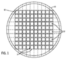
図1を参照すると、ウェーハ10が、複数のウェーハ・レベル・パッケージ(WLP)又はダイ12(すなわちウェーハ・スケール・パッケージ)に分割されているものとして示されている。ウェーハ10は一般的には、単結晶シリコン・インゴット又は多結晶シリコン・インゴットから切り出され、表面に集積回路のレイアウトが形成されるように準備される。ウェーハ10は上に形成されたICを有しており、複数のWLP12で構成されて、WLP12の各々の間にはウェーハ10を複数の個別のWLP12又はダイに切断するために確保されているダイス域14を含んでいる。
Referring to FIG. 1, a
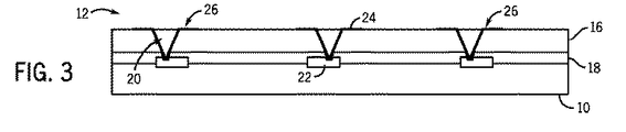
図2に示すように、WLP12を製造する際には、間に施工された接着剤材料18によって基材ポリマー・ラミネート層16をシリコン・ウェーハ10に施工する。基材ポリマー・ラミネート層16は、従来技術で用いられているような塗布手法によって形成/施工される層とは対照的に、シリコン・ウェーハ10の上に載置され得る予備形成されたラミネート・シート又はフィルムの形態にある。基材ポリマー・ラミネート16は、Kapton(商標)、Ultem(商標)、ポリテトラフルオロエチレン(PTFE)、又は液晶ポリマー(LCP)のような他のポリマー・フィルムで形成され得る。図3を参照して述べると、基材ポリマー・ラミネート層16のシリコン・ウェーハ10への施工後に、複数のバイア20がラミネート層に形成される。バイア20は、レーザ焼灼法又はレーザ穿孔法によって形成され、シリコン・ウェーハ10に配置されたダイ・パッド22に対応する位置に形成される。このようにして、基材ポリマー・ラミネート層16でのバイア20のレーザ穿孔によってダイ・パッド22が露出する。
As shown in FIG. 2, when the
バイア20の形成後に、金属層/材料24を、例えばスパッタリング法又は電気めっき法によって基材ポリマー・ラミネート層16に施工する。次いで、堆積した金属層/材料24を金属インタコネクト26として形成する。手法の一例では、基材ポリマー・ラミネート層16の上面28からバイア20を通って下降して延在する金属インタコネクト26が形成されるように、金属層/材料24をパターニングしてエッチングする。このようにして、金属インタコネクト26はダイ・パッド22との電気的接続を形成する。この態様で、基材ポリマー・ラミネート層16は、(例えば)各々のWLP12の周辺に配列され得るダイ・パッド22の構成を再配置してWLPの表面に配分されたインタコネクトの面積型アレイとするように作用する再配置層を形成する。このことについて以下に詳述する。
After the via 20 is formed, the metal layer /
図4には、ポリマー・ラミネート及び金属インタコネクト26を施工したシリコン・ウェーハ10の上面図が示されている。WLPの製造時、ポリマー・ラミネート層16のシリコン・ウェーハ10への積層の後に、ウェーハの残留応力を除去する/低下させるステップを実行する。すなわち、ポリマー・ラミネート層16の積層によってシリコン・ウェーハ10に加わり得る残留応力を減少させる又は除去するために、過剰なポリマー材料をWLP12の各々の間のダイス域14から除去する。ポリマー材料は、例えばレーザ焼灼法又はダイス鋸引き法によってダイス域14に複数の溝30(すなわち罫書き道(scribe street))を形成することにより除去される。溝30は100マイクロメートルの範囲にあってよい。溝30の形成は、後に行なわれる追加のポリマー再配置層の施工の後にシリコン・ウェーハ10に反り及び歪みが生じないようにするのに役立つ。
FIG. 4 shows a top view of the
図5に示すように、過剰なポリマー材料をダイス域から除去した後に、1又は複数の追加のポリマー・ラミネート層32を基材ポリマー・ラミネート層16に施工する。上で述べたステップと同様に、例えばレーザ焼灼法又はレーザ穿孔法によって追加のポリマー・ラミネート層32に複数のバイア20を形成する。追加のポリマー・ラミネート層32の各々のバイア20は、金属インタコネクト26のさらなる再配置を可能にするように、直下に配置されたポリマー・ラミネート層(例えば基材ポリマー・ラミネート層16)に取り付けられた金属インタコネクト26に対応する位置に形成される。次いで、上で詳細に述べたように、バイア20を通って下降して延在し、直下に配置されたポリマー・ラミネート層16の金属インタコネクト26と電気的に接触するように金属インタコネクト26を変形させるために、堆積(例えばスパッタリング又は電気めっき)法並びに続いて行なわれるパターニング及びエッチング法によって、追加のポリマー・ラミネート層32に金属インタコネクトを再び形成する。
As shown in FIG. 5, one or more additional polymer laminate layers 32 are applied to the substrate
続けて図5を参照して述べると、所望の数の追加のポリマー・ラミネート層32がシリコン・ウェーハ10に施工された後に、複数の入出力(I/O)インタコネクト34を最上のポリマー・ラミネート層の金属インタコネクト26に施工して、I/Oシステム・インタコネクト36を形成する。一実施形態では、I/Oインタコネクト34は、金属インタコネクト26に半田付けされたボール(すなわち半田ボール)として形成される。但し、WLP12とWLP12が取り付けられたマザー・ボード(図示されていない)との間に信頼性の高い接続が形成され得るように、めっきバンプ、柱状バンプ、金スタッド・バンプ、金属充填ポリマー・バンプ、又は結線接続/パッドのような他の形態のI/Oインタコネクト34を取り付けてもよい。
With continued reference to FIG. 5, after the desired number of additional polymer laminate layers 32 have been applied to the
複数のポリマー・ラミネート層16、32の逐次施工によって提供される金属インタコネクト26の再配置によって、増大した数のI/Oインタコネクト34をWLP12の上面に形成することが可能になる。すなわち、例えば、金属インタコネクト26の再配置によって、半田接続34をWLP12にさらに稠密に充填することができる。このように、WLP12の半田接続34は、従来の半田ボールに比較して減少したピッチ及び高さを有して形成される。例えば、半田接続34は、高さ180マイクロメートル及びピッチ80マイクロメートルを有するように形成され得る。可撓性のポリマー・ラミネート層におけるかかる寸法での半田接続34の形成によって、WLP12とWLP12が装着されたマザー・ボード(図示されていない)との間の接続接合応力が低下し、このようにして、従来技術において典型的に行なわれているようなWLPのマザー・ボードへの半田付けの後に行なわれる半田接続34とWLPとマザー・ボードとの間に施工されるアンダフィル・エポキシ混合物の必要性もなくす。
The repositioning of the
図5にさらに詳細に示すように、シリコン・ウェーハ10を、厚みを減らすように背面研磨し得ることも思量される。複数のポリマー・ラミネート層16、32は、背面研磨を実行するのに十分な強度を提供していなかった塗布層に比較してかかる背面研磨法のための十分な支持を与える。シリコン・ウェーハ10の背面研磨によって、WLP12の深さ/厚みを減らすことが可能になり、WLP12のさらなる小型化が可能になる。シリコン・ウェーハ10を所望の厚みに背面研磨した後に、図6に示すようにウェーハを複数の個別のWLP12に単独化するようにシリコン・ウェーハ10を切断することができる。
As shown in more detail in FIG. 5, it is contemplated that the
本発明の製造工程によって提供されるもう一つの有益な改良においては、一体化され得る付加的な要素によってWLP12にさらに大きい機能性を与え得ることが思量される。すなわち、WLP12を形成するためにシリコン・ウェーハ10に施工される複数の逐次的積層16、32は、WLP12におけるダイ・パッドの再配置を可能にするばかりでなく、複数の素子の一体化を可能にすることができる。図7を参照して述べると、一実施形態において、エア・ブリッジ及び/又は微小電気機械システム(MEMS)のような1又は複数の微小構造40を配置することを可能にするように、隣り合ったポリマー・ラミネート層16、32の間に空洞38を形成することができる。空洞38は、微小構造40に対する保護を提供し、このようにして寿命を延ばしてWLP12の信頼性を高める。
In another beneficial improvement provided by the manufacturing process of the present invention, it is envisioned that additional functionality that can be integrated can provide
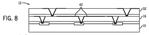
もう一つの実施形態では、図8に示すように、薄膜抵抗器、キャパシタ、又はインダクタのような埋め込み型受動素子42をWLP12に一体化してもよいことが認められよう。すなわち、埋め込み型受動素子42を別個の金属化工程時に隣接する(すなわち隣り合った)ポリマー・ラミネート層16、32の間に施工して、WLP12のさらなる機能性を提供することができる。さらにもう一つの実施形態として、図9は隣り合ったポリマー・ラミネート層16、32の間に金属製遮蔽要素44を含めることを示している。遮蔽要素44は、無線周波数(RF)又は電磁干渉(EMI)に対する遮蔽をWLP12に提供することができる。図7〜図9に示す微小電子素子の施工は、層16、32のシリコン・ウェーハ10への逐次積層によって可能となり、このようにして、かかる微小電子素子の一体化が可能でなかったシリコン・ウェーハへの層の従来の塗布施工と区別される。
It will be appreciated that in another embodiment, embedded
ここで図10を参照すると、同図には完成したWLP50が示されている。WLP50は、内部に複数の再配置層52を含むものとして示されている。3層の再配置層52を含むものとして図示されているが、例えばWLP50が5層又は6層の再配置層52を含むように付加的な層を施工し得ることが思量される。シリコン・ウェーハ56に含まれるダイ・パッド54からの接続を、再配置層52の各々を通して形成される複数の金属インタコネクト58によって再配線する。金属インタコネクト58が再配置層52のバイア60を通して形成されて、複数の再配置層52の各々を電気的に接続する。複数の半田接続62(例えば半田ボール)が、最上の再配置層52の金属インタコネクト58に施工される。複数の半田接続62は、WLP50の小型化及びWLPとマザー・ボード(図示されていない)との間の低応力接続を可能にした高密度インタコネクト(HDI)システム64を形成する。
Referring now to FIG. 10, the completed
限定された数の実施形態に関して本発明を詳細に説明したが、本発明はかかる開示された実施形態に限定されないことを容易に理解されよう。寧ろ、本発明は、本書には記載していないが本発明の真意及び範囲に添った任意の数の変形、変更、置換又は均等構成を組み入れるように改変され得るものである。加えて、本発明の様々な実施形態について記載したが、本発明の各観点は所載の実施形態の一部のみを包含する場合もあることを理解されたい。従って、本発明は、以上の記載によって限定されるものと解釈されるのではなく、特許請求の範囲によって限定されるものとする。 Although the invention has been described in detail with respect to a limited number of embodiments, it will be readily understood that the invention is not limited to such disclosed embodiments. Rather, the present invention may be modified to incorporate any number of variations, alterations, substitutions or equivalent arrangements not described herein but which are within the spirit and scope of the present invention. In addition, while various embodiments of the invention have been described, it should be understood that each aspect of the invention may encompass only some of the described embodiments. Accordingly, the invention is not to be construed as limited by the foregoing description, but is limited only by the scope of the claims.
従って、本発明の一実施形態によれば、ウェーハ・レベル・パッケージが、上面に形成された複数のダイ・パッドを有するシリコン集積回路(IC)基材と、このIC基材の上に配置され別個の予備形成されたラミネート・シートを含む複数のポリマー・ラミネートとを含んでおり、複数のポリマー・ラミネートの各々が、内部に形成された複数のバイアを有し、複数のバイアの各々がそれぞれのダイ・パッドに対応する。ウェーハ・レベル・パッケージはまた、複数のポリマー・ラミネートの各々の上に形成された複数の金属インタコネクトを含んでおり、複数の金属インタコネクトの各々が、それぞれのポリマー・ラミネートの上面の一部を被覆してバイアを通って下降して延在し、下方に配置された隣接したポリマー・ラミネートの金属インタコネクトと接触している。ウェーハ・レベル・パッケージはさらに、ウェーハ・レベル・パッケージの上面に配置されて複数の金属インタコネクトに取り付けられた入出力(I/O)システム・インタコネクトを含んでいる。 Thus, according to one embodiment of the present invention, a wafer level package is disposed on and over a silicon integrated circuit (IC) substrate having a plurality of die pads formed thereon. A plurality of polymer laminates including separate preformed laminate sheets, each of the plurality of polymer laminates having a plurality of vias formed therein, each of the plurality of vias being respectively It corresponds to the die pad. The wafer level package also includes a plurality of metal interconnects formed on each of the plurality of polymer laminates, each of the plurality of metal interconnects being part of the top surface of the respective polymer laminate. And extends down through the via and is in contact with the adjacent polymer laminate metal interconnect disposed below. The wafer level package further includes an input / output (I / O) system interconnect disposed on the top surface of the wafer level package and attached to a plurality of metal interconnects.
本発明のもう一つの実施形態によれば、ウェーハ・レベル・パッケージを形成する方法が、上面に集積回路(IC)を有すると共にICの上面に形成された複数のダイ・パッドを有するシリコン・ウェーハを設けるステップと、シリコン・ウェーハの上面に基材ポリマー・ラミネート層を接着するステップと、基材ポリマー・ラミネート層に複数のバイアを形成するステップとを含んでおり、複数のバイアの各々が、複数のダイ・パッドのそれぞれまで下降して延在している。この方法はまた、複数の金属インタコネクトの各々がそれぞれのバイアを通って下降して延在し、それぞれのダイ・パッドに電気的に接続するように、基材ポリマー・ラミネート層に複数の金属インタコネクトを形成するステップと、基材ポリマー・ラミネート層及び金属インタコネクトに少なくとも1層の追加のポリマー・ラミネート層を加えるステップとを含んでいる。この方法はさらに、最上のポリマー・ラミネート層の金属インタコネクトに複数の入出力(I/O)接続を取り付けるステップと、シリコン・ウェーハを複数のウェーハ・レベル・パッケージまで単独化させるステップとを含んでおり、各々のウェーハ・レベル・パッケージが、複数の金属インタコネクトの部分及びその上に複数のI/O接続の部分を含んでいる。 In accordance with another embodiment of the present invention, a method of forming a wafer level package includes a silicon wafer having an integrated circuit (IC) on a top surface and a plurality of die pads formed on the top surface of the IC. Providing a base polymer laminate layer on the top surface of the silicon wafer, and forming a plurality of vias in the base polymer laminate layer, each of the plurality of vias comprising: Extending down to each of the plurality of die pads. The method also includes a plurality of metals in the substrate polymer laminate layer such that each of the plurality of metal interconnects extends down through the respective via and is electrically connected to the respective die pad. Forming an interconnect and adding at least one additional polymer laminate layer to the base polymer laminate layer and the metal interconnect. The method further includes attaching a plurality of input / output (I / O) connections to the metal interconnect of the uppermost polymer laminate layer and isolating the silicon wafer to a plurality of wafer level packages. Each wafer level package includes a plurality of metal interconnect portions and a plurality of I / O connection portions thereon.
本発明のさらにもう一つの実施形態によれば、ウェーハ・レベル・パッケージを製造する方法が、上面に形成された複数のダイ・パッドを有するシリコン・ウェーハを設けるステップと、シリコン・ウェーハの上面に複数の再配置層を逐次積層するステップとを含んでおり、複数の再配置層の各々が複数の金属インタコネクトを内部に有している。この方法はまた、複数の入出力(I/O)インタコネクト・システムを最上の再配置層の金属インタコネクトに取り付けるステップと、シリコン・ウェーハを複数のウェーハ・レベル・パッケージに単独化するステップとを含んでおり、各々のウェーハ・レベル・パッケージが、複数の金属インタコネクトの部分集合及びその上に複数のI/O接続の部分集合を含んでいる。 According to yet another embodiment of the present invention, a method of manufacturing a wafer level package includes providing a silicon wafer having a plurality of die pads formed on a top surface, and forming a top surface on the silicon wafer. Sequentially stacking a plurality of relocation layers, each of the plurality of relocation layers having a plurality of metal interconnects therein. The method also includes attaching a plurality of input / output (I / O) interconnect systems to the top redistribution layer metal interconnect, and singulating the silicon wafer into a plurality of wafer level packages. Each wafer level package includes a plurality of metal interconnect subsets and a plurality of I / O connection subsets thereon.
新規であり特許証による保護を求めるものとして請求される内容を以下に添付する。 What is claimed as new and seeks protection by patent is attached below.
10 ウェーハ
12 ダイ
14 ダイス域
16 基材ポリマー・ラミネート層
18 接着剤材料
20 バイア
22 ダイ・パッド
24 金属層/材料
26 金属インタコネクト
28 上面
30 溝
32 追加のポリマー・ラミネート層
34 入出力(I/O)インタコネクト
36 I/Oシステム・インタコネクト
38 空洞
40 微小構造
42 埋め込み型受動素子
44 遮蔽要素
50 完成したWLP
52 再配置層
54 ダイ・パッド
56 シリコン・ウェーハ
58 金属インタコネクト
60 バイア
62 半田接続
64 高密度インタコネクト(HDI)システム
10
52
Claims (10)
該IC基材(10)の上に配置された複数のポリマー・ラミネート(16)であって、当該複数のポリマー・ラミネート(16)の各々が、内部に形成された複数のバイア(20)を有し、該複数のバイア(20)の各々がそれぞれのダイ・パッド(22)に対応している、複数のポリマー・ラミネート(16)と、
該複数のポリマー・ラミネート(16)の各々に形成された複数のインタコネクト(26)であって、当該複数のインタコネクト(26)の各々がそれぞれのポリマー・ラミネート(16)の上面の一部を被覆して前記バイア(20)を通って下降して延在し、下方に配置された隣接したポリマー・ラミネート(16)のインタコネクト(26)と接触している、複数のインタコネクト(26)と、
当該ウェーハ・レベル・パッケージ(12)の上面に配置されて前記複数の金属インタコネクト(26)に取り付けられた入出力(I/O)システム・インタコネクト(34)と、
を備えたウェーハ・レベル・パッケージ(12)であって、
前記複数のポリマー・ラミネート(16)の各々が、別個の予備形成されたラミネート・シートを含んでおり、
前記複数のポリマー・ラミネート(16)のそれぞれは、ダイス域を含み、
前記ダイス域は、ポリマー材料の少なくとも一部が除去されることにより形成された、前記IC基材(10)の残留応力を減少させる複数の溝を有しており、
前記複数の溝(30)が形成された前記複数のポリマー・ラミネート層及び前記インタコネクトに積層された少なくとも1層の追加のポリマー・ラミネート層をさらに含む、
ウェーハ・レベル・パッケージ(12)。 An integrated circuit (IC) substrate (10) having a plurality of die pads (22) formed on an upper surface;
A plurality of polymer laminates (16) disposed on the IC substrate (10), each of the plurality of polymer laminates (16) having a plurality of vias (20) formed therein. A plurality of polymer laminates (16), each of the plurality of vias (20) corresponding to a respective die pad (22);
A plurality of interconnects (26) formed in each of the plurality of polymer laminates (16), wherein each of the plurality of interconnects (26) is a portion of the top surface of the respective polymer laminate (16). A plurality of interconnects (26) extending down through the vias (20) and in contact with interconnects (26) of adjacent polymer laminates (16) disposed below )When,
An input / output (I / O) system interconnect (34) disposed on an upper surface of the wafer level package (12) and attached to the plurality of metal interconnects (26);
A wafer level package (12) comprising:
Each of the plurality of polymer laminates (16) comprises a separate preformed laminate sheet;
Each of the plurality of polymer laminates (16) includes a die area;
The die region has a plurality of grooves formed by removing at least a part of a polymer material and reducing a residual stress of the IC substrate (10);
And further comprising at least one additional polymer laminate layer laminated to the interconnect and the plurality of polymer laminate layers formed with the plurality of grooves (30).
Wafer level package (12).
前記ウェーハ・レベル・パッケージ(12)を形成するように、前記複数のポリマー・ラミネート(16)の各々の外形が、前記ダイ(12)の寸法とほぼ同じである、請求項1乃至5のいずれかに記載のウェーハ・レベル・パッケージ(12)。 The IC substrate (10) comprises a die (12) having a plurality of die pads on its upper surface,
6. Any one of claims 1 to 5 , wherein the outer shape of each of the plurality of polymer laminates (16) is substantially the same as the dimensions of the die (12) so as to form the wafer level package (12). A wafer level package (12) according to the above.
上面に集積回路(IC)を有すると共に前記ICの上面に形成された複数のダイ・パッドを有するシリコン・ウェーハを設けるステップと、
前記シリコン・ウェーハの上面に基材ポリマー・ラミネート層を接着するステップと、
前記基材ポリマー・ラミネート層に複数のバイアを形成するステップであって、前記複数のバイアの各々が、前記複数のダイ・パッドのそれぞれまで下降して延在している、前記ステップと、
複数のインタコネクトの各々がそれぞれのバイアを通って下降して延在し、それぞれのダイ・パッドに電気的に接続するように、基材ポリマー・ラミネート層に前記複数のインタコネクトを形成するステップと、
前記基材ポリマー・ラミネート層に複数の溝(30)を形成して、前記ウェーハ)の残留応力を減少させるステップと、
前記複数の溝(30)が形成された前記基材ポリマー・ラミネート層及び前記インタコネクトに少なくとも1層の追加のポリマー・ラミネート層を加えるステップと、
最上のポリマー・ラミネート層のインタコネクトに複数の入出力(I/O)接続を取り付けるステップと、
を含み、
各々のウェーハ・レベル・パッケージが、複数のインタコネクトの部分及びその上に複数のI/O接続の部分を含んでおり、
前記複数の溝は、前記複数のウェーハ・レベル・パッケージの間のダイ領域に形成され、前記少なくとも1層の追加のポリマー・ラミネート層を加える前に各ポリマー・ラミネート層に形成される、
方法。 A method of forming a wafer level package comprising:
Providing a silicon wafer having an integrated circuit (IC) on the top surface and having a plurality of die pads formed on the top surface of the IC;
Adhering a base polymer laminate layer to the top surface of the silicon wafer;
Forming a plurality of vias in the base polymer laminate layer, each of the plurality of vias extending down to each of the plurality of die pads; and
Forming the plurality of interconnects in the base polymer laminate layer such that each of the plurality of interconnects extends downwardly through the respective via and electrically connects to the respective die pad. When,
Forming a plurality of grooves (30) in the base polymer laminate layer to reduce residual stress of the wafer);
Adding at least one additional polymer laminate layer to the substrate polymer laminate layer and the interconnect in which the plurality of grooves (30) are formed;
Attaching multiple input / output (I / O) connections to the top polymer laminate layer interconnect;
Including
Each wafer level package includes a plurality of interconnect portions and a plurality of I / O connection portions thereon,
The plurality of grooves are formed in a die region between the plurality of wafer level packages and formed in each polymer laminate layer prior to adding the at least one additional polymer laminate layer.
Method.
前記シリコン・ウェーハを切断して複数のウェーハ・レベル・パッケージ(12)を形成するステップと、
を含んでいる請求項7乃至9のいずれかに記載の方法。
Backside polishing the silicon wafer to reduce its thickness after adding the at least one additional polymer laminate layer;
Cutting the silicon wafer to form a plurality of wafer level packages (12);
10. A method according to any one of claims 7 to 9 comprising:
Applications Claiming Priority (2)
| Application Number | Priority Date | Filing Date | Title |
|---|---|---|---|
| US12/059,075 US7952187B2 (en) | 2008-03-31 | 2008-03-31 | System and method of forming a wafer scale package |
| US12/059,075 | 2008-03-31 |
Publications (3)
| Publication Number | Publication Date |
|---|---|
| JP2009246367A JP2009246367A (en) | 2009-10-22 |
| JP2009246367A5 JP2009246367A5 (en) | 2012-05-17 |
| JP5588620B2 true JP5588620B2 (en) | 2014-09-10 |
Family
ID=40809871
Family Applications (1)
| Application Number | Title | Priority Date | Filing Date |
|---|---|---|---|
| JP2009081073A Active JP5588620B2 (en) | 2008-03-31 | 2009-03-30 | Wafer level package and method of forming the same |
Country Status (5)
| Country | Link |
|---|---|
| US (1) | US7952187B2 (en) |
| EP (1) | EP2107599B1 (en) |
| JP (1) | JP5588620B2 (en) |
| KR (1) | KR101568043B1 (en) |
| TW (1) | TWI492318B (en) |
Families Citing this family (11)
| Publication number | Priority date | Publication date | Assignee | Title |
|---|---|---|---|---|
| US8114708B2 (en) * | 2008-09-30 | 2012-02-14 | General Electric Company | System and method for pre-patterned embedded chip build-up |
| US10276486B2 (en) | 2010-03-02 | 2019-04-30 | General Electric Company | Stress resistant micro-via structure for flexible circuits |
| TWI421957B (en) * | 2010-08-04 | 2014-01-01 | Universal Scient Ind Shanghai | Manufacturing method for system in package and package structure thereof |
| US8829676B2 (en) * | 2011-06-28 | 2014-09-09 | Taiwan Semiconductor Manufacturing Company, Ltd. | Interconnect structure for wafer level package |
| US8824161B2 (en) | 2012-06-15 | 2014-09-02 | Medtronic, Inc. | Integrated circuit packaging for implantable medical devices |
| US9368460B2 (en) | 2013-03-15 | 2016-06-14 | Taiwan Semiconductor Manufacturing Company, Ltd. | Fan-out interconnect structure and method for forming same |
| US9484318B2 (en) * | 2014-02-17 | 2016-11-01 | Taiwan Semiconductor Manufacturing Company Ltd. | Semiconductor device and manufacturing method thereof |
| US10432168B2 (en) | 2015-08-31 | 2019-10-01 | General Electric Company | Systems and methods for quartz wafer bonding |
| US10333493B2 (en) * | 2016-08-25 | 2019-06-25 | General Electric Company | Embedded RF filter package structure and method of manufacturing thereof |
| KR102385549B1 (en) | 2017-08-16 | 2022-04-12 | 삼성전자주식회사 | Semiconductor package and method of manufacturing the semiconductor package |
| US20190206786A1 (en) * | 2017-12-28 | 2019-07-04 | Intel Corporation | Thin film passive devices integrated in a package substrate |
Family Cites Families (17)
| Publication number | Priority date | Publication date | Assignee | Title |
|---|---|---|---|---|
| US5366906A (en) | 1992-10-16 | 1994-11-22 | Martin Marietta Corporation | Wafer level integration and testing |
| US5561085A (en) * | 1994-12-19 | 1996-10-01 | Martin Marietta Corporation | Structure for protecting air bridges on semiconductor chips from damage |
| EP0734059B1 (en) * | 1995-03-24 | 2005-11-09 | Shinko Electric Industries Co., Ltd. | Chip sized semiconductor device and a process for making it |
| US6773962B2 (en) * | 2001-03-15 | 2004-08-10 | General Electric Company | Microelectromechanical system device packaging method |
| US6673698B1 (en) * | 2002-01-19 | 2004-01-06 | Megic Corporation | Thin film semiconductor package utilizing a glass substrate with composite polymer/metal interconnect layers |
| JP3951788B2 (en) * | 2002-04-25 | 2007-08-01 | 株式会社デンソー | Surface mount electronic components |
| JP3972246B2 (en) * | 2003-01-07 | 2007-09-05 | ソニー株式会社 | Wafer level chip size package and manufacturing method thereof |
| JP4285079B2 (en) * | 2003-05-22 | 2009-06-24 | カシオ計算機株式会社 | Manufacturing method of semiconductor device |
| KR100609011B1 (en) * | 2003-12-05 | 2006-08-03 | 삼성전자주식회사 | Wafer level module and fabricating method thereof |
| JP2005268297A (en) * | 2004-03-16 | 2005-09-29 | Hitachi Media Electoronics Co Ltd | High frequency device and its fabrication method |
| US7189594B2 (en) * | 2004-09-10 | 2007-03-13 | Agency For Science, Technology And Research | Wafer level packages and methods of fabrication |
| JP3976043B2 (en) * | 2004-10-25 | 2007-09-12 | セイコーエプソン株式会社 | Semiconductor device and manufacturing method thereof |
| JP4774248B2 (en) * | 2005-07-22 | 2011-09-14 | Okiセミコンダクタ株式会社 | Semiconductor device |
| JP4193897B2 (en) * | 2006-05-19 | 2008-12-10 | カシオ計算機株式会社 | Semiconductor device and manufacturing method thereof |
| DE102006032431B4 (en) * | 2006-06-22 | 2011-12-01 | Siltronic Ag | Method and device for detecting mechanical defects in a rod made of semiconductor material |
| US7626269B2 (en) * | 2006-07-06 | 2009-12-01 | Micron Technology, Inc. | Semiconductor constructions and assemblies, and electronic systems |
| JP4679553B2 (en) * | 2007-07-23 | 2011-04-27 | イビデン株式会社 | Semiconductor chip |
-
2008
- 2008-03-31 US US12/059,075 patent/US7952187B2/en active Active
-
2009
- 2009-03-18 TW TW098108766A patent/TWI492318B/en active
- 2009-03-26 EP EP09156243.9A patent/EP2107599B1/en active Active
- 2009-03-30 KR KR1020090027087A patent/KR101568043B1/en active IP Right Grant
- 2009-03-30 JP JP2009081073A patent/JP5588620B2/en active Active
Also Published As
| Publication number | Publication date |
|---|---|
| KR101568043B1 (en) | 2015-11-10 |
| KR20090104744A (en) | 2009-10-06 |
| JP2009246367A (en) | 2009-10-22 |
| EP2107599A2 (en) | 2009-10-07 |
| US7952187B2 (en) | 2011-05-31 |
| EP2107599A3 (en) | 2012-11-21 |
| TWI492318B (en) | 2015-07-11 |
| EP2107599B1 (en) | 2019-07-03 |
| US20090243081A1 (en) | 2009-10-01 |
| TW201001577A (en) | 2010-01-01 |
Similar Documents
| Publication | Publication Date | Title |
|---|---|---|
| JP5588620B2 (en) | Wafer level package and method of forming the same | |
| JP5639368B2 (en) | System and method for stacked die embedded chip build-up | |
| TWI597788B (en) | Semiconductor device and manufacturing method thereof | |
| US9368474B2 (en) | Manufacturing method for semiconductor device | |
| US20180342414A1 (en) | Wafer Level Chip Scale Packaging Intermediate Structure Apparatus and Method | |
| US9236348B2 (en) | Ultrathin buried die module and method of manufacturing thereof | |
| TWI536519B (en) | Semiconductor package structure and manufacturing method thereof | |
| JP5942823B2 (en) | Electronic component device manufacturing method, electronic component device, and electronic device | |
| US8114708B2 (en) | System and method for pre-patterned embedded chip build-up | |
| KR101157726B1 (en) | Ultra-thin stacked chips packaging | |
| US10121736B2 (en) | Method of fabricating packaging layer of fan-out chip package | |
| CN110970312B (en) | Package and method of forming the same | |
| KR20140107129A (en) | Semiconductor device and method for manufacturing semiconductor device | |
| CN107068625B (en) | Polymer-based semiconductor structure with cavity | |
| US20090085190A1 (en) | Semiconductor Device and Method for Making Same | |
| CN113539844A (en) | Semiconductor device and method for manufacturing the same | |
| JP2005005632A (en) | Chip-like electronic component, its manufacturing method, and its packaging structure | |
| US8680683B1 (en) | Wafer level package with embedded passive components and method of manufacturing | |
| JP2004319656A (en) | Method of manufacturing wafer level csp | |
| WO2010043657A1 (en) | Electronic component and method of manufacturing the same |
Legal Events
| Date | Code | Title | Description |
|---|---|---|---|
| A521 | Request for written amendment filed |
Free format text: JAPANESE INTERMEDIATE CODE: A523 Effective date: 20120321 |
|
| A621 | Written request for application examination |
Free format text: JAPANESE INTERMEDIATE CODE: A621 Effective date: 20120321 |
|
| A521 | Request for written amendment filed |
Free format text: JAPANESE INTERMEDIATE CODE: A523 Effective date: 20130313 |
|
| A977 | Report on retrieval |
Free format text: JAPANESE INTERMEDIATE CODE: A971007 Effective date: 20130628 |
|
| A131 | Notification of reasons for refusal |
Free format text: JAPANESE INTERMEDIATE CODE: A131 Effective date: 20130702 |
|
| A521 | Request for written amendment filed |
Free format text: JAPANESE INTERMEDIATE CODE: A523 Effective date: 20130819 |
|
| A131 | Notification of reasons for refusal |
Free format text: JAPANESE INTERMEDIATE CODE: A131 Effective date: 20140520 |
|
| A521 | Request for written amendment filed |
Free format text: JAPANESE INTERMEDIATE CODE: A523 Effective date: 20140617 |
|
| TRDD | Decision of grant or rejection written | ||
| A01 | Written decision to grant a patent or to grant a registration (utility model) |
Free format text: JAPANESE INTERMEDIATE CODE: A01 Effective date: 20140709 |
|
| A61 | First payment of annual fees (during grant procedure) |
Free format text: JAPANESE INTERMEDIATE CODE: A61 Effective date: 20140728 |
|
| R150 | Certificate of patent or registration of utility model |
Ref document number: 5588620 Country of ref document: JP Free format text: JAPANESE INTERMEDIATE CODE: R150 |
|
| R250 | Receipt of annual fees |
Free format text: JAPANESE INTERMEDIATE CODE: R250 |
|
| R250 | Receipt of annual fees |
Free format text: JAPANESE INTERMEDIATE CODE: R250 |
|
| R250 | Receipt of annual fees |
Free format text: JAPANESE INTERMEDIATE CODE: R250 |
|
| R250 | Receipt of annual fees |
Free format text: JAPANESE INTERMEDIATE CODE: R250 |
|
| R250 | Receipt of annual fees |
Free format text: JAPANESE INTERMEDIATE CODE: R250 |
|
| R250 | Receipt of annual fees |
Free format text: JAPANESE INTERMEDIATE CODE: R250 |
|
| R250 | Receipt of annual fees |
Free format text: JAPANESE INTERMEDIATE CODE: R250 |