JP5586054B2 - Microphone connector - Google Patents
Microphone connector Download PDFInfo
- Publication number
- JP5586054B2 JP5586054B2 JP2010190292A JP2010190292A JP5586054B2 JP 5586054 B2 JP5586054 B2 JP 5586054B2 JP 2010190292 A JP2010190292 A JP 2010190292A JP 2010190292 A JP2010190292 A JP 2010190292A JP 5586054 B2 JP5586054 B2 JP 5586054B2
- Authority
- JP
- Japan
- Prior art keywords
- pin
- shield
- shield cover
- connector
- circuit board
- Prior art date
- Legal status (The legal status is an assumption and is not a legal conclusion. Google has not performed a legal analysis and makes no representation as to the accuracy of the status listed.)
- Expired - Fee Related
Links
Images


Classifications
-
- H—ELECTRICITY
- H01—ELECTRIC ELEMENTS
- H01R—ELECTRICALLY-CONDUCTIVE CONNECTIONS; STRUCTURAL ASSOCIATIONS OF A PLURALITY OF MUTUALLY-INSULATED ELECTRICAL CONNECTING ELEMENTS; COUPLING DEVICES; CURRENT COLLECTORS
- H01R13/00—Details of coupling devices of the kinds covered by groups H01R12/70 or H01R24/00 - H01R33/00
- H01R13/66—Structural association with built-in electrical component
- H01R13/665—Structural association with built-in electrical component with built-in electronic circuit
- H01R13/6658—Structural association with built-in electrical component with built-in electronic circuit on printed circuit board
-
- H—ELECTRICITY
- H01—ELECTRIC ELEMENTS
- H01R—ELECTRICALLY-CONDUCTIVE CONNECTIONS; STRUCTURAL ASSOCIATIONS OF A PLURALITY OF MUTUALLY-INSULATED ELECTRICAL CONNECTING ELEMENTS; COUPLING DEVICES; CURRENT COLLECTORS
- H01R13/00—Details of coupling devices of the kinds covered by groups H01R12/70 or H01R24/00 - H01R33/00
- H01R13/66—Structural association with built-in electrical component
- H01R13/719—Structural association with built-in electrical component specially adapted for high frequency, e.g. with filters
- H01R13/7195—Structural association with built-in electrical component specially adapted for high frequency, e.g. with filters with planar filters with openings for contacts
-
- H—ELECTRICITY
- H01—ELECTRIC ELEMENTS
- H01R—ELECTRICALLY-CONDUCTIVE CONNECTIONS; STRUCTURAL ASSOCIATIONS OF A PLURALITY OF MUTUALLY-INSULATED ELECTRICAL CONNECTING ELEMENTS; COUPLING DEVICES; CURRENT COLLECTORS
- H01R13/00—Details of coupling devices of the kinds covered by groups H01R12/70 or H01R24/00 - H01R33/00
- H01R13/46—Bases; Cases
- H01R13/502—Bases; Cases composed of different pieces
- H01R13/512—Bases; Cases composed of different pieces assembled by screw or screws
-
- H—ELECTRICITY
- H01—ELECTRIC ELEMENTS
- H01R—ELECTRICALLY-CONDUCTIVE CONNECTIONS; STRUCTURAL ASSOCIATIONS OF A PLURALITY OF MUTUALLY-INSULATED ELECTRICAL CONNECTING ELEMENTS; COUPLING DEVICES; CURRENT COLLECTORS
- H01R13/00—Details of coupling devices of the kinds covered by groups H01R12/70 or H01R24/00 - H01R33/00
- H01R13/648—Protective earth or shield arrangements on coupling devices, e.g. anti-static shielding
- H01R13/658—High frequency shielding arrangements, e.g. against EMI [Electro-Magnetic Interference] or EMP [Electro-Magnetic Pulse]
- H01R13/6591—Specific features or arrangements of connection of shield to conductive members
- H01R13/6597—Specific features or arrangements of connection of shield to conductive members the conductive member being a contact of the connector
-
- H—ELECTRICITY
- H01—ELECTRIC ELEMENTS
- H01R—ELECTRICALLY-CONDUCTIVE CONNECTIONS; STRUCTURAL ASSOCIATIONS OF A PLURALITY OF MUTUALLY-INSULATED ELECTRICAL CONNECTING ELEMENTS; COUPLING DEVICES; CURRENT COLLECTORS
- H01R2103/00—Two poles
-
- H—ELECTRICITY
- H01—ELECTRIC ELEMENTS
- H01R—ELECTRICALLY-CONDUCTIVE CONNECTIONS; STRUCTURAL ASSOCIATIONS OF A PLURALITY OF MUTUALLY-INSULATED ELECTRICAL CONNECTING ELEMENTS; COUPLING DEVICES; CURRENT COLLECTORS
- H01R24/00—Two-part coupling devices, or either of their cooperating parts, characterised by their overall structure
- H01R24/28—Coupling parts carrying pins, blades or analogous contacts and secured only to wire or cable
- H01R24/30—Coupling parts carrying pins, blades or analogous contacts and secured only to wire or cable with additional earth or shield contacts
Description
本発明は、マイクロホンのコネクタに関し、より詳しくは、ケーブルを伝播してマイクロホンに高周波電流が入り込むことを防止するマイクロホンのコネクタに関するものである。 The present invention relates to a microphone connector, and more particularly to a microphone connector that prevents a high-frequency current from entering a microphone by propagating a cable.
コンデンサマイクロホンは、そのマイクロホンユニットのインピーダンスがきわめて高いため、FET(電界効果トランジタ)などのインピーダンス変換器を内蔵している。通常、コンデンサマイクロホンにおいてはファントム電源が用いられ、マイク音声信号はファントム電源用の平衡シールドケーブルを介して出力される。平衡シールドケーブルを接続するため、マイクケース(手持ち式マイクロホンにおいてはマイクグリップ)側には3ピンタイプのコネクタが設けられる。通常用いられているコネクタはEIAJ RC−5236「音響機器用ラッチロック式丸形コネクタ」に規定されているコネクタである。 The condenser microphone has a built-in impedance converter such as a FET (field effect transistor) because the impedance of the microphone unit is extremely high. Normally, a phantom power supply is used in a condenser microphone, and a microphone sound signal is output via a balanced shield cable for the phantom power supply. In order to connect a balanced shielded cable, a 3-pin type connector is provided on the side of the microphone case (microphone grip in a handheld microphone). A connector that is normally used is a connector defined in EIAJ RC-5236 “Latch Lock Type Circular Connector for Acoustic Equipment”.
上記コネクタはPBT(ポリブタジエンテレフタレート)樹脂などの電気絶縁体からなる円盤状のコネクタ基台を備えている。コネクタ基台には3本のピン、すなわち接地用の1番ピン、信号のホット側の2番ピンおよび信号のコールド側の3番ピンが貫設されている。例えば手持ち式マイクロホンについて言えば、コネクタはマイクグリップの端部にねじ止めされるコネクタ収納筒内に装着される。通常、コネクタ収納筒を含めてマイクグリップは真鍮などの金属材からなり、内蔵される電気部品のシールドケースとしても作用する。コネクタ基台内には接地用の1番ピンをコネクタ収納筒に電気的に接続するための雄ねじが設けられている。 The connector includes a disk-shaped connector base made of an electrical insulator such as PBT (polybutadiene terephthalate) resin. The connector base is provided with three pins, namely, a first pin for grounding, a second pin on the hot side of the signal, and a third pin on the cold side of the signal. For example, in the case of a handheld microphone, the connector is mounted in a connector housing cylinder that is screwed to the end of the microphone grip. Normally, the microphone grip including the connector housing cylinder is made of a metal material such as brass, and also acts as a shield case for the built-in electrical parts. A male screw for electrically connecting the first pin for grounding to the connector housing cylinder is provided in the connector base.
このようなコネクタは、ファントム電源側から引き出されているマイクケーブル(平衡シールドケーブル)が接続された状態において、強い電磁波がマイクロホンやマイクケーブルに当たると、その電磁波がコネクタからマイクロホンの内部に入り込み、インピーダンス変換器で復調され可聴周波数の雑音としてマイクロホンから出力されてしまうことがある。 In such a connector, when a microphone cable (balanced shielded cable) drawn from the phantom power supply side is connected, when a strong electromagnetic wave hits the microphone or the microphone cable, the electromagnetic wave enters the microphone from the connector, and impedance The signal may be demodulated by the converter and output from the microphone as audible noise.
そこで、コネクタ基台の少なくとも一端面および周面が、各信号ピンと非導通で接地ピンと導通し、シールドカバーにて覆われているマイクロホンのコネクタが提案されている(例えば、特許文献1参照。)。 Therefore, a microphone connector is proposed in which at least one end surface and a peripheral surface of the connector base are not electrically connected to each signal pin but electrically connected to the ground pin, and are covered with a shield cover (see, for example, Patent Document 1). .
また、特許文献2では、3本のピンを挿通してコネクタ基台の一方の面に配置されるプリント配線板と、その3本のピンを挿通してプリント配線板とコネクタ基台を覆うように配置されるシールドカバーとを有しているマイクロホンのコネクタが開示されている。特許文献2に記載の発明では、プリント配線板に高周波侵入阻止用のコンデンサ素子と静電気による回路破壊防止用のツェナーダイオード素子が実装されており、プリント配線板のコンデンサ素子とツェナーダイオード素子の配置面側がシールドカバーで覆われている。上記各特許文献には、上述のようにすることにより、コネクタからマイクロホン本体への高周波電流の流入を防ぐことができると記載されている。
Further, in
近年の携帯電話機などの普及によってより高い周波数の電磁波がマイクロホンの近傍で使用される機会が増え、電磁波を原因とする雑音の発生が問題になっている。しかしながら、上記各特許文献に記載の発明では、マイクロホン近傍で放射される電磁波を原因とする雑音対策が十分ではなく、そのためシールドケースの電気的接続を確実にするための応力の強化が求められる。また、特許文献2に記載の発明においても、プリント基板の接地パターンと、シールドケースの電気的接続は、シールドケースとピンを機械的に結合するだけであるため、高い周波数の電磁波に対するシールド効果が十分とは言えない。
With the recent spread of mobile phones and the like, there is an increased chance that electromagnetic waves with higher frequencies are used in the vicinity of microphones, and the generation of noise due to electromagnetic waves has become a problem. However, in the inventions described in the above patent documents, countermeasures against noise caused by electromagnetic waves radiated in the vicinity of the microphone are not sufficient, and therefore, strengthening of stress is required to ensure electrical connection of the shield case. Also in the invention described in
本発明は、シールドケースとプリント基板の接地パターンとの電気的接続を確実にし、携帯電話機などで使用される高い周波数の電磁波に対するシールド効果を高めることができ、マイクロホン内部に高周波が輻射されることを防止することができるマイクロホンのコネクタの提供を目的とする。 The present invention ensures electrical connection between the shield case and the ground pattern of the printed circuit board, can enhance the shielding effect against high-frequency electromagnetic waves used in mobile phones and the like, and high-frequency radiation is radiated inside the microphone. An object of the present invention is to provide a microphone connector that can prevent the above-described problem.
本発明は、電気絶縁体からなるコネクタ基台に接地用の1番ピン、信号用の2番ピンおよび3番ピンで構成される3本のピンが貫設されてなる3ピンタイプのマイクロホンコネクタ、であって、上記3本のピンが挿通されて配置されているプリント基板と、上記プリント基板の上記コネクタ基台と対向する面には、上記2番ピン、3番ピンに対しては非導通で上記1番ピンとは導通するシールド層がほぼ全面にわたって形成されており、上記3本のピンが挿通されて上記プリント基板と上記コネクタ基台とを一方の面側から覆って配置される第1のシールドカバーと、上記3本のピンが挿通されて上記コネクタ基台を他方の面側から覆って配置されている第2のシールドカバーと、を有し、上記第1のシールドカバーは、有底円筒形であって、底部近傍の直径を小さくした肩部が設けられていて、上記第2のシールドカバーは、上記第1のシールドカバーの開放端部を塞ぐ円板状であり、上記プリント基板の上記一方の面側の周縁部には、上記プリント基板の他面側の上記シールド層とスルーホール内配線で導通されたシールド電極が形成されており、上記第1のシールドカバーと上記第2のシールドカバーは、互いの端部を押圧し合い、上記シールド電極が前記肩部と面的に接触して上記コネクタ基台を内包し、上記シールド電極と導通する、ことを最も主要な特徴とする。
The present invention provides a three-pin type microphone connector in which a connector base made of an electrical insulator is provided with three pins each including a first pin for grounding, a second pin for signals, and a third pin. , a, and a printed substrate on which the three pins are arranged is inserted, to the connector base and the opposing surfaces of the printed circuit board, the
本発明によれば、第1のシールドカバーと第2のシールドカバーは、互いの端部を押圧し合いコネクタ基台を内包していることで、シールドカバーとプリント基板の接地パターンに押圧力が充分に加わり、この部分の電気的接続が確実になり、コネクタの部品全体を囲むように静電シールドが構成され、マイクロホン内部に高周波が輻射されることを防止することができるマイクロホンのコネクタを提供することができる。 According to the present invention, the first shield cover and the second shield cover are pressed against each other and contain the connector base so that the pressing force is applied to the ground pattern of the shield cover and the printed circuit board. Provides a microphone connector that can sufficiently prevent electrical radiation from being radiated into the microphone, with an electrostatic shield constructed so that the electrical connection of this part is ensured and the entire parts of the connector are enclosed. can do.
以下、図1ないし図3により本発明の実施形態について説明する。 Hereinafter, an embodiment of the present invention will be described with reference to FIGS.
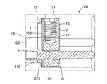
図1において、コネクタ10は、その主要な構成として円柱状の電気絶縁体からなるコネクタ基台11と、コネクタ基台11の一面側に重ねられて配置されているプリント基板100と、プリント基板100を覆う有底円筒形の第1のシールドカバー1と、円盤状の第2のシールドカバー2と、接地用の1番ピンE、信号のホット側の図示しない2番ピンSHおよび信号のコールド側の3番ピンSCの3本のピンを備えている。上記3本のピンは、第1のシールドカバー1、プリント基板100、コネクタ基台11、第2のシールドカバー2をこの順番で貫通している。
In FIG. 1, a
円筒状の第1のシールドカバー1は、上述の3本のピンが挿通されて、プリント基板100と、コネクタ基台11の周面とを、プリント基板100側の面から覆って配置されている。また、円盤状の第2のシールドカバー2は、上述の3本のピンが挿通されてコネクタ基台11をプリント基板100と逆側の面から覆って配置されている。第1のシールドカバー1と第2のシールドカバー2は、第1のシールドカバー1の開放端部がコネクタ基台11の外周縁部を抱き込むようにして半径方向内側に向かってかしめられることによって、符号Aで示すように互いの端部を押圧し合い、コネクタ基台11を内包している。なお、第2のシールドカバー2の端部を第1のシールドカバー1の端部側にかしめて互いの端部を押圧し合うようにし、コネクタ基台11を内包するようにすることもできる。
The
図1のように、コネクタ10は、マイクグリップの端部にねじ止めされるコネクタ収納筒20内に装着されている。コネクタ収納筒20を含めてマイクグリップは真鍮などの金属材からなり、内蔵される電気部品のシールドケースとしても作用する。コネクタ収納筒20には、適宜のドライバーなどで、雄ねじ13を引き出すための孔21が設けられている。上記雄ねじ13はコネクタ基台11の外周面から半径方向に向かって形成されたねじ孔12にねじ込まれている。雄ねじ13の頭部は小径に形成されて段状の肩部が形成されている。雄ねじ13の小径の頭部は、コネクタ収納筒20の上記孔21の径とほぼ同じ形になっていて上記孔21に嵌ることができ、雄ねじ13の上記肩部は上記孔21の周縁部に当たるようになっている。したがって、ねじ孔12から雄ねじ13を引き出すと、雄ねじ13の上記肩部がコネクタ収納筒20の上記孔21の周縁部に当たり、第1のシールドカバー1と第2のシールドカバー2で内包されたコネクタ基台11を、上記孔21の反対側に向かって押すことになる。この押圧力によって、コネクタ収納筒20、第1、第2のシールドカバー1,2、コネクタ基台11相互の接触を強化することができる。
As shown in FIG. 1, the
図示の実施例ではまた、コネクタ収納筒20の長さ方向奥側(図1において左側)内周に、径を小さくすることによって段部22が形成されている。一方、第1のシールドカバー1には、その底部寄りにおいて径を小さくすることによって肩部220が形成され、この肩部220が上記コネクタ収納筒20の段部22に当たり、第1のシールドカバー1がコネクタ収納筒20内に密着している。このように構成されることにより、後述するプリント基板100に形成されているシールド電極121に対して第1のシールドカバー1をより強固に接触させることができ、シールド効果を向上させることが可能である。
In the illustrated embodiment, a
コネクタ基台11は、PBT(ポリブチレンテフラレート)などの合成樹脂から円柱状に形成され、上述のように接地用の1番ピンE、信号のホット側の図示しない2番ピンSHおよび信号のコールド側の3番ピンSCの3本のピンが、圧入などにより設けられている。なお、図1においてホット側の2番ピンSHは接地用の1番ピンEの紙面手前側に配置されており、図1には示されていない。
The
コネクタ基台11の第1のシールドカバー1側の面には、3本のピンを挿通してプリント基板100が重ねて配置されている。プリント基板100の図3(a)で示すコネクタ基台11と対向する面110には、2番ピン、3番ピンに対しては非導通で1番ピンとは導通するシールド層111がプリント基板100の第2のシールドカバー2側の面(図1において下方の面)のほぼ全面にわたって形成されている。
On the surface of the
プリント基板100は両面基板である。図3(a)にコネクタ基台11と対向する面110側のパターンを示し、図3(b)に内部の部品を実装する面120側のパターンを示す。図3(a)、(b)の各図に示すように、プリント基板100は3つのピン挿通孔、すなわち接地用の1番ピンEが挿通される第1ピン挿通孔101、ホット側の2番ピンSHが挿通される第2ピン挿通孔102およびコールド側の3番ピンSCが挿通される第3ピン挿通孔103を備えている。図3(a)において、コネクタ基台11と対向する面110には、第2ピン挿通孔102と第3ピン挿通孔103の周りを除いてシールド層111が例えば銅箔からなる導電性のベタパターンとしてほぼ全面に渡って形成されている。このシールド層111により図示しない例えばマイクケーブルを伝わってコネクタ基台11のピンとピンとの間からマイクロホン内部に侵入しようとする電磁波が遮蔽される。
The printed
シールド層111は信号用の2番ピンSHと3番ピンSCとは非導通であるが、スルーホールめっきにより第1ピン挿通孔101内に入り込んでおり接地用の1番ピンEとは導通する。なお、第2ピン挿通孔102内および第3ピン挿通孔103内にも信号用の各ピンSH,SCとの電気的導通を確保するためスルーホールめっきが施されている。図3(b)によると、プリント基板100の内部の部品を実装する面120の周縁には、その全周にわたってシールド電極121が形成されており、シールド電極121と下面側のシールド層111と複数のスルーホール122を介して導通している。
The
第1ピン挿通孔101は、その縁から互いに反対方向に延びるリード配線123a、123bによってシールド電極121の2箇所に接続されている。
The first
第2ピン挿通孔102はリード配線130に接続され、また、第3ピン挿通孔103はリード配線140に接続されている。リード配線130とシールド電極121との間、リード配線140とシールド電極121との間には、それぞれコンデンサ素子151とツェナーダイオード素子152が並列に実装されている。
The second
コンデンサ素子151は高周波侵入防止用で、ツェナーダイオード素子152は静電気による回路破壊防止用であり、ともに自動機による表面実装可能なチップ部品であることが好ましい。コンデンサ素子151とツェナーダイオード素子152とを並列的に実装するため、各リード配線130、140はコンデンサ用分岐路とダイオード用分岐路とを備える。
The
コネクタ10に接続される図示しないマイクケーブルに強い電磁波が加えられ、信号側の2番ピンSH、3番ピンSC側からシールド電極121側に向けて突入電流が流れるとコンデンサ素子151が破壊されることがある。これを防止するため、その突入電流が先にツェナーダイオード素子152側に流れその後にコンデンサ素子151側に流れるように各分岐路の長さおよびパターンを設計することが好ましい。そのためコンデンサ用分岐路をダイオード用分岐路に対して迂回するようにし、コンデンサ用分岐路の配線長をダイオード用分岐路よりも長くしている。これとは別に、ダイオード用分岐路側の配線を太くし、相対的にコンデンサ用分岐路の配線を細く長くすることもできる。
When a strong electromagnetic wave is applied to a microphone cable (not shown) connected to the
図1、図2において、第1のシールドカバー1には、前述のとおり、底部近傍の直径を小さくすることにより肩部220が設けられている。第1のシールドカバー1をプリント基板100に被せる際、肩部220はプリント基板100に形成されているシールド電極121に対して面的に接触する。なお、第1のシールドカバー1とシールド電極121の接触のさせ方は、上述のものに限らず適宜の設計思想を持って形成することができる。また、第1のシールドケース1と第2のシールドケース2の形状は、図示の実施例の形状に限られるものではなく、適宜設計変更にすることができる。しかしながら、第1のシールドケース1と第2のシールドケース2の形状を上述の実施例のようにすることにより、プリント基板100をコネクタ基台11に取り付けた後に第1のシールドケースと、第2のシールドケースを簡単に組み付けることができ、加えて上述のようにプリント基板100と第1のシールドケースの接触を強化することができる。
1 and 2, the
このようにすることにより、第1のシールドカバー1と第2のシールドカバー2の端部は、互いの端部を押圧し合いコネクタ基台11を内包していることで、第1のシールドカバー1とプリント基板100の接地パターンに押圧力が充分に加わり、この部分の電気的接続が確実になり、コネクタ10の部品全体を囲むように静電シールドが構成され、このコネクタ10を使用するマイクロホン内部に高周波が輻射されることを防止することができる。また、図1に示すように、第1のシールドカバー1と第2のシールドカバー2とコネクタ収納筒20の接触面積を広くすることができるため、高周波の電磁波に対するシールド効果を強固なものとすることができる。
By doing in this way, the edge part of the
また、プリント基板100の部品実装面であるコンデンサ素子151とツェナーダイオード素子152は、プリント基板と第1のシールドカバー1との間に形成されている空間に配置されていることにより、コンデンサ素子151の配線からマイクロホン内部への高周波の輻射を防止することができる。さらに、コネクタ基台11が第1のシールドカバー1と第2のシールドカバー2によって内包されることによって、より強固に高周波の輻射を防止することができる。なお、第1、第2のシールドカバーに形成するピン挿通孔は、各ピンを引き出すに必要な最小限の大きさにすることが好ましい。
In addition, the
1 第1のシールドカバー
2 第2のシールドカバー
10 コネクタ
11 コネクタ基台
12 固定用の雄ねじ
20 コネクタ収納部
100 プリント基板
210 天板
220 肩
E 接地用の1番ピン
SH ホット側の2番ピン
SC コールド側の3番ピン
DESCRIPTION OF
Claims (3)
上記3本のピンが挿通されて配置されているプリント基板と、
上記プリント基板の上記コネクタ基台と対向する面には、上記2番ピン、3番ピンに対しては非導通で上記1番ピンとは導通するシールド層が、ほぼ全面にわたって形成されており、上記3本のピンが挿通されて上記プリント基板と上記コネクタ基台とを一方の面側から覆って配置される第1のシールドカバーと、
上記3本のピンが挿通されて上記コネクタ基台を他方の面側から覆って配置されている第2のシールドカバーと、を有し、
上記第1のシールドカバーは、有底円筒形であって、底部近傍の直径を小さくした肩部が設けられていて、
上記第2のシールドカバーは、上記第1のシールドカバーの開放端部を塞ぐ円板状であり、
上記プリント基板の上記一方の面側の周縁部には、上記プリント基板の他方の面側の上記シールド層とスルーホール内配線で導通されたシールド電極が形成されており、
上記第1のシールドカバーと上記第2のシールドカバーは、互いの端部を押圧し合い、上記シールド電極と前記肩部が面的に接触して上記コネクタ基台を内包し、上記シールド電極と導通する、
ことを特徴とするマイクロホンのコネクタ。 A 3-pin type microphone connector in which a connector base made of an electrical insulator is provided with three pins including a first pin for grounding, a second pin for signals, and a third pin for signals. ,
A printed circuit board on which the three pins are inserted and arranged ;
The aforementioned connector base surface opposed to the printed circuit board, the second pin, the shield layer of conducting the above first pin nonconductive for pin 3 are formed substantially over the entire surface, the A first shield cover that is inserted through three pins and covers the printed circuit board and the connector base from one side;
A second shield cover that is inserted through the three pins and covers the connector base from the other surface side; and
The first shield cover has a bottomed cylindrical shape and is provided with a shoulder having a reduced diameter near the bottom,
The second shield cover has a disk shape that closes the open end of the first shield cover,
In the peripheral portion on the one surface side of the printed circuit board, a shield electrode is formed which is electrically connected to the shield layer on the other surface side of the printed circuit board by wiring in a through hole,
The first shield cover and the second shield cover press each other's ends , the shield electrode and the shoulder are in surface contact with each other to enclose the connector base, and the shield electrode Conducting,
A microphone connector characterized by that.
Priority Applications (2)
| Application Number | Priority Date | Filing Date | Title |
|---|---|---|---|
| JP2010190292A JP5586054B2 (en) | 2010-08-27 | 2010-08-27 | Microphone connector |
| US13/217,673 US8366488B2 (en) | 2010-08-27 | 2011-08-25 | Microphone connector |
Applications Claiming Priority (1)
| Application Number | Priority Date | Filing Date | Title |
|---|---|---|---|
| JP2010190292A JP5586054B2 (en) | 2010-08-27 | 2010-08-27 | Microphone connector |
Publications (2)
| Publication Number | Publication Date |
|---|---|
| JP2012049842A JP2012049842A (en) | 2012-03-08 |
| JP5586054B2 true JP5586054B2 (en) | 2014-09-10 |
Family
ID=45697857
Family Applications (1)
| Application Number | Title | Priority Date | Filing Date |
|---|---|---|---|
| JP2010190292A Expired - Fee Related JP5586054B2 (en) | 2010-08-27 | 2010-08-27 | Microphone connector |
Country Status (2)
| Country | Link |
|---|---|
| US (1) | US8366488B2 (en) |
| JP (1) | JP5586054B2 (en) |
Families Citing this family (3)
| Publication number | Priority date | Publication date | Assignee | Title |
|---|---|---|---|---|
| JP5586054B2 (en) * | 2010-08-27 | 2014-09-10 | 株式会社オーディオテクニカ | Microphone connector |
| JP6311104B2 (en) * | 2014-05-15 | 2018-04-18 | 株式会社オーディオテクニカ | Microphone connector, microphone, method of producing microphone connector |
| JP2017188597A (en) * | 2016-04-07 | 2017-10-12 | アズビル株式会社 | Board unit and manufacturing method of board unit |
Family Cites Families (30)
| Publication number | Priority date | Publication date | Assignee | Title |
|---|---|---|---|---|
| JPS5228517Y2 (en) * | 1974-08-09 | 1977-06-29 | ||
| JP3011048U (en) * | 1994-11-10 | 1995-05-16 | 株式会社オーディオテクニカ | Condenser microphone unit |
| GB0128847D0 (en) * | 2001-12-01 | 2002-01-23 | Oxley Dev Co Ltd | Monolithic capacitor array & electrical connector |
| US6814601B2 (en) * | 2003-04-04 | 2004-11-09 | Jia-Sheng Lin | Microphone connector |
| JP4157819B2 (en) * | 2003-09-19 | 2008-10-01 | 株式会社オーディオテクニカ | Microphone output connector |
| US6837747B1 (en) * | 2004-04-19 | 2005-01-04 | Itt Manufacturing Enterprises, Inc. | Filtered connector |
| JP4304118B2 (en) * | 2004-04-22 | 2009-07-29 | 株式会社オーディオテクニカ | Microphone output connector |
| JP4280673B2 (en) * | 2004-05-11 | 2009-06-17 | 株式会社オーディオテクニカ | Condenser microphone |
| JP2006060371A (en) * | 2004-08-18 | 2006-03-02 | Audio Technica Corp | Microphone |
| JP4421424B2 (en) * | 2004-08-26 | 2010-02-24 | 株式会社オーディオテクニカ | Condenser microphone connector |
| JP4381258B2 (en) * | 2004-08-30 | 2009-12-09 | 株式会社オーディオテクニカ | Microphone connector |
| JP4345892B2 (en) * | 2004-08-31 | 2009-10-14 | 株式会社オーディオテクニカ | Microphone and microphone shielding parts |
| JP4516819B2 (en) * | 2004-10-20 | 2010-08-04 | 株式会社オーディオテクニカ | Condenser microphone |
| JP4469704B2 (en) * | 2004-11-11 | 2010-05-26 | 株式会社オーディオテクニカ | Condenser microphone |
| JP4560380B2 (en) * | 2004-11-15 | 2010-10-13 | 株式会社オーディオテクニカ | Condenser microphone output connector |
| JP4615972B2 (en) * | 2004-11-29 | 2011-01-19 | 株式会社オーディオテクニカ | Condenser microphone unit |
| JP4573642B2 (en) * | 2004-12-17 | 2010-11-04 | 株式会社オーディオテクニカ | Condenser microphone |
| JP4562032B2 (en) * | 2005-01-19 | 2010-10-13 | 株式会社オーディオテクニカ | Condenser microphone |
| JP4753887B2 (en) * | 2006-04-07 | 2011-08-24 | 株式会社オーディオテクニカ | Microphone connector and shielding method thereof |
| JP4925818B2 (en) * | 2006-08-11 | 2012-05-09 | 株式会社オーディオテクニカ | Microphone connector and microphone equipped with the same |
| US8150088B2 (en) * | 2006-12-28 | 2012-04-03 | Kabushiki Kaisha Audio-Tecnica | Condenser microphone |
| US20080200056A1 (en) * | 2007-02-21 | 2008-08-21 | Huang Vicky | Tool-Free Microphone Connector |
| JP2009259560A (en) * | 2008-04-16 | 2009-11-05 | Audio Technica Corp | Electrical connector and method of manufacturing the same, and condenser microphone |
| JP5191910B2 (en) * | 2009-01-20 | 2013-05-08 | 株式会社オーディオテクニカ | Microphone output connector |
| JP5404220B2 (en) * | 2009-07-09 | 2014-01-29 | 株式会社オーディオテクニカ | Condenser microphone |
| JP2011023857A (en) * | 2009-07-14 | 2011-02-03 | Audio Technica Corp | Condenser microphone |
| JP5330955B2 (en) * | 2009-10-14 | 2013-10-30 | 株式会社オーディオテクニカ | Condenser microphone connector |
| JP5430462B2 (en) * | 2010-03-24 | 2014-02-26 | 株式会社オーディオテクニカ | Output connector for condenser microphone and condenser microphone |
| JP5508965B2 (en) * | 2010-07-07 | 2014-06-04 | 株式会社オーディオテクニカ | Output connector for condenser microphone and condenser microphone |
| JP5586054B2 (en) * | 2010-08-27 | 2014-09-10 | 株式会社オーディオテクニカ | Microphone connector |
-
2010
- 2010-08-27 JP JP2010190292A patent/JP5586054B2/en not_active Expired - Fee Related
-
2011
- 2011-08-25 US US13/217,673 patent/US8366488B2/en not_active Expired - Fee Related
Also Published As
| Publication number | Publication date |
|---|---|
| US20120052727A1 (en) | 2012-03-01 |
| JP2012049842A (en) | 2012-03-08 |
| US8366488B2 (en) | 2013-02-05 |
Similar Documents
| Publication | Publication Date | Title |
|---|---|---|
| JP4304118B2 (en) | Microphone output connector | |
| US8066531B2 (en) | Microphone output connector | |
| JP4157819B2 (en) | Microphone output connector | |
| US7104844B2 (en) | Connector for condenser microphone | |
| US8194895B2 (en) | Condenser microphone | |
| US8488830B2 (en) | Condenser microphone having a flexible neck | |
| JP4747057B2 (en) | Microphone output connector | |
| JP4381258B2 (en) | Microphone connector | |
| JP5508965B2 (en) | Output connector for condenser microphone and condenser microphone | |
| JP5586054B2 (en) | Microphone connector | |
| JP6307691B2 (en) | Connector and connector manufacturing method | |
| JP5430462B2 (en) | Output connector for condenser microphone and condenser microphone | |
| JP4345892B2 (en) | Microphone and microphone shielding parts | |
| JP4951366B2 (en) | Microphone output connector and condenser microphone | |
| JP4573642B2 (en) | Condenser microphone | |
| JP2011234277A (en) | Condenser microphone | |
| JP4810315B2 (en) | Condenser microphone | |
| JP5377216B2 (en) | Microphone output connector | |
| JP5119048B2 (en) | Power supply for condenser microphone | |
| JP5186248B2 (en) | Condenser microphone | |
| JP5457313B2 (en) | Electromagnetic wave noise removing device and microphone using the same |
Legal Events
| Date | Code | Title | Description |
|---|---|---|---|
| A621 | Written request for application examination |
Free format text: JAPANESE INTERMEDIATE CODE: A621 Effective date: 20130527 |
|
| A977 | Report on retrieval |
Free format text: JAPANESE INTERMEDIATE CODE: A971007 Effective date: 20131225 |
|
| A131 | Notification of reasons for refusal |
Free format text: JAPANESE INTERMEDIATE CODE: A131 Effective date: 20140107 |
|
| A02 | Decision of refusal |
Free format text: JAPANESE INTERMEDIATE CODE: A02 Effective date: 20140401 |
|
| RD04 | Notification of resignation of power of attorney |
Free format text: JAPANESE INTERMEDIATE CODE: A7424 Effective date: 20140402 |
|
| A521 | Request for written amendment filed |
Free format text: JAPANESE INTERMEDIATE CODE: A523 Effective date: 20140620 |
|
| A911 | Transfer to examiner for re-examination before appeal (zenchi) |
Free format text: JAPANESE INTERMEDIATE CODE: A911 Effective date: 20140630 |
|
| TRDD | Decision of grant or rejection written | ||
| A01 | Written decision to grant a patent or to grant a registration (utility model) |
Free format text: JAPANESE INTERMEDIATE CODE: A01 Effective date: 20140717 |
|
| A61 | First payment of annual fees (during grant procedure) |
Free format text: JAPANESE INTERMEDIATE CODE: A61 Effective date: 20140717 |
|
| R150 | Certificate of patent or registration of utility model |
Ref document number: 5586054 Country of ref document: JP Free format text: JAPANESE INTERMEDIATE CODE: R150 |
|
| LAPS | Cancellation because of no payment of annual fees |