JP5584143B2 - Optical amplifier - Google Patents
Optical amplifier Download PDFInfo
- Publication number
- JP5584143B2 JP5584143B2 JP2011003305A JP2011003305A JP5584143B2 JP 5584143 B2 JP5584143 B2 JP 5584143B2 JP 2011003305 A JP2011003305 A JP 2011003305A JP 2011003305 A JP2011003305 A JP 2011003305A JP 5584143 B2 JP5584143 B2 JP 5584143B2
- Authority
- JP
- Japan
- Prior art keywords
- optical
- signal light
- input signal
- power
- value
- Prior art date
- Legal status (The legal status is an assumption and is not a legal conclusion. Google has not performed a legal analysis and makes no representation as to the accuracy of the status listed.)
- Expired - Fee Related
Links
Images


Landscapes
- Lasers (AREA)
- Optical Communication System (AREA)
Description
本発明は、信号光を増幅する光増幅器に関する。 The present invention relates to an optical amplifier that amplifies signal light.
近年のインターネット通信需要の増加と光通信システムの低コスト化の要求に伴って、一本のファイバに複数の相異なる波長の信号光を多重して伝送する波長分割多重(WDM)伝送方式が導入されている。さらに、その方式を用いたシステムおよびネットワークが検討されている。このWDM技術により、単に伝送容量を増加させるだけでなく、ルーティングやリストレーションなどのネットワーク機能を実現することが検討されている。このようなネットワークをフォトニックネットワークと呼ぶ。また、WDM伝送方式は主に通信波長帯として1.5μm帯を使用するので、フォトニックネットワークで使用される光増幅器は主にEr添加ファイバ増幅器(EDFA)である。 Along with the recent increase in demand for Internet communication and the demand for cost reduction of optical communication systems, a wavelength division multiplexing (WDM) transmission system that multiplexes and transmits signal lights of different wavelengths on a single fiber is introduced. Has been. Furthermore, a system and a network using the method are being studied. With this WDM technology, it is considered to not only increase the transmission capacity but also realize network functions such as routing and restoration. Such a network is called a photonic network. In addition, since the WDM transmission system mainly uses the 1.5 μm band as the communication wavelength band, the optical amplifier used in the photonic network is mainly an Er-doped fiber amplifier (EDFA).
フォトニックネットワークでは、光通信ノード間距離の差によるスパンロスの差異があるだけでなく、ファイバへの接触、経年変化などによりスパンロスが変動したり、光パス切り替え、設備の増設撤去、光通信ノードの障害などにより入力波長数が変化したりする。スパンロス変動やチャネル数変化はネットワーク内で使用されるEDFA入力光パワーを変化させる。WDM伝送で使用されるEDFAは、複数の波長信号を各々等しい利得で増幅する必要があるので、信号波長帯で利得の波長依存性が平坦になるように設計される。しかしながら、ある信号入力光パワーで利得の波長依存性が平坦である場合に、EDFA入力パワーが変化するとEDFAの利得の波長依存性は平坦でなくなる(利得チルトが生じる)。利得チルトが生じると、十分な利得が得られない信号や逆に利得が大きくなりすぎる信号が生じ、伝送特性劣化をもたらすことがある。したがって、フォトニックネットワークで使用されるEDFAには、入力信号光パワーの変動・変化に対して常に一定の利得で且つ利得の波長依存性が平坦であるように制御(利得制御)される必要がある。 In a photonic network, not only there is a difference in span loss due to the difference in distance between optical communication nodes, but also the span loss fluctuates due to contact with the fiber, secular change, etc. The number of input wavelengths may change due to obstacles. The span loss fluctuation and the channel number change change the EDFA input optical power used in the network. The EDFA used in WDM transmission needs to amplify a plurality of wavelength signals with the same gain, and is designed so that the wavelength dependence of gain is flat in the signal wavelength band. However, when the wavelength dependency of the gain is flat with a certain signal input optical power, the wavelength dependency of the gain of the EDFA is not flat (gain tilt occurs) when the EDFA input power changes. When the gain tilt occurs, a signal for which a sufficient gain cannot be obtained or a signal whose gain is excessively large is generated, and transmission characteristics may be deteriorated. Therefore, the EDFA used in the photonic network needs to be controlled (gain control) so that the wavelength dependence of the gain is always constant with respect to the fluctuation and change of the input signal light power. is there.
これに対して、多段の光増幅部を有し、各光増幅部の間に光可変減衰器および利得等化フィルタを備える光増幅器が検討されている。例えば、非特許文献1を参照されたい。このような光増幅器では、入力信号光パワーの変動・変化によって光可変減衰器の減衰量を制御し、利得等化フィルタを変わる必要がなく、入力信号光パワーの変動・変化に対して常に一定で且つ波長依存性が平坦である利得を得ることができる。また、非特許文献1では、光増幅器は、監視波を用いて入力信号光の変化を監視することも検討されている。
On the other hand, an optical amplifier having a multistage optical amplifying unit and including an optical variable attenuator and a gain equalization filter between the optical amplifying units has been studied. For example, see Non-Patent
しかしながら、上記のような光増幅器において、各光増幅部および光可変減衰器などに対する制御は複雑かつ困難となる。 However, in the optical amplifier as described above, it is complicated and difficult to control each optical amplifying unit and the optical variable attenuator.
本発明は前記事情に鑑みなされたもので、光伝送システムのスパンロスの変動や入力波長数の変化により入力信号光パワーの変化があっても、利得の波長依存性を平坦に維持しつつ、利得の急激な変化を抑圧した光増幅器を提供することにある。 The present invention has been made in view of the above circumstances, and even if there is a change in input signal light power due to a variation in span loss of the optical transmission system or a change in the number of input wavelengths, the gain is maintained while maintaining the wavelength dependency flat. It is an object of the present invention to provide an optical amplifier that suppresses a rapid change in the frequency.
本発明は、このような目的を達成するために、請求項1に記載の発明は、信号光が増幅されるエルビウム添加ファイバと、前記エルビウム添加ファイバへの励起光を発生する半導体レーザと、前記信号光と前記励起光を合波する合波器と、前記エルビウム添加ファイバの入力信号光パワーおよび出力信号光パワーを検出する光パワー検出手段とを含む光増幅部を2つ以上備え、前記光パワー検出手段の検出結果に基づいて、各光増幅部の出力信号光パワー検出値と入力信号光パワー検出値との差である各光増幅部の利得の合計値に対して、増幅自然放出光(ASE:Amplified Spontaneous Emission)補正値を加減算した結果が予め決めた固定の目標値となるように、前記各光増幅部の半導体レーザへの駆動電流を制御するように構成された制御手段をさらに備え、 前記制御手段は、第1段の光増幅部の入力信号光パワー検出値が所定の入力信号光パワー値以下の場合に、各光増幅部の半導体レーザへの駆動電流の比が一定である制御と、前記第1段の光増幅部の入力信号光パワー検出値が前記所定の入力信号光パワー値より大きい場合に、前記各光増幅部の利得の波長依存性を平坦にする制御とを切り替えるように構成され、前記所定の入力信号光パワー値は、前記各光増幅部の入力信号光パワーが最大値より小さい場合に、前記駆動電流の比が一定である制御と前記利得の波長依存性を平坦にする制御とで励起光パワーが同一となる入力信号光パワー値であり、各光増幅部は、入力信号光パワーが前記最大値より小さく且つ前記所定の入力信号光パワー値より小さい場合、前記駆動電流の比が一定である制御における励起光パワーが前記利得の波長依存性を平坦にする制御における励起光パワーより大きくなる特性を有し、各光増幅部への入力信号光パワーが前記最大値より小さく且つ前記駆動電流比が一定である場合、前記第1段の光増幅部の励起光パワーが過剰状態となり、第2段の光増幅部の励起光パワーが不足状態となることを特徴とする。 In order to achieve the above object, the present invention provides an erbium-doped fiber that amplifies signal light, a semiconductor laser that generates pumping light to the erbium-doped fiber, and Two or more optical amplifying units including a multiplexer for multiplexing the signal light and the pumping light, and optical power detection means for detecting the input signal light power and the output signal light power of the erbium-doped fiber, Based on the detection result of the power detection means, the amplified spontaneous emission light with respect to the total value of the gain of each optical amplifier, which is the difference between the output signal light power detection value of each optical amplifier and the input signal light power detection value (ASE: Amplified Spontaneous Emission) The drive power to the semiconductor laser of each optical amplifying unit is such that the result of adding and subtracting the correction value becomes a predetermined fixed target value. And a control means configured to control each of the optical amplification sections when the input signal optical power detection value of the first stage optical amplification section is less than or equal to a predetermined input signal optical power value. the ratio of the drive current to the semiconductor laser and the control is a constant, when the input signal light power detection value of the optical amplification portion of the first stage is larger Ri by said predetermined input signal light power value, wherein each of the optical amplifier And switching the control to flatten the wavelength dependence of the gain of the unit, the predetermined input signal light power value is the drive when the input signal light power of each of the optical amplification units is smaller than the maximum value It is the input signal light power value that makes the pumping light power the same in the control in which the ratio of current is constant and the control in which the wavelength dependence of the gain is flattened. Smaller than the value and the predetermined input signal light When the power value is smaller than the warp value, the pumping light power in the control in which the ratio of the drive currents is constant has the characteristic that the pumping light power in the control for flattening the wavelength dependency of the gain is larger, When the input signal light power is smaller than the maximum value and the drive current ratio is constant, the pumping light power of the first stage optical amplification unit becomes excessive, and the pumping light power of the second stage optical amplification unit is It is characterized by a shortage .
また、請求項2に記載の発明は、請求項1に記載の光増幅器であって、前記2つ以上の光増幅部のうち少なくとも1つの光増幅部において、前記合波器の前段および/または前記エルビウム添加ファイバの後段に光アイソレータをさらに備え、前記2つ以上の光増幅部の間に、前記光増幅器に入力される信号光のパワーの変化を補償するように減衰量が調整されて信号光の減衰を行う光可変減衰器と、前記光可変減衰器で減衰を受けた信号光に対して利得等化を行う利得等化フィルタとをさらに備え、前記制御手段は、前記光可変減衰器の減衰量を調整するようにさらに構成され、前記減衰量は、前記光パワー検出手段の検出結果に基づいて、最終段の光増幅部の出力信号光パワー検出値と前記第1段の光増幅部の入力信号光パワー検出値との差である、前記減衰量を含む前記光増幅器全体の利得に対して、前記ASE補正値を加減算した結果が、1波長あたりの入力信号光パワーに従って変化する利得目標値となるように調整され、前記利得目標値は前記1波長あたりの入力信号光パワーの演算によって取得されることを特徴とする。
The invention according to
また、請求項3に記載の発明は、請求項2に記載の光増幅器であって、前記1波長あたりの入力信号光パワーは、信号光波長数と前記第1段の光増幅部の入力信号光パワー検出値との演算によって取得されることを特徴とする。
The invention described in
また、請求項4に記載の発明は、請求項2に記載の光増幅器であって、前記第1段の光増幅部の前段に、監視波長の光と信号光とを分波する分波器が挿入され、フォトダイオードが前記分波器に接続されるように構成された、監視波長の光パワーを検出するための監視波長光パワー検出手段をさらに備え、前記1波長あたりの入力信号光パワーは、前記監視波長光パワー検出手段によって検出された監視波長の光パワーから取得されることを特徴とする。 According to a fourth aspect of the present invention, there is provided the optical amplifier according to the second aspect, wherein the branching filter demultiplexes the monitoring wavelength light and the signal light before the first stage optical amplifying unit. Is inserted, and a monitoring wavelength optical power detection means for detecting optical power of the monitoring wavelength is configured to be connected to the duplexer, and the input signal optical power per one wavelength Is obtained from the optical power of the monitoring wavelength detected by the monitoring wavelength optical power detection means.
また、請求項5に記載の発明は、請求項1乃至4に記載の光増幅器であって、前記ASE補正値は、前記光増幅器が発生する第1のASEの補正値と前記光増幅器より上流側の光増幅器が発生する第2のASEの補正値との演算によって取得されることを特徴とする。
The invention described in
また、請求項6に記載の発明は、請求項5に記載の光増幅器であって、前記第1のASEの補正値は、前記第1段の光増幅部の入力信号光パワーに従って変化することを特徴とする。
The invention according to
また、請求項7に記載の発明は、請求項6に記載の光増幅器であって、前記第1のASEの補正値は、前記第1段の光増幅部の入力信号光パワー3dB毎に前記制御手段に事前に記憶されていることを特徴とする。
The invention according to
また、請求項8に記載の発明は、請求項1乃至7に記載の光増幅器であって、前記制御手段は、前記制御による前記各光増幅部の半導体レーザへの駆動電流に、予め決めた固定値の第1のフィードフォワード駆動電流と、前記第1段の光増幅部の入力信号光パワーに従って変化する第2のフィードフォワード駆動電流とを付加することを特徴とする。
The invention according to
また、請求項9に記載の発明は、請求項8に記載の光増幅器であって、前記制御手段は、前記第1段の光増幅部の入力信号光パワーの変化速度が所定の変化速度値を超えたという条件で、前記付加を行うことを特徴とする。
The invention according to
以上説明したように、本発明の光増幅器によれば、各光増幅部および光可変減衰器などに対して適切な制御を行うので、光伝送システムのスパンロスの変動や入力波長数の変化により入力信号光パワーの変化があっても、低雑音性を実現しながら利得の波長依存性を平坦に維持できると共に、利得の急激な変化を抑圧するという利点を有する。 As described above, according to the optical amplifier of the present invention, since appropriate control is performed for each optical amplifying unit and optical variable attenuator, input is performed due to variations in span loss of the optical transmission system and changes in the number of input wavelengths. Even if there is a change in the signal light power, the wavelength dependency of the gain can be kept flat while realizing low noise, and an abrupt change in gain can be suppressed.
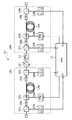
図1は本発明による光増幅器の構成例を示すブロック図である。光増幅器100は、1段目の光増幅部100aと、光可変減衰器110と、利得等化フィルタ111と、2段目の光増幅部100bとが順次に接続されている。また、この光増幅器100は、1段目および2段目の光増幅部における励起半導体レーザの駆動電流と光可変減衰器110の減衰量とを制御する制御器112をさらに備える。
FIG. 1 is a block diagram showing a configuration example of an optical amplifier according to the present invention. In the
1段目の光増幅部100aにおいて、入力された信号光を一方向に伝搬させる光アイソレータ102aと、信号光と励起光を合波する合波器103aと、増幅媒体とする、コアにエルビウムが添加されたエルビウム添加ファイバ104aと、増幅された信号光を一方向に伝搬させて出力する光アイソレータ105aとが順次に接続されている。また、エルビウム添加ファイバ104aへの励起光を発生させる励起光源とする半導体レーザ108aが、合波器103aに接続されている。加えて、光パワー検出値を制御器112に提供するために、1段目の光増幅部100aの入出力側にそれぞれ、光パワーの一部を分岐する分岐器101a、106aが挿入されており、さらに、光パワーを検出するフォトダイオード107a、109aが分岐器101a、106aに接続されている。2段目の光増幅部100bは、1段目の光増幅部100aと同様な構造としている。
In the first-stage optical amplifying
この構成例では、2つの光増幅部を有する光増幅器の構造を示したが、光増幅器は3つ以上の光増幅部を備えて、各光増幅部間に光可変減衰器および利得等化フィルタを備えることもできる。 In this configuration example, the structure of the optical amplifier having two optical amplifying units is shown. However, the optical amplifier includes three or more optical amplifying units, and an optical variable attenuator and a gain equalization filter are provided between the optical amplifying units. Can also be provided.
図1において、入力した信号光(複数波長が多重化されたWDM信号光)は、まず1段目の光増幅部100aで増幅された後、光可変減衰器110で減衰を受け、さらに利得等化フィルタ111を透過してその複数波長間の利得のばらつきが一定値以下に揃えられた後、2段目の光増幅部100bで増幅されて出力される。ここで、光可変減衰器110は、1波長あたりの入力信号光パワーに変化があった場合に、その変化量を補償するだけ減衰量を変化させることができる。それにより、後段の利得等化フィルタ111が入力信号光パワーの変化の影響を受けないように利得等化を行うことができる。従って、さらに後段の光増幅部100bで増幅されて出力される1波長あたりの出力信号光パワーは、1波長あたりの入力信号光パワーの変化に関わらず常に一定の値(制御誤差を含めると一定の範囲)となる。
In FIG. 1, input signal light (a WDM signal light in which a plurality of wavelengths are multiplexed) is first amplified by the first-stage
光増幅器100における制御器112は、各フォトダイオードで検出した光パワーに基づいて演算を実施し、その演算結果に基づいて励起光源である半導体レーザの駆動電流を調整するように機能する。以下に制御器112の動作を説明する。
The
入力された各光増幅部の入出力パワー検出値は制御器112において対数変換される。すなわち、それぞれ1段目の増幅入力側はP1、1段目の増幅出力側はP4、2段目の増幅入力側はP3、2段目の増幅出力側はP2と変換される。或いは、各フォトダイオードにおける検出値(電流値)を光電変換後、LOGアンプで増幅することにより、同様の対数値を得ることもできる。
The input / output power detection value of each optical amplification unit is logarithmically converted by the
制御器112は、1段目光増幅部の利得(P4−P1)と2段目光増幅部の利得(P2−P3)との合計値に対して、ASE補正値を加減算した結果が一定となるように、すなわち、
The
![]()
![]()
が成り立つように、1段目の光増幅部100aにおける半導体レーザ108aの駆動電流I1、及び2段目の光増幅部100bにおける半導体レーザ108bの駆動電流I2を制御する。ここで、Gagcは予め決めた固定の目標値である。前述のように、光可変減衰器は入力信号光パワーの変化量を補償するように減衰量が制御されるので、各光増幅部の励起半導体レーザを制御する際には入力信号光パワーの変化量を考慮する必要がなくなる。また、
So that the drive current I 1 of the
![]()
![]()
は、ASE補正値である。ここで、 Is an ASE correction value. here,
![]()
![]()
は、複数の光増幅器を用いた多中継光伝送システムに光増幅器を使用する場合に、自身より上流側の光増幅器で発生するASEに対する固定の補正値である。なお、 Is a fixed correction value for ASE generated in the optical amplifier upstream of itself when an optical amplifier is used in a multi-relay optical transmission system using a plurality of optical amplifiers. In addition,
![]()
![]()
は、光増幅器で発生するASEに対する補正値であり、その値が入力信号光のパワーP1に従って変化するので、P1の関数として表示される。 Is a correction value for ASE generated in the optical amplifier, and the value changes according to the power P 1 of the input signal light, and is thus displayed as a function of P 1 .
式(4)の値は、入力信号光パワーP1に従って変化するので、事前に一定の入力信号光パワーの間隔で計測して、制御器112内の記憶回路にテーブルとして保存しておく。それにより、制御器が入力信号光パワーの検出結果に従って保存したテーブルから式(4)の値を取得することができる。
Since the value of Expression (4) changes according to the input signal light power P 1, it is measured in advance at a constant input signal light power interval and stored as a table in the storage circuit in the
式(4)の誤差が大きくなると光増幅器制御誤差が大きくなるので、テーブル化に用いられる入力信号光パワーの間隔が入力信号光パワー検出精度(通常0.1dB程度)以下で式(4)の誤差が無いことが求められる。しかしながら、式(4)の誤差をなくすためには入力信号光パワー0.1dB毎に式(4)の値を制御器内の記憶回路にテーブル化すると、記憶回路の規模が大きくなる問題がある。従って、テーブル化に用いられる入力信号光パワーの間隔を広くする必要がある。 Since the optical amplifier control error increases as the error in Expression (4) increases, the interval of the input signal light power used for table formation is less than the input signal light power detection accuracy (usually about 0.1 dB), and Expression (4) It is required that there is no error. However, in order to eliminate the error of the equation (4), if the value of the equation (4) is tabulated in the memory circuit in the controller for every 0.1 dB of the input signal light power, there is a problem that the scale of the memory circuit becomes large. . Therefore, it is necessary to widen the interval between the input signal light powers used for table formation.
図2に入力信号光パワーの間隔に対する式(4)の誤差の依存性を示す。利得制御の検出精度も入力信号光パワー検出精度程度(通常0.1dB程度)であるので、式(4)の誤差は0.1dB以下に抑制する必要がある。図2から、入力信号光パワー間隔が3.8dB以下であれば、式(4)の誤差は0.1dB以下に抑制することができる。通常、入力信号光パワー間隔は整数であると演算などに都合が良い場合が多いため、入力信号光パワー間隔3dB以下で式(4)の値を記憶回路にテーブル化し、補間演算により所望の入力信号光パワーに対する式(4)の値を得ることが好ましい。一方で、制御器内の記憶回路規模が十分大きくて入力信号光パワー0.1dB毎にテーブル化できる場合も、式(4)の値を計測する際に入力信号光パワー間隔3dB以下で行うことにより、計測を簡略化することができる。 FIG. 2 shows the dependency of the error of equation (4) on the interval of the input signal light power. Since the detection accuracy of gain control is also about the input signal light power detection accuracy (usually about 0.1 dB), the error in equation (4) needs to be suppressed to 0.1 dB or less. From FIG. 2, if the input signal light power interval is 3.8 dB or less, the error of the equation (4) can be suppressed to 0.1 dB or less. Usually, an input signal light power interval is an integer, which is often convenient for calculations. Therefore, the value of equation (4) is tabulated in a memory circuit with an input signal light power interval of 3 dB or less, and desired input is performed by interpolation calculation. It is preferable to obtain the value of equation (4) for the signal light power. On the other hand, even when the storage circuit scale in the controller is sufficiently large and can be tabulated every 0.1 dB of the input signal light power, when the value of Equation (4) is measured, the input signal light power interval should be 3 dB or less. Thus, measurement can be simplified.
なお、光可変減衰器110の減衰量は、光増幅器全体の利得(P2−P1)に対して、ASE補正値を加減算した結果が、1波長あたりの入力信号光パワーに従って変化する利得目標値となるように、すなわち、 The attenuation amount of the optical variable attenuator 110 is a gain target in which the result of adding or subtracting the ASE correction value to the gain (P 2 -P 1 ) of the entire optical amplifier changes according to the input signal light power per wavelength. To be value, ie
![]()
![]()
を満たすように制御器112によって制御することができる。ここで、式(5)の左辺は、光可変減衰器の減衰量を含む、自身及び上流側で発生するASEを補正した光増幅器全体の利得である。また、右辺の
It can be controlled by the
![]()
![]()
は、1波長あたりの入力信号光パワーに従って変化する利得目標値であり、 Is a gain target value that varies according to the input signal light power per wavelength,
![]()
![]()
は、1波長あたりの入力信号光パワーである。光増幅器全体の利得目標値が1波長あたりの入力信号光パワーに従って変化するのは、1波長あたりの出力信号光パワーを一定に保つために1波長あたりの入力信号光パワーの変化量を補償するためである。その補償は、光可変減衰器の減衰量を制御することにより行う。 Is the input signal light power per wavelength. The gain target value of the entire optical amplifier changes according to the input signal light power per wavelength. In order to keep the output signal light power per wavelength constant, the amount of change in the input signal light power per wavelength is compensated. Because. The compensation is performed by controlling the attenuation amount of the optical variable attenuator.
さらに、式(1)とともに、式(5)について説明する。式(5)−式(1)から、 Furthermore, Formula (5) will be described together with Formula (1). From formula (5) -formula (1),
![]()
![]()
となる。式(8)の左辺の(P3−P4)は、利得等化フィルタ111から出力される信号光パワーの値と、光可変減衰器110に入力される信号光パワーの値との差である。すなわち、光可変減衰器110の減衰量と、利得等化フィルタ111による信号光パワーの増減値との和である。利得等化フィルタ111は所定の利得等化を行い、それによる信号光パワーの増減値が固定値であるので、(P3−P4)の変化は光可変減衰器110の減衰量の変化に相当する。式(8)の右辺第2項が固定値であるので、式(8)の右辺の変化は第1項の変化に相当し、すなわち、1波長あたりの入力信号光パワーに従って変化する。従って、式(8)は、1波長あたりの入力信号光パワーが大きく(小さく)なった場合、光可変減衰器の減衰量をその分だけ大きく(小さく)することを示している。すなわち、光可変減衰器は入力信号光パワーの変化量を補償するように減衰量が制御される。
It becomes. (P 3 −P 4 ) on the left side of Expression (8) is the difference between the value of the signal light power output from the
式(7)に示される1波長あたりの入力信号光パワーは、制御器がオペレーションシステムから波長数情報Nchを取得し、さらに The input signal light power per wavelength shown in Expression (7) is obtained by the controller acquiring the wavelength number information N ch from the operation system, and

から取得することができる。 Can be obtained from.
或いは、光増幅器の入力側の伝送ファイバ損失に変化があった場合に、信号光と波長の異なる監視信号光を用いることより、1波長あたりの入力信号光パワーの変化を制御器に提供することもできる。図3に監視波を用いた光増幅器の構成例を示す。光増幅器300は、図1の光増幅器100において、1段目の光増幅部の前段に監視信号光と信号光を分波する分波器313が挿入されおり、さらに、フォトダイオード314が分波器313に接続されている。図3において、監視信号光は、分波器313を介してフォトダイオード314に入力され、フォトダイオード314によって検出された監視波長の光パワー値が制御器に提供される。監視波長光パワーの変化は1波長あたりの入力信号光パワーの変化と等しくなるので、監視波長光パワー検出値P5を利用して、光増幅器全体の利得目標値はGalc(P5)とすることができる。図4は、光可変減衰器の減衰量制御時の利得目標値の変化の様子を示す概念図である。図4に示されるように、光増幅器全体の利得目標値は、1波長あたりの入力信号光パワーまたは監視波長光パワー(いずれもdBm単位換算)に対して、比例(負の比例係数)する値となる。
Alternatively, when there is a change in the transmission fiber loss on the input side of the optical amplifier, a change in input signal light power per wavelength is provided to the controller by using monitoring signal light having a wavelength different from that of the signal light. You can also. FIG. 3 shows a configuration example of an optical amplifier using a monitoring wave. In the
前述のように、1段目光増幅部の利得と2段目光増幅部の利得との合計値は式(1)を満たすように光増幅部の半導体レーザの駆動電流を制御する。それに加えて、1段目光増幅部と2段目光増幅部との間にもう1つの制約条件を設けて、光増幅部の半導体レーザの駆動電流をさらに制御し、その制約条件によって異なる制御方法となる。 As described above, the drive current of the semiconductor laser of the optical amplification unit is controlled so that the total value of the gain of the first-stage optical amplification unit and the gain of the second-stage optical amplification unit satisfies Equation (1). In addition, another constraint condition is provided between the first-stage optical amplification unit and the second-stage optical amplification unit to further control the driving current of the semiconductor laser of the optical amplification unit, and the control method varies depending on the constraint condition, Become.
図5は、駆動電流比一定制御における半導体レーザの駆動電流の制御方法を示す概念図である。I1は1段目光増幅部の半導体レーザの駆動電流であり、I2は2段目光増幅部の半導体レーザの駆動電流である。図5に示されるように、それぞれの半導体レーザの駆動電流リミット以下では、I1/I2が一定となるように制御される。それで、このような制御方法を駆動電流比一定制御と呼ぶ。一方で、1段目の光増幅部の半導体レーザの駆動電流I1、及び2段目の光増幅部の半導体レーザの駆動電流I2の制御方法としては、それぞれの光増幅部で利得一定となるように、すなわち、各光増幅部は利得平坦な増幅状態になるようにI1及びI2を制御する(以下、光増幅部平坦利得制御と呼ぶ)方法もある。以下に説明するように、駆動電流比一定制御の方が利点がある。 FIG. 5 is a conceptual diagram showing a method for controlling the drive current of the semiconductor laser in the constant drive current ratio control. I 1 is the drive current of the semiconductor laser of the first stage optical amplifier, and I 2 is the drive current of the semiconductor laser of the second stage optical amplifier. As shown in FIG. 5, control is performed so that I 1 / I 2 is constant below the drive current limit of each semiconductor laser. Therefore, such a control method is called constant drive current ratio control. On the other hand, as a method for controlling the driving current I 1 of the semiconductor laser of the first stage optical amplifying unit and the driving current I 2 of the semiconductor laser of the second stage optical amplifying unit, the gain is constant in each optical amplifying unit. In other words, there is a method of controlling I 1 and I 2 so that each optical amplifying unit is in a gain-flat amplification state (hereinafter referred to as optical amplifying unit flat gain control). As described below, the constant drive current ratio control has an advantage.
図6a、bに、駆動電流比一定制御と光増幅部平坦利得制御との各光増幅部利得の波長依存性を模式的に示している。ここで、駆動電流比一定制御と光増幅部平坦利得制御とで最大入力信号光パワーのときの駆動電流比R=I1/I2を同じとした。最大入力信号光パワーのとき、駆動電流比一定制御は光増幅部平坦利得制御と同じように、1段目の光増幅部及び2段目の光増幅部共に利得は波長に対して平坦な特性(平坦利得)となる(点線で示している利得曲線)。入力信号光パワーが最大値より小さくなると、光増幅部平坦利得制御では、1段目の光増幅部及び2段目の光増幅部共に利得は点線の利得曲線のまま変化しない。一方、駆動電流比一定制御では、実線の利得曲線で示されるように、1段目の光増幅部利得は増大(特に短波長側で大きく増大)し、2段目の光増幅部利得は減少(特に短波長側で大きく減少)する。しかしながら、結果として両者を合わせて平坦な利得特性が得られる。これは、駆動電流比一定のため、入力信号光パワーが低下したときに1段目の光増幅部では励起光パワーが過剰状態となる一方、2段目の光増幅部では励起光パワーが不足状態となるためである。 FIGS. 6A and 6B schematically show the wavelength dependence of each optical amplification unit gain in the constant drive current ratio control and the optical amplification unit flat gain control. Here, the drive current ratio R = I 1 / I 2 at the maximum input signal light power is the same for the constant drive current ratio control and the flat gain control of the optical amplifier. When the maximum input signal power is used, the constant drive current ratio control is the same as the optical amplifier flat gain control, and the gain is flat with respect to the wavelength in both the first optical amplifier and the second optical amplifier. (Flat gain) (gain curve shown by dotted line). When the input signal light power becomes smaller than the maximum value, in the optical amplification unit flat gain control, the gains of both the first-stage optical amplification unit and the second-stage optical amplification unit remain as the dotted gain curve. On the other hand, in the constant drive current ratio control, as shown by the solid line gain curve, the gain of the first-stage optical amplifier is increased (particularly increased on the short wavelength side) and the gain of the second-stage optical amplifier is decreased. (In particular, it is greatly reduced on the short wavelength side). However, as a result, a flat gain characteristic can be obtained by combining the two. This is because the drive current ratio is constant, and when the input signal light power decreases, the pump light power becomes excessive in the first stage optical amplifier, whereas the pump light power is insufficient in the second stage optical amplifier. It is because it will be in a state.
入力信号光パワーが最大値より小さいときの駆動電流比一定制御と光増幅部平坦利得制御との雑音指数を比較すると、図7に示されるように、駆動電流比一定制御の方が小さく、低雑音となる。1段目の光増幅部の利得、雑音指数をそれぞれG1、NF1、2段目の光増幅部の雑音指数をNF2、光可変減衰器の減衰量を含む1段目の光増幅部と2段目の光増幅部間の透過率をLとすると、光増幅器の雑音指数NFは Comparing the noise figure between the constant drive current ratio control and the optical gain flat gain control when the input signal light power is smaller than the maximum value, the constant drive current ratio control is smaller and lower as shown in FIG. It becomes noise. The gain and noise figure of the first stage optical amplifier are G 1 and NF 1 respectively, the noise figure of the second stage optical amplifier is NF 2 , and the first stage optical amplifier including the attenuation of the optical variable attenuator And the transmittance between the second stage optical amplifiers is L, the noise figure NF of the optical amplifier is
と表される。駆動電流比一定制御では、入力信号光パワーが小さくなると1段目の光増幅部利得G1が大きくなり、その結果、雑音指数NFが小さくなる。 It is expressed. In the constant drive current ratio control, when the input signal light power decreases, the first-stage optical amplifier gain G 1 increases, and as a result, the noise figure NF decreases.
一方で、入力信号光パワーが最大値より小さいときの駆動電流比一定制御と光増幅部平坦利得制御との励起光パワーを比較すると、図8に示されるように、駆動電流比一定制御の方が励起光パワーが大きくなる。しかしながら、光増幅器には最大入力信号光パワーのときに必要な励起光パワーを発生する半導体レーザを搭載しているので、それ以下の励起光パワーであれば問題なく発生させることができる。従って、駆動電流比一定制御では光増幅部平坦利得制御に比べて励起光パワーが大きくなることは問題とはならない。 On the other hand, when the excitation light power is compared between the constant drive current ratio control when the input signal light power is smaller than the maximum value and the optical gain flat gain control, the constant drive current ratio control is shown in FIG. However, the excitation light power is increased. However, since the optical amplifier is equipped with a semiconductor laser that generates the pumping light power required at the maximum input signal light power, any pumping light power lower than that can be generated without any problem. Therefore, in the constant drive current ratio control, it is not a problem that the pumping light power becomes larger than in the optical amplifier flat gain control.
ただし、入力信号光パワーが小さいときの励起光パワーを下げる必要がある場合は、励起光パワーが駆動電流比一定制御と光増幅部平坦利得制御とで同じになる入力信号光パワーを最大値から小さくすることにより、励起光パワーを下げることができる。図9において、その入力信号光パワーを However, if it is necessary to reduce the pumping light power when the input signal light power is low, the input signal light power that makes the pumping light power the same in the constant drive current ratio control and the optical gain flat gain control is maximized. By making it smaller, the pumping light power can be lowered. In FIG. 9, the input signal light power is
![]()
![]()
で示している。式(11)の入力信号光パワーは、駆動電流比一定制御の励起光パワー曲線と光増幅部平坦利得制御の励起光パワー曲線との交点の入力信号光パワーであるので、以下、交点入力信号光パワーと呼ぶ。また、図9の太線で示されるように、入力信号光パワーが交点入力信号光パワー以下では駆動電流比一定制御、交点入力信号光パワーより大きいときは光増幅部平坦利得制御に切り替えるようにする。それにより、低雑音性を得ることができる。この切替方式の雑音指数を図10において太線で示している。交点入力信号光パワーが最大値より小さい図9を、駆動電流比一定制御と光増幅部平坦利得制御とで最大入力信号光パワーのときの駆動電流比を同じとした、すなわち交点入力信号光パワーが最大値である図8と比較すると、交点入力信号光パワーを最大値から小さくすることにより、駆動電流比一定制御の励起光パワーを下げることができることがわかる。図10に示されるように、入力信号光パワーが交点入力信号光パワー以下では、駆動電流比一定制御の方が雑音指数が小さく、入力信号光パワーが交点入力信号光パワーより大きいとき、光増幅部平坦利得制御の方が雑音指数が小さい。従って、上記の切替方式により、低雑音性を得ることができる。なお、交点入力信号光パワーの値は、所望の励起光パワー特性と所望の雑音指数特性とに基づいて事前に決定することができる。 Is shown. Since the input signal light power in Expression (11) is the input signal light power at the intersection of the pumping light power curve with constant drive current ratio control and the pumping light power curve with optical amplifier flat gain control, the intersection input signal will be described below. Called optical power. Further, as shown by the thick line in FIG. 9, when the input signal light power is less than or equal to the intersection input signal light power, the drive current ratio constant control is performed, and when the input signal light power is greater than the intersection input signal light power, switching to the optical amplifier flat gain control is performed. . Thereby, low noise property can be obtained. The noise figure of this switching method is indicated by a thick line in FIG. In FIG. 9 in which the intersection input signal light power is smaller than the maximum value, the drive current ratio at the maximum input signal light power is the same in the constant drive current ratio control and the optical amplifier flat gain control. 8 is the maximum value, it can be seen that the excitation light power of the constant drive current ratio control can be reduced by reducing the intersection input signal light power from the maximum value. As shown in FIG. 10, when the input signal light power is equal to or less than the intersection input signal light power, the constant drive current ratio control has a smaller noise figure, and the input signal light power is larger than the intersection input signal light power. The noise figure is smaller in the partial flat gain control. Therefore, low noise can be obtained by the above switching method. Note that the value of the intersection input signal light power can be determined in advance based on the desired pumping light power characteristic and the desired noise figure characteristic.
前述のように、制御器は、式(1)及び式(2)の演算によってフィードバック制御を行う。それに加えて、信号波長数が急激に変化したときに入力信号光パワーが急変する場合、例えば、入力信号光パワー変化速度が±10dB/μs以上となる場合に、制御器は、フィードフォワードの駆動電流値IFをフィードバック制御の駆動電流に付加することができる。フィードフォワードの駆動電流値IFは、 As described above, the controller performs feedback control by the calculation of Expression (1) and Expression (2). In addition, when the input signal light power changes suddenly when the number of signal wavelengths changes suddenly, for example, when the input signal light power change speed is ± 10 dB / μs or more, the controller drives the feed forward. it can be added to the current value I F to the drive current of the feedback control. Feed forward drive current value IF is
![]()
![]()
と表され、ここで、 Where,
![]()
![]()
は、予め決めた固定値のフィードフォワード駆動電流値であり、 Is a feedforward drive current value of a fixed value determined in advance,
![]()
![]()
は、光パワー検出手段によって検出される入力信号光パワーに応じて変化するフィードフォワード駆動電流値であり、図11に示されるように入力信号光パワーに比例する。 Is a feedforward drive current value that changes according to the input signal light power detected by the optical power detection means, and is proportional to the input signal light power as shown in FIG.
このフィードフォワード制御をフィードバック制御に付加することにより、信号波長数が最大96波から1波に急激に減少したときに、出力信号光パワー(入力が変化しなかった1波の出力信号光パワー)の変動を0.2dBに抑圧することができる。それにより、フィードバック制御のみの1.5dBに比べ、出力信号光パワー変動を小さくする効果がみられた。 By adding this feedforward control to the feedback control, the output signal light power (the output signal light power of one wave whose input did not change) when the number of signal wavelengths rapidly decreases from a maximum of 96 waves to one wave. Can be suppressed to 0.2 dB. As a result, an effect of reducing the fluctuation of the output signal light power was seen as compared with 1.5 dB of only feedback control.
以上説明したように、本発明の光増幅器は、光伝送システムのスパンロスの変動や入力波長数の変化により入力信号光パワーの変化があっても、低雑音性を実現しながら利得の波長依存性を平坦に維持できると共に、利得の急激な変化を抑圧するという利点を有する。 As described above, the optical amplifier according to the present invention has a wavelength dependency of gain while realizing low noise even when there is a change in input signal light power due to a variation in span loss of the optical transmission system or a change in the number of input wavelengths. Can be maintained flat, and a sudden change in gain can be suppressed.
100、300 光増幅器
100a、300a 1段目光増幅部
100b、300b 2段目光増幅部
101a、106a、101b、106b、301a、306a、301b、306b 分岐器
102a、105a、102b、105b、302a、305a、302b、305b 光アイソレータ
103a、103b、303a、303b 合波器
104a、104b、304a、304b エルビウム添加ファイバ
107a、109a、107b、109b、307a、309a、307b、309b、314 フォトダイオード
108a、108b、308a、308b 半導体レーザ
110、310 光可変減衰器
111、311 利得等化フィルタ
112、312 制御器
313 分波器
100, 300
Claims (9)
前記光パワー検出手段の検出結果に基づいて、各光増幅部の出力信号光パワー検出値と入力信号光パワー検出値との差である各光増幅部の利得の合計値に対して、増幅自然放出光(ASE:Amplified Spontaneous Emission)補正値を加減算した結果が予め決めた固定の目標値となるように、前記各光増幅部の半導体レーザへの駆動電流を制御するように構成された制御手段をさらに備え、
前記制御手段は、第1段の光増幅部の入力信号光パワー検出値が所定の入力信号光パワー値以下の場合に、各光増幅部の半導体レーザへの駆動電流の比が一定である制御と、前記第1段の光増幅部の入力信号光パワー検出値が前記所定の入力信号光パワー値より大きい場合に、前記各光増幅部の利得の波長依存性を平坦にする制御とを切り替えるように構成され、
前記所定の入力信号光パワー値は、前記各光増幅部の入力信号光パワーが最大値より小さい場合に、前記駆動電流の比が一定である制御と前記利得の波長依存性を平坦にする制御とで励起光パワーが同一となる入力信号光パワー値であり、
各光増幅部は、入力信号光パワーが前記最大値より小さく且つ前記所定の入力信号光パワー値より小さい場合、前記駆動電流の比が一定である制御における励起光パワーが前記利得の波長依存性を平坦にする制御における励起光パワーより大きくなる特性を有し、
各光増幅部への入力信号光パワーが前記最大値より小さく且つ前記駆動電流比が一定である場合、前記第1段の光増幅部の励起光パワーが過剰状態となり、第2段の光増幅部の励起光パワーが不足状態となることを特徴とする光増幅器。 An erbium-doped fiber that amplifies signal light, a semiconductor laser that generates pump light to the erbium-doped fiber, a multiplexer that combines the signal light and the pump light, and input signal light of the erbium-doped fiber Two or more optical amplifying units including optical power detection means for detecting power and output signal optical power,
Based on the detection result of the optical power detector, the natural amplification is performed with respect to the total gain of each optical amplifying unit, which is the difference between the output signal optical power detection value of each optical amplifying unit and the input signal optical power detection value. Control means configured to control the drive current to the semiconductor laser of each of the optical amplifying units so that the result of adding and subtracting the emission light (ASE: Amplified Spontaneous Emission) correction value becomes a predetermined fixed target value. Further comprising
The control means controls the ratio of the drive current to the semiconductor laser of each optical amplifying unit to be constant when the input signal optical power detection value of the first stage optical amplifying unit is less than or equal to a predetermined input signal optical power value. If, when the input signal light power detection value of the optical amplification portion of the first stage is larger Ri by said predetermined input signal light power value, and a control to flatten the wavelength dependence of the gain of each optical amplifier Configured to switch ,
The predetermined input signal light power value is a control in which the ratio of the drive current is constant and a control for flattening the wavelength dependence of the gain when the input signal light power of each of the optical amplifiers is smaller than the maximum value. And the input signal light power value at which the pumping light power is the same,
Each optical amplifying unit is configured such that when the input signal light power is smaller than the maximum value and smaller than the predetermined input signal light power value, the pump light power in the control in which the ratio of the drive current is constant depends on the wavelength dependence of the gain. Has a characteristic that becomes larger than the pumping light power in the control of flattening,
When the input signal light power to each optical amplifying unit is smaller than the maximum value and the drive current ratio is constant, the pumping light power of the first stage optical amplifying part becomes an excessive state, and the second stage optical amplification An optical amplifier characterized in that the pumping light power of the part is in an insufficient state .
前記2つ以上の光増幅部の間に、前記光増幅器に入力される信号光のパワーの変化を補償するように減衰量が調整されて信号光の減衰を行う光可変減衰器と、前記光可変減衰器で減衰を受けた信号光に対して利得等化を行う利得等化フィルタとをさらに備え、
前記制御手段は、前記光可変減衰器の減衰量を調整するようにさらに構成され、前記減衰量は、前記光パワー検出手段の検出結果に基づいて、最終段の光増幅部の出力信号光パワー検出値と前記第1段の光増幅部の入力信号光パワー検出値との差である、前記減衰量を含む前記光増幅器全体の利得に対して、前記ASE補正値を加減算した結果が、1波長あたりの入力信号光パワーに従って変化する利得目標値となるように調整され、前記利得目標値は前記1波長あたりの入力信号光パワーの演算によって取得されることを特徴とする請求項1に記載の光増幅器。 In at least one of the two or more optical amplification units, the optical amplification unit further includes an optical isolator in a front stage of the multiplexer and / or a rear stage of the erbium-doped fiber,
An optical variable attenuator that attenuates signal light by adjusting an attenuation amount so as to compensate for a change in power of the signal light input to the optical amplifier between the two or more optical amplification units, and the light A gain equalization filter that performs gain equalization on the signal light attenuated by the variable attenuator;
The control means is further configured to adjust the attenuation amount of the optical variable attenuator, and the attenuation amount is determined based on the detection result of the optical power detection means, and the output signal optical power of the final stage optical amplifying unit. The result of adding / subtracting the ASE correction value to / from the gain of the entire optical amplifier including the attenuation amount, which is the difference between the detection value and the input signal optical power detection value of the first stage optical amplification unit, is 1 2. The gain target value is adjusted so as to change according to input signal light power per wavelength, and the gain target value is obtained by calculating the input signal light power per wavelength. Optical amplifier.
前記1波長あたりの入力信号光パワーは、前記監視波長光パワー検出手段によって検出された監視波長の光パワーから取得されることを特徴とする請求項2に記載の光増幅器。 A demultiplexer for demultiplexing the monitoring wavelength light and the signal light is inserted before the first stage optical amplifying unit, and a photodiode is connected to the demultiplexer. Further comprising a monitoring wavelength optical power detection means for detecting the optical power of
3. The optical amplifier according to claim 2, wherein the input signal light power per wavelength is obtained from the optical power of the monitoring wavelength detected by the monitoring wavelength optical power detection unit.
Priority Applications (1)
| Application Number | Priority Date | Filing Date | Title |
|---|---|---|---|
| JP2011003305A JP5584143B2 (en) | 2011-01-11 | 2011-01-11 | Optical amplifier |
Applications Claiming Priority (1)
| Application Number | Priority Date | Filing Date | Title |
|---|---|---|---|
| JP2011003305A JP5584143B2 (en) | 2011-01-11 | 2011-01-11 | Optical amplifier |
Publications (2)
| Publication Number | Publication Date |
|---|---|
| JP2012146785A JP2012146785A (en) | 2012-08-02 |
| JP5584143B2 true JP5584143B2 (en) | 2014-09-03 |
Family
ID=46790077
Family Applications (1)
| Application Number | Title | Priority Date | Filing Date |
|---|---|---|---|
| JP2011003305A Expired - Fee Related JP5584143B2 (en) | 2011-01-11 | 2011-01-11 | Optical amplifier |
Country Status (1)
| Country | Link |
|---|---|
| JP (1) | JP5584143B2 (en) |
Families Citing this family (5)
| Publication number | Priority date | Publication date | Assignee | Title |
|---|---|---|---|---|
| WO2014068776A1 (en) * | 2012-11-02 | 2014-05-08 | 富士通株式会社 | Raman amplifier and gain control method |
| JP6519117B2 (en) * | 2014-08-04 | 2019-05-29 | 富士通株式会社 | Optical transmission apparatus, optical transmission system, and control apparatus for optical transmission system |
| WO2019169642A1 (en) | 2018-03-09 | 2019-09-12 | 华为技术有限公司 | Optical fiber amplifier and optical fiber amplifier gain adjustment method |
| CN112366501A (en) * | 2020-10-21 | 2021-02-12 | 昂纳信息技术(深圳)有限公司 | Erbium-doped optical fiber amplifier with wide gain adjustable range |
| CN114499673A (en) * | 2020-11-12 | 2022-05-13 | 莫列斯有限公司 | Optical amplifier module and gain control method thereof |
Family Cites Families (9)
| Publication number | Priority date | Publication date | Assignee | Title |
|---|---|---|---|---|
| KR100276756B1 (en) * | 1996-12-31 | 2001-01-15 | 강병호 | Gain Flattened Fiber Optic Amplifier |
| US6215584B1 (en) * | 1999-05-10 | 2001-04-10 | Jds Uniphase Inc. | Input independent tilt free actively gain flattened broadband amplifier |
| JP2000349718A (en) * | 1999-06-08 | 2000-12-15 | Nec Corp | Optical fiber amplifier |
| JP2001284689A (en) * | 2000-04-04 | 2001-10-12 | Nippon Telegr & Teleph Corp <Ntt> | Optical amplifier |
| JP4595210B2 (en) * | 2001-02-14 | 2010-12-08 | 株式会社日立製作所 | Configuration and control method of optical amplifier or add / drop multiplexer in wavelength division multiplexing optical network |
| JP4026458B2 (en) * | 2002-09-19 | 2007-12-26 | 日本電気株式会社 | Gain equalizer and WDM optical repeater system |
| JP3977287B2 (en) * | 2003-06-12 | 2007-09-19 | 古河電気工業株式会社 | Optical fiber amplifier |
| JP4663997B2 (en) * | 2004-03-09 | 2011-04-06 | 富士通株式会社 | Optical transmission equipment using wide input dynamic range optical amplifier |
| GB0413017D0 (en) * | 2004-06-10 | 2004-07-14 | Bookham Technology Plc | Optical amplifiers |
-
2011
- 2011-01-11 JP JP2011003305A patent/JP5584143B2/en not_active Expired - Fee Related
Also Published As
| Publication number | Publication date |
|---|---|
| JP2012146785A (en) | 2012-08-02 |
Similar Documents
| Publication | Publication Date | Title |
|---|---|---|
| JP4388705B2 (en) | Optical amplifier | |
| JP5239141B2 (en) | Optical amplification device and control method thereof | |
| JP3903650B2 (en) | Optical amplifier and optical amplifier control method | |
| US7085043B2 (en) | Optical amplifier | |
| US7715092B2 (en) | Dynamic raman tilt compensation | |
| JP2000252923A (en) | Optical amplifier for wavelength multiplexing and optical communication system | |
| JP2016208310A (en) | Optical transmission system and optical transmission device | |
| JP5584143B2 (en) | Optical amplifier | |
| JPH11275021A (en) | Optical amplifier | |
| JP3817565B2 (en) | Optical amplifier | |
| US8351112B2 (en) | Optical amplifier | |
| EP3654552B1 (en) | Tilt control through optical pump power adjustment | |
| US8428463B2 (en) | Apparatus and method for controlling a dynamic gain equalizer | |
| JP4666364B2 (en) | Optical amplifier | |
| JP3551418B2 (en) | Optical transmission device and wavelength division multiplexing optical communication system | |
| JP5239223B2 (en) | Optical amplifier | |
| JP4192364B2 (en) | Optical amplifier | |
| JP4484565B2 (en) | Multistage optical amplifier with tilt compensation function | |
| JP5304378B2 (en) | Optical amplifier | |
| JP2003258346A (en) | Light amplifier and attenuation adjusting method | |
| JP2009164565A (en) | Gain equalizer, optical amplifier, and optical amplification method | |
| JP3551417B2 (en) | Optical amplifier for wavelength multiplexing | |
| JP2000114629A (en) | Optical amplifier | |
| JP4580404B2 (en) | Optical amplifier | |
| JP2012043934A (en) | Amplification device, communication system and amplification method |
Legal Events
| Date | Code | Title | Description |
|---|---|---|---|
| A621 | Written request for application examination |
Free format text: JAPANESE INTERMEDIATE CODE: A621 Effective date: 20121212 |
|
| A977 | Report on retrieval |
Free format text: JAPANESE INTERMEDIATE CODE: A971007 Effective date: 20131127 |
|
| A131 | Notification of reasons for refusal |
Free format text: JAPANESE INTERMEDIATE CODE: A131 Effective date: 20131217 |
|
| A521 | Written amendment |
Free format text: JAPANESE INTERMEDIATE CODE: A523 Effective date: 20140213 |
|
| A131 | Notification of reasons for refusal |
Free format text: JAPANESE INTERMEDIATE CODE: A131 Effective date: 20140304 |
|
| RD13 | Notification of appointment of power of sub attorney |
Free format text: JAPANESE INTERMEDIATE CODE: A7433 Effective date: 20140404 |
|
| A521 | Written amendment |
Free format text: JAPANESE INTERMEDIATE CODE: A821 Effective date: 20140404 |
|
| A521 | Written amendment |
Free format text: JAPANESE INTERMEDIATE CODE: A523 Effective date: 20140424 |
|
| TRDD | Decision of grant or rejection written | ||
| A01 | Written decision to grant a patent or to grant a registration (utility model) |
Free format text: JAPANESE INTERMEDIATE CODE: A01 Effective date: 20140715 |
|
| A61 | First payment of annual fees (during grant procedure) |
Free format text: JAPANESE INTERMEDIATE CODE: A61 Effective date: 20140717 |
|
| R150 | Certificate of patent or registration of utility model |
Ref document number: 5584143 Country of ref document: JP Free format text: JAPANESE INTERMEDIATE CODE: R150 |
|
| LAPS | Cancellation because of no payment of annual fees |