JP5579477B2 - Overcurrent prevention type power supply device and lighting fixture using the same - Google Patents

Overcurrent prevention type power supply device and lighting fixture using the same Download PDF

Info

Publication number
JP5579477B2
JP5579477B2 JP2010073509A JP2010073509A JP5579477B2 JP 5579477 B2 JP5579477 B2 JP 5579477B2 JP 2010073509 A JP2010073509 A JP 2010073509A JP 2010073509 A JP2010073509 A JP 2010073509A JP 5579477 B2 JP5579477 B2 JP 5579477B2
Authority
JP
Japan
Prior art keywords
unit
voltage
current
constant
output
Prior art date
Legal status (The legal status is an assumption and is not a legal conclusion. Google has not performed a legal analysis and makes no representation as to the accuracy of the status listed.)
Expired - Fee Related
Application number
JP2010073509A
Other languages
Japanese (ja)
Other versions
JP2011205868A (en
Inventor
正徳 三嶋
大志 城戸
正平 山本
将直 大川
洋史 小西
勝信 濱本
Current Assignee (The listed assignees may be inaccurate. Google has not performed a legal analysis and makes no representation or warranty as to the accuracy of the list.)
Panasonic Corp
Panasonic Holdings Corp
Original Assignee
Panasonic Corp
Matsushita Electric Industrial Co Ltd
Priority date (The priority date is an assumption and is not a legal conclusion. Google has not performed a legal analysis and makes no representation as to the accuracy of the date listed.)
Filing date
Publication date
Application filed by Panasonic Corp, Matsushita Electric Industrial Co Ltd filed Critical Panasonic Corp
Priority to JP2010073509A priority Critical patent/JP5579477B2/en
Publication of JP2011205868A publication Critical patent/JP2011205868A/en
Application granted granted Critical
Publication of JP5579477B2 publication Critical patent/JP5579477B2/en
Expired - Fee Related legal-status Critical Current
Anticipated expiration legal-status Critical

Links

Images

Classifications

    • YGENERAL TAGGING OF NEW TECHNOLOGICAL DEVELOPMENTS; GENERAL TAGGING OF CROSS-SECTIONAL TECHNOLOGIES SPANNING OVER SEVERAL SECTIONS OF THE IPC; TECHNICAL SUBJECTS COVERED BY FORMER USPC CROSS-REFERENCE ART COLLECTIONS [XRACs] AND DIGESTS
    • Y02TECHNOLOGIES OR APPLICATIONS FOR MITIGATION OR ADAPTATION AGAINST CLIMATE CHANGE
    • Y02BCLIMATE CHANGE MITIGATION TECHNOLOGIES RELATED TO BUILDINGS, e.g. HOUSING, HOUSE APPLIANCES OR RELATED END-USER APPLICATIONS
    • Y02B20/00Energy efficient lighting technologies, e.g. halogen lamps or gas discharge lamps
    • Y02B20/40Control techniques providing energy savings, e.g. smart controller or presence detection

Description

本発明は、過電流防止式電源装置とそれを用いた照明器具に関する。   The present invention relates to an overcurrent prevention type power supply device and a lighting fixture using the same.

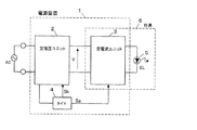
従来の、この種の電源装置を用いた照明器具の例を図12(例えば、特許文献1参照)に示す。この照明器具は、光源部である照明負荷11と点灯装置12からなり、点灯装置12は、整流回路部13と、PFC(力率改善)回路部(定電圧ユニットに相当)14と、電流出力部(定電流ユニットに相当)15と、調光回路部16とを備える。   An example of a conventional lighting fixture using this type of power supply device is shown in FIG. 12 (see, for example, Patent Document 1). This lighting fixture includes a lighting load 11 as a light source unit and a lighting device 12. The lighting device 12 includes a rectifier circuit unit 13, a PFC (power factor correction) circuit unit (corresponding to a constant voltage unit) 14, and a current output. Unit (corresponding to a constant current unit) 15 and a light control circuit unit 16.

PFC回路部14は、チョークコイルL1、FETからなるスイッチング素子Q1、ソース抵抗R1、ダイオードD1、及びコンデンサC1から成る昇圧チョッパ回路と、PFC制御部17とからなり、定電圧を電流出力部15に出力する定電圧源となっている。   The PFC circuit unit 14 includes a choke coil L1, a switching element Q1 composed of an FET, a source resistor R1, a diode D1, and a capacitor C1, and a PFC control unit 17, and a constant voltage is supplied to the current output unit 15. It is a constant voltage source for output.

電流出力部15は、スイッチング素子Q2、チョークコイルL3、ダイオードD2、及びコンデンサC2から成る降圧チョッパ回路と、電流検出用の抵抗R6と、電流制御部18とからなり、照明負荷11に定電流を出力する定電流源となっている。調光回路部16は調光制御部19によってスイッチング素子Q3を駆動し照明負荷11を調光する。 The current output unit 15 includes a step-down chopper circuit including a switching element Q2 , a choke coil L3, a diode D2, and a capacitor C2, a current detection resistor R6, and a current control unit 18, and supplies a constant current to the illumination load 11. It is a constant current source that outputs. The dimming circuit unit 16 controls the lighting load 11 by driving the switching element Q3 by the dimming control unit 19.

上記照明器具においては、交流電源(AC)から給電されたPFC回路部14からの出力電圧を基に電流出力部15が定電流動作して一定電流を照明負荷に供給する。このとき、PFC回路部14と電流出力部15との動作状態が合わないと、起動時に流れる過電流によって、起動不良を起したり、ときにはPFC回路部14等の各回路素子にそれらの定格以上の電流、電圧のストレスが掛かり、回路素子が損傷する場合がある。   In the lighting apparatus, the current output unit 15 operates at a constant current based on the output voltage from the PFC circuit unit 14 fed from an AC power supply (AC) and supplies a constant current to the lighting load. At this time, if the operating states of the PFC circuit unit 14 and the current output unit 15 do not match, an overcurrent flowing at the time of start-up causes a start-up failure, or sometimes each circuit element such as the PFC circuit unit 14 exceeds the rating. Current and voltage stress may be applied, and circuit elements may be damaged.

以下にその動作を説明する。交流電源の投入直後は、PFC回路部14のコンデンサC1が充電されていないし、電流出力部15のコイルL3にも電流が流れていない。従って、交流電源(AC)の投入直後は、図13(a)に示すように、コンデンサC1の電圧Vは、時間t1で整流回路部13からの電圧V1により充電された後に、PCF制御部17が動作開始する時間t3から上昇が始まり、時間経過と共に、PFC制御部17で定める所望の電圧Voまで昇圧しようとする。電圧V1は、交流電源のピーク値電圧であり、AC100ボルト(V)の場合は、約141V程度である。   The operation will be described below. Immediately after the AC power is turned on, the capacitor C1 of the PFC circuit unit 14 is not charged, and no current flows through the coil L3 of the current output unit 15. Therefore, immediately after the AC power supply (AC) is turned on, the voltage V of the capacitor C1 is charged with the voltage V1 from the rectifier circuit unit 13 at time t1, as shown in FIG. Starts to rise from time t3 when the operation starts, and as time elapses, it tries to boost the voltage to a desired voltage Vo determined by the PFC control unit 17. The voltage V1 is a peak value voltage of the AC power supply, and is about 141 V in the case of AC 100 volts (V).

電流制御部18は、抵抗R6による電流検出電圧を基に、電流出力部15の出力が所望の定格電流になるように制御する。このため、電流制御部18がコンデンサC1の電圧が低い領域において定電流制御を開始すると、ピーク値の大きい過電流を電源となるコンデンサC1から引き出すことになる。   The current control unit 18 controls the output of the current output unit 15 to be a desired rated current based on the current detection voltage by the resistor R6. For this reason, when the current control unit 18 starts constant current control in a region where the voltage of the capacitor C1 is low, an overcurrent having a large peak value is drawn from the capacitor C1 serving as a power source.

例えば、図13(b)に示すように、PFC回路部14が動作を開始しているときの時間tpで、電流出力部15が定電流動作が開始すると、そのピーク電流Ipeakによって、コンデンサC1から過電流が引き出され、PFC制御部17のフィードバック検出量が急激に大きくなって、制御の許容範囲を超えるようになる。このため、PFC制御部17の動作自体が機能せず異常状態となり、IC回路による異常検出機能等によってPFC回路部14のチョッパ回路動作が停止してしまう場合が生じる。また、このチョッパ回路動作の停止により、時間tp以降は再び電圧V1に戻って昇圧できなくなる。   For example, as shown in FIG. 13B, when the current output unit 15 starts constant current operation at time tp when the PFC circuit unit 14 starts operation, the peak current Ipeak causes the capacitor C1 to Overcurrent is drawn, and the amount of feedback detected by the PFC control unit 17 suddenly increases and exceeds the allowable control range. For this reason, the operation of the PFC control unit 17 does not function and an abnormal state occurs, and the chopper circuit operation of the PFC circuit unit 14 may be stopped due to an abnormality detection function or the like by the IC circuit. Further, due to the stop of the chopper circuit operation, the voltage returns to the voltage V1 again after the time tp and cannot be boosted.

このとき、時間t4以降、電流出力部15への入力供給電圧が電圧V1に固定されてしまい、本来なら定格の電流値Io2に低減させたいにも拘らず、高い電流Io1を維持したままとなり、各素子へのストレスが大きくなる。そのため、IC回路等の異常検出機能により電流出力部15そのものを強制的に停止させることができるが、点線で示すように、出力電流Iがゼロに低下するので照明負荷11を点灯できなくなる。   At this time, the input supply voltage to the current output unit 15 is fixed at the voltage V1 after the time t4, and the high current Io1 is maintained even though it is originally intended to be reduced to the rated current value Io2. The stress on each element increases. For this reason, the current output unit 15 itself can be forcibly stopped by an abnormality detection function such as an IC circuit. However, as indicated by a dotted line, the output current I is reduced to zero, so that the illumination load 11 cannot be turned on.

特に、PFC制御の場合は、突入電流を防止するために、コンデンサC1への充電を徐々に行うソフトスタート機能などが採用される場合が多いため、電流出力部15が充電途中などに、より低電圧で起動し、過電流が発生し易くなる。   In particular, in the case of PFC control, in order to prevent an inrush current, a soft start function that gradually charges the capacitor C1 is often employed, so that the current output unit 15 is lower during charging. Starting with voltage, overcurrent is likely to occur.

また、点灯装置が交流電源、整流回路部13、及びPFC回路部14からなる定電圧ユニットと、電流出力部15及び調光回路部16からなる定電流ユニットとに分かれて接続されるような場合には、定電流ユニット内の各制御回路用電源は、定電圧ユニットの出力電圧を利用して形成される。このとき、起動のシーケンスがPFC制御部17、電流制御部18の順となり、上記のピーク電流による定電圧動作停止等の問題が顕著になる。   Further, when the lighting device is divided and connected to a constant voltage unit composed of an AC power source, a rectifier circuit unit 13 and a PFC circuit unit 14 and a constant current unit composed of a current output unit 15 and a dimming circuit unit 16 The power source for each control circuit in the constant current unit is formed using the output voltage of the constant voltage unit. At this time, the startup sequence is in the order of the PFC control unit 17 and the current control unit 18, and problems such as the constant voltage operation stop due to the peak current become remarkable.

また、定電圧ユニットと定電流ユニットが別々の場合に、1つの定電圧ユニットに複数の定電流ユニットが接続される場合は、コンデンサC1から流れる過電流が更に増大することになる。   In addition, when the constant voltage unit and the constant current unit are separate, when a plurality of constant current units are connected to one constant voltage unit, the overcurrent flowing from the capacitor C1 further increases.

特開2009−80995号公報JP 2009-80995 A

本発明は、上記問題を解消するもので、定電圧ユニットからの電圧を受けて駆動される定電流ユニットにより照明負荷を点灯する過電流防止式電源装置において、定電圧ユニットによる電圧供給開始後の定電流ユニットの起動に伴う過電流により定電圧ユニットの制御動作が停止されることを防止する過電流防止式電源装置及び照明器具を提供することを目的とする。   The present invention solves the above-described problem. In an overcurrent prevention type power supply device that lights a lighting load by a constant current unit driven by receiving a voltage from a constant voltage unit, the voltage after the voltage supply start by the constant voltage unit is started. An object of the present invention is to provide an overcurrent prevention type power supply device and a lighting fixture that prevent a control operation of a constant voltage unit from being stopped due to an overcurrent associated with activation of the constant current unit.

上記目的を達成するために本発明の過電流防止式電源装置は、一定電圧を出力する定電圧ユニットと、前記定電圧ユニットからの電圧を受けて駆動される定電流ユニットと、前記定電圧ユニットへの電圧供給開始後の経過時間を計測するためのタイマと、を備え、前記定電流ユニットは、前記タイマにより計測される経過時間が予め定められた一定時間を経過する前に動作を開始することを特徴とする。 In order to achieve the above object, an overcurrent prevention type power supply apparatus according to the present invention includes a constant voltage unit that outputs a constant voltage, a constant current unit that is driven by receiving a voltage from the constant voltage unit, and the constant voltage unit. A timer for measuring an elapsed time after the start of voltage supply to the constant current unit, and the constant current unit starts an operation before an elapsed time measured by the timer passes a predetermined time It is characterized by that.

この過電流防止式電源装置において、タイマを複数有し、タイマは、定電流ユニットと定電圧ユニットとに、それぞれの動作開始のための信号を伝達することが好ましい。 This overcurrent prevention type power supply device preferably has a plurality of timers, and the timers preferably transmit signals for starting their operations to the constant current unit and the constant voltage unit.

この過電流防止式電源装置において、定電圧ユニットは、入力電圧を昇圧する昇圧チョッパ回路と、昇圧チョッパ回路を駆動するための制御回路とを有し、制御回路は、昇圧チョッパ回路の動作開始時間を、定電流ユニットの動作開始時間より遅くすることが好ましい。   In this overcurrent prevention type power supply device, the constant voltage unit has a boost chopper circuit that boosts the input voltage and a control circuit for driving the boost chopper circuit, and the control circuit has an operation start time of the boost chopper circuit. Is preferably later than the operation start time of the constant current unit.

本発明の照明器具は、上記のような過電流防止式電源装置と、照明負荷と、電源装置と照明負荷とを接続する接続部と、を備えたことを特徴とする。   The lighting fixture of the present invention includes the above-described overcurrent-preventing power supply device, a lighting load, and a connection portion that connects the power supply device and the lighting load.

本発明の過電流防止式電源装置によれば、タイマを用い、予め定められた一定時間を定電圧ユニットが動作開始するまでの時間として、定電流ユニットが一定時間前に動作開始するようにできる。従って、定電流ユニットの動作開始時のピーク電流による過電流の影響により定電圧ユニットの定電圧動作が停止されることを防止することができ、回路全体を起動することができる。   According to the overcurrent prevention type power supply device of the present invention, a constant current unit can be started to operate a certain time before using a timer as a time until the constant voltage unit starts to operate. . Therefore, it is possible to prevent the constant voltage operation of the constant voltage unit from being stopped due to the influence of the overcurrent due to the peak current at the start of the operation of the constant current unit, and to start up the entire circuit.

本発明の第1の実施形態に係る過電流防止式電源装置を用いた照明器具の構成図。The block diagram of the lighting fixture using the overcurrent prevention type power supply device which concerns on the 1st Embodiment of this invention. 同実施形態の装置における定電圧ユニットの回路図。The circuit diagram of the constant voltage unit in the apparatus of the embodiment. 同実施形態の装置における定電流ユニットの回路図。The circuit diagram of the constant current unit in the apparatus of the embodiment. (a)は同定電圧ユニットの出力電圧波形を示す図、(b)は同定電流ユニットの出力電流波形を示す図、(c)はタイマにおけるカウンタの出力電圧波形を示す図、(d)はタイマにおける他のカウンタの出力電圧波形を示す図。(A) is a figure which shows the output voltage waveform of an identification voltage unit, (b) is a figure which shows the output current waveform of an identification current unit, (c) is a figure which shows the output voltage waveform of the counter in a timer, (d) is a timer The figure which shows the output voltage waveform of the other counter in. 同実施形態の変形例における定電圧ユニットの構成図。The block diagram of the constant voltage unit in the modification of the embodiment. 同定電圧ユニットの回路図。The circuit diagram of an identification voltage unit. (a)は同定電圧ユニットの昇圧チョッパ部の出力波形を示す図、(b)は同定電圧ユニットの降圧チョッパ部の出力波形を示す図、(c)は同定電流ユニットの出力電流波形を示す図。(A) is a figure which shows the output waveform of the step-up chopper part of an identification voltage unit, (b) is a figure which shows the output waveform of the step-down chopper part of an identification voltage unit, (c) is a figure which shows the output current waveform of an identification current unit . 本発明の第2の実施形態に係る装置における定電圧ユニットの回路図。The circuit diagram of the constant voltage unit in the apparatus which concerns on the 2nd Embodiment of this invention. 同実施形態の装置における定電流ユニットの回路図。The circuit diagram of the constant current unit in the apparatus of the embodiment. 本発明の第3の実施形態に係る装置を用いた照明器具の構成図。The block diagram of the lighting fixture using the apparatus which concerns on the 3rd Embodiment of this invention. 同照明器具の他の形態を示す斜視図。The perspective view which shows the other form of the lighting fixture. 従来の照明器具の構成図。The block diagram of the conventional lighting fixture. (a)は同照明器具におけるPFC回路部の出力電圧波形を示す図、(b)は同照明器具における電流出力部の出力電流波形を示す図。(A) is a figure which shows the output voltage waveform of the PFC circuit part in the lighting fixture, (b) is a figure which shows the output current waveform of the current output part in the lighting fixture.

(第1の実施形態)
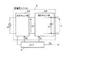
本発明の実施形態に係る過電流防止式電源装置について図1乃至図4を参照して説明する。図1に示すように、本実施形態の過電流防止式電源装置1(以下、電源装置という)は、交流電源(AC)から給電されて一定電圧を出力する定電圧ユニット2と、定電圧ユニット2からの電圧を受けて照明負荷5を点灯駆動する定電流ユニット3と、タイマ4とを備える。タイマ4は、定電圧ユニット2による電圧供給開始後の経過時間を計測する。ここでは、電源装置1と照明負荷5とは、照明器具を構成する。定電流ユニット3と照明負荷5とを一体としたものを灯具6とし、定電圧ユニット2と灯具6とを分離して配線する照明器具の形態も可能である。タイマ4は定電圧ユニット2または定電流ユニット3に内蔵することができる。
(First embodiment)
An overcurrent prevention type power supply device according to an embodiment of the present invention will be described with reference to FIGS. As shown in FIG. 1, an overcurrent prevention type power supply device 1 (hereinafter referred to as a power supply device) of this embodiment includes a constant voltage unit 2 that is supplied with power from an AC power supply (AC) and outputs a constant voltage, and a constant voltage unit. 2 is provided with a constant current unit 3 that receives the voltage from 2 and drives the lighting load 5 to light and a timer 4. The timer 4 measures the elapsed time after starting the voltage supply by the constant voltage unit 2. Here, the power supply device 1 and the lighting load 5 constitute a lighting fixture. A configuration in which the constant current unit 3 and the lighting load 5 are integrated into the lamp 6 and the constant voltage unit 2 and the lamp 6 are separated and wired is also possible. The timer 4 can be built in the constant voltage unit 2 or the constant current unit 3.

照明負荷5は、有機EL発光素子を用いているが、LED発光素子などの他の固体発光素子を含め、直流で点灯する光源であればよい。   The illumination load 5 uses an organic EL light emitting element, but may be any light source that is lit with a direct current, including other solid light emitting elements such as LED light emitting elements.

図2に示すように、定電圧ユニット2は、入力部(接続部)20と、ローパスフィルタ(LPF)21と、整流回路部22と、制御電源回路23と、昇圧チョッパ部(昇圧チョッパ回路)24と、出力部(接続部)25とを有する。入力部20は交流電源(AC)に接続され、LPF21は、入力部20からの交流電圧を正弦波状にするため、その高周波成分を除去する。整流回路部22は、ダイオードブリッジ(DB)を用いてLPF21からの交流電圧を全波整流する。制御電源回路23は、整流回路部22の出力両端子に抵抗R4、R5の直列回路を接続し、抵抗R5に並行にツエナーダイオードZD1を接続し、制御回路に供給する定電圧源Vccを生成するための回路であり、昇圧チョッパ部24等に電源供給する。   As shown in FIG. 2, the constant voltage unit 2 includes an input unit (connection unit) 20, a low-pass filter (LPF) 21, a rectifier circuit unit 22, a control power supply circuit 23, and a boost chopper unit (boost chopper circuit). 24 and an output unit (connection unit) 25. The input unit 20 is connected to an AC power source (AC), and the LPF 21 removes the high-frequency component in order to make the AC voltage from the input unit 20 sine wave. The rectifier circuit unit 22 performs full-wave rectification of the AC voltage from the LPF 21 using a diode bridge (DB). The control power supply circuit 23 connects a series circuit of resistors R4 and R5 to both output terminals of the rectifier circuit unit 22, and connects a Zener diode ZD1 in parallel to the resistor R5 to generate a constant voltage source Vcc to be supplied to the control circuit. For supplying power to the step-up chopper 24 and the like.

昇圧チョッパ部24は、チョークコイルL1と、nチャンネル型のMOSFETからなるスイッチング素子Q1と、ダイオードD1と、スイッチング素子Q1を駆動する駆動回路26と、論理積回路AND1と、駆動回路26を制御する定電圧制御部(制御回路)27とを有する。チョークコイルL1は、ダイオードD1と直列回路を成して整流回路部22の出力と出力用コネクタを有する出力部25間に接続され、チョークコイルL1とダイオードD1の接続点は、スイッチング素子Q1と抵抗R1との直列回路を介して接地される。   The step-up chopper unit 24 controls the choke coil L1, the switching element Q1 composed of an n-channel MOSFET, the diode D1, the drive circuit 26 that drives the switching element Q1, the AND circuit AND1, and the drive circuit 26. And a constant voltage control unit (control circuit) 27. The choke coil L1 forms a series circuit with the diode D1 and is connected between the output of the rectifier circuit unit 22 and the output unit 25 having an output connector. The connection point between the choke coil L1 and the diode D1 is a switching element Q1 and a resistor. It is grounded through a series circuit with R1.

このスイッチング素子Q1と抵抗R1との直列回路に並列に、ダイオードD1と電解コンデンサC1の直列回路が接続される。また、コンデンサC1の両端は、抵抗R2とR3との直列回路が並列に接続されると共に、出力部25に接続される。チョークコイルL1に結合される二次側コイルL2は、その一端が定電圧制御部27に接続され、他端が接地され、チョークコイルL1に発生する電圧を検出して、定電圧制御部27に制御電源電圧供給を行う。スイッチング素子Q1は、定電圧制御部27からの制御信号を基に生成される駆動回路26からの出力信号により駆動される。 A series circuit of a diode D1 and an electrolytic capacitor C1 is connected in parallel with the series circuit of the switching element Q1 and the resistor R1. Further, both ends of the capacitor C1 are connected in parallel with a series circuit of resistors R2 and R3 and to the output unit 25. The secondary coil L2 coupled to the choke coil L1 has one end connected to the constant voltage control unit 27 and the other end grounded, and detects the voltage generated in the choke coil L1. Supply control power voltage. The switching element Q1 is driven by an output signal from the drive circuit 26 that is generated based on a control signal from the constant voltage control unit 27.

駆動回路26は、論理積回路AND1の出力と接続される。論理積回路AND1は、定電圧制御部27からの電圧制御信号と、タイマ4からの制御信号とが入力され、それらの論理積を駆動回路26に出力する。   The drive circuit 26 is connected to the output of the AND circuit AND1. The AND circuit AND1 receives the voltage control signal from the constant voltage control unit 27 and the control signal from the timer 4 and outputs the logical product of these to the drive circuit 26.

AND1は、タイマ4のカウンタ42(後述)からの入力がハイ(H)レベルのときに、定電圧制御部27からの電圧制御信号をそのまま駆動回路26に印加する。このとき、スイッチング素子Q1は、定電圧制御部27からの電圧制御信号を基に生成される駆動回路26からの出力信号により駆動される。また、カウンタ42からの入力がロー(L)レベルのときは、駆動回路26の出力はゼロとなり、スイッチング素子Q1は停止される。   The AND 1 applies the voltage control signal from the constant voltage control unit 27 to the drive circuit 26 as it is when the input from the counter 42 (described later) of the timer 4 is high (H) level. At this time, the switching element Q1 is driven by an output signal from the drive circuit 26 that is generated based on the voltage control signal from the constant voltage control unit 27. When the input from the counter 42 is at a low (L) level, the output of the drive circuit 26 becomes zero and the switching element Q1 is stopped.

抵抗R2、R3は、出力電圧Vを検出するための検出抵抗であり、コンデンサC1の両端の分圧し、抵抗R3の電圧を検出電圧とする。それら抵抗R2とR3との接続点は、出力電圧Vをフィードバック制御するために定電圧制御部27に接続されている。   The resistors R2 and R3 are detection resistors for detecting the output voltage V. The resistors R2 and R3 divide both ends of the capacitor C1 and use the voltage of the resistor R3 as a detection voltage. A connection point between the resistors R2 and R3 is connected to the constant voltage control unit 27 for feedback control of the output voltage V.

定電圧制御部27は、抵抗R3からの検出電圧がフィードバック制御信号として入力され、この検出電圧を基にコンデンサC1の出力電圧Vを所望の電圧値Voにするための電圧制御信号を発生して、駆動回路26及びスイッチング素子Q1を制御する。この電圧制御信号は、PWM制御信号により形成され、駆動回路26を制御し、駆動回路26はPWM信号でスイッチング素子Q1をパルス駆動する。スイッチング素子Q1の出力はコンデンサC1に充電され、一定電圧Voとなる直流の出力電圧Vが得られる。なお、PWMのスイッチンング周波数は、数10KHzから数MHzである。   The constant voltage control unit 27 receives the detection voltage from the resistor R3 as a feedback control signal, and generates a voltage control signal for setting the output voltage V of the capacitor C1 to a desired voltage value Vo based on the detection voltage. The drive circuit 26 and the switching element Q1 are controlled. This voltage control signal is formed by a PWM control signal, and controls the drive circuit 26, and the drive circuit 26 drives the switching element Q1 in pulses with the PWM signal. The output of the switching element Q1 is charged in the capacitor C1, and a DC output voltage V having a constant voltage Vo is obtained. Note that the switching frequency of PWM is several tens KHz to several MHz.

また、定電圧制御部27は抵抗R1に発生する電圧を利用して、スイッチング素子Q1に流れる電流が予め定めるピーク値に達した場合に、強制的にオフさせるようにできる。また、コイルL2による巻線電圧を利用して電流がゼロになるタイミングを検出して、強制的にスイッチング素子Q1をオンすることができる。   Further, the constant voltage control unit 27 can use the voltage generated in the resistor R1 to forcibly turn off when the current flowing through the switching element Q1 reaches a predetermined peak value. In addition, the switching element Q1 can be forcibly turned on by detecting the timing when the current becomes zero using the winding voltage of the coil L2.

この定電圧ユニット2は、出力電圧Vを定電圧制御部27へフィードバックすることにより、抵抗R3に発生する電圧が所望の値になるようにスイッチング素子Q1のオン、オフを繰り返すことにより、入力電流の歪を改善しつつ、出力電圧Vを一定電圧Voにすることができる。   The constant voltage unit 2 feeds back the output voltage V to the constant voltage control unit 27, thereby repeatedly turning on and off the switching element Q1 so that the voltage generated in the resistor R3 becomes a desired value. The output voltage V can be set to the constant voltage Vo while improving the distortion.

タイマ4は、複数のカウンタ41、42と、定電圧ユニット2の整流回路部22の出力に並列に接続される抵抗Ra、Rbの直列回路と、抵抗Rbに並列接続されるコンデンサCaとを備える。タイマ4は、定電圧ユニット2内に発生する電圧または電流で動作を開始し、予め定められた時間の経過後に、定電流ユニット3と定電圧ユニット2とに、それぞれ動作開始のための信号を伝達する。ここでは、抵抗Ra、抵抗Rbの直列回路が各カウンタ41、42が計測開始のタイミングを検出するための電圧検出回路となる。なお、タイマ4は、複数のカウンタ41、42を制御するためのマイコンなどによる制御部(不図示)を有している。   The timer 4 includes a plurality of counters 41 and 42, a series circuit of resistors Ra and Rb connected in parallel to the output of the rectifier circuit unit 22 of the constant voltage unit 2, and a capacitor Ca connected in parallel to the resistor Rb. . The timer 4 starts to operate with a voltage or current generated in the constant voltage unit 2, and after a predetermined time elapses, a signal for starting operation is sent to the constant current unit 3 and the constant voltage unit 2, respectively. introduce. Here, the series circuit of the resistor Ra and the resistor Rb serves as a voltage detection circuit for the counters 41 and 42 to detect the measurement start timing. The timer 4 has a control unit (not shown) such as a microcomputer for controlling the plurality of counters 41 and 42.

カウンタ41、カウンタ42は、抵抗Raと抵抗Rbとの接続点とそれぞれ接続され、抵抗Rbの電圧を基に時間計測をスタートし、定電圧ユニット2による電圧供給開始後の経過時間を計測し、定電圧ユニット2と定電流ユニット3に動作開始信号Sb、Saをそれぞれ出力する。また、カウンタ41、42はそれぞれ計測開始から一定時間経過の後に出力をLレベルからHレベルに変化させるように動作する。このとき、カウンタ41の出力の動作開始信号Saは後述の定電流ユニット3の論理和回路AND2に入力され、カウンタ41の出力の動作開始信号Sbは定電圧ユニット2におけるAND1の入力の一方となる。   The counter 41 and the counter 42 are respectively connected to connection points of the resistor Ra and the resistor Rb, start time measurement based on the voltage of the resistor Rb, measure the elapsed time after the voltage supply start by the constant voltage unit 2, Operation start signals Sb and Sa are output to the constant voltage unit 2 and the constant current unit 3, respectively. The counters 41 and 42 operate so as to change the output from the L level to the H level after a lapse of a certain time from the start of measurement. At this time, the operation start signal Sa output from the counter 41 is input to a logical sum circuit AND2 of the constant current unit 3 described later, and the operation start signal Sb output from the counter 41 is one of inputs of AND1 in the constant voltage unit 2. .

カウンタ41、42は、時間計測をスタートすると、予め設定され一定時間の経過後に、それぞれ動作開始信号Sa、Sbを出力する。ここでは、カウンタ41、42は、カウンタ41によって計時される時間をtc1、カウンタ42によって計時される時間をtc2として、tc1<tc2となるように設定されている。なお、各カウンタ41、42のスタート信号として、抵抗Rb端の電圧を利用したが、これに限ったものではなく、例えば、抵抗R3端に発生する電圧を利用してもよい。そうすることで、時間計測開始の電圧検出回路を兼用でき、回路の部品点数を少なくすることができる。また、電圧値ではなく電流値で検出する形態であってもよい。 When the time measurement is started, the counters 41 and 42 output operation start signals Sa and Sb, respectively, after a predetermined time has elapsed. Here, the counters 41 and 42 are set to satisfy tc1 <tc2, where tc1 is the time counted by the counter 41 and tc2 is the time counted by the counter 42. Although the voltage at the end of the resistor Rb is used as the start signal of each counter 41, 42, the present invention is not limited to this. For example, a voltage generated at the end of the resistor R3 may be used. By doing so, a voltage detection circuit for starting time measurement can be used also, and the number of parts of the circuit can be reduced. Moreover, the form which detects not with a voltage value but with an electric current value may be sufficient.

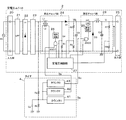
図3に示すように、定電流ユニット3は、入力部(接続部)30と、制御電源回路31と、DC−DC変換部32と、出力部(接続部)33と、定電流制御部34と、電流検出部35とを有する。   As shown in FIG. 3, the constant current unit 3 includes an input unit (connection unit) 30, a control power supply circuit 31, a DC-DC conversion unit 32, an output unit (connection unit) 33, and a constant current control unit 34. And a current detection unit 35.

入力部30は、定電圧ユニット2の出力部25からの出力電圧Vが定電流ユニット3への入力電圧Vとなって供給される。制御電源回路31は、定電圧ユニット2の制御電源回路23と同様の構成を成し、DC−DC変換部32、定電流制御部34、及び電流検出部35など、定電流ユニット3内の各回路に定電圧源Vccを供給する。   The input unit 30 is supplied with the output voltage V from the output unit 25 of the constant voltage unit 2 as the input voltage V to the constant current unit 3. The control power supply circuit 31 has the same configuration as the control power supply circuit 23 of the constant voltage unit 2, and includes a DC-DC conversion unit 32, a constant current control unit 34, a current detection unit 35, and the like in the constant current unit 3. A constant voltage source Vcc is supplied to the circuit.

DC−DC変換部32は、駆動回路36と、この駆動回路36により駆動されるスイッチング素子Q2と、駆動回路36への入力信号を切り換える論理和回路AND2と、回生用のダイオードD2と、チョークコイルL3と、コンデンサC2とを有する。スイッチング素子Q2はチョークコイルL3と直列回路を成して入力部30と出力部33間に接続される。ダイオードD2は、スイッチング素子Q2とチョークコイルL3との接続点と接地間に逆方向接続される。チョークコイルL3の出力側はコンデンサC2を介して接地される。コンデンサC2は、照明負荷5と電流検知用の抵抗R6との直列回路と並列に接続され、照明負荷5と抵抗R6の接続点は電流検出部35に接続され、抵抗R6の他端は接地されている。AND2は、カウンタ41からの動作開始信号Saと、定電流制御部34からの電流制御信号とが入力される。 The DC-DC converter 32 includes a drive circuit 36, a switching element Q2 driven by the drive circuit 36, an OR circuit AND2 for switching an input signal to the drive circuit 36, a regenerative diode D2, and a choke coil. L3 and a capacitor C2. The switching element Q2 forms a series circuit with the choke coil L3 and is connected between the input unit 30 and the output unit 33. The diode D2 is connected in the reverse direction between the connection point between the switching element Q2 and the choke coil L3 and the ground. The output side of the choke coil L3 is grounded via the capacitor C2. The capacitor C2 is connected in parallel with the series circuit of the illumination load 5 and the current detection resistor R6, the connection point between the illumination load 5 and the resistor R6 is connected to the current detection unit 35, and the other end of the resistor R6 is grounded. ing. The AND 2 receives the operation start signal Sa from the counter 41 and the current control signal from the constant current control unit 34.

このDC−DC変換部32は、降圧チョッパ回路を成し、定電流制御部34からの電流制御信号によりスイッチング素子Q2を高周波でスイッチングすることにより、入力電圧Vを照明負荷5に必要な電圧に変換し出力部33から出力し、照明負荷5を点灯する。   The DC-DC converter 32 forms a step-down chopper circuit, and switches the switching element Q2 at a high frequency by a current control signal from the constant current controller 34, whereby the input voltage V is changed to a voltage required for the lighting load 5. It converts and outputs from the output part 33, and the illumination load 5 is lighted.

AND2は、カウンタ41からの動作開始信号SaがHレベルのときは、定電流制御部34からのオン・オフ制御信号からなる電流制御信号をそのまま出力し、このオン・オフ制御信号を基に駆動回路36でスイッチング素子Q2を駆動し、DC−DC変換部32の定電流動作が維持される。また、AND2はカウンタ41からの動作開始信号SaがLレベルのときは、定電流制御部34からの電流制御信号に関わらず、その出力もLレベルとなる。このとき、駆動回路36へは電流制御信号が入力されないので、スイッチング素子Q2は動作しないため、DC−DC変換部32の定電流動作は、停止状態に維持される。   When the operation start signal Sa from the counter 41 is at the H level, the AND 2 outputs the current control signal composed of the on / off control signal from the constant current control unit 34 as it is, and is driven based on this on / off control signal. The switching element Q2 is driven by the circuit 36, and the constant current operation of the DC-DC converter 32 is maintained. Further, when the operation start signal Sa from the counter 41 is at the L level, the output of the AND 2 is also at the L level regardless of the current control signal from the constant current control unit 34. At this time, since the current control signal is not input to the drive circuit 36, the switching element Q2 does not operate. Therefore, the constant current operation of the DC-DC converter 32 is maintained in a stopped state.

電流検出部35は、照明負荷5の電流により抵抗R6に発生する電圧が入力されて、出力部33から照明負荷5に流れる出力電流を検出し、その検出値を定電流制御部34へ入力する。定電流制御部34は、この検出値を基にDC−DC変換部32から出力される電流Iが所望の一定値に保たれるように、スイッチング素子Q2をオン、オフ制御する。なお、電流検出部35は、増幅回路を含んでもよい。また、定電流制御部34からのオン・オフ制御信号のスイッチング周波数は数10KHzから数MHzである。   The current detection unit 35 receives the voltage generated in the resistor R6 due to the current of the lighting load 5, detects the output current flowing from the output unit 33 to the lighting load 5, and inputs the detected value to the constant current control unit 34. . The constant current control unit 34 controls the switching element Q2 on and off so that the current I output from the DC-DC conversion unit 32 is maintained at a desired constant value based on the detected value. The current detection unit 35 may include an amplifier circuit. The switching frequency of the on / off control signal from the constant current control unit 34 is several tens KHz to several MHz.

ここで、カウンタ41、42により制御される各ユニット2、3の動作時の電圧、電流波形について図4(a)〜(d)を参照して説明する。図4(a)は定電圧ユニット2の動作時におけるコンデンサC1の出力電圧Vの波形を、図4(b)は定電流ユニット3の動作時におけるコイルL3の出力電流Iの波形を示す。図4(c)はカウンタ41からの動作開始信号Saの波形を、図4(d)はカウンタ42からの動作開始信号Sbの波形を示す。前述のように、カウンタ41によって所望の経過時間が計時される時間(tc1)は、カウンタ42によって経過時間が計時される時間(tc2)より短く設定されるので、カウンタ41からの動作開始信号Saのオンする時間t2は、カウンタ42からの動作開始信号Sbのオンする時間t3より短くなっている。   Here, voltage and current waveforms during operation of the units 2 and 3 controlled by the counters 41 and 42 will be described with reference to FIGS. 4A shows the waveform of the output voltage V of the capacitor C1 when the constant voltage unit 2 is operating, and FIG. 4B shows the waveform of the output current I of the coil L3 when the constant current unit 3 is operating. 4C shows the waveform of the operation start signal Sa from the counter 41, and FIG. 4D shows the waveform of the operation start signal Sb from the counter. As described above, the time (tc1) for which the desired elapsed time is counted by the counter 41 is set shorter than the time (tc2) for which the elapsed time is counted by the counter 42. Therefore, the operation start signal Sa from the counter 41 is set. The turn-on time t2 is shorter than the turn-on time t3 of the operation start signal Sb from the counter 42.

図4(a)に示すように、定電圧ユニット2の出力電圧Vは、交流電源が投入された時間をt=0とすると、整流回路部22の出力が増加し、時間t1で交流電圧のピークの電圧V1まで上昇し、昇圧チョッパ部24が動作を開始する時間t3まで電圧V1が出力される。電圧V1はAC電源のピーク値電圧であり、AC100(V)の場合は、約141V程度である。ここでは、時間t1〜t3の期間に、定電圧制御部27及び駆動回路26は制御電源回路23から供給されており、カウンタ42からの動作開始信号Sbの発生により昇圧チョッパ部24がいつでも動作開始できるようにスタンバイされている。   As shown in FIG. 4A, the output voltage V of the constant voltage unit 2 increases the output of the rectifier circuit unit 22 when the time when the AC power is turned on is t = 0, and the AC voltage is increased at time t1. The voltage V1 rises to the peak voltage V1, and the voltage V1 is output until time t3 when the boost chopper 24 starts operation. The voltage V1 is a peak value voltage of the AC power supply. In the case of AC100 (V), it is about 141V. Here, the constant voltage control unit 27 and the drive circuit 26 are supplied from the control power supply circuit 23 during the period of time t1 to t3, and the boost chopper unit 24 starts to operate at any time by the generation of the operation start signal Sb from the counter 42. Be on standby to be able to.

時間t3〜t4の電圧Vは、時間t3から定電圧制御部27のチョッパ動作が開始することにより、出力電圧Vは昇圧チョッパ部24で昇圧されて電圧V1から、時間t4で予め定める一定電圧Voまで上昇する。時間t4以降は、定電圧制御部27のフィードバック制御により、定電圧ユニット2のコンデンサC1の出力電圧Vは一定電圧Voに維持される。   The voltage V from time t3 to t4 is increased by the chopper operation of the constant voltage control unit 27 from time t3, so that the output voltage V is boosted by the boosting chopper unit 24, and the voltage V1 is constant voltage Vo predetermined at time t4. To rise. After time t4, the output voltage V of the capacitor C1 of the constant voltage unit 2 is maintained at a constant voltage Vo by feedback control of the constant voltage control unit 27.

図4(b)に示すように、定電流ユニット3のDC−DC変換部32は、カウンタ41で定められた時間t2に達するまでは駆動しないため、チョークコイルL3に電流は流れない。ただし、時間t2に達するまでに、定電流制御部34および電流検出部35の制御電源は十分供給できる電圧に設定されているため、時間t2経過した点から、速やかに動作を開始できる。   As shown in FIG. 4B, the DC-DC converter 32 of the constant current unit 3 is not driven until the time t2 determined by the counter 41 is reached, so that no current flows through the choke coil L3. However, since the control power supply of the constant current control unit 34 and the current detection unit 35 is set to a voltage that can be sufficiently supplied by the time t2, the operation can be started immediately after the time t2 has elapsed.

時間t2〜t3において、定電流制御部34は出力電圧V1を電源として動作を開始する。このとき、定格電流よりは大きいピーク電流Ipeakが流れることになるが、この期間では、まだ定電圧ユニット2の昇圧チョッパ部24は動作を開始していないので、過電流により定電圧制御のフィードバック検出量が急激に大きくならない。従って、定電圧制御部27はその制御の許容量を超え、フィードバック制御が外れて回路動作が不能になることはなく、出力電流Iは電源電圧V1に応じた一定値Io1に収束する。   At time t2 to t3, the constant current control unit 34 starts operation using the output voltage V1 as a power source. At this time, a peak current Ipeak larger than the rated current flows. However, during this period, the boost chopper unit 24 of the constant voltage unit 2 has not yet started operation, and therefore, feedback detection of constant voltage control due to overcurrent. The amount does not increase rapidly. Therefore, the constant voltage control unit 27 does not exceed the control allowable amount, the feedback control is not lost and the circuit operation is not disabled, and the output current I converges to a constant value Io1 corresponding to the power supply voltage V1.

時間t3〜t4においては、時間t3で定電圧ユニット2の昇圧チョッパ部24が動作を開始するので、出力電圧Vの上昇に伴い、徐々に電流Iは減少していき、やがて所望の電流値Io2に維持される。時間t4以降は、定電流制御部34のフィードバック制御が継続されることになる。   From time t3 to t4, the step-up chopper unit 24 of the constant voltage unit 2 starts operating at time t3, so that the current I gradually decreases as the output voltage V increases, and eventually the desired current value Io2 Maintained. After time t4, the feedback control of the constant current control unit 34 is continued.

カウンタ41は、抵抗Rb端の電圧でタイマ動作を開始し、予め設定された経過時間に達する時間t2まではLレベルが維持される。カウンタ41は時間t2を経過すると、動作開始信号SaがHレベルになり、カウンタ42より早く始動する。この動作開始信号Saが定電流制御のAND2への入力されると、時間t2から定電流ユニット3のDC−DC変換部32が動作を開始することになり、出力電流Iが立ち上がる。   The counter 41 starts a timer operation with the voltage at the end of the resistor Rb, and maintains the L level until the time t2 when the preset elapsed time is reached. When the time t <b> 2 has elapsed, the operation start signal Sa becomes H level and the counter 41 starts earlier than the counter 42. When this operation start signal Sa is input to the constant current control AND2, the DC-DC converter 32 of the constant current unit 3 starts operating from time t2, and the output current I rises.

カウンタ42は、時間t2より長い経過時間の時間t3までは、Lレベルが維持され、時間t3経過すると、その動作開始信号SbがHレベルになる。この動作開始信号Sbが定電圧制御のAND1回路へ入力されると、時間t3から定電圧ユニット2の昇圧チョッパ部24が動作を開始し、出力電圧VがV1から昇圧され、Voに一定制御されるようになる。これにより、定電圧ユニット2の起動のタイミングは、定電流ユニット3の起動のタイミングから離されることになる。   The counter 42 is maintained at the L level until the time t3, which is an elapsed time longer than the time t2, and when the time t3 has elapsed, the operation start signal Sb becomes the H level. When this operation start signal Sb is input to the AND1 circuit for constant voltage control, the boost chopper unit 24 of the constant voltage unit 2 starts operating from time t3, the output voltage V is boosted from V1, and is controlled to be constant to Vo. Become so. Thereby, the start timing of the constant voltage unit 2 is separated from the start timing of the constant current unit 3.

本実施形態によれば、タイマ4を用いて、予め定められた一定時間(時間t3)を定電圧ユニット2が動作開始するまでの時間として、定電流ユニット3が一定時間前に動作開始するようにできる。従って、定電流ユニット3の動作開始時のピーク電流Ipeakによる過電流の影響により定電圧ユニット2の定電圧動作が停止されることを防止することができ、回路全体を起動することできる。   According to the present embodiment, the constant current unit 3 is started to operate a certain time before using the timer 4 as a time until the constant voltage unit 2 starts to operate for a predetermined time (time t3). Can be. Therefore, it is possible to prevent the constant voltage operation of the constant voltage unit 2 from being stopped due to the influence of the overcurrent due to the peak current Ipeak at the start of the operation of the constant current unit 3, and to start up the entire circuit.

また、複数のタイマ4(カウンタ41〜43)を有しているので、任意の経過時間後に各ユニット2、3を動作開始させることができる。これにより、各ユニット2、3内の制御回路の切替時に、出力電流Iの立ち上がりに振動波形が出るような場合は、その振動が収まる十分な安定時間を見てから定電圧ユニット2の昇圧チョッパ部24を動作開始させることができ、安定性が向上する。   Moreover, since the plurality of timers 4 (counters 41 to 43) are provided, the operations of the units 2 and 3 can be started after an arbitrary elapsed time. As a result, when a vibration waveform appears at the rise of the output current I when switching the control circuit in each unit 2, 3, the boost chopper of the constant voltage unit 2 is viewed after a sufficient stabilization time during which the vibration falls. The operation of the unit 24 can be started, and the stability is improved.

また、定電圧ユニット2内に、昇圧チョッパ部24と降圧チョッパ部28のように複数の定電圧回路が存在しても、定電流ユニット3の動作開始による過電流の影響を受けないように、各々の定電圧回路を適正な時間経過後に動作開始することができる。このとき、昇圧チョッパ部24を最後に動作するように設定することにより、昇圧チョッパ回路のフィードバック外れを防止することができる。   Further, even if there are a plurality of constant voltage circuits such as the step-up chopper unit 24 and the step-down chopper unit 28 in the constant voltage unit 2, the constant current unit 3 is not affected by overcurrent due to the start of operation of the constant current unit 3. The operation of each constant voltage circuit can be started after an appropriate time has elapsed. At this time, by setting the boost chopper unit 24 to operate last, it is possible to prevent the boost chopper circuit from coming off the feedback.

また、タイマ4による計測のスタートとして、定電圧ユニット2および定電流ユニット3とも、定電圧ユニット2の昇圧チョッパ部24への入力電圧の検出を基に行ったが、定電圧ユニット2の動作開始までの時間計測のスタートは、必ずしもこれに限ったものではない。例えば、定電流ユニット3が動作開始した信号やDC−DC変換部32の出力電流Iが一定値に収まってからなどの様々な信号で動作を開始することができる。ここでは、昇圧チョッパ部24の動作開始前にDC−DC変換部32が動作を開始し、定電圧ユニット2の起動時間を定電流ユニット3の起動時間より遅くらせるようにさえすればよい。   Further, as the start of measurement by the timer 4, both the constant voltage unit 2 and the constant current unit 3 are performed based on detection of the input voltage to the boost chopper unit 24 of the constant voltage unit 2, but the operation of the constant voltage unit 2 is started. The start of time measurement up to is not necessarily limited to this. For example, the operation can be started with various signals such as a signal that the constant current unit 3 has started to operate and the output current I of the DC-DC converter 32 has fallen to a constant value. Here, it is only necessary to start the operation of the DC-DC converter 32 before starting the operation of the step-up chopper 24 and delay the start-up time of the constant voltage unit 2 from the start-up time of the constant current unit 3.

なお、上記昇圧チョッパ部24の動作開始の時間計測を出力電流Iが一定値に収まってから設定する場合、例えば、時間t2〜t3での出力電流Io1(図4(b)参照)が一定値になるのを検出して、昇圧チョッパ部24の動作を開始すると、タイマ4での回路部品が少なく済むなどの利点を生じる。例えば、出力電流Iの検出は、電流検出部35に接続される電流検出用の抵抗R6を兼用すればよい。   When the time measurement for starting the operation of the step-up chopper unit 24 is set after the output current I falls within a constant value, for example, the output current Io1 (see FIG. 4B) at the time t2 to t3 is a constant value. When the operation of the step-up chopper unit 24 is started, there are advantages such as fewer circuit components in the timer 4. For example, the output current I may be detected by using the current detection resistor R 6 connected to the current detection unit 35.

(第1の実施形態の変形例)
次に、上記実施形態の変形例について、図5乃至図7を参照して説明する。この変形例においては、定電圧ユニット2は、図5に示すように、昇圧チョッパ部24の後段に、その出力を受けて降圧する降圧チョッパ部28を有し、降圧チョッパ部28からの直流電圧が出力部25から出力される。
(Modification of the first embodiment)
Next, a modification of the above embodiment will be described with reference to FIGS. In this modified example, the constant voltage unit 2 has a step-down chopper unit 28 that receives the output and steps down the step-down chopper unit 24 at the subsequent stage of the step-up chopper unit 24, as shown in FIG. Is output from the output unit 25.

図6に示すように、降圧チョッパ部28は前述の図3のDC−DC変換部32と同様の構成を成し、スイッチング素子Q3と、スイッチング素子Q3を駆動する駆動回路29と、論理和回路AND3と、ダイオードD3と、チョークコイルL4、電圧検出用の抵抗R7、R8の直列回路と、コンデンサC3とを備える。抵抗R7、R8の接続点の電圧は、定電圧制御部27にフィードバック入力され、コンデンサC3の電圧は定電圧制御部27により定電圧制御され、出力電圧Vとして出力部25から出力される。   As shown in FIG. 6, the step-down chopper 28 has the same configuration as the DC-DC converter 32 shown in FIG. 3, and includes a switching element Q3, a drive circuit 29 for driving the switching element Q3, and an OR circuit. The circuit includes an AND3, a diode D3, a choke coil L4, a series circuit of resistors R7 and R8 for voltage detection, and a capacitor C3. The voltage at the connection point of the resistors R7 and R8 is fed back to the constant voltage controller 27, and the voltage of the capacitor C3 is constant voltage controlled by the constant voltage controller 27 and output from the output unit 25 as the output voltage V.

AND3は、後述のカウンタ43からの動作開始信号Scと、定電圧制御部27により出力電圧Vをフィードバック制御するための他の電圧制御信号とが入力される。 The AND 3 receives an operation start signal Sc from a counter 43 (to be described later) and another voltage control signal for feedback control of the output voltage V by the constant voltage control unit 27 .

定電圧制御部27は、スイッチング素子Q3を一定の周波数、一定のオン時間でオン、オフすることにより、一定の比率で昇圧チョッパ部24からの電圧Vbを降圧し、出力電圧Vを出力部25から出力する。例えば、交流電源ACの入力電圧が100〜242(V)の場合、昇圧チョッパ部24の出力を400(V)程度にしておき、降圧チョッパ部28で24(V)や48(V)のような直流電圧にして、後段の定電流ユニット3で照明負荷5を点灯させることができる。 The constant voltage control unit 27 turns the switching element Q3 on and off at a constant frequency and a constant on-time, thereby stepping down the voltage Vb from the boost chopper unit 24 at a constant ratio and outputting the output voltage V to the output unit 25. Output from. For example, when the input voltage of the AC power supply AC is 100 to 242 (V), the output of the step-up chopper unit 24 is set to about 400 (V), and the step-down chopper unit 28 sets the output to 24 (V) or 48 (V). The lighting load 5 can be turned on by the constant current unit 3 in the subsequent stage with a direct current voltage.

タイマ4は、カウンタ41、42に加え、動作開始信号Scを出力するカウンタ43を、さらに備える。ここでは、カウンタ41、42、および43の各出力の動作開始信号Sa、動作開始信号Sb、動作開始信号Scは、それぞれ定電流ユニット3のAND2、定電圧ユニット2のAND1、AND3にそれぞれ入力される。   The timer 4 further includes a counter 43 that outputs an operation start signal Sc in addition to the counters 41 and 42. Here, the operation start signal Sa, the operation start signal Sb, and the operation start signal Sc of the outputs of the counters 41, 42, and 43 are respectively input to AND2 of the constant current unit 3 and AND1 and AND3 of the constant voltage unit 2. The

ここで、カウンタ41、42、及び43により制御される各ユニット2、3の動作時の電圧、電流波形について図7(a)〜(c)を参照して説明する。図7(a)は定電圧ユニット2における昇圧チョッパ部24の出力電圧Vbの波形を、図7(b)は定電圧ユニット2のコンデンサC3から出力される出力電圧Vの波形を、図7(c)は定電流ユニット3の動作時におけるコイルL3の出力電流Iの波形を示す。なお、図7(a)、(b)、(c)で時間軸は一致して表記してある。 Here, voltage and current waveforms during operation of the units 2 and 3 controlled by the counters 41, 42, and 43 will be described with reference to FIGS. 7A shows the waveform of the output voltage Vb of the step-up chopper unit 24 in the constant voltage unit 2, FIG. 7B shows the waveform of the output voltage V output from the capacitor C3 of the constant voltage unit 2, and FIG. c) shows the waveform of the output current I of the coil L3 when the constant current unit 3 is in operation. In FIGS. 7A, 7B, and 7C, the time axes are shown to coincide.

図7(a)に示すように、電源AC投入後、電圧Vbは電源電圧のピーク値であるVb1まで上昇する。ここで、タイマ4の制御により、動作開始信号Sc(時間t2でオン)、動作開始信号Sa(時間t3でオン)、動作開始信号Sb(時間t4でオン)の順で各AND2(図3)、AND3(図6)、AND1が動作を開始するようにする。このとき、後段の定電流ユニット3のDC−DC変換部32、定電流制御部34、電流検出部35を含む定電流回路部が動作開始する時間t3においては、図7(b)に示すように、降圧チョッパ部28のみが起動(時間t2でオン)している。このため、昇圧チョッパ部24の出力Vb1、降圧チョッパ部28の出力Vo1の電圧で定電流回路部が動作することになる。ここで、出力Vb1は昇圧チョッパ部24が停止しているので、整流回路部22の出力(約141V)と同じになる。   As shown in FIG. 7A, after the power supply AC is turned on, the voltage Vb rises to Vb1, which is the peak value of the power supply voltage. Here, under the control of the timer 4, each AND2 (FIG. 3) in the order of the operation start signal Sc (ON at time t2), the operation start signal Sa (ON at time t3), and the operation start signal Sb (ON at time t4). , AND3 (FIG. 6), and AND1 start operation. At this time, at a time t3 when the constant current circuit unit including the DC-DC conversion unit 32, the constant current control unit 34, and the current detection unit 35 of the subsequent constant current unit 3 starts operating, as shown in FIG. In addition, only the step-down chopper unit 28 is activated (turned on at time t2). For this reason, the constant current circuit unit operates with the voltage of the output Vb1 of the step-up chopper unit 24 and the output Vo1 of the step-down chopper unit 28. Here, since the step-up chopper unit 24 is stopped, the output Vb1 becomes the same as the output (about 141 V) of the rectifier circuit unit 22.

このような状態で、定電流ユニット3を起動させ、ピーク値Ipeakの大きい電流を流しておき、定電流ユニット3の出力電流Iが一定値Io1になった後、最後に昇圧チョッパ部24の動作を開始する。これにより、昇圧チョッパの出力はVb1からVb2へ上昇し、それに伴い、降圧チョッパ部28の出力もVo1からVo2へと上昇する。   In such a state, the constant current unit 3 is started, a current having a large peak value Ipeak is allowed to flow, and after the output current I of the constant current unit 3 reaches a constant value Io1, the operation of the boost chopper unit 24 is finally performed. To start. As a result, the output of the step-up chopper increases from Vb1 to Vb2, and accordingly, the output of the step-down chopper unit 28 also increases from Vo1 to Vo2.

これらの動作により、定電流ユニット3のDC−DC変換部32の出力電流はIo1からIo2へと減少して、定格点灯を維持することになる。このように動作させることにより、ピーク電流Ipeakによる昇圧チョッパ部24の停止を防止することができる。また、昇圧チョッパ部24の起動により、出力電流がIo1からIo2へ減少するため、回路ストレスが低減できる。   With these operations, the output current of the DC-DC converter 32 of the constant current unit 3 decreases from Io1 to Io2, and the rated lighting is maintained. By operating in this way, it is possible to prevent the boost chopper 24 from being stopped by the peak current Ipeak. In addition, since the output current decreases from Io1 to Io2 by starting up the boost chopper unit 24, circuit stress can be reduced.

(第2の実施形態)
本発明の第2の実施形態に係る過電流防止式電源装置について、図8及び図9を参照して説明する。本実施形態は、定電圧ユニット2内に調光部7aと調光信号送信部7bとを有し、定電流ユニット3内に、そのDC−DC変換部32の出力を受けて動作する調光出力部8を備える。調光出力部8は、定電圧ユニット2側からの調光信号S1によって制御され、照明負荷5を調光制御する。
(Second Embodiment)
An overcurrent prevention type power supply device according to a second embodiment of the present invention will be described with reference to FIGS. In the present embodiment, the constant voltage unit 2 has a dimmer 7a and a dimming signal transmitter 7b, and the constant current unit 3 operates by receiving the output of the DC-DC converter 32. An output unit 8 is provided. The dimming output unit 8 is controlled by the dimming signal S1 from the constant voltage unit 2 side, and performs dimming control on the illumination load 5.

図8に示すように、定電圧ユニット2において、調光部7a及び調光信号送信部7bは、汎用ICの組合せやマイコンなどで構成され、定電圧源Vccから給電されて動作し、調光信号送信部7bからの調光信号S1を出力部25から送出する。   As shown in FIG. 8, in the constant voltage unit 2, the dimming unit 7a and the dimming signal transmitting unit 7b are configured by a combination of general-purpose ICs, a microcomputer, and the like, and are operated by being supplied with power from the constant voltage source Vcc. The dimming signal S1 from the signal transmission unit 7b is transmitted from the output unit 25.

調光部7aは、外部からの調光要求を受けて調光指令値に変換し、この調光指令値に基く指令信号を調光信号送信部7bに送る。調光指令値は、例えば、ユーザが抵抗ボリュームを回すことによって抵抗値を可変し、その抵抗値に対応する電圧値をマイコンで発生して形成することができ、また、リモコンからの制御信号を受けて形成することもできる。   The dimming unit 7a receives a dimming request from the outside, converts it to a dimming command value, and sends a command signal based on the dimming command value to the dimming signal transmission unit 7b. The dimming command value can be formed, for example, by changing the resistance value by the user turning the resistance volume, generating a voltage value corresponding to the resistance value with a microcomputer, and generating a control signal from the remote controller. It can also be formed.

調光信号送信部7bは、調光部7aからの指令信号を受けて、それに基いてPWM信号などの調光信号S1を生成し、定電流ユニット3へ送出する。PWM信号は、12Vの振幅を成す1kHzのパルス信号とし、そのオン時間が少ないほど調光率を高くするようにしている。なお、定格出力を調光率100%とする場合の調光信号S1は、振幅可変信号としてもよい。また、有線や無線の通信手段で定電流ユニット3側に伝達する場合は、それぞれ対応する通信変換機能を設ければよい。   The dimming signal transmitter 7b receives the command signal from the dimmer 7a, generates a dimming signal S1 such as a PWM signal based on the command signal, and sends it to the constant current unit 3. The PWM signal is a 1 kHz pulse signal having an amplitude of 12 V, and the dimming rate is increased as the ON time is shorter. The dimming signal S1 when the rated output is a dimming rate of 100% may be a variable amplitude signal. Moreover, when transmitting to the constant current unit 3 side by a wired or wireless communication means, a corresponding communication conversion function may be provided.

図9に示すように、調光出力部8はスイッチング素子Q4と、スイッチング素子Q4を駆動する駆動回路81とを有し、スイッチング素子Q4はDC−DC変換部32の出力側と出力部33との間に直列に接続される。駆動回路81は調光信号送信部7bからの調光信号S1が入力され、この調光信号S1に基いてスイッチング素子Q4をオン、オフし、その出力は出力部33から照明負荷5に供給される。   As shown in FIG. 9, the dimming output unit 8 includes a switching element Q4 and a drive circuit 81 that drives the switching element Q4. The switching element Q4 includes the output side of the DC-DC conversion unit 32, the output unit 33, and the like. Are connected in series. The drive circuit 81 receives the dimming signal S1 from the dimming signal transmission unit 7b, turns on and off the switching element Q4 based on the dimming signal S1, and the output is supplied from the output unit 33 to the illumination load 5. The

本実施形態によれば、調光信号送信部7bからの調光信号S1に応じて、有機EL等の照明負荷5の電流を調整して所望のレベルに調光することができると共に、起動時の調光出力部8へのピーク電流が抑制され、調光出力部8の過電流による破損等を防止できる。   According to the present embodiment, according to the dimming signal S1 from the dimming signal transmitter 7b, the current of the lighting load 5 such as an organic EL can be adjusted and adjusted to a desired level, and at the time of startup The peak current to the dimming output unit 8 is suppressed, and the dimming output unit 8 can be prevented from being damaged due to overcurrent.

図10は、上記定電圧ユニット2(過電流防止式電源装置)と、定電圧ユニット2により給電される複数の灯具(照明負荷)6(6a、6b)と、定電圧ユニット2と灯具6を接続する接続部61と、を備えた照明器具の構成例を示す。灯具6は、接続部61と共に、発光素子(照明負荷)5aと、定電流ユニット3と、調光信号受信部9とを有し、コネクタ等よりなる接続部61を介して定電圧ユニット2の出力部と配線接続されている。定電圧ユニット2は、その出力部からの出力電圧Vと調光信号S1とが接地ライン(GND)を共通として灯具6に接続され、それぞれ灯具6内の定電流ユニット3と調光信号受信部9とに供給される。   FIG. 10 shows the constant voltage unit 2 (overcurrent prevention type power supply device), a plurality of lamps (illumination loads) 6 (6a, 6b) fed by the constant voltage unit 2, the constant voltage unit 2 and the lamp 6. The structural example of the lighting fixture provided with the connection part 61 to connect is shown. The lamp 6 has a light emitting element (illumination load) 5a, a constant current unit 3, and a dimming signal receiving unit 9 together with the connection unit 61, and the constant voltage unit 2 is connected via the connection unit 61 made of a connector or the like. It is connected to the output unit by wiring. In the constant voltage unit 2, the output voltage V from the output unit and the dimming signal S1 are connected to the lamp 6 with a common ground line (GND), and the constant current unit 3 and the dimming signal receiving unit in the lamp 6 are respectively connected. 9 and.

発光素子5aは、入力電流と光出力がほぼ比例の関係にある有機ELやLEDなどの一つまたは複数の固体発光素子から成る。調光信号受信部9は、定電圧ユニット2の調光信号送信部7bからの調光信号S1を受けて元の調光指令値を復元し、それを定電流ユニット3に伝える。定電流ユニット3は、調光機能を有し、調光信号受信部9からの指令値を受けて発光素子5aのPWM調光や振幅調光を行う。なお、調光信号受信部9は、定電流ユニット3内に設けてもよい。   The light emitting element 5a is composed of one or a plurality of solid light emitting elements such as an organic EL or LED in which an input current and a light output are in a substantially proportional relationship. The dimming signal receiving unit 9 receives the dimming signal S1 from the dimming signal transmission unit 7b of the constant voltage unit 2, restores the original dimming command value, and transmits it to the constant current unit 3. The constant current unit 3 has a dimming function and receives a command value from the dimming signal receiver 9 to perform PWM dimming and amplitude dimming of the light emitting element 5a. The dimming signal receiver 9 may be provided in the constant current unit 3.

この照明器具は、複数の灯具6が定電圧ユニット2に接続されるような場合においても、動作開始時に配線に流れる定電圧ユニット2からのピーク電流を抑制することができる。これにより、過電流による灯具6の回路素子等へのストレスを低減することができると共に、点灯動作後は、電源変動に強い、安定した照明が得られる。また、定電圧ユニット2と各接続部61間の配線により、灯具6と定電圧ユニット2間を任意の長さに調整できる。また、LEDや有機EL素子の発光素子5aを用いたので、面状薄型の照明器具が得られる。   Even when a plurality of lamps 6 are connected to the constant voltage unit 2, this lighting fixture can suppress the peak current from the constant voltage unit 2 flowing through the wiring at the start of operation. As a result, it is possible to reduce stress on the circuit elements and the like of the lamp 6 due to overcurrent, and after the lighting operation, stable illumination resistant to power supply fluctuations can be obtained. Further, the distance between the lamp 6 and the constant voltage unit 2 can be adjusted to an arbitrary length by the wiring between the constant voltage unit 2 and each connection portion 61. Moreover, since the light emitting element 5a of LED or an organic EL element was used, a planar thin luminaire can be obtained.

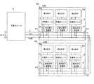
図11は、照明器具を複数のモジュールで構成した場合の例を示す。この照明器具は、定電圧ユニット2及び定電流ユニット3をモジュール化した電源ユニット(電源装置)1aと、複数の発光素子5aを一体にしてモジュール化した負荷モジュール5bとにより構成される。これらのモジュール化により、照明器具をコンパクトに形成でき、また、交換修理が容易になる。   FIG. 11 shows an example in which the lighting fixture is composed of a plurality of modules. This lighting fixture includes a power supply unit (power supply device) 1a obtained by modularizing the constant voltage unit 2 and the constant current unit 3, and a load module 5b obtained by modularizing a plurality of light emitting elements 5a. Due to these modularizations, the lighting fixture can be made compact, and replacement and repair can be facilitated.

なお、本発明は、上記実施形態の構成に限られず、発明の趣旨を変更しない範囲で種々の変形が可能である。例えば、上記各実施形態において、定電圧ユニット2内に降圧チョッパ部28を複数設け、タイマ4のカウンタを3個以上設けて各チョッパ回路の動作開始を時間シフトさせてもよい。また、スイッチング素子はFETに限らず、バイポーラトランジスタ等、他の半導体素子を用いてもよい。また、1つの電源装置1に照明負荷5を複数接続するときは、それらの照明負荷5の直列、並列、あるいはそれらの組合せであってもよい。また、電流検出に抵抗を用いたが、トランスなどを用いてもよい。   In addition, this invention is not restricted to the structure of the said embodiment, A various deformation | transformation is possible in the range which does not change the meaning of invention. For example, in each of the above-described embodiments, a plurality of step-down chopper units 28 may be provided in the constant voltage unit 2 and three or more counters of the timer 4 may be provided to time-shift the operation start of each chopper circuit. The switching element is not limited to the FET, and other semiconductor elements such as a bipolar transistor may be used. When a plurality of lighting loads 5 are connected to one power supply device 1, the lighting loads 5 may be connected in series, in parallel, or a combination thereof. Further, although a resistor is used for current detection, a transformer or the like may be used.

1 電源装置(過電流防止式電源装置、照明器具)
2 定電圧ユニット
3 定電流ユニット
24 昇圧チョッパ部(昇圧チョッパ回路)
27 定電圧制御部(制御回路)
4 タイマ
41、42、43 カウンタ(タイマ)
5 照明負荷
5a 発光素子(照明負荷、照明器具)
6、6a、6b 灯具(照明器具)
61 接続部(照明器具)
Sa、Sb、Sc 動作開始信号(信号)
1 Power supply (overcurrent prevention power supply, lighting equipment)
2 Constant voltage unit 3 Constant current unit 24 Boost chopper (boost chopper circuit)
27 Constant voltage controller (control circuit)
4 Timer 41, 42, 43 Counter (Timer)
5 Lighting load 5a Light emitting element (lighting load, lighting fixture)
6, 6a, 6b Lamp (lighting fixture)
61 Connection (lighting fixture)
Sa, Sb, Sc Operation start signal (signal)

Claims (4)

一定電圧を出力する定電圧ユニットと、
前記定電圧ユニットからの電圧を受けて駆動される定電流ユニットと、
前記定電圧ユニットへの電圧供給開始後の経過時間を計測するためのタイマと、を備え、
前記定電流ユニットは、前記タイマにより計測される経過時間が予め定められた一定時間を経過する前に動作を開始することを特徴とする過電流防止式電源装置。
A constant voltage unit that outputs a constant voltage;
A constant current unit driven by receiving a voltage from the constant voltage unit;
A timer for measuring an elapsed time after the start of voltage supply to the constant voltage unit,
The overcurrent prevention type power supply device, wherein the constant current unit starts an operation before an elapsed time measured by the timer elapses a predetermined time.
前記タイマを複数有し、
前記タイマは、前記定電流ユニットと定電圧ユニットとに、それぞれ動作開始のための信号を伝達することを特徴とする請求項1に記載の過電流防止式電源装置。
A plurality of the timers;
The timer, before the Kijo current unit and a constant voltage unit, load determination device of claim 1, wherein the transmitting a signal for each operation start.
前記定電圧ユニットは、入力電圧を昇圧する昇圧チョッパ回路と、該昇圧チョッパ回路を駆動するための制御回路とを有し、
前記予め設定された一定時間は、前記昇圧チョッパ回路の制御回路が動作を開始するまでの時間よりも短いことを特徴とする請求項1または請求項2に記載の過電流防止式電源装置。
The constant voltage unit includes a boost chopper circuit that boosts an input voltage, and a control circuit for driving the boost chopper circuit,
3. The overcurrent prevention type power supply device according to claim 1, wherein the predetermined time is shorter than a time until the control circuit of the step-up chopper circuit starts to operate.
請求項1乃至請求項3のいずれか一項に記載の過電流防止式電源装置と、照明負荷と、前記電源装置と照明負荷とを接続する接続部と、を備えたことを特徴とする照明器具。   The overcurrent prevention type power supply device according to any one of claims 1 to 3, an illumination load, and a connection portion that connects the power supply device and the illumination load. Instruments.
JP2010073509A 2010-03-26 2010-03-26 Overcurrent prevention type power supply device and lighting fixture using the same Expired - Fee Related JP5579477B2 (en)

Priority Applications (1)

Application Number Priority Date Filing Date Title
JP2010073509A JP5579477B2 (en) 2010-03-26 2010-03-26 Overcurrent prevention type power supply device and lighting fixture using the same

Applications Claiming Priority (1)

Application Number Priority Date Filing Date Title
JP2010073509A JP5579477B2 (en) 2010-03-26 2010-03-26 Overcurrent prevention type power supply device and lighting fixture using the same

Publications (2)

Publication Number Publication Date
JP2011205868A JP2011205868A (en) 2011-10-13
JP5579477B2 true JP5579477B2 (en) 2014-08-27

Family

ID=44881878

Family Applications (1)

Application Number Title Priority Date Filing Date
JP2010073509A Expired - Fee Related JP5579477B2 (en) 2010-03-26 2010-03-26 Overcurrent prevention type power supply device and lighting fixture using the same

Country Status (1)

Country Link
JP (1) JP5579477B2 (en)

Cited By (1)

* Cited by examiner, † Cited by third party
Publication number Priority date Publication date Assignee Title
CN103327676A (en) * 2012-03-23 2013-09-25 台达电子工业股份有限公司 Power supply system and current control method thereof

Families Citing this family (13)

* Cited by examiner, † Cited by third party
Publication number Priority date Publication date Assignee Title
JP5554108B2 (en) * 2010-03-26 2014-07-23 パナソニック株式会社 Overcurrent prevention type power supply device and lighting fixture using the same
JP5962946B2 (en) * 2011-11-21 2016-08-03 パナソニックIpマネジメント株式会社 LIGHT EMITTING ELEMENT LIGHTING DEVICE AND LIGHTING DEVICE HAVING THE CIRCUIT
TWI496407B (en) 2012-03-23 2015-08-11 Delta Electronics Inc Power supply system and method of controlling current thereof
WO2013164891A1 (en) * 2012-05-02 2013-11-07 パイオニア株式会社 Light-emitting device
JP5991614B2 (en) * 2012-07-12 2016-09-14 パナソニックIpマネジメント株式会社 Light emitting element lighting device and lighting apparatus using the same
JP6131511B2 (en) * 2012-10-10 2017-05-24 パナソニックIpマネジメント株式会社 Lighting device and lighting apparatus using the same
JP2015076288A (en) * 2013-10-09 2015-04-20 パナソニックIpマネジメント株式会社 Lighting device and lighting fixture
JP6273642B2 (en) * 2013-12-16 2018-02-07 パナソニックIpマネジメント株式会社 LED lighting device
JP6344045B2 (en) * 2014-05-14 2018-06-20 岩崎電気株式会社 LED lighting circuit and LED lighting device
US9265116B2 (en) * 2014-05-30 2016-02-16 Technical Consumer Products, Inc. Constant voltage and constant current driver circuit
JP6613817B2 (en) * 2015-10-30 2019-12-04 三菱電機株式会社 Lighting device and lighting apparatus
JP7103130B2 (en) * 2018-09-28 2022-07-20 東芝ライテック株式会社 How to update the constant current regulator
JP7199011B2 (en) * 2018-11-30 2023-01-05 パナソニックIpマネジメント株式会社 load controller

Family Cites Families (7)

* Cited by examiner, † Cited by third party
Publication number Priority date Publication date Assignee Title
JPH05115172A (en) * 1991-10-21 1993-05-07 Fuji Electric Co Ltd Switching power supply starting circuit
JPH07142181A (en) * 1993-11-22 1995-06-02 Matsushita Electric Works Ltd Discharge lamp lighting device
JP3627573B2 (en) * 1999-05-13 2005-03-09 富士ゼロックス株式会社 Power supply
JP3647380B2 (en) * 2001-03-22 2005-05-11 シンクレイヤ株式会社 Constant voltage power supply device and transmission system relay device using the same
JP4825160B2 (en) * 2007-04-06 2011-11-30 コイズミ照明株式会社 LED lighting fixtures
JP5144194B2 (en) * 2007-09-25 2013-02-13 パナソニック株式会社 Lighting device and lighting apparatus
JP5554108B2 (en) * 2010-03-26 2014-07-23 パナソニック株式会社 Overcurrent prevention type power supply device and lighting fixture using the same

Cited By (1)

* Cited by examiner, † Cited by third party
Publication number Priority date Publication date Assignee Title
CN103327676A (en) * 2012-03-23 2013-09-25 台达电子工业股份有限公司 Power supply system and current control method thereof

Also Published As

Publication number Publication date
JP2011205868A (en) 2011-10-13

Similar Documents

Publication Publication Date Title
JP5579477B2 (en) Overcurrent prevention type power supply device and lighting fixture using the same
JP5554108B2 (en) Overcurrent prevention type power supply device and lighting fixture using the same
US8680775B2 (en) Lighting driver circuit and light fixture
TWI388115B (en) Power conversion drive circuit and lamp drive circuit
TWI436689B (en) Lighting apparatus and control method thereof
TWI508613B (en) High efficiency LED driver circuit and its driving method
TWI434603B (en) Led driving circuit and control circuit
US8749171B2 (en) Lighting apparatus and control method thereof
US20130038242A1 (en) Bias voltage generation using a load in series with a switch
JP6430665B2 (en) LED driver and driving method
TW201301936A (en) A cascade boost and inverting buck converter with independent control
JP6403042B2 (en) Power supply apparatus and lighting apparatus using the same
TWI445440B (en) Driving circuit
JP2011054538A (en) Led lighting device and illumination apparatus
KR20110095639A (en) Led lamp module
US20110266975A1 (en) Illumination controller and illumination driving system
US20130076257A1 (en) Switching mode pulsed current supply for driving leds
US9621060B2 (en) Self-excited power conversion circuit for secondary side control output power
JP6108143B2 (en) Overcurrent prevention type power supply device and lighting fixture using the same
CN102752906B (en) Lighting device and illumination apparatus having the same
US20130342121A1 (en) Luminaire
US9723668B2 (en) Switching converter and lighting device using the same
TW201401743A (en) Constant current control buck converter without current sense
US20110012537A1 (en) Driver circuit and method for driving load circuit
KR101472824B1 (en) Power supply unit for led lighting fixtures

Legal Events

Date Code Title Description
A711 Notification of change in applicant

Free format text: JAPANESE INTERMEDIATE CODE: A712

Effective date: 20120117

A621 Written request for application examination

Free format text: JAPANESE INTERMEDIATE CODE: A621

Effective date: 20121114

A977 Report on retrieval

Free format text: JAPANESE INTERMEDIATE CODE: A971007

Effective date: 20131113

A131 Notification of reasons for refusal

Free format text: JAPANESE INTERMEDIATE CODE: A131

Effective date: 20131119

A521 Request for written amendment filed

Free format text: JAPANESE INTERMEDIATE CODE: A523

Effective date: 20140117

TRDD Decision of grant or rejection written
A01 Written decision to grant a patent or to grant a registration (utility model)

Free format text: JAPANESE INTERMEDIATE CODE: A01

Effective date: 20140701

A61 First payment of annual fees (during grant procedure)

Free format text: JAPANESE INTERMEDIATE CODE: A61

Effective date: 20140709

R151 Written notification of patent or utility model registration

Ref document number: 5579477

Country of ref document: JP

Free format text: JAPANESE INTERMEDIATE CODE: R151

LAPS Cancellation because of no payment of annual fees