JP5541732B2 - Method for manufacturing liquid discharge head and method for manufacturing discharge port member - Google Patents
Method for manufacturing liquid discharge head and method for manufacturing discharge port member Download PDFInfo
- Publication number
- JP5541732B2 JP5541732B2 JP2010263680A JP2010263680A JP5541732B2 JP 5541732 B2 JP5541732 B2 JP 5541732B2 JP 2010263680 A JP2010263680 A JP 2010263680A JP 2010263680 A JP2010263680 A JP 2010263680A JP 5541732 B2 JP5541732 B2 JP 5541732B2
- Authority
- JP
- Japan
- Prior art keywords
- mask
- discharge port
- layer
- plating
- port member
- Prior art date
- Legal status (The legal status is an assumption and is not a legal conclusion. Google has not performed a legal analysis and makes no representation as to the accuracy of the status listed.)
- Expired - Fee Related
Links
- 238000000034 method Methods 0.000 title claims description 57
- 239000007788 liquid Substances 0.000 title claims description 41
- 238000004519 manufacturing process Methods 0.000 title claims description 26
- 238000007747 plating Methods 0.000 claims description 79
- 239000000758 substrate Substances 0.000 claims description 54
- 229910004298 SiO 2 Inorganic materials 0.000 claims description 17
- 238000007599 discharging Methods 0.000 claims description 6
- 238000002360 preparation method Methods 0.000 claims 1
- 239000000463 material Substances 0.000 description 52
- PXHVJJICTQNCMI-UHFFFAOYSA-N Nickel Chemical compound [Ni] PXHVJJICTQNCMI-UHFFFAOYSA-N 0.000 description 23
- 239000011347 resin Substances 0.000 description 18
- 229920005989 resin Polymers 0.000 description 18
- 238000005323 electroforming Methods 0.000 description 15
- 239000010408 film Substances 0.000 description 11
- 229910052759 nickel Inorganic materials 0.000 description 10
- 238000010586 diagram Methods 0.000 description 8
- 239000002585 base Substances 0.000 description 7
- URQUNWYOBNUYJQ-UHFFFAOYSA-N diazonaphthoquinone Chemical compound C1=CC=C2C(=O)C(=[N]=[N])C=CC2=C1 URQUNWYOBNUYJQ-UHFFFAOYSA-N 0.000 description 5
- 229920003229 poly(methyl methacrylate) Polymers 0.000 description 5
- 239000004926 polymethyl methacrylate Substances 0.000 description 5
- 239000002904 solvent Substances 0.000 description 5
- 238000009713 electroplating Methods 0.000 description 4
- XEEYBQQBJWHFJM-UHFFFAOYSA-N Iron Chemical compound [Fe] XEEYBQQBJWHFJM-UHFFFAOYSA-N 0.000 description 3
- 239000000853 adhesive Substances 0.000 description 3
- 230000001070 adhesive effect Effects 0.000 description 3
- 239000003513 alkali Substances 0.000 description 3
- 230000015572 biosynthetic process Effects 0.000 description 3
- 229910052751 metal Inorganic materials 0.000 description 3
- 239000002184 metal Substances 0.000 description 3
- 238000004544 sputter deposition Methods 0.000 description 3
- WQMWHMMJVJNCAL-UHFFFAOYSA-N 2,4-dimethylpenta-1,4-dien-3-one Chemical compound CC(=C)C(=O)C(C)=C WQMWHMMJVJNCAL-UHFFFAOYSA-N 0.000 description 2
- -1 Si 3 N 4 Inorganic materials 0.000 description 2
- 229910052804 chromium Inorganic materials 0.000 description 2
- 239000011651 chromium Substances 0.000 description 2
- 229910052802 copper Inorganic materials 0.000 description 2
- 239000010949 copper Substances 0.000 description 2
- JHIVVAPYMSGYDF-UHFFFAOYSA-N cyclohexanone Chemical compound O=C1CCCCC1 JHIVVAPYMSGYDF-UHFFFAOYSA-N 0.000 description 2
- 239000003822 epoxy resin Substances 0.000 description 2
- 239000011521 glass Substances 0.000 description 2
- 229910052737 gold Inorganic materials 0.000 description 2
- 238000010438 heat treatment Methods 0.000 description 2
- 229910010272 inorganic material Inorganic materials 0.000 description 2
- 239000011147 inorganic material Substances 0.000 description 2
- 239000011810 insulating material Substances 0.000 description 2
- 229910052742 iron Inorganic materials 0.000 description 2
- 230000005499 meniscus Effects 0.000 description 2
- KERTUBUCQCSNJU-UHFFFAOYSA-L nickel(2+);disulfamate Chemical compound [Ni+2].NS([O-])(=O)=O.NS([O-])(=O)=O KERTUBUCQCSNJU-UHFFFAOYSA-L 0.000 description 2
- 229910052763 palladium Inorganic materials 0.000 description 2
- 238000000059 patterning Methods 0.000 description 2
- 229920000647 polyepoxide Polymers 0.000 description 2
- 239000000565 sealant Substances 0.000 description 2
- WGTYBPLFGIVFAS-UHFFFAOYSA-M tetramethylammonium hydroxide Chemical compound [OH-].C[N+](C)(C)C WGTYBPLFGIVFAS-UHFFFAOYSA-M 0.000 description 2
- 239000010409 thin film Substances 0.000 description 2
- 239000004925 Acrylic resin Substances 0.000 description 1
- 229920000178 Acrylic resin Polymers 0.000 description 1
- 229910018072 Al 2 O 3 Inorganic materials 0.000 description 1
- VYZAMTAEIAYCRO-UHFFFAOYSA-N Chromium Chemical compound [Cr] VYZAMTAEIAYCRO-UHFFFAOYSA-N 0.000 description 1
- RYGMFSIKBFXOCR-UHFFFAOYSA-N Copper Chemical compound [Cu] RYGMFSIKBFXOCR-UHFFFAOYSA-N 0.000 description 1
- 238000000018 DNA microarray Methods 0.000 description 1
- 239000004593 Epoxy Substances 0.000 description 1
- NTIZESTWPVYFNL-UHFFFAOYSA-N Methyl isobutyl ketone Chemical compound CC(C)CC(C)=O NTIZESTWPVYFNL-UHFFFAOYSA-N 0.000 description 1
- UIHCLUNTQKBZGK-UHFFFAOYSA-N Methyl isobutyl ketone Natural products CCC(C)C(C)=O UIHCLUNTQKBZGK-UHFFFAOYSA-N 0.000 description 1
- 239000004809 Teflon Substances 0.000 description 1
- 229920006362 Teflon® Polymers 0.000 description 1
- 239000000919 ceramic Substances 0.000 description 1
- 239000002131 composite material Substances 0.000 description 1
- 230000008878 coupling Effects 0.000 description 1
- 238000010168 coupling process Methods 0.000 description 1
- 238000005859 coupling reaction Methods 0.000 description 1
- 230000007423 decrease Effects 0.000 description 1
- 238000005553 drilling Methods 0.000 description 1
- 238000001035 drying Methods 0.000 description 1
- 238000009429 electrical wiring Methods 0.000 description 1
- 238000007772 electroless plating Methods 0.000 description 1
- 238000005530 etching Methods 0.000 description 1
- 229910052732 germanium Inorganic materials 0.000 description 1
- 239000010931 gold Substances 0.000 description 1
- 229910052735 hafnium Inorganic materials 0.000 description 1
- XQBYLOYJNLQCLU-UHFFFAOYSA-N hepta-2,5-dien-4-one Chemical compound CC=CC(=O)C=CC XQBYLOYJNLQCLU-UHFFFAOYSA-N 0.000 description 1
- 238000007733 ion plating Methods 0.000 description 1
- 229910052741 iridium Inorganic materials 0.000 description 1
- 125000001449 isopropyl group Chemical group [H]C([H])([H])C([H])(*)C([H])([H])[H] 0.000 description 1
- 229910052748 manganese Inorganic materials 0.000 description 1
- 125000005397 methacrylic acid ester group Chemical group 0.000 description 1
- 229910052750 molybdenum Inorganic materials 0.000 description 1
- ORQBXQOJMQIAOY-UHFFFAOYSA-N nobelium Chemical compound [No] ORQBXQOJMQIAOY-UHFFFAOYSA-N 0.000 description 1
- KDLHZDBZIXYQEI-UHFFFAOYSA-N palladium Substances [Pd] KDLHZDBZIXYQEI-UHFFFAOYSA-N 0.000 description 1
- 238000000206 photolithography Methods 0.000 description 1
- 229910052697 platinum Inorganic materials 0.000 description 1
- 229920001721 polyimide Polymers 0.000 description 1
- 239000009719 polyimide resin Substances 0.000 description 1
- 229910052702 rhenium Inorganic materials 0.000 description 1
- 229910052707 ruthenium Inorganic materials 0.000 description 1
- 229910052709 silver Inorganic materials 0.000 description 1
- 229910052713 technetium Inorganic materials 0.000 description 1
- 229910052719 titanium Inorganic materials 0.000 description 1
- 229910052721 tungsten Inorganic materials 0.000 description 1
- 229910052720 vanadium Inorganic materials 0.000 description 1
- 238000007740 vapor deposition Methods 0.000 description 1
- 229910052726 zirconium Inorganic materials 0.000 description 1
Images


Classifications
-
- B—PERFORMING OPERATIONS; TRANSPORTING
- B41—PRINTING; LINING MACHINES; TYPEWRITERS; STAMPS
- B41J—TYPEWRITERS; SELECTIVE PRINTING MECHANISMS, i.e. MECHANISMS PRINTING OTHERWISE THAN FROM A FORME; CORRECTION OF TYPOGRAPHICAL ERRORS
- B41J2/00—Typewriters or selective printing mechanisms characterised by the printing or marking process for which they are designed
- B41J2/005—Typewriters or selective printing mechanisms characterised by the printing or marking process for which they are designed characterised by bringing liquid or particles selectively into contact with a printing material
- B41J2/01—Ink jet
- B41J2/135—Nozzles
- B41J2/16—Production of nozzles
- B41J2/1601—Production of bubble jet print heads
- B41J2/1603—Production of bubble jet print heads of the front shooter type
-
- B—PERFORMING OPERATIONS; TRANSPORTING
- B41—PRINTING; LINING MACHINES; TYPEWRITERS; STAMPS
- B41J—TYPEWRITERS; SELECTIVE PRINTING MECHANISMS, i.e. MECHANISMS PRINTING OTHERWISE THAN FROM A FORME; CORRECTION OF TYPOGRAPHICAL ERRORS
- B41J2/00—Typewriters or selective printing mechanisms characterised by the printing or marking process for which they are designed
- B41J2/005—Typewriters or selective printing mechanisms characterised by the printing or marking process for which they are designed characterised by bringing liquid or particles selectively into contact with a printing material
- B41J2/01—Ink jet
- B41J2/135—Nozzles
- B41J2/16—Production of nozzles
- B41J2/1621—Manufacturing processes
- B41J2/1631—Manufacturing processes photolithography
-
- B—PERFORMING OPERATIONS; TRANSPORTING
- B41—PRINTING; LINING MACHINES; TYPEWRITERS; STAMPS
- B41J—TYPEWRITERS; SELECTIVE PRINTING MECHANISMS, i.e. MECHANISMS PRINTING OTHERWISE THAN FROM A FORME; CORRECTION OF TYPOGRAPHICAL ERRORS
- B41J2/00—Typewriters or selective printing mechanisms characterised by the printing or marking process for which they are designed
- B41J2/005—Typewriters or selective printing mechanisms characterised by the printing or marking process for which they are designed characterised by bringing liquid or particles selectively into contact with a printing material
- B41J2/01—Ink jet
- B41J2/135—Nozzles
- B41J2/16—Production of nozzles
- B41J2/1621—Manufacturing processes
- B41J2/164—Manufacturing processes thin film formation
- B41J2/1643—Manufacturing processes thin film formation thin film formation by plating
-
- B—PERFORMING OPERATIONS; TRANSPORTING
- B41—PRINTING; LINING MACHINES; TYPEWRITERS; STAMPS
- B41J—TYPEWRITERS; SELECTIVE PRINTING MECHANISMS, i.e. MECHANISMS PRINTING OTHERWISE THAN FROM A FORME; CORRECTION OF TYPOGRAPHICAL ERRORS
- B41J2/00—Typewriters or selective printing mechanisms characterised by the printing or marking process for which they are designed
- B41J2/005—Typewriters or selective printing mechanisms characterised by the printing or marking process for which they are designed characterised by bringing liquid or particles selectively into contact with a printing material
- B41J2/01—Ink jet
- B41J2/135—Nozzles
- B41J2/16—Production of nozzles
- B41J2/1621—Manufacturing processes
- B41J2/164—Manufacturing processes thin film formation
- B41J2/1646—Manufacturing processes thin film formation thin film formation by sputtering
-
- Y—GENERAL TAGGING OF NEW TECHNOLOGICAL DEVELOPMENTS; GENERAL TAGGING OF CROSS-SECTIONAL TECHNOLOGIES SPANNING OVER SEVERAL SECTIONS OF THE IPC; TECHNICAL SUBJECTS COVERED BY FORMER USPC CROSS-REFERENCE ART COLLECTIONS [XRACs] AND DIGESTS
- Y10—TECHNICAL SUBJECTS COVERED BY FORMER USPC
- Y10T—TECHNICAL SUBJECTS COVERED BY FORMER US CLASSIFICATION
- Y10T29/00—Metal working
- Y10T29/49—Method of mechanical manufacture
- Y10T29/49401—Fluid pattern dispersing device making, e.g., ink jet
Description
本発明は、液体を吐出する吐出口を有する液体吐出ヘッドの製造方法と液体吐出ヘッド用の吐出口部材の製造方法に関する。 The present invention relates to a method for manufacturing a liquid discharge head having a discharge port for discharging a liquid and a method for manufacturing a discharge port member for a liquid discharge head.
液体吐出ヘッドはインクジェットプリンタに搭載されるインクジェットヘッドとして利用できる。特許文献1には、インクの吐出口が設けられた吐出口を有し、インクジェットプリンタに使用される吐出口部材を電鋳法によって形成する方法が開示されている。
The liquid discharge head can be used as an ink jet head mounted on an ink jet printer.
電鋳法を使用した吐出口部材の形成方法について詳しく説明する。図11は、液体吐出ヘッド1における吐出口及び液流路の部分の断面拡大図である。吐出口部材11は、吐出口12が複数個設けられており、接着剤16によって流路壁13に固定されている。流路壁13は、インクを吐出するためのエネルギーを発生するエネルギー発生素子14を有する素子基板10上に配置されている。流路壁13、素子基板10、及び吐出口部材11で囲まれた領域である液室にはインクが充填されている。そして、エネルギー発生素子14が発するエネルギーによって液室内のインクはインク滴になって吐出口部材11の吐出口12から飛翔し、印字用紙に付着する。
A method of forming the discharge port member using the electroforming method will be described in detail. FIG. 11 is an enlarged cross-sectional view of a portion of the discharge port and the liquid flow path in the
吐出口部材11に吐出口12を形成する方法は多数あり、例えば、ドリル加工、放電加工、レーザ加工、電鋳法等が一般に知られている。これらのうち、電鋳法は複数個の吐出口12を低コストで形成できる利点がある。
There are many methods for forming the
図4は、電鋳法により吐出口12を形成する一例を説明するための図である。まず、図4(a)に示すように、導電性の基体(導電性基板とも称す)21に感光性樹脂からなるレジスト17をコーティングする。次に、このレジスト17の上に開口を有するマスク18を配置する。なお、マスク18において、開口とそれに隣接する開口との距離(図4(a)矢印部分)はDである。そして、露光光19を用いて、この開口部分のレジスト17を露光する。これを現像処理すると、図4(b)に示すようにレジスト17は現像される。なお、レジスト17の厚さをtDとする。次に、導電性基板21に、電鋳法にてニッケル(Ni)をメッキすると、図4(c)に示すように、ニッケルメッキ20が積層される。この際、ニッケルメッキ20の間に、径dの吐出口が形成される。ニッケルメッキ20の厚さ(図4(c)参照)をtNとすると、径dはほぼ次式で表される。
FIG. 4 is a diagram for explaining an example of forming the
d≒D−2(tN−tD) ・・・・・・(式1)
したがって、dは、マスクにおける開口とそれに隣接する開口との間隔D、レジスト17の厚さtD、及びニッケルメッキ20の厚さtNによって決定される。tDは無視できる程度であるため、dを変化させない場合、吐出口同士の間隔を小さくしようとすると、メッキ厚さは小さくならざるを得ない。言い換えれば吐出口を高密度化するほど吐出口部材が薄くなる。
d≈D-2 (tN-tD) (Equation 1)
Therefore, d is determined by the distance D between the opening in the mask and the opening adjacent thereto, the thickness tD of the
ここで、メッキにより形成された吐出口部材の吐出口12に至る流路は、その径が吐出口12に向かって徐々に小さくなるように曲面で形成されている。吐出口部材がこのような形状でその厚さが薄く形成されると、吐出液滴を基板101に対して直進する方向に飛翔させるようにすることが困難となる。
Here, the flow path reaching the
そこで、本発明の目的は、電鋳法を用いて、高い吐出性能を有する吐出口部材を効率的に製造する方法を提供することである。 Then, the objective of this invention is providing the method of manufacturing efficiently the discharge outlet member which has high discharge performance using an electroforming method.
本発明は、
液体を吐出するために利用されるエネルギーを発生するエネルギー発生素子を備えた基板と、液体を吐出する吐出口が設けられ、前記基板と接合されることで前記吐出口と連通する液体の流路を形成する吐出口部材と、を有する液体吐出ヘッドの製造方法であって、
(1)前記吐出口を形成するための絶縁性の第1のマスクと、絶縁性の第2のマスクと、がこの順に積層された導電性の基体を用意する工程と、
(2)前記第1のマスクと前記第2のマスクとをマスクとして利用してメッキを行い第1のメッキ層の上面の前記基体からの高さが、第1のマスクの上面の前記基体からの高さより高く、第2のマスクの上面の前記基体からの高さより低くなるように、前記第1のメッキ層を形成する工程と、
(3)前記第2のマスクを除去する工程と、
(4)前記第1のマスクをマスクとして利用して前記基体にメッキを行うことにより、第2のメッキ層を第1のメッキ層を覆うように形成する工程と、
(5)前記基体と前記第1のマスクとを除去することにより前記吐出口部材を形成する工程と、
をこの順に有する液体吐出ヘッドの製造方法である。
The present invention
A liquid passage that is provided with a substrate including an energy generating element that generates energy used for discharging a liquid, and a discharge port that discharges the liquid, and communicates with the discharge port by being joined to the substrate. A discharge port member for forming a liquid discharge head comprising:
(1) preparing a conductive substrate in which an insulating first mask for forming the discharge port and an insulating second mask are laminated in this order;
(2) Plating is performed by using the first mask and the second mask as a mask, and the height of the upper surface of the first plating layer from the base is from the base of the upper surface of the first mask. Forming the first plating layer so as to be higher than the height of the second mask and lower than the height of the upper surface of the second mask from the substrate;
(3) removing the second mask;
(4) forming a second plating layer so as to cover the first plating layer by plating the base using the first mask as a mask;
(5) forming the discharge port member by removing the base and the first mask;
In this order.
また、本発明は、
液体を吐出する液体吐出ヘッドに用いられる、前記吐出口が設けられた吐出口部材の製造方法であって、
(1)前記吐出口を形成するための絶縁性の第1のマスクと、絶縁性の第2のマスクと、がこの順に積層された導電性の基体を用意する工程と、
(2)前記第1のマスクと前記第2のマスクとをマスクとして利用してメッキを行い、第1のメッキ層の上面の前記基体からの高さが、第1のマスクの上面の前記基体からの高さより高く、第2のマスクの上面の前記基体からの高さより低くなるように、前記第1のメッキ層を形成する工程と、
(3)前記第2のマスクを除去する工程と、
(4)前記第1のマスクをマスクとして利用して前記基体にメッキを行うことにより、第2のメッキ層を第1のメッキ層を覆うように形成する工程と、
(5)前記基体と前記第1のマスクとを除去することにより前記吐出口部材を形成する工程と、
をこの順で有する吐出口部材の製造方法である。
The present invention also provides:
A method of manufacturing a discharge port member provided with the discharge port, which is used in a liquid discharge head that discharges liquid,
(1) preparing a conductive substrate in which an insulating first mask for forming the discharge port and an insulating second mask are laminated in this order;
(2) Plating is performed using the first mask and the second mask as a mask, and the height of the upper surface of the first plating layer from the substrate is the substrate of the upper surface of the first mask. Forming the first plating layer so as to be higher than the height of the first mask and lower than the height of the upper surface of the second mask from the base;
(3) removing the second mask;
(4) forming a second plating layer so as to cover the first plating layer by plating the base using the first mask as a mask;
(5) forming the discharge port member by removing the base and the first mask;
In this order.
本発明によれば、電鋳法を用いて、高い吐出性能を有する吐出口部材を効率的に製造することができる。 According to the present invention, a discharge port member having high discharge performance can be efficiently manufactured using an electroforming method.
本発明は、液体を吐出する吐出口を有する、液体吐出ヘッド用の吐出口部材の製造方法に関する。また、電鋳法を用いて少なくとも2回のメッキ処理を行い、吐出口部材を形成する。 The present invention relates to a method for manufacturing a discharge port member for a liquid discharge head having a discharge port for discharging a liquid. Further, the discharge port member is formed by performing at least twice plating using an electroforming method.
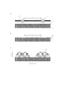
本発明に係る吐出口部材の製造工程について図5を参照して説明する。 The manufacturing process of the discharge port member according to the present invention will be described with reference to FIG.
まず、図5(a)に示すように、導電性の基体(導電性基板とも称す)1408を用意する。そして、図5(b)に示すように、導電性基板の上であって吐出口の形成位置に、吐出口の先端部分を形成する型材となる第1のマスク層1409’と該第1のマスク層の上に第2のマスク層1410’とからなる構造を形成する。つまり、導電性基板の上であって吐出口を形成する位置に、第1のマスク層1409’と第2のマスク層1410’とからなる構造を形成する。
First, as shown in FIG. 5A, a conductive substrate (also referred to as a conductive substrate) 1408 is prepared. Then, as shown in FIG. 5B, the
第1のマスク層1409’の厚さは、例えば、0.01〜10μmとすることができ、0.01〜3μmとすることが好ましく、0.1〜2μmとすることがより好ましい。
The thickness of the
第2のマスク層1410’の厚さは、例えば、1〜1000μmとすることができ、5〜200μmとすることが好ましく、10〜100μmとすることがより好ましい。
The thickness of the
導電性基板の材料としては、導電性を有するものであればよく、例えば、金属基板、また、樹脂、セラミック、ガラス等の材料上に導電層を形成したもの等を用いることができる。導電層は、銅、ニッケル、クロム、鉄等の導電性金属を素材にして、スパッタリング法、蒸着法、メッキ、イオンプレーティング法等の薄膜形成法によって形成する。 As a material of the conductive substrate, any material having conductivity can be used. For example, a metal substrate or a material in which a conductive layer is formed on a material such as resin, ceramic, glass, or the like can be used. The conductive layer is formed from a conductive metal such as copper, nickel, chromium, or iron by a thin film forming method such as a sputtering method, a vapor deposition method, plating, or an ion plating method.
次に、図5(c)に示すように、導電性基板の露出面に、電鋳法を用いて、高さが第1のマスク層の上面より上であって第2のマスク層の上面より下になるように第1のメッキ層1413を形成する。つまり、第1のメッキ処理を行うことにより、導電性基板1408の露出面上に第1のメッキ層1413を形成する。この際、第1のメッキ層の高さが第1のマスク層の上面より上であって第2のマスク層の上面より下になるように形成する。
Next, as shown in FIG. 5C, the upper surface of the second mask layer is formed on the exposed surface of the conductive substrate by using an electroforming method so that the height is higher than the upper surface of the first mask layer. A
第1のメッキ層1413の高さとしては、例えば2〜500μmとすることができ、5〜80μmとすることが好ましい。第1のメッキ層をこの範囲とすることで、より液滴の直進性を向上することができる。
The height of the
メッキ処理は、電鋳法を用いて行う。電鋳法としては、例えばスルファミン酸ニッケル浴等のメッキ浴に前記導電性基板を浸漬させて通電することで、ニッケル等を電析させる方法等をあげることができる。 The plating process is performed using an electroforming method. Examples of the electroforming method include a method in which nickel or the like is electrodeposited by immersing the conductive substrate in a plating bath such as a nickel sulfamate bath and energizing it.
次に、図5(d)に示すように、第2のマスク層を除去する。 Next, as shown in FIG. 5D, the second mask layer is removed.
次に、図5(e)に示すように、第1のメッキ層1413の周りに電鋳法を用いて第2のメッキ層1413’を形成し、吐出口を形成する。つまり、第2のメッキ処理を行い、第2のメッキ層1413’を形成し、吐出口を形成し、吐出口部材を形成する。
Next, as shown in FIG. 5E, a
第2のメッキ層の材料は、上述の第1のメッキ層の材料と異なるものを使用可能であるが、第2のメッキ層と第1のメッキ層との密着の観点から、第2のメッキ層と第1のメッキ層とが同じ材料であることが好ましい。 Although the material of the second plating layer can be different from the material of the first plating layer described above, the second plating layer is used from the viewpoint of adhesion between the second plating layer and the first plating layer. The layer and the first plating layer are preferably made of the same material.
図5(f)に示すように、本発明により形成される吐出口部材は、エッジを有さず、吐出口断面形状が直線部分を有するため、液滴の直進性を向上することができる。また、非常に高密度なノズル密度であっても、必要な吐出口部材の厚さを確保できる。したがって、本発明により、電鋳法を用いて、良好な吐出性能を有する吐出口部材を製造することができる。また、本発明は、電鋳法を用いて、高密度の吐出口を有する吐出口部材を製造することができる。 As shown in FIG. 5F, the discharge port member formed according to the present invention does not have an edge, and the discharge port cross-sectional shape has a straight line portion, so that the straightness of the droplet can be improved. Moreover, even if the nozzle density is very high, the necessary thickness of the discharge port member can be ensured. Therefore, according to the present invention, a discharge port member having good discharge performance can be manufactured using an electroforming method. Moreover, this invention can manufacture the discharge port member which has a high density discharge port using an electroforming method.
以下、図面を参照にして、本発明の実施形態について説明する。また、以下の説明では、本発明の適用例として、インクジェット記録ヘッドを例に挙げて説明するが、本発明の適用範囲はこれに限定されるものではなく、バイオッチップ作製や電子回路印刷用途の液体吐出ヘッドの製造にも適用できる。液体吐出ヘッドとしては、インクジェット記録ヘッドの他にも、例えばカラーフィルター製造用ヘッド等も挙げられる。 Hereinafter, embodiments of the present invention will be described with reference to the drawings. In the following description, an inkjet recording head will be described as an example of application of the present invention. However, the scope of application of the present invention is not limited to this, and liquid for biochip manufacturing and electronic circuit printing is used. It can also be applied to the manufacture of a discharge head. As the liquid discharge head, in addition to the ink jet recording head, for example, a head for producing a color filter can be cited.
(実施形態1)
以下、本発明の実施形態1について図を用いて説明する。
(Embodiment 1)
Hereinafter,
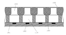
図1は、本実施形態で製造される液体吐出ヘッド用の吐出口部材の周辺を示した概略図である。また、図2は、図1のA−A’線における概略断面図である。 FIG. 1 is a schematic view showing the periphery of a discharge port member for a liquid discharge head manufactured in the present embodiment. FIG. 2 is a schematic sectional view taken along line A-A ′ of FIG. 1.
図2において、液体吐出ヘッド100は、素子基板101と、吐出口104に連通する流路115を構成する流路壁103と、を有する。また、素子基板101は、インクを吐出するためのエネルギーを発生させる複数のエネルギー発生素子(例えば発熱素子)102を含む。また、エネルギー発生素子102は流路115の下方に位置する。また、流路壁103は、素子基板101上にフォトリソ工程によって形成されている。また、吐出口部材105には、インクを吐出する吐出口104が形成されており、流路壁103の上に貼り合わされている。
In FIG. 2, the liquid discharge head 100 includes an
図1において、素子基板101は電極部(不図示)を有し、電気配線テープ106と電気的に接続されている。また、素子基板101と電気配線テープ106との電気的接続部分には、インクから電気接続部分を保護するリード封止剤107が塗布される。
In FIG. 1, the
素子基板101の材料としては、特に制限されるものではないが、例えばSiを挙げることができる。また、素子基板の厚さは、例えば0.2〜1mmとすることができる。
The material of the
流路壁103の材料としては、例えば感光性樹脂を用いることができ、光によるパターニングが可能な材料である。また、流路壁の材料は、インク等の液体に含まれる溶剤に耐えうる材料としてエポキシ樹脂が好ましい。
As the material of the
また、流路壁103と吐出口部材105との結合には接着剤を用いることができる。また、接着剤を用いずに、流路壁103を光パターニングした後、流路壁103と吐出口部材105とを貼り合わせて、加熱により接合することもできる。
Further, an adhesive can be used for coupling the
リード封止剤107の材料としては、熱或いは光によって硬化するエポキシ樹脂、アクリル樹脂であることが好ましいが、これらに限定されるものではなく、適宜選択することができる。
The material of the
本実施形態においては、例えば、ノズル間のピッチを1200dpi、吐出口の穴径d’を10μmとすることができる。 In the present embodiment, for example, the pitch between the nozzles can be set to 1200 dpi, and the hole diameter d ′ of the discharge ports can be set to 10 μm.
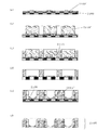
図3に、吐出口部材105を作製するための工程図を示す。
FIG. 3 is a process diagram for producing the
まず、図3(a)に示すように、導電性基板108の上に第1のマスク材料109及び第2のマスク材料110を積層する。なお、以下では、第1のマスク材料を下層レジスト材料、第2のマスクを上層レジスト材料とも称す。
First, as shown in FIG. 3A, a
第1及び第2のマスク材料としては、ネガ型、或いはポジ型のレジスト材料を用いることが可能であるが、除去の容易性を考えた場合、ポジ型レジストが望ましい。ポジ型レジストとしては、例えば、溶剤現像型のレジストであり、感応波長域250nm付近にピークを有するポリメチルメタクリレート(PMMA)等のメタクリル酸エステル樹脂、感応波長域290nm付近にピークを有するポリメチルイソプロペニルケトン樹脂、またアルカリ現像型のレジストであるジアゾナフトキノン樹脂などを用いることができる。
後述する第2のマスク材料の除去工程の際、第1のマスク材料を残しながら除去を行うため、第2のマスク材料は、第1のマスク材料と異なるレジスト材料を用いることが望ましい。
As the first and second mask materials, negative or positive resist materials can be used. However, in view of ease of removal, positive resists are desirable. As the positive resist, for example, a solvent development type resist, a methacrylic acid ester resin such as polymethyl methacrylate (PMMA) having a peak in the sensitive wavelength range of about 250 nm, or a polymethyl isopropyl having a peak in the sensitive wavelength range of about 290 nm. A propenyl ketone resin, a diazonaphthoquinone resin which is an alkali developing resist, or the like can be used.
In the step of removing the second mask material, which will be described later, in order to perform removal while leaving the first mask material, it is desirable to use a resist material different from the first mask material for the second mask material.
第2のマスク材料と第1のマスク材料の組み合わせは、例えば、ジアゾナフトキノン樹脂とPMMA樹脂、PMMA樹脂とポリメチルイソプロペニルケトン樹脂、ポリメチルイソプロペニルケトン樹脂とPMMA樹脂等を挙げることができる。第1のマスク材料としてジアゾナフトキノン樹脂を使用した場合、第2のマスク材料の現像液である溶剤現像液がジアゾナフトキノン樹脂を溶解させるため、ジアゾナフトキノン樹脂は第2のマスク材料としてのみ使用する。 Examples of the combination of the second mask material and the first mask material include diazonaphthoquinone resin and PMMA resin, PMMA resin and polymethyl isopropenyl ketone resin, polymethyl isopropenyl ketone resin and PMMA resin, and the like. When the diazonaphthoquinone resin is used as the first mask material, the solvent developer, which is the developer of the second mask material, dissolves the diazonaphthoquinone resin, so that the diazonaphthoquinone resin is used only as the second mask material.
本実施形態においては、例えば、下層レジスト材料109の厚みを1μm、上層レジスト材料110の厚みを12μmとすることができる。
In the present embodiment, for example, the thickness of the lower resist
次に、図3(b)に示すように、フォトマスク111を用いて、下層レジスト材料及び上層レジスト材料の所定位置に一括して露光光112を照射する。
Next, as shown in FIG. 3B,
次に、図3(c)に示すように、下層レジスト材料及び上層レジスト材料における露光光112が照射された領域を除去溶液により現像し、第1のマスク層109’及び第2のマスク層110’の積層構造を形成する。つまり、少なくとも吐出口の形成位置に相当する部分を残すように下層レジスト材料及び上層レジスト材料をパターニングし、第1のマスク層と第2のマスク層とからなる積層構造を形成する。つまり、第1のマスク層の側端面と第2のマスク層の側端面とが連続するように積層されている。なお、他の実施形態として、第1のマスク層の内側に第2のマスク層が配置されてもよく、第1のマスク層の側端面と上面とを覆うように第2のマスク層が配置されてもよい。
Next, as shown in FIG. 3C, the regions exposed to the
以下、第1のマスク層を下層レジスト、第2のマスク層を上層レジストとも称す。 Hereinafter, the first mask layer is also referred to as a lower layer resist, and the second mask layer is also referred to as an upper layer resist.
このとき、除去溶液としては、レジストが溶剤現像ポジ型レジストの場合、例えばメチルイソブチルケトン、シクロヘキサノン等を用い、レジストがアルカリ現像ポジ型レジストの場合、例えば、TMAH2〜10%溶液等を用いることができる。 At this time, as the removal solution, when the resist is a solvent development positive resist, for example, methyl isobutyl ketone, cyclohexanone, or the like is used. When the resist is an alkali development positive resist, for example, a TMAH 2 to 10% solution or the like is used. it can.
なお、第1のマスク層は、吐出口の先端部分を形成するための第1のマスク層となる。また、本実施形態で製造される吐出口部材では、吐出口の先端部分がメニスカス構造となる。 Note that the first mask layer is a first mask layer for forming the tip portion of the discharge port. Moreover, in the discharge port member manufactured by this embodiment, the front-end | tip part of a discharge port becomes a meniscus structure.
本実施形態においては、例えば、残った下層レジスト109’及び上層レジスト110’の幅D’(図3(c)参照)を14μmとすることができる。 In the present embodiment, for example, the width D ′ (see FIG. 3C) of the remaining lower layer resist 109 ′ and upper layer resist 110 ′ can be set to 14 μm.
次に、図3(d)に示すように、第1のメッキ処理を施し、下層レジスト材料及び上層レジスト材料を除去して露出した導電性基板上に第1のメッキ層113を形成する。この際、第1のメッキ層113の上面が、下層レジスト109’の上面より上で、且つ上層レジスト110’の上面より下に位置するように、第1のメッキ処理を行う。
Next, as shown in FIG. 3D, a first plating process is performed to remove the lower layer resist material and the upper layer resist material, thereby forming the first plated
メッキ材料、つまり吐出口部材の材料としては、例えばNiを用いることができる。また、Niの他にも、Pd、Cu若しくはAu又はそれらの複合材料等を用いることができる。また、その他にも、例えば、Ti、Zr、Hf、V、Cr、Mo、W、Mn、Tc、Re、Fe、Co、Ni、Ru、Os、Rh、Ir、Pt、Ag、Au、Ge、SiO2、Si3N4、Al2O3、BeO等の材料も選択してもよい。また、それぞれの金属中にテフロン(登録商標)等の樹脂成分を共析させてもよい。 As the plating material, that is, the material of the discharge port member, for example, Ni can be used. In addition to Ni, Pd, Cu, Au, or a composite material thereof can be used. In addition, for example, Ti, Zr, Hf, V, Cr, Mo, W, Mn, Tc, Re, Fe, Co, Ni, Ru, Os, Rh, Ir, Pt, Ag, Au, Ge, Materials such as SiO 2 , Si 3 N 4 , Al 2 O 3 , and BeO may also be selected. Further, a resin component such as Teflon (registered trademark) may be co-deposited in each metal.
メッキ処理としては、例えば電解メッキ、或いは無電解メッキ等により行うことができる。例えば、ガラス基板上にスパッタリング法によりPdやNiの薄膜を形成し、導電性基板を作製する。その後、第1のマスク層となるSiO2をスパッタリング法で形成する。その導電性基板をワークとして用い、導電性基板を陰極としてスルファミン酸ニッケル浴を用いて電気メッキを行い、導電性基板の上にNi電気メッキ物を成長させる。この際、浴中pHは3〜5、浴温度は、40〜60℃、陰極電流密度は、2〜50A/dm2である。 As the plating treatment, for example, electrolytic plating or electroless plating can be performed. For example, a thin film of Pd or Ni is formed on a glass substrate by sputtering to produce a conductive substrate. Thereafter, SiO 2 serving as a first mask layer is formed by a sputtering method. Using the conductive substrate as a work, electroplating is performed using a nickel sulfamate bath with the conductive substrate as a cathode, and a Ni electroplated material is grown on the conductive substrate. At this time, the pH in the bath is 3 to 5, the bath temperature is 40 to 60 ° C., and the cathode current density is 2 to 50 A / dm 2 .
本実施形態においては、例えば、第1のメッキ層の厚さtを10μmとすることができる。 In the present embodiment, for example, the thickness t of the first plating layer can be 10 μm.
次に、図3(e)に示すように、上層レジスト110’を除去する。 Next, as shown in FIG. 3E, the upper resist 110 'is removed.
この際、上層レジスト110’を除去する方法としては、第1のマスク層を溶解せず、第2のマスク層を溶解する溶解溶液を用いることにより行うことができる。上層レジストと下層レジストでは、感光波長の違いを用いる方法、或いは、異なる現像液で現像を行う方法、具体的には、アルカリ現像材料と溶剤現像材料を用いる方法がある。 At this time, a method of removing the upper resist 110 'can be performed by using a solution that dissolves the second mask layer without dissolving the first mask layer. For the upper layer resist and the lower layer resist, there are a method of using a difference in photosensitive wavelength, a method of developing with different developing solutions, specifically, a method of using an alkali developing material and a solvent developing material.
次に、図3(f)に示すように、第2のメッキ処理を行い、第1のメッキ層113の周りに第2のメッキ層113’を形成し、吐出口部材105を形成する。
Next, as shown in FIG. 3F, a second plating process is performed to form a
第2のメッキ処理は、例えば、この第1のメッキ層を陰極としてNi電気メッキ浴を用いて電気メッキを行い、第1のメッキ層にさらに等方的にメッキを成長させ、吐出口部材を形成することができる。 In the second plating process, for example, electroplating is performed using a Ni electroplating bath with the first plating layer as a cathode, and the plating is further grown isotropically on the first plating layer. Can be formed.
本実施形態においては、例えば、第1のメッキ層に等方的に2μmの厚みだけメッキを成長させることで、吐出口径d’を10μmとすることができる。また、本実施形態において、吐出口部材の厚みTは12μmとすることができる。 In the present embodiment, for example, the discharge port diameter d ′ can be set to 10 μm by growing the plating on the first plating layer isotropically to a thickness of 2 μm. In the present embodiment, the thickness T of the discharge port member can be 12 μm.
次に、図3(g)に示すように、下層レジスト109’を除去し、導電性基板108から吐出口部材105を外す。
Next, as shown in FIG. 3G, the lower layer resist 109 ′ is removed and the
なお、吐出口部材の吐出口径d’は、次式で表すことができる。 The discharge port diameter d ′ of the discharge port member can be expressed by the following equation.
d’≒D’−2(T−t) ・・・・・・(式2)
本発明の方法により製造される吐出口部材105は、図3(g)に示すように、湾曲部114にエッジを有しない形状である。また、非常に高密度なノズル密度であっても、必要な吐出口部材の厚さを確保できる。したがって、この吐出口部材105を流路壁103に貼り合わせて得られる液体吐出ヘッドは、吐出されたインク滴は非常に直進力を有するドットとなり、非常に良好な吐出性能を有する。
d′ ≈D′−2 (T−t) (Equation 2)
As shown in FIG. 3G, the
(実施形態2)
また、図6、図7に、吐出口が千鳥状に配列された場合の吐出口部材を有する液体吐出ヘッドの概略図を示す。例えば、本実施形態においてノズル間ピッチを1200dpiとする。
(Embodiment 2)
6 and 7 are schematic views of a liquid discharge head having discharge port members when the discharge ports are arranged in a staggered manner. For example, in this embodiment, the nozzle pitch is 1200 dpi.
この際、吐出口は千鳥状に配列しているため、吐出口間ピッチは600dpiとなるが、隣接する吐出口間には、千鳥配列における異なる列のインク流路(液流路)が存在する。流路壁303と吐出口部材305が接着される吐出口部材側は平らに形成されているため、流路壁303の接着信頼性は非常に高く、クロストーク等の心配もない。
At this time, since the ejection ports are arranged in a staggered pattern, the pitch between the ejection ports is 600 dpi, but between adjacent ejection ports, there are different rows of ink flow paths (liquid flow paths) in the staggered arrangement. . Since the discharge port member side to which the
(実施形態3)
図8に、実施形態1における下層レジストに無機材料を用いて、吐出口部材を製造する工程を示す。本実施形態では、実施形態1における第1のマスク層として絶縁材料であるSiO2膜を用いた形態について説明する。
(Embodiment 3)
FIG. 8 shows a process of manufacturing a discharge port member using an inorganic material for the lower layer resist in the first embodiment. In the present embodiment, a mode in which a SiO 2 film that is an insulating material is used as the first mask layer in the first embodiment will be described.
まず、図8(a)に示すように、導電性基板408上に固定部材として絶縁性を有するSiO2膜409を成膜する。そして、SiO2膜409の上にパターニング用レジスト411を成膜し、パターニングする。その後、SiO2膜409をエッチングガス412によってエッチングし、パターニングする。図8(b)は、パターニングされたSiO2膜409’を示す。
First, as shown in FIG. 8A, an insulating SiO 2 film 409 is formed on a
固定部材の材料としては、絶縁材料であり、導電性基板の上に固定して形成できるものであればよく、SiO2以外にも、例えば、SiN、SiC等の無機材料や、ポリイミド樹脂、エポキシ樹脂等の樹脂材料等を挙げることができる。 The material of the fixing member may be an insulating material that can be fixed on the conductive substrate. In addition to SiO 2 , for example, inorganic materials such as SiN and SiC, polyimide resin, epoxy Examples thereof include a resin material such as a resin.
次に、図8(c)に示すように、SiO2膜409’上に第2のマスク層410’を形成する。この際、本実施形態では、第2のマスク層410’の幅は、SiO2膜409’の幅と同じになるようにしている。つまり、第1のマスク層となるSiO2膜409’及び第2のマスク層は、側端面が連続するように積層する構造をとっている。
Next, as shown in FIG. 8C, a
次に、図8(d)に示すように、第1のメッキ処理を施し、導電性基板上に第1のメッキ層413を形成する。この際、第1のメッキ層413の上面が、SiO2膜409’の上面より上で、且つ第2のマスク層410’の上面より下に位置するように、第1のメッキ処理を行う。例えば、第2のマスク層及び第1のマスク層となるSiO2膜409’が存在しない領域でNiメッキが成長し、SiO2層409’の上面より上で、且つ第2のマスク層410’の上面より下の領域でめっき処理を止める。
Next, as shown in FIG. 8D, a first plating process is performed to form a
次に、図8(e)に示すように、第2のマスク層410’のみを除去する。 Next, as shown in FIG. 8E, only the second mask layer 410 'is removed.
次に、図8(f)に示すように、第2のメッキ処理を行い、第1のメッキ層413の周りに第2のメッキ層413’を形成し、吐出口部材405を形成する。
Next, as shown in FIG. 8 (f), a second plating process is performed to form a
図8(g)は、吐出口部材405を導電性基板408及びSiO2膜(固定部材)409’から取り外した状態を示す。
FIG. 8G shows a state where the
導電性部材と固定部材は強く接合しており、本発明の製造方法に再利用することができる。再度この基板を用いて吐出口部材を作製する際には、図8(c)の工程から始めることが可能となり、工程の簡略化及びコストダウンが図れる。 The conductive member and the fixing member are strongly joined and can be reused in the manufacturing method of the present invention. When the discharge port member is manufactured again using this substrate, it is possible to start from the process of FIG. 8C, and the process can be simplified and the cost can be reduced.
(実施形態4)
以下、本発明の実施形態を説明する。
(Embodiment 4)
Embodiments of the present invention will be described below.
図9(a)は、導電性基板2108上に下層レジスト2109’をパターニング形成した状態を示す。 FIG. 9A shows a state in which a lower layer resist 2109 ′ is formed by patterning on the conductive substrate 2108.
次に、図9(b)に示すように、下層レジスト2109’の上に上層レジスト材料を塗布してパターニングし、上層レジスト2110’を形成する。この際、上層レジストが下層レジストの上面と側端面を覆うように上層レジスト材料をパターニングする。 Next, as shown in FIG. 9B, an upper resist material is applied on the lower resist 2109 'and patterned to form an upper resist 2110'. At this time, the upper layer resist material is patterned so that the upper layer resist covers the upper surface and side end surfaces of the lower layer resist.
次に、図9(c)に示すように、導電性基板2108の上に第1のメッキ層2113を形成する。例えば、導電性基板2108の上であってレジストの存在しない領域にNiメッキを形成する。
Next, as illustrated in FIG. 9C, a
次に、図9(d)に示すように、上層レジスト2110’を除去する。 Next, as shown in FIG. 9D, the upper layer resist 2110 'is removed.
次に、図9(e)に示すように、第2のメッキ処理を行い、第1のメッキ層2113の周りに第2のメッキ層2113’を形成し、吐出口部材2105を形成する。この際、下層レジスト2109’上には、突起部2106が形成される。
Next, as shown in FIG. 9E, a second plating process is performed to form a
次に、図9(f)は、下層レジスト2109’を除去し、導電性基板2108から吐出口部材2105を取り外す。
Next, in FIG. 9F, the lower layer resist 2109 ′ is removed, and the
図10は、吐出口部材2105を流路壁2103に接合した状態を示す。流路壁2103は素子基板2101と接合している。吐出口部材2105には突起部2106があるため、吐出口2104付近では、突起部2106が無く、同一の吐出口面積の吐出口を有する吐出口部材の場合よりも、吐出口2104近傍にインクが多く存在する。そのため、吐出口2104の表面から蒸発した液体成分を、下に存在するインクからより多く補充可能である。従って、インクを吐出しない間に起こる吐出口の乾燥が低減される。したがって、吐出口部材2105を用いることで、吐出効率の向上が見込まれる。
FIG. 10 shows a state where the
以上の実施形態で示されるように、第1のマスク層を用いることで、吐出口にいわゆるメニスカス構造をもたせることができる。 As shown in the above embodiment, by using the first mask layer, the discharge port can have a so-called meniscus structure.
第1のマスク層と第2のマスク層とからなる構造は、図8(c)に示すように、面が一致して重なり合う積層構造とすることもできる。また、図9(b)に示すように、面方向において第1のマスク層の形状よりも第2のマスク層の形状の方が大きく、第2のマスク層が第1のマスク層を覆うような構造とすることもできる。また、それ以外にも、面方向において第2のマスク層の形状よりも第1のマスク層の形状の方が大きく、第2のマスク層は吐出先端型材の内側に形成されている積層構造とすることもできる。第1のマスク層と第2のマスク層とからなる構造をどのようなものとするかは、目的とする吐出口の形状を考慮して適宜選択することができる。 The structure composed of the first mask layer and the second mask layer may be a stacked structure in which the surfaces coincide and overlap as shown in FIG. Further, as shown in FIG. 9B, the shape of the second mask layer is larger than the shape of the first mask layer in the plane direction so that the second mask layer covers the first mask layer. It can also be made into a simple structure. In addition, the shape of the first mask layer is larger than the shape of the second mask layer in the plane direction, and the second mask layer is formed on the inner side of the discharge tip mold material. You can also The structure of the first mask layer and the second mask layer can be appropriately selected in consideration of the target discharge port shape.
Claims (10)
(1)前記吐出口を形成するための絶縁性の第1のマスクと、絶縁性の第2のマスクと、がこの順に積層された導電性の基体を用意する工程と、
(2)前記第1のマスクと前記第2のマスクとを利用してメッキを行い第1のメッキ層の上面の前記基体からの高さが、第1のマスクの上面の前記基体からの高さより高く、第2のマスクの上面の前記基体からの高さより低くなるように、前記第1のメッキ層を形成する工程と、
(3)前記第2のマスクを除去する工程と、
(4)前記第1のマスクをマスクとして利用して前記基体にメッキを行うことにより、第2のメッキ層を第1のメッキ層を覆うように形成する工程と、
(5)前記基体と前記第1のマスクとを除去することにより前記吐出口部材を形成する工程と、
をこの順に有する液体吐出ヘッドの製造方法。 A liquid passage that is provided with a substrate including an energy generating element that generates energy used for discharging a liquid, and a discharge port that discharges the liquid, and communicates with the discharge port by being joined to the substrate. A discharge port member for forming a liquid discharge head comprising:
(1) preparing a conductive substrate in which an insulating first mask for forming the discharge port and an insulating second mask are laminated in this order;
(2) Plating is performed using the first mask and the second mask, and the height of the upper surface of the first plating layer from the substrate is the height of the upper surface of the first mask from the substrate. Forming the first plating layer so as to be higher than the height of the upper surface of the second mask from the base, and
(3) removing the second mask;
(4) forming a second plating layer so as to cover the first plating layer by plating the base using the first mask as a mask;
(5) forming the discharge port member by removing the base and the first mask;
A method of manufacturing a liquid discharge head having the above in this order.
(1)前記吐出口を形成するための絶縁性の第1のマスクと、絶縁性の第2のマスクと、がこの順に積層された導電性の基体を用意する工程と、
(2)前記第1のマスクと前記第2のマスクとを利用してメッキを行い、第1のメッキ層の上面の前記基体からの高さが、第1のマスクの上面の前記基体からの高さより高く、第2のマスクの上面の前記基体からの高さより低くなるように、前記第1のメッキ層を形成する工程と、
(3)前記第2のマスクを除去する工程と、
(4)前記第1のマスクをマスクとして利用して前記基体にメッキを行うことにより、第2のメッキ層を第1のメッキ層を覆うように形成する工程と、
(5)前記基体と前記第1のマスクとを除去することにより前記吐出口部材を形成する工程と、
をこの順で有する吐出口部材の製造方法。 Used in the liquid discharge head for discharging the liquid, a process for the preparation of the discharge port member discharge opening is provided,
(1) preparing a conductive substrate in which an insulating first mask for forming the discharge port and an insulating second mask are laminated in this order;
(2) Plating is performed using the first mask and the second mask, and the height of the upper surface of the first plating layer from the base is from the base of the upper surface of the first mask. Forming the first plating layer so as to be higher than the height and lower than the height of the upper surface of the second mask from the substrate;
(3) removing the second mask;
(4) forming a second plating layer so as to cover the first plating layer by plating the base using the first mask as a mask;
(5) forming the discharge port member by removing the base and the first mask;
In this order.
Priority Applications (1)
| Application Number | Priority Date | Filing Date | Title |
|---|---|---|---|
| JP2010263680A JP5541732B2 (en) | 2009-11-26 | 2010-11-26 | Method for manufacturing liquid discharge head and method for manufacturing discharge port member |
Applications Claiming Priority (3)
| Application Number | Priority Date | Filing Date | Title |
|---|---|---|---|
| JP2009268758 | 2009-11-26 | ||
| JP2009268758 | 2009-11-26 | ||
| JP2010263680A JP5541732B2 (en) | 2009-11-26 | 2010-11-26 | Method for manufacturing liquid discharge head and method for manufacturing discharge port member |
Publications (3)
| Publication Number | Publication Date |
|---|---|
| JP2011131590A JP2011131590A (en) | 2011-07-07 |
| JP2011131590A5 JP2011131590A5 (en) | 2013-12-26 |
| JP5541732B2 true JP5541732B2 (en) | 2014-07-09 |
Family
ID=44061220
Family Applications (1)
| Application Number | Title | Priority Date | Filing Date |
|---|---|---|---|
| JP2010263680A Expired - Fee Related JP5541732B2 (en) | 2009-11-26 | 2010-11-26 | Method for manufacturing liquid discharge head and method for manufacturing discharge port member |
Country Status (3)
| Country | Link |
|---|---|
| US (1) | US8499453B2 (en) |
| JP (1) | JP5541732B2 (en) |
| CN (1) | CN102139568B (en) |
Families Citing this family (3)
| Publication number | Priority date | Publication date | Assignee | Title |
|---|---|---|---|---|
| JP5901149B2 (en) | 2011-06-01 | 2016-04-06 | キヤノン株式会社 | Liquid discharge head and manufacturing method thereof |
| JP6116198B2 (en) | 2012-11-15 | 2017-04-19 | キヤノン株式会社 | Method for manufacturing liquid discharge head |
| JP6818436B2 (en) * | 2016-05-27 | 2021-01-20 | キヤノン株式会社 | Recording element substrate, liquid discharge head and liquid discharge device |
Family Cites Families (39)
| Publication number | Priority date | Publication date | Assignee | Title |
|---|---|---|---|---|
| JPS58124660A (en) * | 1982-01-19 | 1983-07-25 | Ricoh Co Ltd | Manufacture of multinozzle plate of liquid injector |
| US4675083A (en) * | 1986-04-02 | 1987-06-23 | Hewlett-Packard Company | Compound bore nozzle for ink jet printhead and method of manufacture |
| JPH0349960A (en) | 1989-07-18 | 1991-03-04 | Seiko Epson Corp | Manufacture of ink jet |
| US4972204A (en) * | 1989-08-21 | 1990-11-20 | Eastman Kodak Company | Laminate, electroformed ink jet orifice plate construction |
| JPH04338550A (en) * | 1991-05-15 | 1992-11-25 | Brother Ind Ltd | Manufacture of orifice plate |
| JPH08132625A (en) | 1994-11-09 | 1996-05-28 | Ricoh Co Ltd | Production of nozzle plate and matrix structure therefor |
| EP0737582B1 (en) * | 1995-04-14 | 2002-07-10 | Canon Kabushiki Kaisha | Method for producing liquid ejecting head and liquid ejecting head obtained by the same method |
| JPH1016236A (en) | 1996-06-28 | 1998-01-20 | Copal Co Ltd | Ink jet printer head and its manufacturing method |
| JP3257960B2 (en) * | 1996-12-17 | 2002-02-18 | 富士通株式会社 | Inkjet head |
| JP3495218B2 (en) | 1997-03-24 | 2004-02-09 | 株式会社リコー | Method of manufacturing nozzle forming member |
| US5847725A (en) * | 1997-07-28 | 1998-12-08 | Hewlett-Packard Company | Expansion relief for orifice plate of thermal ink jet print head |
| US6449831B1 (en) * | 1998-06-19 | 2002-09-17 | Lexmark International, Inc | Process for making a heater chip module |
| RU2151066C1 (en) * | 1998-11-03 | 2000-06-20 | Самсунг Электроникс Ко., Лтд. | Microinjector nozzle plate assembly and method for its manufacture |
| EP1020291A3 (en) * | 1999-01-18 | 2001-04-11 | Canon Kabushiki Kaisha | Liquid discharge head and producing method therefor |
| JP3826608B2 (en) * | 1999-03-17 | 2006-09-27 | 富士写真フイルム株式会社 | Formation of water-repellent film on the surface of the liquid ejection part |
| EP1065059B1 (en) * | 1999-07-02 | 2007-01-31 | Canon Kabushiki Kaisha | Method for producing liquid discharge head, liquid discharge head, head cartridge, liquid discharging recording apparatus, method for producing silicon plate and silicon plate |
| JP2001038915A (en) | 1999-08-02 | 2001-02-13 | Seiko Epson Corp | Production of nozzle plate |
| JP2002059551A (en) | 2000-08-16 | 2002-02-26 | Ricoh Co Ltd | Ink jet nozzle and method of making the same |
| JP2003025577A (en) * | 2001-07-11 | 2003-01-29 | Canon Inc | Liquid jet head |
| JP4532785B2 (en) * | 2001-07-11 | 2010-08-25 | キヤノン株式会社 | Structure manufacturing method and liquid discharge head manufacturing method |
| US20030143492A1 (en) * | 2002-01-31 | 2003-07-31 | Scitex Digital Printing, Inc. | Mandrel with controlled release layer for multi-layer electroformed ink jet orifice plates |
| JP4068892B2 (en) * | 2002-05-20 | 2008-03-26 | 富士フイルム株式会社 | Image forming material |
| US7086154B2 (en) * | 2002-06-26 | 2006-08-08 | Brother Kogyo Kabushiki Kaisha | Process of manufacturing nozzle plate for ink-jet print head |
| JP4298414B2 (en) * | 2002-07-10 | 2009-07-22 | キヤノン株式会社 | Method for manufacturing liquid discharge head |
| JP4280574B2 (en) * | 2002-07-10 | 2009-06-17 | キヤノン株式会社 | Method for manufacturing liquid discharge head |
| JP3862624B2 (en) * | 2002-07-10 | 2006-12-27 | キヤノン株式会社 | Liquid discharge head and method for manufacturing the head |
| US7022417B2 (en) * | 2002-12-02 | 2006-04-04 | Nitto Kogyo Co., Ltd. | Metal belt and coated belt |
| JP2004268359A (en) * | 2003-03-07 | 2004-09-30 | Hitachi Printing Solutions Ltd | Inkjet head and its manufacturing method |
| JP2004323642A (en) * | 2003-04-23 | 2004-11-18 | Riso Kagaku Corp | Cationically polymerizable composition and ink |
| WO2005007413A1 (en) * | 2003-07-22 | 2005-01-27 | Canon Kabushiki Kaisha | Ink jet head and its manufacture method |
| EP1675724B1 (en) * | 2003-07-22 | 2012-03-28 | Canon Kabushiki Kaisha | Ink jet head and its manufacture method |
| JP4776154B2 (en) * | 2003-09-03 | 2011-09-21 | キヤノン株式会社 | Piezoelectric element, ink jet recording head, and method of manufacturing piezoelectric element |
| JP4537246B2 (en) * | 2004-05-06 | 2010-09-01 | キヤノン株式会社 | Method for manufacturing substrate for ink jet recording head and method for manufacturing recording head using the substrate manufactured by the method |
| EP1768848B1 (en) | 2004-06-28 | 2010-07-21 | Canon Kabushiki Kaisha | Liquid discharge head manufacturing method, and liquid discharge head obtained using this method |
| JP4459037B2 (en) * | 2004-12-01 | 2010-04-28 | キヤノン株式会社 | Liquid discharge head |
| JP4614383B2 (en) * | 2004-12-09 | 2011-01-19 | キヤノン株式会社 | Inkjet recording head manufacturing method and inkjet recording head |
| JP4667028B2 (en) * | 2004-12-09 | 2011-04-06 | キヤノン株式会社 | Structure forming method and ink jet recording head manufacturing method |
| KR100653088B1 (en) * | 2005-12-06 | 2006-12-04 | 삼성전자주식회사 | Fabrication method for inkjet print head |
| JP5085272B2 (en) * | 2007-02-09 | 2012-11-28 | 株式会社リコー | Liquid ejection head and image forming apparatus |
-
2010
- 2010-10-28 US US12/914,564 patent/US8499453B2/en not_active Expired - Fee Related
- 2010-11-23 CN CN201010556525.5A patent/CN102139568B/en not_active Expired - Fee Related
- 2010-11-26 JP JP2010263680A patent/JP5541732B2/en not_active Expired - Fee Related
Also Published As
| Publication number | Publication date |
|---|---|
| US20110120627A1 (en) | 2011-05-26 |
| CN102139568A (en) | 2011-08-03 |
| CN102139568B (en) | 2013-07-10 |
| US8499453B2 (en) | 2013-08-06 |
| JP2011131590A (en) | 2011-07-07 |
Similar Documents
| Publication | Publication Date | Title |
|---|---|---|
| US8429820B2 (en) | Method of manufacturing liquid discharge head | |
| JP4455287B2 (en) | Method for manufacturing ink jet recording head | |
| KR101438267B1 (en) | Liquid ejection head and process for producing the same | |
| JP5541732B2 (en) | Method for manufacturing liquid discharge head and method for manufacturing discharge port member | |
| JP5541733B2 (en) | Method for manufacturing discharge port member and method for manufacturing liquid discharge head | |
| US7205097B2 (en) | Liquid ejection head and method of producing the same | |
| JP2000117981A (en) | Ink jet printer head actuator and manufacture thereof | |
| JP5679688B2 (en) | Liquid discharge head and manufacturing method thereof | |
| JP5701014B2 (en) | Method for manufacturing ejection element substrate | |
| JP4015274B2 (en) | Manufacturing method of nozzle plate for inkjet head | |
| KR100289606B1 (en) | A patterning mathod of chamber plate for inkjet printhead and actuator manufactured thereby | |
| JP2000318163A (en) | Ink jet head, its manufacture and nozzle forming member and its manufacture | |
| JP3672559B2 (en) | Ink jet recording head chip manufacturing method, ink jet recording head manufacturing method, and recording apparatus | |
| JPH1120159A (en) | Ink jet head component and its manufacture | |
| JP2002059551A (en) | Ink jet nozzle and method of making the same | |
| JP3780735B2 (en) | Inkjet printer head manufacturing method | |
| JP3862235B2 (en) | Ink jet recording head, method for manufacturing the same, and recording apparatus | |
| JP3568022B2 (en) | Method of manufacturing inkjet head | |
| JP2006175678A (en) | Manufacturing method for nozzle sheet, surface treatment method for nozzle sheet, nozzle sheet, manufacturing method for liquid ejection head, and liquid ejection head | |
| JPH11188880A (en) | Electroforming support substrate, its production, and production of ink jet head part | |
| JP3166830B2 (en) | Manufacturing method of electrostatic suction type multi-nozzle inkjet head | |
| JP2017109389A (en) | Liquid discharge head, method for manufacturing liquid discharge head and recovery method | |
| JPH054346A (en) | Manufacture of ink jet head | |
| JP2002059553A (en) | Method of making nozzle plate and nozzle plate | |
| JP2001073181A (en) | Electroforming original plate blank, electroforming original plate, production of electroforming parts and production of diaphragm |
Legal Events
| Date | Code | Title | Description |
|---|---|---|---|
| A521 | Request for written amendment filed |
Free format text: JAPANESE INTERMEDIATE CODE: A523 Effective date: 20131113 |
|
| A621 | Written request for application examination |
Free format text: JAPANESE INTERMEDIATE CODE: A621 Effective date: 20131113 |
|
| A977 | Report on retrieval |
Free format text: JAPANESE INTERMEDIATE CODE: A971007 Effective date: 20140311 |
|
| TRDD | Decision of grant or rejection written | ||
| A01 | Written decision to grant a patent or to grant a registration (utility model) |
Free format text: JAPANESE INTERMEDIATE CODE: A01 Effective date: 20140408 |
|
| A61 | First payment of annual fees (during grant procedure) |
Free format text: JAPANESE INTERMEDIATE CODE: A61 Effective date: 20140430 |
|
| R151 | Written notification of patent or utility model registration |
Ref document number: 5541732 Country of ref document: JP Free format text: JAPANESE INTERMEDIATE CODE: R151 |
|
| LAPS | Cancellation because of no payment of annual fees |