JP5539895B2 - Method for electrically connecting an electrically isolated printhead die ground network with a flexible circuit - Google Patents
Method for electrically connecting an electrically isolated printhead die ground network with a flexible circuit Download PDFInfo
- Publication number
- JP5539895B2 JP5539895B2 JP2010535944A JP2010535944A JP5539895B2 JP 5539895 B2 JP5539895 B2 JP 5539895B2 JP 2010535944 A JP2010535944 A JP 2010535944A JP 2010535944 A JP2010535944 A JP 2010535944A JP 5539895 B2 JP5539895 B2 JP 5539895B2
- Authority
- JP
- Japan
- Prior art keywords
- ground network
- layer
- metal layer
- printhead
- printhead die
- Prior art date
- Legal status (The legal status is an assumption and is not a legal conclusion. Google has not performed a legal analysis and makes no representation as to the accuracy of the status listed.)
- Active
Links
- 238000000034 method Methods 0.000 title claims description 8
- 239000000758 substrate Substances 0.000 claims abstract description 33
- 238000007641 inkjet printing Methods 0.000 claims abstract description 29
- 229910052751 metal Inorganic materials 0.000 claims description 44
- 239000002184 metal Substances 0.000 claims description 44
- 238000004519 manufacturing process Methods 0.000 claims description 12
- XUIMIQQOPSSXEZ-UHFFFAOYSA-N Silicon Chemical compound [Si] XUIMIQQOPSSXEZ-UHFFFAOYSA-N 0.000 claims description 10
- 229910052710 silicon Inorganic materials 0.000 claims description 10
- 239000010703 silicon Substances 0.000 claims description 10
- 238000010438 heat treatment Methods 0.000 claims description 9
- WGTYBPLFGIVFAS-UHFFFAOYSA-M tetramethylammonium hydroxide Chemical compound [OH-].C[N+](C)(C)C WGTYBPLFGIVFAS-UHFFFAOYSA-M 0.000 claims description 8
- 238000005530 etching Methods 0.000 claims description 6
- 229910000838 Al alloy Inorganic materials 0.000 claims description 3
- RVSGESPTHDDNTH-UHFFFAOYSA-N alumane;tantalum Chemical compound [AlH3].[Ta] RVSGESPTHDDNTH-UHFFFAOYSA-N 0.000 claims description 3
- 229910052782 aluminium Inorganic materials 0.000 claims description 3
- XAGFODPZIPBFFR-UHFFFAOYSA-N aluminium Chemical compound [Al] XAGFODPZIPBFFR-UHFFFAOYSA-N 0.000 claims description 3
- PCHJSUWPFVWCPO-UHFFFAOYSA-N gold Chemical compound [Au] PCHJSUWPFVWCPO-UHFFFAOYSA-N 0.000 claims description 3
- 239000010931 gold Substances 0.000 claims description 3
- 229910052737 gold Inorganic materials 0.000 claims description 3
- 239000010410 layer Substances 0.000 description 76
- 230000009286 beneficial effect Effects 0.000 description 2
- 238000010586 diagram Methods 0.000 description 2
- 239000005360 phosphosilicate glass Substances 0.000 description 2
- 229910021420 polycrystalline silicon Inorganic materials 0.000 description 2
- 239000011241 protective layer Substances 0.000 description 2
- 239000004065 semiconductor Substances 0.000 description 2
- 239000010409 thin film Substances 0.000 description 2
- 229910052581 Si3N4 Inorganic materials 0.000 description 1
- 239000004020 conductor Substances 0.000 description 1
- 229920005591 polysilicon Polymers 0.000 description 1
- HBMJWWWQQXIZIP-UHFFFAOYSA-N silicon carbide Chemical compound [Si+]#[C-] HBMJWWWQQXIZIP-UHFFFAOYSA-N 0.000 description 1
- 229910010271 silicon carbide Inorganic materials 0.000 description 1
- HQVNEWCFYHHQES-UHFFFAOYSA-N silicon nitride Chemical compound N12[Si]34N5[Si]62N3[Si]51N64 HQVNEWCFYHHQES-UHFFFAOYSA-N 0.000 description 1
- 229910052715 tantalum Inorganic materials 0.000 description 1
- GUVRBAGPIYLISA-UHFFFAOYSA-N tantalum atom Chemical compound [Ta] GUVRBAGPIYLISA-UHFFFAOYSA-N 0.000 description 1
Images


Classifications
-
- B—PERFORMING OPERATIONS; TRANSPORTING
- B41—PRINTING; LINING MACHINES; TYPEWRITERS; STAMPS
- B41J—TYPEWRITERS; SELECTIVE PRINTING MECHANISMS, i.e. MECHANISMS PRINTING OTHERWISE THAN FROM A FORME; CORRECTION OF TYPOGRAPHICAL ERRORS
- B41J2/00—Typewriters or selective printing mechanisms characterised by the printing or marking process for which they are designed
- B41J2/005—Typewriters or selective printing mechanisms characterised by the printing or marking process for which they are designed characterised by bringing liquid or particles selectively into contact with a printing material
- B41J2/01—Ink jet
- B41J2/135—Nozzles
- B41J2/14—Structure thereof only for on-demand ink jet heads
- B41J2/14016—Structure of bubble jet print heads
- B41J2/14088—Structure of heating means
- B41J2/14112—Resistive element
- B41J2/14129—Layer structure
-
- B—PERFORMING OPERATIONS; TRANSPORTING
- B41—PRINTING; LINING MACHINES; TYPEWRITERS; STAMPS
- B41J—TYPEWRITERS; SELECTIVE PRINTING MECHANISMS, i.e. MECHANISMS PRINTING OTHERWISE THAN FROM A FORME; CORRECTION OF TYPOGRAPHICAL ERRORS
- B41J2/00—Typewriters or selective printing mechanisms characterised by the printing or marking process for which they are designed
- B41J2/005—Typewriters or selective printing mechanisms characterised by the printing or marking process for which they are designed characterised by bringing liquid or particles selectively into contact with a printing material
- B41J2/01—Ink jet
- B41J2/135—Nozzles
- B41J2/14—Structure thereof only for on-demand ink jet heads
- B41J2/14016—Structure of bubble jet print heads
- B41J2/14072—Electrical connections, e.g. details on electrodes, connecting the chip to the outside...
-
- B—PERFORMING OPERATIONS; TRANSPORTING
- B41—PRINTING; LINING MACHINES; TYPEWRITERS; STAMPS
- B41J—TYPEWRITERS; SELECTIVE PRINTING MECHANISMS, i.e. MECHANISMS PRINTING OTHERWISE THAN FROM A FORME; CORRECTION OF TYPOGRAPHICAL ERRORS
- B41J2/00—Typewriters or selective printing mechanisms characterised by the printing or marking process for which they are designed
- B41J2/005—Typewriters or selective printing mechanisms characterised by the printing or marking process for which they are designed characterised by bringing liquid or particles selectively into contact with a printing material
- B41J2/01—Ink jet
- B41J2/135—Nozzles
- B41J2/14—Structure thereof only for on-demand ink jet heads
- B41J2/1433—Structure of nozzle plates
-
- B—PERFORMING OPERATIONS; TRANSPORTING
- B41—PRINTING; LINING MACHINES; TYPEWRITERS; STAMPS
- B41J—TYPEWRITERS; SELECTIVE PRINTING MECHANISMS, i.e. MECHANISMS PRINTING OTHERWISE THAN FROM A FORME; CORRECTION OF TYPOGRAPHICAL ERRORS
- B41J2/00—Typewriters or selective printing mechanisms characterised by the printing or marking process for which they are designed
- B41J2/005—Typewriters or selective printing mechanisms characterised by the printing or marking process for which they are designed characterised by bringing liquid or particles selectively into contact with a printing material
- B41J2/01—Ink jet
- B41J2/135—Nozzles
- B41J2/16—Production of nozzles
- B41J2/1601—Production of bubble jet print heads
-
- B—PERFORMING OPERATIONS; TRANSPORTING
- B41—PRINTING; LINING MACHINES; TYPEWRITERS; STAMPS
- B41J—TYPEWRITERS; SELECTIVE PRINTING MECHANISMS, i.e. MECHANISMS PRINTING OTHERWISE THAN FROM A FORME; CORRECTION OF TYPOGRAPHICAL ERRORS
- B41J2/00—Typewriters or selective printing mechanisms characterised by the printing or marking process for which they are designed
- B41J2/005—Typewriters or selective printing mechanisms characterised by the printing or marking process for which they are designed characterised by bringing liquid or particles selectively into contact with a printing material
- B41J2/01—Ink jet
- B41J2/135—Nozzles
- B41J2/16—Production of nozzles
- B41J2/1621—Manufacturing processes
- B41J2/1626—Manufacturing processes etching
- B41J2/1629—Manufacturing processes etching wet etching
-
- B—PERFORMING OPERATIONS; TRANSPORTING
- B41—PRINTING; LINING MACHINES; TYPEWRITERS; STAMPS
- B41J—TYPEWRITERS; SELECTIVE PRINTING MECHANISMS, i.e. MECHANISMS PRINTING OTHERWISE THAN FROM A FORME; CORRECTION OF TYPOGRAPHICAL ERRORS
- B41J2/00—Typewriters or selective printing mechanisms characterised by the printing or marking process for which they are designed
- B41J2/005—Typewriters or selective printing mechanisms characterised by the printing or marking process for which they are designed characterised by bringing liquid or particles selectively into contact with a printing material
- B41J2/01—Ink jet
- B41J2/135—Nozzles
- B41J2/14—Structure thereof only for on-demand ink jet heads
- B41J2002/14491—Electrical connection
Abstract
Description
インクジェット印刷装置は、プリントヘッドダイを介してインクを紙等の媒体上に噴射して媒体上に画像を形成する。プリントヘッドダイは比較的小さい半導体部品であり、プリントヘッドダイが通常有する多数の複雑な構成部材はダイを適切に動作させるために精密に製造する必要がある。プリントヘッドダイの多くはシリコン基板および基板上に形成される素子層を含む。素子層は、トランジスタ、発熱抵抗体、およびダイを適切に動作させるためのその他の部材を含んでいてもよい。 An ink jet printing apparatus forms an image on a medium by ejecting ink onto a medium such as paper via a print head die. A printhead die is a relatively small semiconductor component, and the many complex components that a printhead die normally has to be precisely manufactured in order for the die to operate properly. Many printhead dies include a silicon substrate and a device layer formed on the substrate. The element layer may include a transistor, a heating resistor, and other members for properly operating the die.
プリントヘッドダイの多くの種類において、シリコン基板と素子層はプリントヘッドダイの最適動作のために接地されている。しかしながら、プリントヘッドダイの製造過程において、シリコン基板と素子層の接地は問題を発生させる場合がある。詳細には、シリコン基板と素子層とが接地されている場合、シリコン基板のエッチングを含む製造工程が最適に実行されない場合がある。 In many types of printhead dies, the silicon substrate and device layers are grounded for optimal operation of the printhead die. However, in the manufacturing process of the printhead die, the grounding of the silicon substrate and the element layer may cause a problem. Specifically, when the silicon substrate and the element layer are grounded, a manufacturing process including etching of the silicon substrate may not be optimally performed.
図1は、本開示の実施の形態によるインクジェット印刷装置用プリントヘッドアセンブリ100の典型例を示す。プリントヘッドアセンブリ100は封入カートリッジ102を含む。封入カートリッジ102、すなわちプリントヘッドアセンブリ100はインクジェット印刷装置の対応するスロットに挿入可能であり、これにより装置は紙等の媒体上にインクを噴射して媒体上に画像を形成できる。
FIG. 1 shows a typical example of a
プリントヘッドアセンブリ100は、アセンブリ100のフレキシブル回路106に電気的に接続されるプリントヘッドダイ104を含む。プリントヘッドダイ104は通常小さい半導体ダイであり、図1においては、明確に図示するためにフレキシブル回路106および封入カートリッジ102に対する実際の大きさよりも大きい縮尺で図示する。フレキシブル回路106は、インクジェット印刷装置に着脱可能に挿入又は取付けられる封入カートリッジ102上で、インクジェット印刷装置の対応する電気コネクタと電気的に結合する。詳細には、フレキシブル回路106はプリントヘッドダイ104からの導線を含むことにより、ダイ104をインクジェット印刷装置に電気的に結合してもよい。回路106は柔軟性を有するため、図1に示すように、封入カートリッジ102の少なくとも1個の縁周りで屈曲可能である。
The
図1の実施の形態において、プリントヘッドアセンブリ100はまた封入カートリッジ102内部に含まれるインク108の供給を含む。しかしながら、他の実施の形態においては、インク108の供給はプリントヘッドアセンブリ100とは異なるアセンブリ内に含まれていてもよい。通常、プリントヘッドアセンブリ100が取付けられたインクジェット印刷装置は、プリントヘッドダイ104にインク108のドロップをダイを介して噴射させて紙等の媒体上に画像を形成する。
In the embodiment of FIG. 1, the
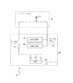
図2は、本開示の実施の形態によるインクジェット印刷装置用プリントヘッドアセンブリ100の部分概略図である。詳細には、プリントヘッドアセンブリ100のプリントヘッドダイ104およびフレキシブル回路106が図2に示される。図示のプリントヘッドダイ104は、例えばシリコン基板等の基板202を含む。基板202はプリントヘッドダイ104の基板であり、基板202上には例えばトランジスタおよび発熱抵抗体等、ダイ104の様々な装置が製造される。基板202は第1の接地ネットワーク206に電気的に接続される。すなわち、第1の接地ネットワーク206は基板202の複数部分に電気的に接続される。
FIG. 2 is a partial schematic diagram of a
図示のプリントヘッドダイ104はまた、装置接地部208および表面金属層210を含む。装置接地部208はプリントヘッドダイ104上に製造される装置の接地接続部であり、例えばプリントヘッドダイ104上に製造される様々なトランジスタの接地部である。表面金属層210は詳細には金からなる層であってもよい。一実施の形態における表面金属層210は、プリントヘッドダイ104内の電力信号および接地信号に低抵抗の導体を提供する。装置接地部208および表面金属層210は第2の接地ネットワーク212に電気的に接続される。
The illustrated
プリントヘッドダイ104の動作中において、第1の接地ネットワーク206に比べてより大量の電流が第2の接地ネットワーク212を流れるため、第2の接地ネットワーク212を主の接地ネットワーク、そして第1の接地ネットワーク206を副の、又は「裏の」接地ネットワークと考えてもよい。なお、プリントヘッドダイ104内部において、第1の接地ネットワーク206および第2の接地ネットワーク212は相互に電気的に絶縁される。このことは、プリントヘッドダイ104の製造中に用いられる例えばエッチング等の処理において、第2の接地ネットワーク212を第1の接地ネットワーク206とは異なる電位にすることができるため有益である。したがって、プリントヘッドダイ104内に相互に電気的に絶縁される接地ネットワーク206および212を有することは、ダイ104の製造中に有益である。
During operation of the
しかしながら、プリントヘッドダイ104の動作中において、第1の接地ネットワーク206および第2の接地ネットワーク212は同一の電位、詳細には、例えばアース等の共有電位又は接地電位に保持することが可能である。図2の実施の形態は、フレキシブル回路106において接地ネットワーク206および212を相互に電気的に接続する。詳細には、接地ネットワーク206および212はフレキシブル回路106内の少なくとも1個の点214において接する。点214は例えば、プリントヘッドダイ104をプリントヘッドアセンブリ100が挿入又は取付けられたインクジェット印刷装置に電気的に接続するインクジェット印刷装置用コネクタピンとして実装してもよい。
However, during operation of the
したがって、図2の実施の形態はプリントヘッドダイ104の製造中および動作中に、接地ネットワーク206および212に少なくとも略最適な電位を提供する。プリントヘッドダイ104の製造中は、接地ネットワーク206および212は電気的に絶縁されるため、異なる電位を有することが可能である。プリントヘッドダイ104の動作中は、接地ネットワーク206および212はフレキシブル回路106において相互に電気的に接続されるため、同一の接地電位又は共有電位に保持される。
Accordingly, the embodiment of FIG. 2 provides at least a substantially optimal potential for the
図3は、本発明の実施の形態によるプリントヘッドダイ104の部分断面図である。プリントヘッドダイ104上には素子層302が配置される。素子層302は複数の薄膜トランジスタを含む。例えば、あるトランジスタはソース304A、多結晶シリコンゲート304B、およびドレイン304Cを含み、ゲート304B、ソース304A、およびドレイン304C間にはゲート酸化物からなる小さい層(図3においては特に符号を付さない)が形成される。他のトランジスタはソース306A、多結晶シリコンゲート306B、およびドレイン306Cを含み、ゲート306B、ソース306A、およびドレイン306C間にはゲート酸化物からなる小さい層が形成される。ドレイン304Cはドレイン306Cと同一である。
FIG. 3 is a partial cross-sectional view of
素子層302はまた、図3においては発熱抵抗体316は図示の簡便性を考慮して分割して図示した素子層302上に配置されているが、発熱抵抗体316を含むとしてもよい。当業者であれば理解できる通り、電流が発熱抵抗体316に供給されると、抵抗体316は「燃焼させられる」と考えられる。したがって、抵抗体316は、プリントヘッドダイ104の最上部側に位置するインク内に気泡を形成させる。この気泡はダイ104からインクドロップを噴射する。その後、気泡は潰れる。更に、素子層302は絶縁層307を含むとすることもでき、一実施の形態において素子層302はリン珪酸ガラス(PSG)であってもよい。
In FIG. 3, the
素子層302上には薄い抵抗層308が配置され、その上には第1の金属層310が配置される。第1の金属層310は例えばアルミニウムおよび/又はタンタルアルミニウム合金からなっていてもよく、これにより層310は1個のアルミニウム層および1個のタンタルアルミニウム合金層からなる2個の副層を有する。第1の金属層310上には受動層および/又は絶縁層312が配置され、プリントヘッドダイ104をインクから保護する。層312は例えば炭化珪素又は窒化珪素からなっていてもよい。発熱抵抗体316は絶縁層307の一部、抵抗層308の一部、第1の金属層310の一部、層312の一部、および/又は受動層312上に配置される更なる保護層314の一部を含むとしてもよい。
A
素子層302上、詳細には第1の金属層310上には表面金属層210が配置され、表面金属層210はタンタル層も含む第2の金属層の副層であってもよい。表面金属層210は、層312の一部により第1の金属層310から分離および電気的に絶縁される。図3の断面図には電気的接続については記載していないが、表面金属層210は素子層302内のトランジスタの接地部に電気接続し、また例えば主電源接地部およびその他の接地部に電気的に接続していてもよい。しかしながら、図1および図2のフレキシブル回路106は表面金属層210を介して図2の第2の接地ネットワーク212に電気的に接続される。また、第2の接地ネットワーク212は表面金属層210を含む第2の金属層に実装されているとしてもよい。更に、第2の接地ネットワーク212は主としては第1の金属層310に実装されていないとしてもよい。
A
図3の分割線317は、プリントヘッドダイ104上において、線317の左側の部分が線317の右側の部分から図3に示す状態より遠くに配置されていることを示す。線317の左側の部分は、基板接点318を含む。接点318においては第1の金属層310の一部が露出し、受動層312、保護層314、および絶縁層307のいずれも配置されない。したがって、基板202上方の2個の層、すなわち薄い抵抗層308および第1の金属層310は両方とも導電性を有するため、接点318においては第1の金属層310は基板202を電気的に露出する。図1および図2のフレキシブル回路は、第1の金属層310を介して図2の第1の接地ネットワーク206に電気的に接続される。また、第1の接地ネットワーク206は主として第1の金属層310に実装されるとしてもよい。
The
したがって、図3は、プリントヘッドダイ104において図2の接地ネットワーク206および212が相互に電気的に絶縁される様子を示す。例えば表面金属層210は、第1の金属層310における接点318が配置される部分から電気的に絶縁される。したがって、第2の接地ネットワーク212が表面金属層210を含む第2の金属層に実装され、第1の接地ネットワーク206が主として第1の金属層310に実装された場合、接地ネットワーク206および212はプリントヘッドダイ104内で相互に電気的に絶縁される。
Thus, FIG. 3 illustrates how the
図4は、本開示の実施の形態による、インクジェット印刷装置用プリントヘッドアセンブリ100の少なくとも一部を製造する方法400を示す。なお、図4では製造工程の一部のみを詳細に示し、ここで説明する。したがって、当業者であれば、プリントヘッドアセンブリ100の製造を完了するために、その他の工程を実行してもよいと理解するものとする。詳細には、図4では本開示の実施の形態に関連する部分のみ示し、ここで説明する。
FIG. 4 illustrates a
プリントヘッドアセンブリ100のプリントヘッドダイ104に基板202を設ける(402)。その後、薄膜トランジスタおよび/又は発熱抵抗体316を含む素子層302を基板上に形成してもよい(404)。その後、任意の時点で第1の金属層310を素子層302上に形成(406)し、上述のように第1の接地ネットワーク206が主として第1の金属層310に実装される。最後に、表面金属層210を第1の金属層310上に形成(408)し、上述のように第2の接地ネットワーク212が表面金属層210を含む第2の金属層に実装される。
A
第1の接地ネットワーク206と第2の接地ネットワーク212とが異なる電位となるようにして、基板202をエッチングしてもよい(410)。例えば、基板202は水酸化テトラメチルアンモニウム(TMAH)を用いてウェットエッチングしてもよい。TMAHによる基板202のエッチングは、表面金属層210(すなわち、第2の接地ネットワーク212)が基板202(すなわち、第1の接地ネットワーク206)に対して任意の電位を有する場合に最適に実行されることが分かっている。そうでない場合、基板202は不適切にエッチングされる可能性がある。当業者であれば理解できる通り、基板202をエッチングしてプリントヘッドダイ104を介してインクを供給するための孔を形成してもよく、および/又は、発熱抵抗体316近傍に凹凸がなく平滑な縁を形成してもよい。本発明の実施の形態によれば、フレキシブル回路106がダイ104に接続される前に、基板202および表面金属層210(すなわち、第1の接地ネットワーク206および第2の接地ネットワーク212)がプリントヘッドダイ104内で相互に電気的に絶縁されている場合、表面金属層210は基板202に対して任意の電位を有することができる。
The
エッチングが完了すると、フレキシブル回路106をプリントヘッドダイ104に接続してもよく(412)、これにより第1の接地ネットワーク206および第2の接地ネットワーク212が相互に電気的に接続される。したがって、プリントヘッドアセンブリ100の使用中に、接地ネットワーク206および212(すなわち、表面金属層210および基板202又は第1の金属層310)は同一の接地電位又はその他の共有電位に保持され、その結果、アセンブリ100が最適に動作することが分かった。したがって、プリントヘッドアセンブリ100の使用中において、接地ネットワーク206および212はフレキシブル回路106において相互に電気的に接続されるため、相互に電気接続された状態に保持される。
When the etching is complete, the
最後に、図5は本開示の実施の形態による基本的なインクジェット印刷装置500を示す。インクジェット印刷装置500はインクジェットプリンタ、多機能機器(MFD)又はインクジェット印刷機能以外の機能性も備えることができるオールインワン(AIO)機器であってもよい。図5に示すインクジェット印刷装置500は、上述のプリントヘッドアセンブリ100およびインクジェット印刷機構502を含む。当業者であれば、インクジェット印刷装置500は図5に示す構成部材に加えてその他の部材を含んでいてもよく、通常はそのようなその他の部材を含むと理解するであろう。
Finally, FIG. 5 shows a basic
インクジェット印刷機構502は、インクジェット印刷装置500が例えばインクを媒体上に熱的に噴射することにより紙等の媒体上に画像を形成するための構成部材を含む。したがって、プリントヘッドアセンブリ100はインクジェット印刷機構502と構成部材を共有していてもよい。すなわち、プリントヘッドアセンブリ100は、実際にインクを噴射させるプリントヘッドダイ104を含む。この点において、インクジェット印刷機構502はプリントヘッドダイ104をプリントヘッドアセンブリ100と共有すると考えてもよい。当業者であれば理解できる通り、インクジェット印刷機構502はファームウェアおよび媒体送りモータ等、その他の構成部材を含んでいてもよい。
The
Claims (5)
該プリントヘッドアセンブリのプリントヘッドダイのためのシリコン基板を設け、
少なくとも1個のトランジスタ、および前記プリントヘッドアセンブリからインクを噴射させる発熱抵抗体を含む素子層を前記シリコン基板上に形成し、
前記シリコン基板に電気的に接続される第1の接地ネットワークを提供する第1の金属層を前記素子層上に形成し、
該第1の金属層上に絶縁層を形成し、
前記素子層に電気的に接続される第2の接地ネットワークを提供する第2の金属層を前記絶縁層上に形成して、前記プリントヘッドダイ内で前記第2の接地ネットワークを前記第1の接地ネットワークから電気的に絶縁し、
エッチングの最中に前記第1の接地ネットワークが前記第2の接地ネットワークとは異なる電位に保持されるように前記シリコン基板を水酸化テトラメチルアンモニウムエッチャントを用いてエッチングすることを含むことを特徴とする、インクジェット印刷装置のためのプリントヘッドアセンブリの作製方法。 A method of making a printhead assembly for an inkjet printing apparatus, comprising:
The silicon substrate for the printhead die 該Pu printhead assembly provided,
Forming an element layer on the silicon substrate including at least one transistor and a heating resistor for ejecting ink from the printhead assembly;
Forming a first metal layer on the device layer to provide a first ground network electrically connected to the silicon substrate;
Forming an insulating layer on the first metal layer;
A second metal layer is provided on the insulating layer to provide a second ground network that is electrically connected to the element layer, and the second ground network is formed in the printhead die. Electrically isolated from the ground network,
Etching the silicon substrate with a tetramethylammonium hydroxide etchant so that the first ground network is held at a different potential than the second ground network during etching. A method of making a printhead assembly for an inkjet printing apparatus .
Applications Claiming Priority (1)
| Application Number | Priority Date | Filing Date | Title |
|---|---|---|---|
| PCT/US2007/086210 WO2009073019A1 (en) | 2007-12-02 | 2007-12-02 | Electrically connecting electrically isolated printhead die ground networks as flexible circuit |
Related Child Applications (1)
| Application Number | Title | Priority Date | Filing Date |
|---|---|---|---|
| JP2014057481A Division JP5777762B2 (en) | 2014-03-20 | 2014-03-20 | Method for electrically connecting an electrically isolated printhead die ground network with a flexible circuit |
Publications (2)
| Publication Number | Publication Date |
|---|---|
| JP2011505272A JP2011505272A (en) | 2011-02-24 |
| JP5539895B2 true JP5539895B2 (en) | 2014-07-02 |
Family
ID=40718005
Family Applications (1)
| Application Number | Title | Priority Date | Filing Date |
|---|---|---|---|
| JP2010535944A Active JP5539895B2 (en) | 2007-12-02 | 2007-12-02 | Method for electrically connecting an electrically isolated printhead die ground network with a flexible circuit |
Country Status (10)
| Country | Link |
|---|---|
| US (2) | US9555630B2 (en) |
| EP (1) | EP2229279B1 (en) |
| JP (1) | JP5539895B2 (en) |
| CN (1) | CN101883683B (en) |
| AT (1) | ATE553928T1 (en) |
| ES (1) | ES2386481T3 (en) |
| PL (1) | PL2229279T3 (en) |
| PT (1) | PT2229279E (en) |
| TW (1) | TWI467657B (en) |
| WO (1) | WO2009073019A1 (en) |
Families Citing this family (4)
| Publication number | Priority date | Publication date | Assignee | Title |
|---|---|---|---|---|
| US9257763B2 (en) | 2013-07-02 | 2016-02-09 | Gyrus Acmi, Inc. | Hybrid interconnect |
| US9510739B2 (en) | 2013-07-12 | 2016-12-06 | Gyrus Acmi, Inc. | Endoscope small imaging system |
| JP6730432B2 (en) * | 2016-02-24 | 2020-07-29 | ヒューレット−パッカード デベロップメント カンパニー エル.ピー.Hewlett‐Packard Development Company, L.P. | Fluid ejection device including integrated circuit |
| JP6976743B2 (en) * | 2017-06-29 | 2021-12-08 | キヤノン株式会社 | A substrate for a liquid discharge head, a liquid discharge head, a liquid discharge device, a method for forming a conductive layer, and a method for manufacturing a substrate for a liquid discharge head. |
Family Cites Families (27)
| Publication number | Priority date | Publication date | Assignee | Title |
|---|---|---|---|---|
| JP3046640B2 (en) | 1991-04-20 | 2000-05-29 | キヤノン株式会社 | Method of manufacturing substrate for recording head and method of manufacturing recording head |
| US5159353A (en) * | 1991-07-02 | 1992-10-27 | Hewlett-Packard Company | Thermal inkjet printhead structure and method for making the same |
| US5317183A (en) * | 1991-09-03 | 1994-05-31 | International Business Machines Corporation | Substrate noise coupling reduction for VLSI applications with mixed analog and digital circuitry |
| JP3305415B2 (en) | 1992-06-18 | 2002-07-22 | キヤノン株式会社 | Semiconductor device, inkjet head, and image forming apparatus |
| AU3241795A (en) * | 1994-08-09 | 1996-03-07 | Encad, Inc. | Printer ink cartridge |
| JPH0994968A (en) | 1995-09-29 | 1997-04-08 | Hewlett Packard Co <Hp> | Ink jet print head |
| JPH09123450A (en) | 1995-11-07 | 1997-05-13 | Hitachi Denshi Ltd | Recording liquid jetting recorder |
| US6543884B1 (en) | 1996-02-07 | 2003-04-08 | Hewlett-Packard Company | Fully integrated thermal inkjet printhead having etched back PSG layer |
| JP3405725B2 (en) * | 1996-09-12 | 2003-05-12 | アオイ電子株式会社 | Thermal head |
| US6883894B2 (en) * | 2001-03-19 | 2005-04-26 | Hewlett-Packard Development Company, L.P. | Printhead with looped gate transistor structures |
| US6582063B1 (en) * | 2001-03-21 | 2003-06-24 | Hewlett-Packard Development Company, L.P. | Fluid ejection device |
| US6616268B2 (en) * | 2001-04-12 | 2003-09-09 | Lexmark International, Inc. | Power distribution architecture for inkjet heater chip |
| US6740536B2 (en) | 2001-10-26 | 2004-05-25 | Hewlett-Packard Develpment Corporation, L.P. | Devices and methods for integrated circuit manufacturing |
| JP4125069B2 (en) * | 2002-08-13 | 2008-07-23 | キヤノン株式会社 | Inkjet recording head substrate, inkjet recording head, and inkjet recording apparatus using the inkjet recording head |
| JP2005035966A (en) | 2002-09-06 | 2005-02-10 | Takeda Chem Ind Ltd | Furan or thiophene derivative and its pharmaceutical use |
| JP2004160829A (en) * | 2002-11-13 | 2004-06-10 | Sony Corp | Liquid jetting device and its manufacturing method |
| US7032994B2 (en) * | 2003-10-31 | 2006-04-25 | Hewlett-Packard Development Company, L.P. | Interconnect circuit |
| US7080896B2 (en) * | 2004-01-20 | 2006-07-25 | Lexmark International, Inc. | Micro-fluid ejection device having high resistance heater film |
| US7240997B2 (en) * | 2004-02-25 | 2007-07-10 | Hewlett-Packard Development Company, L.P. | Fluid ejection device metal layer layouts |
| JP2005271446A (en) * | 2004-03-25 | 2005-10-06 | Canon Inc | Liquid discharging head and method for manufacturing it |
| US20050224942A1 (en) * | 2004-03-26 | 2005-10-13 | Fan Ho | Semiconductor device with a plurality of ground planes |
| JP2005305966A (en) * | 2004-04-26 | 2005-11-04 | Canon Inc | Liquid ejection head |
| US7267430B2 (en) * | 2005-03-29 | 2007-09-11 | Lexmark International, Inc. | Heater chip for inkjet printhead with electrostatic discharge protection |
| JP2006334889A (en) * | 2005-06-01 | 2006-12-14 | Canon Inc | Method for manufacturing substrate for inkjet head, substrate for inkjet head, and inkjet head |
| JP2008149601A (en) * | 2006-12-19 | 2008-07-03 | Canon Inc | Inkjet recording method |
| JP4932558B2 (en) | 2007-03-26 | 2012-05-16 | 株式会社ショーワ | Electric power steering device |
| JP5100243B2 (en) * | 2007-08-07 | 2012-12-19 | キヤノン株式会社 | Liquid discharge head |
-
2007
- 2007-12-02 CN CN200780101802XA patent/CN101883683B/en active Active
- 2007-12-02 PT PT07865075T patent/PT2229279E/en unknown
- 2007-12-02 AT AT07865075T patent/ATE553928T1/en active
- 2007-12-02 JP JP2010535944A patent/JP5539895B2/en active Active
- 2007-12-02 EP EP07865075A patent/EP2229279B1/en active Active
- 2007-12-02 ES ES07865075T patent/ES2386481T3/en active Active
- 2007-12-02 US US12/742,287 patent/US9555630B2/en active Active
- 2007-12-02 WO PCT/US2007/086210 patent/WO2009073019A1/en active Application Filing
- 2007-12-02 PL PL07865075T patent/PL2229279T3/en unknown
-
2008
- 2008-11-20 TW TW097144851A patent/TWI467657B/en active
-
2016
- 2016-09-26 US US15/275,916 patent/US10272679B2/en active Active
Also Published As
| Publication number | Publication date |
|---|---|
| ATE553928T1 (en) | 2012-05-15 |
| EP2229279B1 (en) | 2012-04-18 |
| ES2386481T3 (en) | 2012-08-21 |
| PT2229279E (en) | 2012-07-25 |
| JP2011505272A (en) | 2011-02-24 |
| US10272679B2 (en) | 2019-04-30 |
| WO2009073019A1 (en) | 2009-06-11 |
| US20100283818A1 (en) | 2010-11-11 |
| EP2229279A4 (en) | 2010-12-22 |
| US9555630B2 (en) | 2017-01-31 |
| CN101883683B (en) | 2012-06-20 |
| CN101883683A (en) | 2010-11-10 |
| US20170015099A1 (en) | 2017-01-19 |
| EP2229279A1 (en) | 2010-09-22 |
| TWI467657B (en) | 2015-01-01 |
| TW200937529A (en) | 2009-09-01 |
| PL2229279T3 (en) | 2012-09-28 |
Similar Documents
| Publication | Publication Date | Title |
|---|---|---|
| US6322201B1 (en) | Printhead with a fluid channel therethrough | |
| US8943690B2 (en) | Method for manufacturing substrate for liquid ejection head and method for manufacturing liquid ejection head | |
| KR100778158B1 (en) | Ink jet head circuit board, method of manufacturing the same and ink jet head using the same | |
| US9327499B2 (en) | Liquid ejection head and substrate | |
| JPH1199652A (en) | Ink-jet print head and its formation | |
| US10493774B2 (en) | Element substrate, manufacturing method thereof, printhead, and printing apparatus | |
| TW514598B (en) | Fluid-jet printhead and method of fabricating a fluid-jet printhead | |
| US7250113B2 (en) | Method for manufacturing liquid ejection head | |
| US10272679B2 (en) | Electrically connecting electrically isolated printhead die ground networks at flexible circuit | |
| US7828419B2 (en) | Ink jet recording head and method of manufacturing the same | |
| US6457815B1 (en) | Fluid-jet printhead and method of fabricating a fluid-jet printhead | |
| US6776915B2 (en) | Method of manufacturing a fluid ejection device with a fluid channel therethrough | |
| JP5777762B2 (en) | Method for electrically connecting an electrically isolated printhead die ground network with a flexible circuit | |
| US7244370B2 (en) | Method for producing circuit substrate | |
| US8434850B2 (en) | Liquid discharge head and manufacturing method of the same | |
| JP2017087464A (en) | Method for manufacturing substrate for liquid discharge device | |
| JP2005047270A (en) | Ink jet printing head and its manufacturing method | |
| US20150070434A1 (en) | Print element substrate, method of manufacturing the same, printhead and printing apparatus | |
| JP2019005935A (en) | Substrate for liquid discharge head, liquid discharge head and method for manufacturing substrate for liquid discharge head |
Legal Events
| Date | Code | Title | Description |
|---|---|---|---|
| A131 | Notification of reasons for refusal |
Free format text: JAPANESE INTERMEDIATE CODE: A131 Effective date: 20110712 |
|
| RD03 | Notification of appointment of power of attorney |
Free format text: JAPANESE INTERMEDIATE CODE: A7423 Effective date: 20110715 |
|
| RD04 | Notification of resignation of power of attorney |
Free format text: JAPANESE INTERMEDIATE CODE: A7424 Effective date: 20110725 |
|
| A521 | Request for written amendment filed |
Free format text: JAPANESE INTERMEDIATE CODE: A523 Effective date: 20111012 |
|
| A131 | Notification of reasons for refusal |
Free format text: JAPANESE INTERMEDIATE CODE: A131 Effective date: 20121106 |
|
| A02 | Decision of refusal |
Free format text: JAPANESE INTERMEDIATE CODE: A02 Effective date: 20130702 |
|
| A601 | Written request for extension of time |
Free format text: JAPANESE INTERMEDIATE CODE: A601 Effective date: 20140226 |
|
| A602 | Written permission of extension of time |
Free format text: JAPANESE INTERMEDIATE CODE: A602 Effective date: 20140303 |
|
| A521 | Request for written amendment filed |
Free format text: JAPANESE INTERMEDIATE CODE: A523 Effective date: 20140320 |
|
| R150 | Certificate of patent or registration of utility model |
Ref document number: 5539895 Country of ref document: JP Free format text: JAPANESE INTERMEDIATE CODE: R150 |
|
| A61 | First payment of annual fees (during grant procedure) |
Free format text: JAPANESE INTERMEDIATE CODE: A61 Effective date: 20140501 |
|
| R250 | Receipt of annual fees |
Free format text: JAPANESE INTERMEDIATE CODE: R250 |
|
| R250 | Receipt of annual fees |
Free format text: JAPANESE INTERMEDIATE CODE: R250 |
|
| R250 | Receipt of annual fees |
Free format text: JAPANESE INTERMEDIATE CODE: R250 |
|
| R250 | Receipt of annual fees |
Free format text: JAPANESE INTERMEDIATE CODE: R250 |
|
| R250 | Receipt of annual fees |
Free format text: JAPANESE INTERMEDIATE CODE: R250 |
|
| R250 | Receipt of annual fees |
Free format text: JAPANESE INTERMEDIATE CODE: R250 |
|
| R250 | Receipt of annual fees |
Free format text: JAPANESE INTERMEDIATE CODE: R250 |