JP5538650B2 - Circuit breaker and manufacturing method thereof - Google Patents

Circuit breaker and manufacturing method thereof Download PDF

Info

Publication number
JP5538650B2
JP5538650B2 JP2010235493A JP2010235493A JP5538650B2 JP 5538650 B2 JP5538650 B2 JP 5538650B2 JP 2010235493 A JP2010235493 A JP 2010235493A JP 2010235493 A JP2010235493 A JP 2010235493A JP 5538650 B2 JP5538650 B2 JP 5538650B2
Authority
JP
Japan
Prior art keywords
base
power supply
insulating block
supply side
circuit breaker
Prior art date
Legal status (The legal status is an assumption and is not a legal conclusion. Google has not performed a legal analysis and makes no representation as to the accuracy of the status listed.)
Expired - Fee Related
Application number
JP2010235493A
Other languages
Japanese (ja)
Other versions
JP2012089372A5 (en
JP2012089372A (en
Inventor
彰彦 上迫
征浩 伏見
Current Assignee (The listed assignees may be inaccurate. Google has not performed a legal analysis and makes no representation or warranty as to the accuracy of the list.)
Mitsubishi Electric Corp
Original Assignee
Mitsubishi Electric Corp
Priority date (The priority date is an assumption and is not a legal conclusion. Google has not performed a legal analysis and makes no representation as to the accuracy of the date listed.)
Filing date
Publication date
Application filed by Mitsubishi Electric Corp filed Critical Mitsubishi Electric Corp
Priority to JP2010235493A priority Critical patent/JP5538650B2/en
Priority to CN201110041681.2A priority patent/CN102456521B/en
Publication of JP2012089372A publication Critical patent/JP2012089372A/en
Publication of JP2012089372A5 publication Critical patent/JP2012089372A5/ja
Application granted granted Critical
Publication of JP5538650B2 publication Critical patent/JP5538650B2/en
Expired - Fee Related legal-status Critical Current
Anticipated expiration legal-status Critical

Links

Images

Landscapes

  • Breakers (AREA)

Description

この発明は、例えば表面接続形あるいは裏面接続形の両方に対応できる回路遮断器に関するものである。   The present invention relates to a circuit breaker that can cope with, for example, both a front surface connection type and a back surface connection type.

電路の電源と負荷の間に配設され、この配設点から負荷に至る電線や導体を保護する従来の回路遮断器においては、その設置・接続方法として、特に導体の施設状況に応じて、「表面接続形」あるいは「裏面接続形」などが存在することは周知の通りである。   In a conventional circuit breaker that is arranged between the power source of the circuit and the load and protects the electric wires and conductors from the installation point to the load, the installation / connection method, particularly according to the facility situation of the conductor, As is well known, there are “surface connection type” and “back connection type”.

そこで、このような接続形式の違いを考慮して、「表面接続形」および「裏面接続形」の両方に対応できるように、あらかじめ、回路遮断器のベースに裏面スタッド装着孔を設けたものがある。(例えば、特許文献1参照)   Therefore, in consideration of the difference in connection type, there is a type in which a back stud mounting hole is provided in the base of the circuit breaker in advance so that both the “surface connection type” and the “back connection type” can be supported. is there. (For example, see Patent Document 1)

表面接続形から裏面接続形に改造する場合は、カバーを取り外して、表面接続導体を取り外し、裏面スタッド装着孔から裏面接続スタッドを取り付けて交換する。   When remodeling from the front connection type to the rear connection type, remove the cover, remove the front connection conductor, and install the rear connection stud from the rear stud mounting hole for replacement.

特開平11−67049号公報JP-A-11-67049

上述した従来の回路遮断器においては、「表面接続形」および「裏面接続形」の両方に対応できるように、あらかじめ、回路遮断器のベースに裏面スタッド装着孔を設けているので、「表面接続形」として構成して盤面に取り付けて使用した場合には、接続端子のねじ部が、裏面スタッド装着孔から盤面に臨むことになる。   In the conventional circuit breaker described above, since the back stud mounting hole is provided in the base of the circuit breaker in advance so as to correspond to both the “surface connection type” and the “back connection type”, “surface connection When it is configured as “shape” and attached to the board surface, the thread portion of the connection terminal faces the board surface from the back stud mounting hole.

ところが、この状態で長期間使用すると、使用環境によっては、接続端子のねじ部先端と盤面との絶縁距離が十分とれていない場合、回路遮断器による煤等が裏面スタッド装着孔の側面に付着して絶縁抵抗が低下するという課題がある。
という問題点があった。
However, when used for a long time in this state, depending on the usage environment, if the insulation distance between the screw tip of the connection terminal and the board surface is not sufficient, flaws etc. due to the circuit breaker will adhere to the side surface of the back stud mounting hole. Therefore, there is a problem that the insulation resistance is lowered.
There was a problem.

この発明は、上記のような課題を解決するためになされたものであり、その目的は、「表面接続形」および「裏面接続形」の両方に対応できる共に、「表面接続形」として構成したときに、接続端子のねじ部先端と盤面との絶縁距離が十分確保できる回路遮断器を提供するものである。   The present invention has been made to solve the above-described problems, and the object of the present invention is to correspond to both the “surface connection type” and the “back surface connection type” and is configured as the “surface connection type”. In some cases, a circuit breaker is provided that can secure a sufficient insulation distance between the tip of the screw portion of the connection terminal and the board surface.

この発明に係わる回路遮断器は、電路に流れる電流を開閉する開閉機構と、絶縁材料で形成され、前記開閉機構を収納するベースと、絶縁材料で形成され、前記ベースを覆い前記ベースとともに筐体を構成するカバーと、前記ベースの端子台に配設され、外部接続導体が接続される接続端子とを備える回路遮断器において、前記ベースの裏面の前記接続端子下方側に形成された裏面スタッド装着孔と、前記裏面スタッド装着孔と前記端子台表面とを貫通するように前記ベースに形成された貫通孔と、前記貫通孔に挿着されるとともに前記ベースに保持され、前記裏面スタッド装着孔を塞ぐ絶縁ブロックとを設け、前記絶縁ブロックには有底部が設けられているとともに前記ベースに保持される係合部を設け、前記ベースには前記絶縁ブロックの前記係合部を保持する保持部が設けられたものである。 A circuit breaker according to the present invention includes an opening / closing mechanism that opens and closes an electric current flowing in an electric circuit, a base that is formed of an insulating material and that houses the opening / closing mechanism, and is formed of an insulating material, covers the base, and a casing together with the base In a circuit breaker comprising a cover that constitutes a connection terminal and a connection terminal that is disposed on a terminal block of the base and to which an external connection conductor is connected, mounting a back surface stud formed on the lower side of the connection terminal on the back surface of the base A through hole formed in the base so as to pass through the hole, the back stud mounting hole, and the surface of the terminal block; and inserted into the through hole and held by the base; closing only set an insulating block, said insulating block is provided an engaging portion held in the base with a bottom portion is provided, the insulating block to said base In which holding portion for holding the engaging portion is provided.

また、カバーとともに筐体を構成するベースの裏面の接続端子の下方側に形成された裏面スタッド装着孔に裏面側スタッドを装着するとき、前記ベースに形成された貫通孔に挿着され前記裏面スタッド装着孔を塞ぐ絶縁ブロックを取り外し、前記裏面スタッドを前記裏面スタッド装着孔および前記貫通孔を挿通させて前記接続端子に端子ねじにより接続させるようにしたものである。 Further, when mounting the back side studs on the back stud mounting hole formed in the lower side of the base of the back surface of the connection pin which constitutes a housing together with the cover, it is inserted into a through hole formed in the base An insulating block that closes the back stud mounting hole is removed, and the back stud is inserted through the back stud mounting hole and the through hole and connected to the connection terminal by a terminal screw.

この発明に係わる回路遮断器によれば、接続端子のねじ部先端と盤面との絶縁距離が十分確保できる回路遮断器を得ることができる。   According to the circuit breaker according to the present invention, it is possible to obtain a circuit breaker that can secure a sufficient insulation distance between the tip of the screw portion of the connection terminal and the board surface.

この発明の実施の形態1に係わる回路遮断器を示す側面断面図である。It is side surface sectional drawing which shows the circuit breaker concerning Embodiment 1 of this invention. この発明の実施の形態1に係わる回路遮断器における接続端子部を示す部分分解斜視図である。It is a partial exploded perspective view which shows the connection terminal part in the circuit breaker concerning Embodiment 1 of this invention. この発明の実施の形態1に係わる回路遮断器における接続端子部を示す要部側面断面図である。It is principal part side surface sectional drawing which shows the connection terminal part in the circuit breaker concerning Embodiment 1 of this invention. この発明の実施の形態1に係わる回路遮断器における接続端子部を示す要部拡大側面断面図である。FIG. 3 is an enlarged side cross-sectional view of a main part showing a connection terminal part in the circuit breaker according to Embodiment 1 of the present invention. この発明の実施の形態1に係わる回路遮断器における図4A−A線から見た平面図である。FIG. 5 is a plan view of the circuit breaker according to Embodiment 1 of the present invention as viewed from the line AA in FIG. 4. この発明の実施の形態1に係わる回路遮断器における図5B−B線のベース部を示す断面図である。It is sectional drawing which shows the base part of FIG. 5B-B line in the circuit breaker concerning Embodiment 1 of this invention.

この発明の実施の形態2に係わる回路遮断器を示す側面図である。It is a side view which shows the circuit breaker concerning Embodiment 2 of this invention. この発明の実施の形態2に係わる回路遮断器における接続端子部を示す要部拡大側面断面図である。It is a principal part expanded side surface sectional view which shows the connection terminal part in the circuit breaker concerning Embodiment 2 of this invention.

この発明の実施の形態3に係わる回路遮断器における絶縁ブロックを示す斜視図である。It is a perspective view which shows the insulation block in the circuit breaker concerning Embodiment 3 of this invention. この発明の実施の形態3に係わる回路遮断器における絶縁ブロックの取り付け状態を示す断面図である。It is sectional drawing which shows the attachment state of the insulation block in the circuit breaker concerning Embodiment 3 of this invention. この発明の実施の形態4に係わる回路遮断器における絶縁ブロックを示す斜視図である。It is a perspective view which shows the insulation block in the circuit breaker concerning Embodiment 4 of this invention. この発明の実施の形態4に係わる回路遮断器における絶縁ブロックの取り付け状態を示す断面図である。It is sectional drawing which shows the attachment state of the insulation block in the circuit breaker concerning Embodiment 4 of this invention.

実施の形態1.
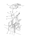
以下、この発明の実施の形態1を図1ないし図6に基づいて説明するが、各図において、同一、または相当部材、部位については同一符号を付して説明する。図1はこの発明の実施の形態1に係わる回路遮断器を示す側面断面図である。図2はこの発明の実施の形態1に係わる回路遮断器における接続端子部を示す部分分解斜視図である。図3はこの発明の実施の形態1に係わる回路遮断器における接続端子部を示す要部側面断面図である。図4はこの発明の実施の形態1に係わる回路遮断器における接続端子部を示す要部拡大側面断面図である。図5はこの発明の実施の形態1に係わる回路遮断器における図4A−A線から見た平面図である。図6はこの発明の実施の形態1に係わる回路遮断器における図5B−B線のベース部を示す断面図である。
Embodiment 1 FIG.
Hereinafter, Embodiment 1 of the present invention will be described with reference to FIGS. 1 to 6. In each figure, the same or equivalent members and parts will be described with the same reference numerals. 1 is a side sectional view showing a circuit breaker according to Embodiment 1 of the present invention. FIG. 2 is a partially exploded perspective view showing a connection terminal portion in the circuit breaker according to Embodiment 1 of the present invention. FIG. 3 is a side sectional view of an essential part showing a connection terminal part in the circuit breaker according to Embodiment 1 of the present invention. 4 is an enlarged side cross-sectional view of a main part showing a connection terminal part in the circuit breaker according to Embodiment 1 of the present invention. 5 is a plan view of the circuit breaker according to the first embodiment of the present invention as viewed from the line 4A-A in FIG. 6 is a cross-sectional view showing a base portion of FIG. 5B-B line in the circuit breaker according to Embodiment 1 of the present invention.

これら各図において、100は回路遮断器であり、大きく分けて、ベース1とカバー2とにより構成される筐体3と、ベース1に収納され、可動接点4を備えた可動接触子5および固定接点6を備えた固定接触子7により構成される開閉機構8と、引き外し機構9と、消弧装置10とにより構成されている。開閉機構8は電路に流れる電流を開閉する。消弧装置10は開閉機構8の可動接点4と固定接点6間に発生するアークを消弧する。なお、ベース1とカバー2はそれぞれ絶縁材料で形成され、ベース1には開閉機構8、引き外し機構、消弧装置10などが収納され、そのベース1をカバー2で覆って回路遮断器100を構成するようにしている。   In these drawings, reference numeral 100 denotes a circuit breaker, which is roughly divided into a housing 3 constituted by a base 1 and a cover 2, a movable contact 5 which is housed in the base 1 and has a movable contact 4, and a fixed. An opening / closing mechanism 8 constituted by a fixed contact 7 provided with a contact 6, a tripping mechanism 9, and an arc extinguishing device 10 are constituted. The opening / closing mechanism 8 opens and closes the current flowing through the electric circuit. The arc extinguishing device 10 extinguishes an arc generated between the movable contact 4 and the fixed contact 6 of the switching mechanism 8. The base 1 and the cover 2 are each formed of an insulating material, and the base 1 contains an opening / closing mechanism 8, a tripping mechanism, an arc extinguishing device 10, etc. The base 1 is covered with the cover 2 to cover the circuit breaker 100. I am trying to configure it.

11は操作ハンドル、12は電源側端子台、13は電源側接続端子であり、一端部は固定接触子7と一体に構成されている。電源側接続端子13は図示しない外部接続導体が接続される。14は電源側端子ねじである。15は負荷側端子台、16は負荷側接続端子、17は負荷側端子ねじである。負荷側接続端子16は図示しない外部接続導体が接続される。   Reference numeral 11 denotes an operation handle, 12 denotes a power supply side terminal block, 13 denotes a power supply side connection terminal, and one end is configured integrally with the fixed contact 7. An external connection conductor (not shown) is connected to the power supply side connection terminal 13. Reference numeral 14 denotes a power supply side terminal screw. 15 is a load side terminal block, 16 is a load side connection terminal, and 17 is a load side terminal screw. An external connection conductor (not shown) is connected to the load side connection terminal 16.

18はベース1の裏面の電源側接続端子13下方側に形成された電源側裏面スタッド装着孔、19はベース1の裏面の負荷側接続端子16下方側に形成された負荷側裏面スタッド装着孔、20は電源側裏面スタッド装着孔18と電源側端子台12表面とを貫通するようにベース1に形成された電源側貫通孔、21は負荷側裏面スタッド装着孔19と負荷側端子台16表面とを貫通するようにベース1に形成された負荷側貫通孔である。   Reference numeral 18 denotes a power supply side rear surface stud mounting hole formed on the lower side of the base 1 on the lower side of the power supply side connection terminal 13, and reference numeral 19 denotes a load side rear surface stud mounting hole formed on the lower side of the base 1 on the lower side of the load side connection terminal 16. Reference numeral 20 denotes a power supply side through hole formed in the base 1 so as to penetrate the power supply side back surface stud mounting hole 18 and the surface of the power supply side terminal block 12, and reference numeral 21 denotes a load side back surface stud mounting hole 19 and the load side terminal block 16 surface. It is a load side through-hole formed in the base 1 so as to pass through.

22は電源側貫通孔20に挿着されるとともにベース1に保持され、電源側裏面スタッド装着孔18を塞ぐ電源側絶縁ブロック、23は負荷側貫通孔21に挿着されるとともにベース1に保持され、負荷側裏面スタッド装着孔19を塞ぐ負荷側絶縁ブロックである。   22 is inserted into the power supply side through hole 20 and held by the base 1, and the power supply side insulating block for closing the power supply side rear surface stud mounting hole 18 is inserted, and 23 is inserted into the load side through hole 21 and held by the base 1. This is a load-side insulating block that closes the load-side back surface stud mounting hole 19.

電源側絶縁ブロック22には例えば相対称位置に突出する係合部22aが形成され、ベース1の電源側貫通孔20部に電源側絶縁ブロック22の係合部22aを保持する保持部1aが電源側貫通孔20と連通して形成されている。電源側絶縁ブロック22の有底部22cを電源側貫通孔20に挿入させ、電源側絶縁ブロック22の係合部22aをベース1の保持部1aに挿入する。電源側絶縁ブロック22の係合部22aの下端面22bがベース1の保持部1aの底部1bに当接することにより、電源側絶縁ブロック22が電源側貫通孔20から抜け落ちないようになっている。電源側絶縁ブロック22は電源側接続端子13とベース1とで挟まれることによりベース1に固定される。   The power supply side insulating block 22 is formed with, for example, an engaging portion 22a protruding in a symmetrical position, and the holding portion 1a that holds the engaging portion 22a of the power supply side insulating block 22 in the power supply side through hole 20 portion of the base 1 is a power source. It is formed in communication with the side through hole 20. The bottomed portion 22 c of the power supply side insulating block 22 is inserted into the power supply side through hole 20, and the engaging portion 22 a of the power supply side insulating block 22 is inserted into the holding portion 1 a of the base 1. Since the lower end surface 22b of the engaging portion 22a of the power supply side insulating block 22 is in contact with the bottom portion 1b of the holding portion 1a of the base 1, the power supply side insulating block 22 is prevented from falling off from the power supply side through hole 20. The power supply side insulating block 22 is fixed to the base 1 by being sandwiched between the power supply side connection terminal 13 and the base 1.

負荷側絶縁ブロック23には例えば相対称位置に突出する係合部23aが形成され、ベース1の負荷側貫通孔21部に負荷側絶縁ブロック23の係合部23aを保持する保持部1aが負荷側貫通孔21と連通して形成されている。負荷側絶縁ブロック23の有底部23cを負荷側貫通孔21に挿入させ、負荷側絶縁ブロック23の係合部23aをベース1の保持部1aに挿入する。負荷側絶縁ブロック23の係合部23aの下端面23bがベース1の保持部1aの底部1bに当接することにより、負荷側絶縁ブロック23が負荷側貫通孔21から抜け落ちないようになっている。負荷側絶縁ブロック23は負荷側接続端子16とベース1とで挟まれることによりベース1に固定される。   The load side insulating block 23 is formed with, for example, an engaging portion 23a that protrudes in a symmetrical position, and the holding portion 1a that holds the engaging portion 23a of the load side insulating block 23 in the load side through hole 21 portion of the base 1 is loaded. It is formed in communication with the side through hole 21. The bottomed portion 23 c of the load side insulating block 23 is inserted into the load side through hole 21, and the engaging portion 23 a of the load side insulating block 23 is inserted into the holding portion 1 a of the base 1. The load-side insulating block 23 is prevented from falling out of the load-side through hole 21 by the lower end surface 23b of the engaging portion 23a of the load-side insulating block 23 coming into contact with the bottom 1b of the holding portion 1a of the base 1. The load-side insulating block 23 is fixed to the base 1 by being sandwiched between the load-side connection terminal 16 and the base 1.

以上のように構成された回路遮断器100においては、表面接続形として使用されている場合を示している。電源側および負荷側も同様に、係合部22aが形成された電源側絶縁ブロック22および係合部23aが形成された負荷側絶縁ブロック23、並びに、電源側絶縁ブロック22を挿通される電源側貫通孔20と電源側絶縁ブロック22の係合部22aが挿入されてその係合部22aを保持するベース1に形成された保持部1a、および負荷側絶縁ブロック23を挿通される負荷側貫通孔21と負荷側絶縁ブロック23の係合部23aが挿入されてその係合部23aを保持するベース1に形成された保持部1aがそれぞれ設けられており、構成は電源側および負荷側も同様である。   In the circuit breaker 100 comprised as mentioned above, the case where it is used as a surface connection type is shown. Similarly, on the power supply side and the load side, the power supply side insulating block 22 formed with the engaging portion 22a, the load side insulating block 23 formed with the engaging portion 23a, and the power supply side inserted through the power supply side insulating block 22 The load part through-hole through which the holding part 1a formed in the base 1 which inserts the engaging part 22a of the through-hole 20 and the power supply side insulating block 22, and holds the engaging part 22a, and the load-side insulating block 23 are inserted. 21 and an engaging portion 23a of the load side insulating block 23 are inserted, and holding portions 1a formed on the base 1 for holding the engaging portion 23a are respectively provided, and the configuration is the same on the power supply side and the load side. is there.

したがって、電源側を主体にして説明する。図2の部分分解斜視図で示すように、ベース1に形成された電源側貫通孔20に電源側絶縁ブロック22の有底部22c側を挿通させ、電源側絶縁ブロック22の係合部22aをベース1に形成された保持部1aに挿入していく。電源側絶縁ブロック22の係合部22aの下端面22bがベース1に形成された保持部1aの底部1bに当接することにより、電源側絶縁ブロック22の挿着が完了する。電源側絶縁ブロック22の係合部22aがベース1に形成された保持部1aの底部1bに受け止められることにより、電源側絶縁ブロック22が電源側貫通孔20から抜け落ちないようになっている。   Therefore, the description will be made mainly on the power supply side. As shown in the partially exploded perspective view of FIG. 2, the bottomed portion 22c side of the power supply side insulating block 22 is inserted into the power supply side through hole 20 formed in the base 1, and the engaging portion 22a of the power supply side insulating block 22 is used as the base. 1 is inserted into the holding portion 1a formed in 1. By inserting the lower end surface 22b of the engaging portion 22a of the power supply side insulating block 22 into contact with the bottom 1b of the holding portion 1a formed on the base 1, the insertion of the power supply side insulating block 22 is completed. The engaging portion 22a of the power supply side insulating block 22 is received by the bottom portion 1b of the holding portion 1a formed on the base 1, so that the power supply side insulating block 22 does not fall out of the power supply side through hole 20.

電源側絶縁ブロック22の電源側貫通孔20への挿着が完了すると、電源側接続端子13を電源側端子台12に設置し、表面側外部接続端子(図示せず)と電源側接続端子13を電源側端子ねじ14により締め付けられて接続される。電源側端子ねじ14の締め付けによって電源側接続端子13と表面側外部接続端子とが接続されることにより、電源側絶縁ブロック22は電源側接続端子13とベース1とで挟まれることによりベース1に固定される。   When the insertion of the power supply side insulating block 22 into the power supply side through hole 20 is completed, the power supply side connection terminal 13 is installed on the power supply side terminal block 12, and the front surface side external connection terminal (not shown) and the power supply side connection terminal 13 are installed. Are tightened by the power supply side terminal screw 14 and connected. By connecting the power supply side connection terminal 13 and the front surface side external connection terminal by tightening the power supply side terminal screw 14, the power supply side insulating block 22 is sandwiched between the power supply side connection terminal 13 and the base 1, thereby being attached to the base 1. Fixed.

また、図4に示すように、電源側絶縁ブロック22は有底部22cを有し、その有底部22cの上方には空間部22dが形成され、電源側端子ねじ14のねじ部14aの先端部と当たらないように空間距離で配設されている。   As shown in FIG. 4, the power supply side insulating block 22 has a bottomed portion 22 c, and a space 22 d is formed above the bottomed portion 22 c, and the tip of the screw portion 14 a of the power supply side terminal screw 14 and It is arranged at a spatial distance so as not to hit.

さらに、電源側絶縁ブロック22は例えば図2、図4、図5に示すように円筒状に形成され、電源側貫通孔20は例えば図2、図4〜図6に示すように円状に形成されている。これら電源側絶縁ブロック22、電源側貫通孔20は円形状に限定されるものではなく、四角形状の多角形状からなる場合も同様の効果を奏する。   Furthermore, the power supply side insulating block 22 is formed in a cylindrical shape as shown in FIGS. 2, 4 and 5, for example, and the power supply side through hole 20 is formed in a circular shape as shown in FIGS. 2 and 4 to 6, for example. Has been. The power supply side insulating block 22 and the power supply side through hole 20 are not limited to a circular shape, and the same effect can be obtained when the power supply side insulating block 22 and the power supply side through hole 20 are formed in a quadrangular polygonal shape.

以上のように、表面接続形として使用されている回路遮断器100においては、電源側絶縁ブロック22を取り付けたことにより、電源側接続端子13の電源側端子ねじ14のねじ部14a先端と盤面との絶縁距離を十分に確保することができるので、絶縁特性に優れた回路遮断器を得ることができる。   As described above, in the circuit breaker 100 used as the surface connection type, by attaching the power supply side insulating block 22, the tip of the screw portion 14a of the power supply side terminal screw 14 of the power supply side connection terminal 13 and the board surface Since a sufficient insulation distance can be secured, a circuit breaker having excellent insulation characteristics can be obtained.

なお、電源側を主体に説明したが、負荷側においても電源側と同様の構成をとっており、詳細な説明は省略するが同様の効果を奏する。   Although the description has been made mainly on the power supply side, the load side has the same configuration as that on the power supply side, and the same effect is obtained although the detailed description is omitted.

実施の形態2.
上述した実施の形態1においては、電源側絶縁ブロック22および負荷側絶縁ブロック23を取り付けた回路遮断器100であり、表面接続形として使用されている場合について述べたが、この実施の形態2は表面接続形から裏面接続形に改造する製造方法であり、図7および図8に基づいて説明する。図7はこの発明の実施の形態2に係わる回路遮断器を示す側面図である。図8はこの発明の実施の形態2に係わる回路遮断器における接続端子部を示す要部拡大側面断面図である。
Embodiment 2. FIG.
In the above-described first embodiment, the circuit breaker 100 to which the power-side insulating block 22 and the load-side insulating block 23 are attached has been described as being used as a surface connection type. This is a manufacturing method for remodeling from the front connection type to the back connection type, and will be described with reference to FIGS. FIG. 7 is a side view showing a circuit breaker according to Embodiment 2 of the present invention. FIG. 8: is a principal part expanded side sectional view which shows the connection terminal part in the circuit breaker concerning Embodiment 2 of this invention.

上述した実施の形態1のように、表面接続形として使用されている回路遮断器100から裏面接続形に改造する方法について説明する。   A method of remodeling the circuit breaker 100 used as the front surface connection type to the back surface connection type as in the first embodiment will be described.

まず、電源側端子ねじ14を緩めて取り外して表面側外部接続端子(図示せず)を取り外し、電源側接続端子13を電源側端子台12から離間させて電源側絶縁ブロック22をベース1の電源側貫通孔20から取り出す。同様に、負荷側端子ねじ17を緩めて取り外して表面側外部接続端子(図示せず)を取り外し、負荷側接続端子16を負荷側端子台15から離間させて負荷側絶縁ブロック23をベース1の負荷側貫通孔21から取り出す。   First, the power supply side terminal screw 14 is loosened and removed to remove the surface side external connection terminal (not shown), the power supply side connection terminal 13 is separated from the power supply side terminal block 12, and the power supply side insulation block 22 is connected to the power supply of the base 1. Take out from the side through hole 20. Similarly, the load-side terminal screw 17 is loosened and removed to remove the surface-side external connection terminal (not shown), the load-side connection terminal 16 is separated from the load-side terminal block 15, and the load-side insulating block 23 is attached to the base 1. Take out from the load side through hole 21.

次いで、電源側絶縁ブロック22、負荷側絶縁ブロック23を電源側貫通孔20、負荷側貫通孔21から取り出した後、電源側接続端子13、負荷側接続端子16をそれぞれ電源側端子台12、負荷側端子台15に設置する。   Next, after the power supply side insulation block 22 and the load side insulation block 23 are taken out from the power supply side through hole 20 and the load side through hole 21, the power supply side connection terminal 13 and the load side connection terminal 16 are respectively connected to the power supply side terminal block 12 and the load. Installed on the side terminal block 15.

そして、電源側裏面スタッド24の一端側24a、負荷側裏面スタッド25の一端側25aを電源側裏面スタッド装着孔18、負荷側裏面スタッド装着孔19並びに電源側貫通孔20、負荷側貫通孔21をそれぞれ挿通する。電源側裏面スタッド24の一端側24a、負荷側裏面スタッド25の一端側25aにはそれぞれねじ穴24a1、ねじ穴25a1(図示せず)が形成されている。これら電源側裏面スタッド24の一端側24aのねじ穴24a1、負荷側裏面スタッド25の一端側25aのねじ穴25a1(図示せず)に電源側接続端子13、負荷側接続端子16を螺入した電源側端子ねじ14のねじ部14a、負荷側端子ねじ17のねじ部(図示せず)が螺入されて締め付けられて電源側接続端子13、負荷側接続端子16と接続される。   Then, one end side 24a of the power supply side back surface stud 24 and one end side 25a of the load side back surface stud 25 are connected to the power supply side back surface stud mounting hole 18, the load side back surface stud mounting hole 19, the power supply side through hole 20, and the load side through hole 21. Insert each one. A screw hole 24a1 and a screw hole 25a1 (not shown) are formed in one end side 24a of the power supply side back surface stud 24 and one end side 25a of the load side back surface stud 25, respectively. A power supply in which the power supply side connection terminal 13 and the load side connection terminal 16 are screwed into the screw hole 24a1 on one end side 24a of the power supply side rear surface stud 24 and the screw hole 25a1 (not shown) on one end side 25a of the load side rear surface stud 25. The screw portion 14 a of the side terminal screw 14 and the screw portion (not shown) of the load side terminal screw 17 are screwed and tightened to be connected to the power supply side connection terminal 13 and the load side connection terminal 16.

電源側裏面スタッド24の他端側24b、負荷側裏面スタッド25の他端側25bには外部接続導体(図示せず)が接続される。また、電源側裏面スタッド24、負荷側裏面スタッド25のベース1裏面部にはそれぞれ絶縁菅26、絶縁菅27が設けられており、絶縁特性の向上が図られている。なお、電源側裏面スタッド24の取り付け位置に対して負荷側裏面スタッド25の取り付け位置は例えば90度回転した位置となっている。   An external connection conductor (not shown) is connected to the other end side 24 b of the power supply side rear surface stud 24 and the other end side 25 b of the load side rear surface stud 25. Further, an insulating rod 26 and an insulating rod 27 are provided on the back surface of the base 1 of the power supply side back surface stud 24 and the load side back surface stud 25, respectively, so that the insulation characteristics are improved. The mounting position of the load-side back surface stud 25 is, for example, a position rotated by 90 degrees with respect to the mounting position of the power-side back surface stud 24.

以上のように、電源側端子ねじ14、負荷側端子ねじ17を取り外して電源側絶縁ブロック22、負荷側絶縁ブロック23を電源側貫通孔20、負荷側貫通孔21から取り出すことにより、電源側裏面スタッド24、負荷側裏面スタッド25を電源側接続端子13、負荷側接続端子16と接続させることができるので、表面接続形から裏面接続形へ簡易に改造することができる。また、これらと逆に、裏面接続形から表面接続形においても逆動作をすることにより簡易に改造することができる。   As described above, the power-side terminal screw 14 and the load-side terminal screw 17 are removed, and the power-side insulating block 22 and the load-side insulating block 23 are taken out from the power-side through hole 20 and the load-side through hole 21, thereby Since the stud 24 and the load side back surface stud 25 can be connected to the power source side connection terminal 13 and the load side connection terminal 16, it can be easily modified from the front surface connection type to the back surface connection type. On the contrary, the reverse connection type to the front side connection type can be easily modified by performing the reverse operation.

実施の形態3.
この発明の実施の形態3に係る回路遮断器を図9および図10に基づいて説明する。図9はこの発明の実施の形態3に係わる回路遮断器における絶縁ブロックを示す斜視図である。図10はこの発明の実施の形態3に係わる回路遮断器における絶縁ブロックの取り付け状態を示す断面図である。
Embodiment 3 FIG.
A circuit breaker according to Embodiment 3 of the present invention will be described with reference to FIGS. 9 is a perspective view showing an insulating block in a circuit breaker according to Embodiment 3 of the present invention. FIG. 10 is a cross-sectional view showing a state where the insulating block is attached to the circuit breaker according to Embodiment 3 of the present invention.

この実施の形態3の回路遮断器においては、絶縁ブロック28は円筒状の係合部28aとした場合を示しており、電源側および負荷側に同一構成として使用される。絶縁ブロック28を電源側に使用した場合を図10に基づいて説明する。   In the circuit breaker according to the third embodiment, the insulating block 28 is a cylindrical engaging portion 28a, and is used as the same configuration on the power supply side and the load side. A case where the insulating block 28 is used on the power supply side will be described with reference to FIG.

ベース1に電源側貫通孔20と連通して形成される保持部101aは絶縁ブロック28の係合部28aの形状と同様となるよう円形状に構成されている。ベース1に形成された電源側貫通孔20に絶縁ブロック28の有底部28c側を挿通させ、絶縁ブロック28の係合部28aをベース1に形成された保持部101aに挿入していく。絶縁ブロック28の係合部28aの下端面28bがベース1に形成された保持部101aの底部101bに当接することにより、絶縁ブロック28の挿着が完了する。絶縁ブロック28の係合部28aがベース1に形成された保持部101aの底部101bに受け止められることにより、絶縁ブロック28が電源側貫通孔20から抜け落ちないようになっている。   The holding portion 101a formed in the base 1 so as to communicate with the power supply side through hole 20 is formed in a circular shape so as to be similar to the shape of the engaging portion 28a of the insulating block 28. The bottomed portion 28 c side of the insulating block 28 is inserted into the power supply side through hole 20 formed in the base 1, and the engaging portion 28 a of the insulating block 28 is inserted into the holding portion 101 a formed in the base 1. When the lower end surface 28b of the engaging portion 28a of the insulating block 28 comes into contact with the bottom 101b of the holding portion 101a formed on the base 1, the insertion of the insulating block 28 is completed. Since the engaging portion 28 a of the insulating block 28 is received by the bottom portion 101 b of the holding portion 101 a formed on the base 1, the insulating block 28 is prevented from falling off from the power supply side through hole 20.

また、絶縁ブロック28は有底部28cを有し、その有底部28cの上方には空間部28dが形成され、電源側端子ねじ14のねじ部14aの先端部と当たらないように空間距離で配設されている。   The insulating block 28 has a bottomed portion 28c. A space portion 28d is formed above the bottomed portion 28c, and is arranged at a spatial distance so as not to contact the tip of the screw portion 14a of the power supply side terminal screw 14. Has been.

なお、絶縁ブロック28を電源側貫通孔20に挿着する場合について述べたが、図示はしないが絶縁ブロック28を負荷側貫通孔21に挿着する場合も上述した実施の形態3と同様に行われる。   Although the case where the insulating block 28 is inserted into the power supply side through hole 20 has been described, although not shown, the case where the insulating block 28 is inserted into the load side through hole 21 is the same as in the third embodiment. Is called.

以上のように、この実施の形態3においても、上述した実施の形態1と同様の効果を奏する。また、絶縁ブロック28は円筒状に限定されるものではなく、四角形状の多角形状からなる場合も同様の効果を奏する。   As described above, this third embodiment also has the same effects as those of the first embodiment described above. The insulating block 28 is not limited to a cylindrical shape, and the same effect can be obtained when the insulating block 28 is formed of a quadrangular polygonal shape.

実施の形態4.
この発明の実施の形態4に係る回路遮断器を図11および図12に基づいて説明する。図11はこの発明の実施の形態4に係わる回路遮断器における絶縁ブロックを示す斜視図である。図12はこの発明の実施の形態4に係わる回路遮断器における絶縁ブロックの取り付け状態を示す断面図である。
Embodiment 4 FIG.
A circuit breaker according to Embodiment 4 of the present invention will be described with reference to FIGS. 11 and 12. FIG. 11 is a perspective view showing an insulating block in a circuit breaker according to Embodiment 4 of the present invention. FIG. 12 is a cross-sectional view showing an attachment state of an insulating block in a circuit breaker according to Embodiment 4 of the present invention.

この実施の形態4の回路遮断器においては、絶縁ブロック29はテーパ状の円筒状からなり、電源側貫通孔20および負荷側貫通孔21の孔径寸法より大径寸法を有する係合部29aとした場合を示しており、電源側および負荷側に同一構成として使用される。絶縁ブロック29を電源側に使用した場合を図12に基づいて説明する。   In the circuit breaker according to the fourth embodiment, the insulating block 29 has a tapered cylindrical shape, and is an engagement portion 29a having a diameter larger than the diameters of the power supply side through hole 20 and the load side through hole 21. The case is shown, and the same configuration is used on the power supply side and the load side. A case where the insulating block 29 is used on the power supply side will be described with reference to FIG.

ベース1に電源側貫通孔20と連通して形成される保持部102aは絶縁ブロック29のテーパ状の円筒状からなる係合部29aの形状と同様となるようテーパ状の円形状に構成されている。ベース1に形成された電源側貫通孔20に絶縁ブロック29の有底部29c側を挿通させ、絶縁ブロック29の係合部29aをベース1に形成された保持部102aに挿入していく。絶縁ブロック29の係合部29aのテーパ部がベース1に形成された保持部102aのテーパ部に当接することにより、絶縁ブロック29の挿着が完了する。絶縁ブロック29の係合部29aのテーパ部がベース1に形成された保持部102aのテーパ部に受け止められることにより、絶縁ブロック29が電源側貫通孔20から抜け落ちないようになっている。   The holding portion 102a formed in the base 1 in communication with the power supply side through hole 20 is formed in a tapered circular shape so as to be similar to the shape of the tapered cylindrical engaging portion 29a of the insulating block 29. Yes. The bottomed portion 29 c side of the insulating block 29 is inserted into the power supply side through hole 20 formed in the base 1, and the engaging portion 29 a of the insulating block 29 is inserted into the holding portion 102 a formed in the base 1. The insertion of the insulating block 29 is completed when the tapered portion of the engaging portion 29 a of the insulating block 29 abuts on the tapered portion of the holding portion 102 a formed on the base 1. The tapered portion of the engaging portion 29 a of the insulating block 29 is received by the tapered portion of the holding portion 102 a formed on the base 1, so that the insulating block 29 does not fall out of the power supply side through hole 20.

また、絶縁ブロック29は有底部29cを有し、その有底部29cの上方には空間部29dが形成され、電源側端子ねじ14のねじ部14aの先端部と当たらないように空間距離で配設されている。   The insulating block 29 has a bottomed portion 29c, and a space portion 29d is formed above the bottomed portion 29c, and is disposed at a spatial distance so as not to contact the tip of the screw portion 14a of the power supply side terminal screw 14. Has been.

なお、絶縁ブロック29を電源側貫通孔20に挿着する場合について述べたが、図示はしないが絶縁ブロック29を負荷側貫通孔21に挿着する場合も上述した実施の形態4と同様に行われる。   Although the case where the insulating block 29 is inserted into the power supply side through hole 20 has been described, although not shown, the case where the insulating block 29 is inserted into the load side through hole 21 is the same as in the fourth embodiment. Is called.

以上のように、この実施の形態4においても、上述した実施の形態1および実施の形態3と同様の効果を奏する。また、絶縁ブロック29はテーパ状の円筒状に限定されるものではなく、四角形状の多角形状でテーパ状からなる場合も同様の効果を奏する。   As described above, also in the fourth embodiment, the same effects as in the first and third embodiments described above are obtained. Further, the insulating block 29 is not limited to a tapered cylindrical shape, and the same effect can be obtained when the insulating block 29 is a quadrangular polygonal shape and is tapered.

この発明は、接続端子のねじ部先端と盤面との絶縁距離が十分に確保できる回路遮断器の実現に好適である。   The present invention is suitable for realizing a circuit breaker that can secure a sufficient insulation distance between the tip of the screw portion of the connection terminal and the board surface.

1 ベース
1a 保持部
2 カバー
3 筐体
8 開閉機構
12 電源側端子台
13 電源側接続端子
14 電源側端子ねじ
15 負荷側端子台
16 負荷側接続端子
17 負荷側端子ねじ
18 電源側裏面スタッド装着孔
19 負荷側裏面スタッド装着孔
20 電源側貫通孔
21 負荷側貫通孔
22 電源側絶縁ブロック
22a 係合部
22c 有底部
23 負荷側絶縁ブロック
23a 係合部
23c 有底部
24 電源側裏面スタッド
25 負荷側裏面スタッド
28 絶縁ブロック
28a 係合部
28c 有底部
29 絶縁ブロック
29a 係合部
29c 有底部
100 回路遮断器
101a 保持部
102a 保持部
DESCRIPTION OF SYMBOLS 1 Base 1a Holding part 2 Cover 3 Case 8 Opening / closing mechanism 12 Power supply side terminal block 13 Power supply side connection terminal 14 Power supply side terminal screw 15 Load side terminal block 16 Load side connection terminal 17 Load side terminal screw 18 Power supply side back surface stud attachment hole 19 Load side rear surface stud mounting hole 20 Power source side through hole 21 Load side through hole 22 Power source side insulating block 22a Engaging portion 22c Bottomed portion 23 Load side insulating block 23a Engaging portion 23c Bottomed portion 24 Power side rear surface stud 25 Load side rear surface Stud 28 Insulating block 28a Engaging portion 28c Bottomed portion 29 Insulating block 29a Engaging portion 29c Bottomed portion 100 Circuit breaker 101a Holding portion 102a Holding portion

Claims (2)

電路に流れる電流を開閉する開閉機構と、絶縁材料で形成され、前記開閉機構を収納するベースと、絶縁材料で形成され、前記ベースを覆い前記ベースとともに筐体を構成するカバーと、前記ベースの端子台に配設され、外部接続導体が接続される接続端子とを備える回路遮断器において、前記ベースの裏面の前記接続端子下方側に形成された裏面スタッド装着孔と、前記裏面スタッド装着孔と前記端子台表面とを貫通するように前記ベースに形成された貫通孔と、前記貫通孔に挿着されるとともに前記ベースに保持され、前記裏面スタッド装着孔を塞ぐ絶縁ブロックとを設け、前記絶縁ブロックには有底部が設けられているとともに前記ベースに保持される係合部を設け、前記ベースには前記絶縁ブロックの前記係合部を保持する保持部が設けられたことを特徴とする回路遮断器。 An opening / closing mechanism that opens and closes an electric current flowing through the electric circuit; a base that is formed of an insulating material and houses the opening / closing mechanism; a cover that is formed of an insulating material and covers the base and forms a housing together with the base; A circuit breaker provided on a terminal block and connected to an external connection conductor, wherein the back surface stud mounting hole formed on the back surface of the base on the lower side of the connection terminal , and the back surface stud mounting hole and a through-hole formed in the base so as to penetrate the said terminal block surface, the is while being inserted into the through hole is held in the base, set an insulating block to close the backside stud mounting hole The insulating block has a bottomed portion and is provided with an engaging portion held by the base, and the base holds the engaging portion of the insulating block. Circuit breaker, characterized in that is provided. カバーとともに筐体を構成するベースの裏面の接続端子の下方側に形成された裏面スタッド装着孔に裏面スタッドを装着するとき、前記ベースに形成された貫通孔に挿着され前記裏面スタッド装着孔を塞ぐ絶縁ブロックを取り外し、前記裏面スタッドを前記裏面スタッド装着孔および前記貫通孔を挿通させて前記接続端子に端子ねじにより接続させるようにしたことを特徴とする回路遮断器の製造方法。 When attaching the back stud to the back stud mounting hole formed on the lower side of the connection terminal on the back of the base constituting the housing together with the cover, the back stud mounting hole is inserted into the through hole formed in the base. closing remove the insulating block, producing how the circuit breaker being characterized in that so as to be connected by the terminal screw to the connection terminals of the back stud is passed through the backside stud mounting hole and the through hole.
JP2010235493A 2010-10-20 2010-10-20 Circuit breaker and manufacturing method thereof Expired - Fee Related JP5538650B2 (en)

Priority Applications (2)

Application Number Priority Date Filing Date Title
JP2010235493A JP5538650B2 (en) 2010-10-20 2010-10-20 Circuit breaker and manufacturing method thereof
CN201110041681.2A CN102456521B (en) 2010-10-20 2011-02-21 Circuit breaker

Applications Claiming Priority (1)

Application Number Priority Date Filing Date Title
JP2010235493A JP5538650B2 (en) 2010-10-20 2010-10-20 Circuit breaker and manufacturing method thereof

Publications (3)

Publication Number Publication Date
JP2012089372A JP2012089372A (en) 2012-05-10
JP2012089372A5 JP2012089372A5 (en) 2013-07-25
JP5538650B2 true JP5538650B2 (en) 2014-07-02

Family

ID=46039581

Family Applications (1)

Application Number Title Priority Date Filing Date
JP2010235493A Expired - Fee Related JP5538650B2 (en) 2010-10-20 2010-10-20 Circuit breaker and manufacturing method thereof

Country Status (2)

Country Link
JP (1) JP5538650B2 (en)
CN (1) CN102456521B (en)

Families Citing this family (4)

* Cited by examiner, † Cited by third party
Publication number Priority date Publication date Assignee Title
CN104979141B (en) * 2014-04-08 2017-09-26 三菱电机株式会社 Breaker
JP6217517B2 (en) * 2014-04-08 2017-10-25 三菱電機株式会社 Circuit breaker
JP6409694B2 (en) * 2015-06-29 2018-10-24 三菱電機株式会社 Circuit breaker
CN108511276A (en) * 2018-05-16 2018-09-07 河南森源电气股份有限公司 A kind of breaker of plastic casing and its felt pad

Family Cites Families (6)

* Cited by examiner, † Cited by third party
Publication number Priority date Publication date Assignee Title
JPS5593926U (en) * 1978-12-22 1980-06-28
JPH0629875Y2 (en) * 1985-10-14 1994-08-10 三菱電機株式会社 Circuit breaker
JPH02111044U (en) * 1989-02-22 1990-09-05
JPH0567424A (en) * 1991-05-09 1993-03-19 Fuji Electric Co Ltd Circuit breaker
JP3407017B2 (en) * 1997-08-20 2003-05-19 三菱電機株式会社 Circuit breaker
US6636133B2 (en) * 2001-09-14 2003-10-21 Square D Company PTC terminals

Also Published As

Publication number Publication date
CN102456521B (en) 2014-12-10
CN102456521A (en) 2012-05-16
JP2012089372A (en) 2012-05-10

Similar Documents

Publication Publication Date Title
JP4836919B2 (en) Plug-in circuit breaker
JP5337565B2 (en) Ground wire relay terminal block and distribution board equipped with the same
JP5538650B2 (en) Circuit breaker and manufacturing method thereof
JP6113867B2 (en) Breaker
JP2016033890A (en) DC breaker
CN101958212B (en) Receptacle type residual current circuit breaker
CN104380551A (en) An electrically insulating shell, an electrically insulating device comprising such insulating shell, and related switchgear panel
JP2020024961A (en) Circuit breaker and distribution board
JP2012089372A5 (en)
JP5618919B2 (en) Switch insertion device
CN102405566B (en) Electric terminal for leading a conductor through a wall
WO2017041707A1 (en) Surge protection device base
JP2020054102A (en) Distribution board
JP2014057445A (en) Connection box
JP2007318875A (en) Distribution panel for housing
TWI541851B (en) Circuit breaker
JP6984029B2 (en) Electronic trip device for molded case circuit breaker
RU2666748C2 (en) Double wall socket
JP2019067630A (en) Plug device and power distribution system
JP7346127B2 (en) plug-in breaker
JP5202424B2 (en) Circuit breaker
JP5922426B2 (en) Circuit breaker
KR200383042Y1 (en) Outlet for distribution switchboard
JP5908300B2 (en) Circuit breaker
JP6041197B2 (en) Connection box

Legal Events

Date Code Title Description
A521 Request for written amendment filed

Free format text: JAPANESE INTERMEDIATE CODE: A523

Effective date: 20130607

A621 Written request for application examination

Free format text: JAPANESE INTERMEDIATE CODE: A621

Effective date: 20130607

A977 Report on retrieval

Free format text: JAPANESE INTERMEDIATE CODE: A971007

Effective date: 20140115

A131 Notification of reasons for refusal

Free format text: JAPANESE INTERMEDIATE CODE: A131

Effective date: 20140204

A521 Request for written amendment filed

Free format text: JAPANESE INTERMEDIATE CODE: A523

Effective date: 20140314

TRDD Decision of grant or rejection written
A01 Written decision to grant a patent or to grant a registration (utility model)

Free format text: JAPANESE INTERMEDIATE CODE: A01

Effective date: 20140401

R151 Written notification of patent or utility model registration

Ref document number: 5538650

Country of ref document: JP

Free format text: JAPANESE INTERMEDIATE CODE: R151

A61 First payment of annual fees (during grant procedure)

Free format text: JAPANESE INTERMEDIATE CODE: A61

Effective date: 20140429

R250 Receipt of annual fees

Free format text: JAPANESE INTERMEDIATE CODE: R250

R250 Receipt of annual fees

Free format text: JAPANESE INTERMEDIATE CODE: R250

R250 Receipt of annual fees

Free format text: JAPANESE INTERMEDIATE CODE: R250

R250 Receipt of annual fees

Free format text: JAPANESE INTERMEDIATE CODE: R250

R250 Receipt of annual fees

Free format text: JAPANESE INTERMEDIATE CODE: R250

R250 Receipt of annual fees

Free format text: JAPANESE INTERMEDIATE CODE: R250

LAPS Cancellation because of no payment of annual fees