JP5517127B2 - Terahertz electromagnetic wave generator - Google Patents
Terahertz electromagnetic wave generator Download PDFInfo
- Publication number
- JP5517127B2 JP5517127B2 JP2010098684A JP2010098684A JP5517127B2 JP 5517127 B2 JP5517127 B2 JP 5517127B2 JP 2010098684 A JP2010098684 A JP 2010098684A JP 2010098684 A JP2010098684 A JP 2010098684A JP 5517127 B2 JP5517127 B2 JP 5517127B2
- Authority
- JP
- Japan
- Prior art keywords
- substrate
- line
- photoconductive
- terahertz electromagnetic
- electromagnetic wave
- Prior art date
- Legal status (The legal status is an assumption and is not a legal conclusion. Google has not performed a legal analysis and makes no representation as to the accuracy of the status listed.)
- Active
Links
Images


Landscapes
- Details Of Aerials (AREA)
- Aerials With Secondary Devices (AREA)
Description
この発明は、テラヘルツ電磁波を効率的に発生することのできるテラヘルツ電磁波発生装置に関する。 The present invention relates to a terahertz electromagnetic wave generator that can efficiently generate terahertz electromagnetic waves.
テラヘルツ電磁波は周波数が0.1〜10THz(波長が30μm〜3000μm)の電磁波とされており、波長が赤外〜遠赤外領域とほぼ一致する。テラヘルツ電磁波は、「光」と「ミリ波」に挟まれた周波数領域に存在しているため、テラヘルツ電磁波は、光と同様に高い空間分解能でものを見分ける能力と、ミリ波と同様の物質を透過する能力を併せ持っている。テラヘルツ波帯はこれまで未開拓電磁波であったが、この周波数帯の電磁波の特徴を生かした時間領域分光、イメージング及びトモグラフィーによる材料のキャラクタリゼーション、環境計測、生物や医学への応用などが検討されてきている。テラヘルツ電磁波の発生は、物質透過性と直進性を兼ね備えるためX線に替わる安全かつ革新的なイメージングや数100Gbps級の超高速無線通信が可能となる。特に半導体製作による光伝導アンテナは、製作が容易でテラヘルツ時間領域分光法などで既に多くの実績を有している。 The terahertz electromagnetic wave is an electromagnetic wave having a frequency of 0.1 to 10 THz (wavelength is 30 μm to 3000 μm), and the wavelength substantially coincides with the infrared to far infrared region. Since terahertz electromagnetic waves exist in a frequency region sandwiched between “light” and “millimeter waves”, terahertz electromagnetic waves have the same ability to distinguish at high spatial resolution as light, and the same substances as millimeter waves. It also has the ability to penetrate. The terahertz wave band was an undeveloped electromagnetic wave so far, but time domain spectroscopy using the characteristics of the electromagnetic wave in this frequency band, characterization of materials by imaging and tomography, environmental measurement, application to organisms and medicine, etc. were studied. It is coming. Since the generation of terahertz electromagnetic waves has both material permeability and straightness, safe and innovative imaging instead of X-rays and ultra-high-speed wireless communication of several hundred Gbps class are possible. In particular, photoconductive antennas manufactured by semiconductors are easy to manufacture and have already been proven in terahertz time domain spectroscopy.
従来のテラヘルツ電磁波発生装置とされる光伝導アンテナ100の一構成例を図17に示す。
図17に示す光伝導アンテナ100は、GaAs(Gallium Arsenide)基板とされる第1基板111の一面に光伝導膜110とされる低温成長GaAs膜を形成し、光伝導膜110の上に平行伝送線路からなる導電性の第1ライン112aおよび第2ライン112bを蒸着等により形成している。GaAsは、Ga(ガリウム)とAs(砒素)の化合物からなる化合物半導体である。第1ライン112aおよび第2ライン112bのほぼ中央には、対向部112cで対向する導電性の第1エレメント113aおよび第2エレメント113bが形成されている。対向部112cの間隔は、例えば数μm程度とされる。このような構成の光伝導アンテナ100において、第1ライン112aと第2ライン112bとの間に直流のバイアス電圧Ecを印加する。この状態では、第1ライン112aと第2ライン112bとの間は対向部112cにより絶縁されているため電流は流れない。そこで、光源114から10-15秒程度のフェムト秒パルスレーザ光を対向部112cに照射する。パルスレーザ光を対向部112cに照射すると、対向部112cにおける光伝導膜110中に光導電効果により自由キャリアが生じ、この自由キャリアがバイアス電圧Ecにより加速されることにより、第1エレメント113aおよび第2エレメント113bを介して第1ライン112aと第2ライン112b間にサブピコ秒(10-12秒)程度のパルス状の電流が流れる。このパルス状の電流によって第1エレメント113aおよび第2エレメント113bが励振されて、テラヘルツ電磁波が第1エレメント113aおよび第2エレメント113bから放射される。なお、第1エレメント113aおよび第2エレメント113bはダイポールアンテナ113として作用する。
One structural example of the
In the
図17に示す従来の光伝導アンテナ100では、テラヘルツ電磁波は光伝導膜110および第1基板111を介してz軸方向に放射される。そこで、従来の光伝導アンテナ100におけるy−z面(E面)とx−z面(H面)の放射指向特性を図18に示す。図18を参照すると、y−z面(E面)の放射指向特性においては、約±16°方向の放射界が高くされているが、z軸方向とされる0°方向(正面方向)のメインビームの放射界は小さくなっている。さらに、±180°方向にはほぼ放射されない。また、x−z面(H面)の放射指向特性においては、z軸方向とされる0°方向(正面方向)にメインビームが放射され,メインビームの両側とされる約±30°方向にサイドローブが放射されている。この場合のメインビームおよびサイドローブの最大放射界はほぼ同様とされているが、y−z面(E面)の最大放射界より小さくなっている。また、±180°方向にはほぼ放射されない。
In the conventional
このように、従来の光伝導アンテナ100においては正面方向の放射利得が低下している。この原因は、低温成長GaAsを材料とする光伝導膜110の比誘電率εrが約13の高誘電率とされて、光伝導膜110で損失を受けていること、および、第1基板11および光伝導膜110の境界面において反射していることが原因と考えられる。しかしながら、光伝導膜110の材料としては、光源114からレーザ光が照射された際に生じる自由電子のキャリア寿命が短いと共にキャリア移動度が大きい材料とする必要があり、このような材料の比誘電率は、一般的に高いことが知られている。すると、光伝導膜を有することが必須の構成要件とされる光伝導アンテナでは、放射利得等のアンテナ性能を向上することができないという問題点があった。
そこで、本発明は、光伝導膜を有していてもアンテナ性能を向上することができるテラヘルツ電磁波発生装置を提供することを目的としている。
Thus, in the conventional
Accordingly, an object of the present invention is to provide a terahertz electromagnetic wave generator that can improve antenna performance even if it has a photoconductive film.
上記目的を達成するために、本発明の第1実施例のテラヘルツ電磁波発生装置は、金属板と、該金属板上に配置され、光が照射された際に自由電子が生じる比誘電率εr1の光伝導層が表面に形成された絶縁性の第1基板と、前記金属板上に前記第1基板の横に隣接して密着するよう配置された比誘電率εr2の絶縁性の第2基板と、該第2基板の表面に形成された導電性のダイポールアンテナのエレメントと、該ダイポールアンテナの給電点から引き出され、前記第2基板の表面から前記第1基板における前記光伝導層上にわたって形成された第1ラインおよび第2ラインと、前記光伝導層上に形成されている前記第1ラインと前記第2ラインの端部が所定の間隔で対向している対向部と、該対向部にパルス状の光を照射する光源と、前記第1ラインと前記第2ラインとの間に電源を印加するバイアス電源とを備え、比誘電率εr1>比誘電率εr2とされていることを最も主要な特徴としている。
また、本発明の第2実施例のテラヘルツ電磁波発生装置は、光が照射された際に自由電子が生じる光伝導層が一面に形成され、他面に金属層が形成された比誘電率εr1の絶縁性の第1基板と、前記金属層上に配置された比誘電率εr2の絶縁性の第2基板と、該第2基板の表面に形成された導電性のダイポールアンテナのエレメントと、該ダイポールアンテナの給電点から引き出され、前記第2の基板、前記金属層、前記第1の基板および前記光伝導層を貫通して、前記光伝導層上に形成された第1ラインおよび第2ラインと、前記光伝導層上に形成されている前記第2ラインに形成された切欠部と、該切欠部にパルス状の光を照射する光源と、前記第1ラインの端部と、前記第2ラインの端部との間に印加されたバイアス電源とを備え、比誘電率εr1>比誘電率εr2とされていることを最も主要な特徴としている。
In order to achieve the above object, a terahertz electromagnetic wave generator according to a first embodiment of the present invention has a metal plate and a relative permittivity εr1 that is arranged on the metal plate and generates free electrons when irradiated with light. An insulative first substrate having a photoconductive layer formed on the surface thereof; an insulative second substrate having a relative dielectric constant εr2 disposed on the metal plate so as to be in close contact with the side of the first substrate; An element of a conductive dipole antenna formed on the surface of the second substrate, and drawn from a feeding point of the dipole antenna , and formed from the surface of the second substrate over the photoconductive layer of the first substrate. A first line and a second line; a counter part where ends of the first line and the second line formed on the photoconductive layer oppose each other at a predetermined interval; and a pulse in the counter part. A light source for irradiating a shaped light; The main feature is that a bias power source for applying a power source is provided between one line and the second line, and the relative permittivity εr1> relative permittivity εr2.
The terahertz electromagnetic wave generator according to the second embodiment of the present invention has a relative permittivity εr1 in which a photoconductive layer that generates free electrons when irradiated with light is formed on one surface and a metal layer is formed on the other surface. An insulating first substrate; an insulating second substrate having a relative dielectric constant εr2 disposed on the metal layer; an element of a conductive dipole antenna formed on a surface of the second substrate; and the dipole A first line and a second line which are drawn from the feeding point of the antenna and pass through the second substrate, the metal layer, the first substrate, and the photoconductive layer, and are formed on the photoconductive layer; A notch formed in the second line formed on the photoconductive layer, a light source for irradiating the notch with pulsed light, an end of the first line, and the second line And a bias power source applied between the ends of the The main feature is that the dielectric constant εr1> the relative dielectric constant εr2.
本発明によれば、パルス状の光が照射される光伝導層上に形成されている対向部あるいは切欠部が、第2基板上に形成されているダイポールアンテナの給電部として作用するようになり、対向部あるいは切欠部から給電されたダイポールアンテナからテラヘルツ電磁波が放射されるようになる。この場合、対向部あるいは切欠部が形成されている光伝導層は比誘電率が高くされるが、ダイポールアンテナのエレメントが形成されている第2基板の比誘電率を低くすることができる。これにより、放射利得等のアンテナ性能を向上することができるテラヘルツ電磁波発生装置とすることができる。 According to the present invention, the facing portion or the cutout portion formed on the photoconductive layer irradiated with the pulsed light functions as a feeding portion for the dipole antenna formed on the second substrate. Then, terahertz electromagnetic waves are radiated from the dipole antenna fed from the facing part or the notch part . In this case, although the relative permittivity of the photoconductive layer in which the facing portion or the cutout portion is formed is increased, the relative permittivity of the second substrate on which the element of the dipole antenna is formed can be decreased. Thereby, it can be set as the terahertz electromagnetic wave generator which can improve antenna performance, such as a radiation gain.
本発明のテラヘルツ電磁波発生装置の第1実施例にかかる光伝導アンテナの構成を一部破断して示す斜視図を図1に示し、その光伝導アンテナの構成を断面図で示す側面図を図2に示す。
これらの図に示す第1実施例の光伝導アンテナ1は、絶縁性あるいは半絶縁性の所定厚みの第1基板11の一面に光伝導層10が形成され、第1基板11の他面に金属層12が蒸着等により形成されている。第1基板11は、例えばGaAs(Gallium Arsenide)基板とされ、光伝導層10の材料は、例えば低温成長GaAs(比誘電率εr1は約13)とされ、金属層12の材料は金、銀、アルミニウムや銅等とされる。GaAsは、Ga(ガリウム)とAs(砒素)の化合物からなる化合物半導体である。金属層12の上面には所定厚みの絶縁性の第2基板13が貼着されて一体化されている。第2基板13の材料は、例えばフッ素樹脂(比誘電率εr2は約3)とされる。この第2基板13の上面に、第1エレメント15aおよび第2エレメント15bからなるダイポールアンテナ15が蒸着等により形成されている。第1エレメント15aと第2エレメント15bとが対向する給電点となる端部から、第1ライン16aおよび第2ライン16bがそれぞれ内部に向かってほぼ平行に引き出されて、第2基板13、金属層12、第1基板11および光伝導層10を貫通して光伝導層10の外表面上にわたり形成されている。このように、第1ライン16aおよび第2ライン16bはL字状に屈曲されて形成されている。そして、光伝導層10上に形成されている第2ライン16bには切欠部16cが形成されている。この場合、金属層12と第1ライン16aおよび第2ライン16bとが短絡しないように、金属層12にはライン16a、16bの外形寸法より大きな寸法の孔部が形成される。また、切欠部16cの間隔は、例えば数μm程度とされると共に、第1ライン16aおよび第2ライン16bとでコプレーナラインを形成することができる。第1エレメント15aおよび第2エレメント15bからなるダイポールアンテナ15が形成されている第2基板13の上面には、レンズ14が貼着されている。
FIG. 1 is a perspective view showing a partially broken configuration of the photoconductive antenna according to the first embodiment of the terahertz electromagnetic wave generator of the present invention, and FIG. 2 is a side view showing the configuration of the photoconductive antenna in a cross-sectional view. Shown in
In the
このような構成の第1実施例の光伝導アンテナ1において、第1ライン16aの端部と第2ライン16bの端部との間に直流のバイアス電圧Ecを印加する。この状態では、第2ライン16bは切欠部16cにより絶縁されている。ここで、光源17から10-15秒程度のフェムト秒パルスレーザ光を第2ライン16bにおける切欠部16cに照射する。パルスレーザ光を切欠部16cに照射すると、切欠部16cにおける光伝導層10中に光導電効果により自由キャリアが生じ、この自由キャリアがバイアス電圧Ecにより加速されることにより、切欠部16cにサブピコ秒(10-12秒)程度のパルス状の電流が流れる。このパルス状の電流は第1ライン16aおよび第2ライン16bを介して第1エレメント15aおよび第2エレメント15bに供給されて、テラヘルツ電磁波が第1エレメント15aおよび第2エレメント15bから放射される。このように、切欠部16cが第1エレメント15aおよび第2エレメント15bからなるダイポールアンテナ15の給電部となる。この場合、第2基板13の下面に配置された金属層12の作用により、ダイポールアンテナ15から放射されたテラヘルツ電磁波が反射され、z軸方向に放射されたテラヘルツ電磁波と合成されることによりz軸方向へ強く放射される。合成されたテラヘルツ電磁波は、レンズ14により収束されて放射されるようになる。なお、ダイポールアンテナ15の電気長は、放射されるテラヘルツ電磁波の波長をλとした際に約λ/2の長さとされる。また、第2基板13の厚さは約λ/4の電気長に相当する厚さとするのが好適とされる。さらに、レンズ14は、例えばシリコンレンズとされ、図2に示すようにレンズ14の上部形状が凸状の膨出部14aを備える形状とされて、テラヘルツ電磁波を収束している。なお、レンズ14を省略しても良い。
In the
第1実施例の光伝導アンテナ1におけるx−z面の放射特性を図3に示し、y−z面の放射特性を図4に示す。放射されるテラヘルツ電磁波の周波数は約500GHzとされている。ただし、図3および図4に示す放射特性は第2基板13の誘電体損(tanδ)がないものとした時の放射特性である。
図3を参照すると、光伝導アンテナ1の放射方向とされるx−z面の0°方向(z軸方向)にB点で示す約5.6dBiの高い放射利得のビームが放射されている。また、光伝導アンテナ1の下面方向には非常に小さいサイドローブしか放射されていないことが分かる。また、図4を参照すると光伝導アンテナ1の放射方向とされるy−z面の0°方向(z軸方向)にB点で示す約5.6dBiの高い放射利得のビームが放射されている。また、光伝導アンテナ1の下面方向にはわずかしか放射されていないことが分かる。このように、本発明の第1実施例の光伝導アンテナ1において、高い放射利得が得られるのは、図17に示す従来の光伝導アンテナ100のようにテラヘルツ電磁波が比誘電率が高く損失の多い光伝導膜110を透過することなく直接自由空間に放射される構成とされると共に、比誘電率εr2が約3と低く損失の少ない第2基板13を透過して金属層12で反射された反射波が、直接波にほぼ同相で合成されるからと考えられる。
FIG. 3 shows the radiation characteristic of the xz plane in the
Referring to FIG. 3, a beam having a high radiation gain of about 5.6 dBi indicated by point B is radiated in the 0 ° direction (z-axis direction) of the xz plane, which is the radiation direction of the
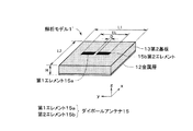
次に、本発明の第1実施例にかかる光伝導アンテナ1の解析モデルを図5および図6に示す。図5は光伝導アンテナ1の解析モデル1’の構成を示す斜視図であり、図6は光伝導アンテナ1の解析モデル1’の構成を示す側面図である。
本発明の第1実施例にかかる光伝導アンテナ1においては、テラヘルツ電磁波は金属層12で反射されて金属層12より下方へは放射されないため、第2基板13の上面に第1エレメント15aおよび第2エレメント15bが形成され、下面に金属層12が配置された図5,図6に示す構成を解析モデル1’の構成とすることができる。この図5,図6に示す解析モデル1’において、設計周波数fを500GHzとし、その自由空間の波長をλで表すとλは約0.6mmとなる。そして、解析モデル1’において設計した寸法を波長λを用いて表すと、第2基板13の長さL1と幅L2とは約1.41λとされ、第2基板13の高さHは約0.17λとされ、ダイポールアンテナ15の長さELの電気長は約0.5λとされ、第1エレメント15aと第2エレメント15bとが対向する給電点の間隔Dは約0.03λとされる。なお、第2基板13の比誘電率εr2は約3.0とされている。
Next, FIGS. 5 and 6 show analytical models of the
In the
この寸法条件により時間領域差分法シミュレータによりシミュレーションした解析モデル1’の入力インピーダンスの周波数特性を図7に、反射損失の周波数特性を図8に示す。300GHzから500GHzまで周波数をスキャンさせた際の入力インピーダンスが図7に示されており、図7を参照すると、入力インピーダンスの実部は周波数が300GHzの時に約20Ωとなり、周波数が高くなるにつれて次第に上昇していき、周波数が385GHzにおいて約49.6Ωとなり、周波数が500GHzにおいては約170Ωとなる。また、入力インピーダンスの虚部は周波数が300GHzの時に約−100Ωとなり、周波数が高くなるにつれて次第に上昇していき、周波数が385GHzにおいて約0Ωとなり、その後飽和して下降していき周波数が500GHzにおいては約51Ωとなる。また、300GHzから500GHzまで周波数をスキャンさせた際の反射損失が図8に示されており、図8を参照すると、反射損失は周波数が300GHzの時には約−1dBしか得られていないが、周波数が高くなるにつれて次第に減衰していき、周波数が385GHzにおいて共振して−30dB以下の良好な反射損失が得られている。そして、周波数が385GHzを超えていくと共振から外れて減衰量が少なくなっていき、周波数が500GHzにおいては約−5dBの減衰量となっている。
FIG. 7 shows the frequency characteristics of the input impedance and FIG. 8 shows the frequency characteristics of the reflection loss of the
上記した寸法では、約385GHzにおいて共振しており、この際に入力インピーダンスの虚部が約0Ωになると共に実部が約49.6Ωとなって、50Ωの特性インピーダンスに整合されるようになる。このように、約385GHzにおいて共振するのは第2基板13が誘電体とされて、その比誘電率εr2に基づいて波長が短縮されるからである。比誘電率εr2が3.0の場合は、波長短縮率は約71%になる。そこで、約385GHzにおいて共振している上記した寸法をスケーリングすることにより約500GHzに共振するように設計する。すなわち、解析モデル1’における各部の寸法を、385/500=0.77倍する。スケーリング後の解析モデル1’の寸法は、第2基板13の長さL1と幅L2とは約1.07λ(約0.64mm)とされ、第2基板13の高さHは約0.13λ(約0.078mm)とされ、ダイポールアンテナ15の長さELの電気長は約0.27λとされる。ただし、第1エレメント15aと第2エレメント15bとが対向する給電点の間隔Dは共振周波数に影響を与えないことからスケーリングされず約0.03λ(約0.018mm)とされる。
In the above dimensions, resonance occurs at about 385 GHz. At this time, the imaginary part of the input impedance becomes about 0Ω and the real part becomes about 49.6Ω, which is matched to the characteristic impedance of 50Ω. The reason why the resonance occurs at about 385 GHz is that the second substrate 13 is a dielectric and the wavelength is shortened based on the relative dielectric constant εr2. When the relative dielectric constant εr2 is 3.0, the wavelength shortening rate is about 71%. Therefore, the above-mentioned dimension that resonates at about 385 GHz is scaled so as to resonate at about 500 GHz. That is, the dimension of each part in the analysis model 1 'is multiplied by 385/500 = 0.77. The dimension of the
上記したようにスケーリングした寸法の解析モデル1’における入力インピーダンスの周波数特性を図9に、反射損失の周波数特性を図10に示す。400GHzから600GHzまで周波数をスキャンさせた際の入力インピーダンスが図9に示されており、図9を参照すると、入力インピーダンスの実部は周波数が400GHzの時に約20Ωとなり、周波数が高くなるにつれて次第に上昇していき、周波数が500GHzにおいて約47.3Ωとなり、周波数が600GHzにおいては約123Ωとなる。また、入力インピーダンスの虚部は周波数が400GHzの時に約−85Ωとなり、周波数が高くなるにつれて次第に上昇していき、周波数が500GHzにおいて約0Ωとなり、その後飽和するよう上昇していき周波数が600GHzにおいては約62Ωとなる。 FIG. 9 shows the frequency characteristics of the input impedance and FIG. 10 shows the frequency characteristics of the reflection loss in the analysis model 1 'having the scaled dimensions as described above. The input impedance when the frequency is scanned from 400 GHz to 600 GHz is shown in FIG. 9. Referring to FIG. 9, the real part of the input impedance is about 20Ω when the frequency is 400 GHz, and gradually increases as the frequency increases. Thus, the frequency is about 47.3Ω at 500 GHz, and about 123Ω at the frequency of 600 GHz. In addition, the imaginary part of the input impedance is about −85Ω when the frequency is 400 GHz, and gradually increases as the frequency becomes higher, becomes about 0Ω at the frequency of 500 GHz, and then increases so as to be saturated at the frequency of 600 GHz. About 62Ω.
また、400GHzから600GHzまで周波数をスキャンさせた際の反射損失が図10に示されており、図10を参照すると、反射損失は周波数が400GHzの時には約−1dBしか得られていないが、周波数が高くなるにつれて次第に減衰していき、周波数が500GHzにおいて共振して−20dB以下の良好な反射損失が得られている。そして、周波数が500GHzを超えていくと共振から外れて減衰量が少なくなっていき、周波数が600GHzにおいては約−6dBの減衰量となる。
このようにスケーリングすることにより、解析モデル1’を500GHzで共振するよう設計することができる。このことから、スケーリングをすることにより、400GHzや600GHzなどの周波数に共振するよう設計することができるようになる。
In addition, the reflection loss when the frequency is scanned from 400 GHz to 600 GHz is shown in FIG. 10. Referring to FIG. 10, the reflection loss is only about −1 dB when the frequency is 400 GHz. It gradually attenuates as the frequency increases, and a good reflection loss of -20 dB or less is obtained by resonating at a frequency of 500 GHz. When the frequency exceeds 500 GHz, the resonance is removed from the resonance, and the attenuation is reduced. When the frequency is 600 GHz, the attenuation is about −6 dB.
By scaling in this way, the
次に、図5,図6に示す解析モデル1’におけるy−z面の放射特性を図11に示し、x−z面の放射特性を図12に示す。この場合、解析モデル1’の寸法は上記したように500GHzにスケーリングした寸法とされ、周波数は約500GHzとされている。
図11を参照すると、解析モデル1’の放射方向とされるy−z面の0°方向(z軸方向)にC点で示す約5.8dBiの高い放射利得のビームが放射されている。また、解析モデル1’の下面方向には非常に小さいサイドローブしか放射されていないことが分かる。また、図12を参照すると解析モデル1’の放射方向とされるx−z面の0°方向(z軸方向)にC点で示す約5.8dBiの高い放射利得のビームが放射されている。また、解析モデル1’の下面方向にはわずかしか放射されていないことが分かる。また、周波数を490GHzにした場合は、解析モデル1’におけるy−z面およびx−z面の放射特性はほぼ同様となり、0°方向(z軸方向)の放射利得として若干増加した約5.9dBiが得られ、反射損失としては約−19.3dBが得られる。さらに、周波数を510GHzとした場合は、解析モデル1’におけるy−z面およびx−z面の放射特性はほぼ同様となり、0°方向(z軸方向)の放射利得として若干低下した約5.7dBiが得られ、反射損失としては約−20.8dBが得られる。
Next, the radiation characteristic of the yz plane in the
Referring to FIG. 11, a beam having a high radiation gain of about 5.8 dBi indicated by a point C is emitted in the 0 ° direction (z-axis direction) of the yz plane, which is the radiation direction of the
次に、解析モデル1’において第2基板13の高さHをパラメータとした際の入力インピーダンス特性を図13に示す。
第2基板13の高さHを0.1λから0.2λまで変化した際の入力インピーダンスの実部と虚部の変化が図13に示されている。図13を参照すると、入力インピーダンスの実部は高さHが0.1λの時に約30Ωとなり、高さHが0.125λ、0.15λと高くなるにつれて次第に上昇していく。そして、高さHが0.15λを超えると緩やかに上昇していき、高さHが0.2λとなると約68Ωになる。また、入力インピーダンスの虚部は高さHが0.1λの時に約0Ωとなり、高さHが0.125λを超えるまではほぼ0オームとなる。高さHが0.125λを超えていくと次第に虚部の絶対値が大きくなっていき、高さHが0.2λになると約−35Ωとなる。図13を参照すると、高さHを約0.13λとすることにより、50Ωの特性インピーダンスに整合することのできる入力インピーダンスが得られることが分かる。
Next, FIG. 13 shows input impedance characteristics when the height H of the second substrate 13 is used as a parameter in the
FIG. 13 shows changes in the real part and the imaginary part of the input impedance when the height H of the second substrate 13 is changed from 0.1λ to 0.2λ. Referring to FIG. 13, the real part of the input impedance is about 30Ω when the height H is 0.1λ, and gradually increases as the height H increases to 0.125λ and 0.15λ. And when the height H exceeds 0.15λ, it gradually rises, and when the height H becomes 0.2λ, it becomes about 68Ω. The imaginary part of the input impedance is about 0Ω when the height H is 0.1λ, and is almost 0 ohms until the height H exceeds 0.125λ. When the height H exceeds 0.125λ, the absolute value of the imaginary part gradually increases, and when the height H becomes 0.2λ, it becomes about −35Ω. Referring to FIG. 13, it can be seen that an input impedance that can be matched to a characteristic impedance of 50Ω can be obtained by setting the height H to about 0.13λ.
このように、解析モデル1’において、高い放射利得が得られるのは、図17に示す従来の光伝導アンテナ100のようにテラヘルツ電磁波が比誘電率が高く損失の多い光伝導膜110を透過することなく直接自由空間に放射される構成とされると共に、比誘電率εr2が約3と低く損失の少ない第2基板13を透過して金属層12で反射された反射波が、直接波にほぼ同相で合成されるからと考えられる。そして、上述した解析モデル1’に基づいて、図1,図2に示す第1実施例の光伝導アンテナ1が具現化されており、光伝導アンテナ1の各部の寸法は解析モデル1’における各部の寸法と同様とされている。
なお、上記説明した図7ないし図13の特性は、第2基板13の誘電体損(tanδ)がないものとした時の特性である。
Thus, in the
7 to 13 described above are characteristics when the second substrate 13 has no dielectric loss (tan δ).
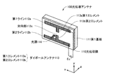
次に、本発明のテラヘルツ電磁波発生装置の第2実施例にかかる光伝導アンテナの構成を一部破断して示す斜視図を図14に示す。
図14に示す第2実施例の光伝導アンテナ2は、絶縁性あるいは半絶縁性の所定厚みの第1基板21の一面に光伝導層20が形成され、第1基板21の他面に金属層22が蒸着等により形成されている。第1基板21は、例えばGaAs基板とされ、光伝導層20の材料は、例えば低温成長GaAs(比誘電率εr1は約13)とされ、金属層22の材料は金、銀、アルミニウムや銅等とされる。金属層22の上面には所定厚みの絶縁性の第2基板23が貼着されている。第2基板23の材料は、例えばフッ素樹脂(比誘電率εr2は約3)とされる。この第2基板23の上面に、第1エレメント25a1および第2エレメント25b1からなる第1ダイポールアンテナ25−1と、第1エレメント25a2および第2エレメント25b2からなる第2ダイポールアンテナ25−2と、第1エレメント25a3および第2エレメント25b3からなる第3ダイポールアンテナ25−3の3つのダイポールアンテナが蒸着等により形成されている。
Next, FIG. 14 is a perspective view showing a partially broken structure of the photoconductive antenna according to the second embodiment of the terahertz electromagnetic wave generator of the present invention.
In the photoconductive antenna 2 of the second embodiment shown in FIG. 14, a
3つの第1エレメント25a1〜25a3と3つの第2エレメント25b1〜25b3とが対向する第1ダイポールアンテナ25−1〜第3ダイポールアンテナ25−3の給電点から、3本の第1ライン26a1,26a2,26a3および3本の第2ライン26b1,26b2,26b3がそれぞれ内部に向かってほぼ平行に引き出されている。第1ライン26a1〜26a3および第2ライン26b1〜26b3は、第2基板23、金属層22、第1基板21および光伝導層20を貫通して、光伝導層20の外表面上に引き出されており、光伝導層20の外表面上に沿って第1共通ライン26dおよび第2共通ライン26eが形成されている。そして、第1ライン26a1〜26a3および第2ライン26b1〜26b3がそれぞれ第1共通ライン26dおよび第2共通ライン26eに接続されている。光伝導層20上に形成されている第2共通ライン26eには切欠部26cが形成されている。この場合、金属層22と第1ライン26a1〜26a3および第2ライン26b1〜26b3とが短絡しないように、金属層22には第1ライン26a1〜26a3および第2ライン26b1〜26b3の外形寸法より大きな寸法の孔部が形成される。また、切欠部26cの間隔は、例えば数μm程度とされると共に、第1共通ライン26dおよび第2共通ライン26eとでコプレーナラインを形成することができる。第1ダイポールアンテナ25−1〜第3ダイポールアンテナ25−3が形成されている第2基板23の上面には、レンズ24が貼着されている。
From the feeding point of the first dipole antenna 25-1 to the third dipole antenna 25-3 where the three first elements 25a1 to 25a3 and the three second elements 25b1 to 25b3 face each other, the three first lines 26a1 and 26a2 are provided. , 26a3 and three second lines 26b1, 26b2, 26b3 are drawn out substantially in parallel toward the inside. The first lines 26 a 1 to 26 a 3 and the second lines 26
このような構成の第2実施例の光伝導アンテナ2において、第1共通ライン26dおよび第2共通ライン26eの端部との間に直流のバイアス電圧Ecを印加する。この状態では、第2共通ライン26eは切欠部26cにより絶縁されており、第1共通ライン26dおよび第2共通ライン26eに電流は流れない。ここで、光源27から10-15秒程度のフェムト秒パルスレーザ光を第2共通ライン26eにおける切欠部26cに照射する。パルスレーザ光を切欠部26cに照射すると、切欠部26cにおける光伝導層20中に光導電効果により自由キャリアが生じ、この自由キャリアがバイアス電圧Ecにより加速されることにより、切欠部26cにサブピコ秒(10-12秒)程度のパルス状の電流が流れる。このパルス状の電流は第1共通ライン26dおよび第2共通ライン26eと、第1ライン26a1〜26a3および第2ライン26b1〜26b3とを介して第1ダイポールアンテナ25−1〜第3ダイポールアンテナ25−3に同相に供給されて、テラヘルツ電磁波が第1ダイポールアンテナ25−1〜第3ダイポールアンテナ25−3からそれぞれ放射される。なお、第1ダイポールアンテナ25−1、第2ダイポールアンテナ25−2、第3ダイポールアンテナ25−3に同相で給電されるように、給電線路の長さの違いはnλとされている。ただし、nは整数、λは使用する周波数の波長である。これにより、第1ダイポールアンテナ25−1ないし第3ダイポールアンテナ25−3から放射されるテラヘルツ電磁波の位相が同相となる。
In the photoconductive antenna 2 of the second embodiment having such a configuration, a DC bias voltage Ec is applied between the end portions of the first common line 26d and the second common line 26e. In this state, the second common line 26e is insulated by the notch 26c, and no current flows through the first common line 26d and the second common line 26e. Here, a femtosecond pulse laser beam of about 10 −15 seconds is irradiated from the light source 27 to the cutout portion 26c in the second common line 26e. When the pulse laser beam is irradiated to the notch 26c, free carriers are generated in the
このように、切欠部26cが3組の第1ダイポールアンテナ25−1〜第3ダイポールアンテナ25−3の給電部となる。この場合、第2基板23の下面に配置された金属層22の作用により、第1ダイポールアンテナ25−1〜第3ダイポールアンテナ25−3から放射されたテラヘルツ電磁波が反射され、この反射波がz軸方向に同相で放射されたテラヘルツ電磁波とほぼ同相で合成されることによりz軸方向へ強く放射される。合成されたテラヘルツ電磁波は、レンズ24により収束されるようになる。この場合、光伝導アンテナ4は3つのダイポールアンテナ25−1〜25−3から同相でテラヘルツ電磁波が放射されるアレーアンテナとされていることから、z軸方向により強く電磁波が放射される。なお、第1ダイポールアンテナ25−1〜第3ダイポールアンテナ25−3の電気長は、放射されるテラヘルツ電磁波の波長をλとした際に約λ/2の長さとされる。また、第2基板23の厚さは、放射されるテラヘルツ電磁波の波長をλとした際に約λ/4の電気長が得られる厚さとされるのが好適である。さらに、レンズ24は、例えばシリコンレンズとされ、レンズ24の上部形状が凸状の膨出部を備える形状とされて、テラヘルツ電磁波を収束している。なお、レンズ24を省略しても良い。 As described above, the notch portion 26c serves as a feeding portion for the three sets of the first dipole antenna 25-1 to the third dipole antenna 25-3. In this case, the terahertz electromagnetic wave radiated from the first dipole antenna 25-1 to the third dipole antenna 25-3 is reflected by the action of the metal layer 22 disposed on the lower surface of the second substrate 23, and this reflected wave is z The terahertz electromagnetic wave radiated in the same phase in the axial direction is synthesized in substantially the same phase as the terahertz electromagnetic wave, so that it is strongly radiated in the z-axis direction. The synthesized terahertz electromagnetic wave is converged by the lens 24. In this case, since the photoconductive antenna 4 is an array antenna that emits terahertz electromagnetic waves in phase from the three dipole antennas 25-1 to 25-3, electromagnetic waves are radiated more strongly in the z-axis direction. The electrical length of the first dipole antenna 25-1 to the third dipole antenna 25-3 is approximately λ / 2 when the wavelength of the radiated terahertz electromagnetic wave is λ. Further, the thickness of the second substrate 23 is preferably set to a thickness that provides an electrical length of about λ / 4 when the wavelength of the radiated terahertz electromagnetic wave is λ. Further, the lens 24 is, for example, a silicon lens, and the upper shape of the lens 24 is a shape having a convex bulge, and converges terahertz electromagnetic waves. The lens 24 may be omitted.
第2実施例の光伝導アンテナ2は、3組の第1ダイポールアンテナ25−1〜第3ダイポールアンテナ25−3からなるアレーアンテナを備え、z軸方向へ同相で放射されることからビームが鋭くなり放射利得を第1実施例の光伝導アンテナ1より向上することができる。なお、本発明の第2実施例の光伝導アンテナ2においても、テラヘルツ電磁波が比誘電率が高く損失の多い光伝導膜を透過することなく直接自由空間に放射される構成とされると共に、比誘電率εr2が約3と低く損失の少ない第2基板23を透過して金属層22で反射された反射波が、直接波にほぼ同相で合成されることから、高い放射利得を得ることができる。
The photoconductive antenna 2 of the second embodiment includes an array antenna composed of three sets of first dipole antenna 25-1 to third dipole antenna 25-3, and is radiated in the same phase in the z-axis direction, so that the beam is sharp. Therefore, the radiation gain can be improved as compared with the
次に、本発明のテラヘルツ電磁波発生装置の第3実施例にかかる光伝導アンテナの構成を示す斜視図を図15に示す。
図15に示す第3実施例の光伝導アンテナ3は、金属板33の上に絶縁性あるいは半絶縁性の所定厚みの第1基板31と、所定厚みの絶縁性の第2基板32とが横方向に密着するよう接着されて一体になるよう配置されている。第1基板31の表面には光伝導層30が形成されている。第1基板31は、例えばGaAs基板とされ、光伝導層30の材料は、例えば低温成長GaAs(比誘電率εr1は約13)とされ、第2基板32の材料は、例えばフッ素樹脂(比誘電率εr2は約3)とされ金属板33の材料は金、銀、アルミニウムや銅等とされる。この第2基板32の表面に、第1エレメント34aおよび第2エレメント34bからなるダイポールアンテナ34が蒸着等により形成されている。第1エレメント34aと第2エレメント34bとが対向するダイポールアンテナ34の給電点から、第1ライン35aおよび第2ライン35bがほぼ平行に第2基板32の表面に形成されている。
Next, FIG. 15 is a perspective view showing the configuration of the photoconductive antenna according to the third embodiment of the terahertz electromagnetic wave generator of the present invention.
In the photoconductive antenna 3 of the third embodiment shown in FIG. 15, a first substrate 31 having a predetermined thickness of insulating or semi-insulating and a second substrate 32 of insulating having a predetermined thickness are placed on a metal plate 33. It is arranged so as to be bonded and united so as to be in close contact with the direction. A
この第1ライン35aおよび第2ライン35bは第1基板31側へ延伸されて、第1基板31の表面の光伝導層30上にも形成されている。光伝導層30上に形成されている第1ライン35aの中途は切断されてL字状に折曲されて外部へ引き出されるように形成されている。また、第1ライン35aおよび第2ライン35bの先端部は対向部35cを介して対向するように形成されている。この場合、対向部35cの間隔は、例えば数μm程度とされると共に、第1ライン35aおよび第2ライン35bは金属板33がグランドプレーンとされてマイクロストリップラインを形成することができる。また、ダイポールアンテナ34が形成されている第2基板32の上面にレンズを設けるようにしてもよい。
このような構成の第3実施例の光伝導アンテナ3において、第1ライン35aの中途に形成されたL字状に折曲された端部間に直流のバイアス電圧Ecを印加する。この状態では、第1ライン35aおよび第2ライン35bの間は対向部35cにより絶縁されて電流は流れず、第1エレメント34aおよび第2エレメント34bからなるダイポールアンテナ34からの放射はない。
The first line 35 a and the second line 35 b are extended to the first substrate 31 side and are also formed on the
In the photoconductive antenna 3 of the third embodiment having such a configuration, a DC bias voltage Ec is applied between the end portions bent in an L shape formed in the middle of the first line 35a. In this state, the first line 35a and the second line 35b are insulated by the facing portion 35c and no current flows, and there is no radiation from the dipole antenna 34 including the first element 34a and the second element 34b.
ここで、光源36から10-15秒程度のフェムト秒パルスレーザ光を第1ライン35aにおける対向部35cに照射する。パルスレーザ光が対向部35cに照射されると、対向部35cにおける光伝導層30中に光導電効果により自由キャリアが生じ、この自由キャリアがバイアス電圧Ecにより加速されることにより、対向部35cにサブピコ秒(10-12秒)程度のパルス状の電流が流れる。このパルス状の電流により、第1ライン35aおよび第2ライン35bを介してダイポールアンテナ34が励振されて、テラヘルツ電磁波が第1エレメント34aおよび第2エレメント34bからなるダイポールアンテナ34から放射される。このように、対向部35cがダイポールアンテナ34の給電部となる。この場合、第2基板32の下面に配置された金属板33の作用により、ダイポールアンテナ34から下方へ放射されたテラヘルツ電磁波が反射され、この反射波はz軸方向に放射されたテラヘルツ電磁波とほぼ同相で合成されることによりz軸方向に強く放射される。なお、ダイポールアンテナ34の電気長は、放射されるテラヘルツ電磁波の波長をλとした際に約λ/2の長さとされる。また、第2基板32の厚さは、放射されるテラヘルツ電磁波の波長をλとした際に約λ/4の電気長が得られる厚さとされるのが好適とされる。また、第2基板32の上面にレンズを設けると、テラヘルツ電磁波を収束することができる。
第3実施例の光伝導アンテナ3は、テラヘルツ電磁波が比誘電率が高く損失の多い光伝導膜を透過することなく直接自由空間に放射される構成とされると共に、比誘電率εr2が約3と低く損失の少ない第2基板32を透過して金属板33で反射された反射波が、直接波にほぼ同相で合成されることから、高い放射利得を得ることができる。
Here, the facing portion 35c in the first line 35a is irradiated with femtosecond pulsed laser light of about 10 −15 seconds from the light source. When the facing portion 35c is irradiated with the pulse laser beam, free carriers are generated in the
The photoconductive antenna 3 of the third embodiment is configured such that terahertz electromagnetic waves are directly radiated to free space without passing through a photoconductive film having a high relative dielectric constant and a large loss, and a relative dielectric constant εr2 of about 3 Since the reflected wave that has been transmitted through the second substrate 32 with low loss and reflected by the metal plate 33 is combined with the direct wave in almost the same phase, a high radiation gain can be obtained.
次に、本発明のテラヘルツ電磁波発生装置の第4実施例にかかる光伝導アンテナの構成を示す斜視図を図16に示す。
図16に示す第4実施例の光伝導アンテナ4は、金属板43の上に絶縁性あるいは半絶縁性の所定厚みの第1基板41と、所定厚みの絶縁性の第2基板42とが横方向に密着するよう接着されて一体になるよう配置されている。第1基板41の表面には光伝導層40が形成されている。第1基板41は、例えばGaAs基板とされ、光伝導層40の材料は、例えば低温成長GaAs(比誘電率εr1は約13)とされ、第2基板42の材料は、例えばフッ素樹脂(比誘電率εr2は約3)とされ金属板43の材料は金、銀、アルミニウムや銅等とされる。この第2基板42の表面に、第1エレメント44a1および第2エレメント44b1からなる第1ダイポールアンテナ44−1と、第1エレメント44a2および第2エレメント44b2からなる第2ダイポールアンテナ44−2と、第1エレメント44a3および第2エレメント44b3からなる第3ダイポールアンテナ44−3の3つのダイポールアンテナが蒸着等により形成されている。
Next, FIG. 16 is a perspective view showing the configuration of the photoconductive antenna according to the fourth embodiment of the terahertz electromagnetic wave generator of the present invention.
In the photoconductive antenna 4 of the fourth embodiment shown in FIG. 16, a first substrate 41 having a predetermined thickness, which is insulative or semi-insulating, and a second substrate 42 having a predetermined thickness are horizontally disposed on a metal plate 43. It is arranged so as to be bonded and united so as to be in close contact with the direction. A
第2基板42の表面に第1ライン45aおよび第2ライン45bがほぼ平行に形成されており、3つの第1エレメント44a1〜44a3の給電点が第1ライン45aにそれぞれ接続されており、3つの第2エレメント44b1〜44b3の給電点が第2ライン45bにそれぞれ接続されている。この場合、第1ライン45aおよび第2ライン45bに接続される第1ダイポールアンテナ44−1ないし第3ダイポールアンテナ44−3の給電点の間の電気長は約nλとされている。ただし、nは整数、λは使用する周波数の波長である。これにより、第1ダイポールアンテナ44−1ないし第3ダイポールアンテナ44−3から放射されるテラヘルツ電磁波の位相が同相となる。
第1ライン45aおよび第2ライン45bは第1基板41側へ延伸されて、第1基板41の表面の光伝導層40上にも形成されている。光伝導層40上に形成されている第1ライン45aの中途は切断されてL字状に折曲されて外部へ引き出されるように形成されている。また、第1ライン45aおよび第2ライン45bの先端部は対向部45cを介して対向するように形成されている。この場合、対向部45cの間隔は、例えば数μm程度とされると共に、第1ライン45aおよび第2ライン45bは金属板43がグランドプレーンとされてマイクロストリップラインを形成することができる。また、3つのダイポールアンテナ44−1〜44−3が形成されている第2基板42の上面にレンズを設けるようにしてもよい。
The first line 45a and the second line 45b are formed substantially in parallel on the surface of the second substrate 42. The feeding points of the three first elements 44a1 to 44a3 are connected to the first line 45a, respectively. The feeding points of the second elements 44b1 to 44b3 are connected to the second line 45b, respectively. In this case, the electrical length between the feeding points of the first dipole antenna 44-1 to the third dipole antenna 44-3 connected to the first line 45a and the second line 45b is about nλ. Here, n is an integer and λ is the wavelength of the frequency to be used. Thereby, the phase of the terahertz electromagnetic wave radiated from the first dipole antenna 44-1 to the third dipole antenna 44-3 is in phase.
The first line 45 a and the second line 45 b are extended to the first substrate 41 side and are also formed on the
このような構成の第4実施例の光伝導アンテナ4において、第1ライン45aの中途に形成されたL字状に折曲された端部間に直流のバイアス電圧Ecを印加する。この状態では、第1ライン45aおよび第2ライン45bの間は対向部45cにより絶縁されて電流は流れず、第1エレメント44a1〜44a3および第2エレメント44b1〜44b3からなる3つのダイポールアンテナ44−1〜44−3からの放射はない。ここで、光源46から10-15秒程度のフェムト秒パルスレーザ光を第1ライン45aと第2ライン45bとの間に形成された対向部45cに照射する。パルスレーザ光が対向部45cに照射されると、対向部45cにおける光伝導層40中に光導電効果により自由キャリアが生じ、この自由キャリアがバイアス電圧Ecにより加速されることにより、対向部45cにサブピコ秒(10-12秒)程度のパルス状の電流が流れる。このパルス状の電流により、第1ライン45aおよび第2ライン45bを介して3つのダイポールアンテナ44−1〜44−3が励振されて、テラヘルツ電磁波が第1エレメント44a1〜44a3および第2エレメント44b1〜44b3からなる3つのダイポールアンテナ44−1〜44−3から放射される。このように、対向部45cが3つのダイポールアンテナ44−1〜44−3の給電部となる。
In the photoconductive antenna 4 of the fourth embodiment having such a configuration, a DC bias voltage Ec is applied between the end portions bent in an L shape formed in the middle of the first line 45a. In this state, the first line 45a and the second line 45b are insulated by the facing portion 45c and no current flows, and the three dipole antennas 44-1 including the first elements 44a1 to 44a3 and the second elements 44b1 to 44b3. There is no radiation from ~ 44-3. Here, a femtosecond pulsed laser beam of about 10 −15 seconds is emitted from the light source 46 to the facing portion 45c formed between the first line 45a and the second line 45b. When the facing portion 45c is irradiated with the pulse laser beam, free carriers are generated in the
この場合、第2基板42の下面に配置された金属板43の作用により、3つのダイポールアンテナ44−1〜44−3から下方へ放射されたテラヘルツ電磁波が反射され、この反射波はz軸方向に同相で放射されたテラヘルツ電磁波とほぼ同相で合成されることによりz軸方向に強く放射される。この場合、光伝導アンテナ4は3つのダイポールアンテナ44−1〜44−3から同相でテラヘルツ電磁波が放射されるアレーアンテナとされていることから、z軸方向により強く電磁波が放射される。なお、ダイポールアンテナ44−1〜44−3の電気長は、放射されるテラヘルツ電磁波の波長をλとした際に約λ/2の長さとされる。また、第2基板42の厚さは、放射されるテラヘルツ電磁波の波長をλとした際に約λ/4の電気長が得られる厚さとされるのが好適とされる。また、第2基板42の上面にレンズを設けると、テラヘルツ電磁波を収束することができる。
第4実施例の光伝導アンテナ4は、テラヘルツ電磁波が比誘電率が高く損失の多い光伝導膜を透過することなく直接自由空間に放射される構成とされると共に、比誘電率εr2が約3と低く損失の少ない第2基板42を透過して金属板43で反射された反射波が、直接波にほぼ同相で合成されると共にアレーアンテナとされていることから、高い放射利得を得ることができる。
In this case, terahertz electromagnetic waves radiated downward from the three dipole antennas 44-1 to 44-3 are reflected by the action of the metal plate 43 disposed on the lower surface of the second substrate 42, and this reflected wave is reflected in the z-axis direction. Are strongly radiated in the z-axis direction by being synthesized almost in phase with the terahertz electromagnetic wave radiated in phase. In this case, since the photoconductive antenna 4 is an array antenna that emits terahertz electromagnetic waves in phase from the three dipole antennas 44-1 to 44-3, electromagnetic waves are radiated more strongly in the z-axis direction. The electrical length of the dipole antennas 44-1 to 44-3 is approximately λ / 2 when the wavelength of the radiated terahertz electromagnetic wave is λ. The thickness of the second substrate 42 is preferably set to a thickness that provides an electrical length of about λ / 4 when the wavelength of the radiated terahertz electromagnetic wave is λ. In addition, when a lens is provided on the upper surface of the second substrate 42, terahertz electromagnetic waves can be converged.
The photoconductive antenna 4 of the fourth embodiment is configured such that terahertz electromagnetic waves are directly radiated to free space without passing through a photoconductive film having a high relative permittivity and a large loss, and a relative permittivity εr2 of about 3 Since the reflected wave that has been transmitted through the second substrate 42 with low loss and reflected by the metal plate 43 is combined with the direct wave in substantially the same phase and is used as an array antenna, a high radiation gain can be obtained. it can.
以上説明した本発明の光伝導アンテナにおいて、光伝導層の材料は低温成長GaAsに限らず、イオン注入InP(Indium Phosphide)、イオン注入シリコン、MOCVD(Metal Organic Chemical Vapor Deposition )CdTe( Cadmium Telluride)、イオン注入ゲルマニウム等のキャリア寿命が短く、移動度が大きい材料を用いることができる。また、上記した光伝導アンテナの寸法は一例であって、この寸法に限ることはない。
ここで、本発明の第1実施例の光伝導アンテナ1の製造方法の概略を説明すると、GaAsの第1基板11の一面にGaAsを低温成長させることにより光伝導層10を作成する。次いで、第1基板11の他面に金属層12を蒸着等により形成する。フッ素樹脂からなる第2基板13の上面に金属層を蒸着等により形成し、次いで、金属層をエッチングすることにより第1エレメント15aおよび第2エレメント15bからなるダイポールアンテナ15を形成する。光伝導層10の上面に金属層を蒸着等により形成して、金属層をエッチングすることにより第1ライン16aと、切欠部16cを備える第2ライン16bとを形成する。ここで、第1基板11の金属層12の上面に第2基板13の下面を貼着することにより、第1基板11上に第2基板13を一体化する。そして、ダイポールアンテナ15の給電点の位置からエッチングすることにより、第2基板13と金属層12と第1基板11と光伝導層10までスルーホールを形成する。次いで、スルーホール内を金属メッキしてスルーホールと第1ライン16aおよび第2ライン16bとに電気的に接続する。これにより、第1実施例の光伝導アンテナ1を製造することができる。
In the photoconductive antenna of the present invention described above, the material of the photoconductive layer is not limited to low-temperature grown GaAs, but ion-implanted InP (Indium Phosphide), ion-implanted silicon, MOCVD (Metal Organic Chemical Vapor Deposition) CdTe (Cadmium Telluride), A material having a short carrier life and high mobility, such as ion-implanted germanium, can be used. Moreover, the dimension of the above-mentioned photoconductive antenna is an example, and is not limited to this dimension.
Here, the outline of the manufacturing method of the
また、本発明の第2実施例の光伝導アンテナ2は、第1実施例の光伝導アンテナ1とほぼ同様の製造方法により製造することができる。さらに、本発明の第3実施例の光伝導アンテナ3は、第1基板31の表面にGaAsを低温成長させることにより光伝導層30を形成する。次いで、金属板33の上にGaAsの第1基板31と、フッ素樹脂からなる第2基板32とを横方向に密着させて接着する。第1基板31と第2基板32とは一側辺同士が接着される。そして、第1基板31および第2基板32の表面の全面に金属層を蒸着等により形成し、次いで、金属層をエッチングすることにより第1エレメント34aおよび第2エレメント34bからなるダイポールアンテナ34と、第1ライン35aおよび第2ライン35bを形成する。この際に、対向部35cも形成される。これにより、第3実施例の光伝導アンテナ3を製造することができる。本発明の第4実施例の光伝導アンテナ4は、第3実施例の光伝導アンテナ3とほぼ同様の製造方法により製造することができる。
Further, the photoconductive antenna 2 of the second embodiment of the present invention can be manufactured by a manufacturing method almost the same as the
1 光伝導アンテナ、2 光伝導アンテナ、3 光伝導アンテナ、10 光伝導層、11 第1基板、12 金属層、13 第2基板、14 レンズ、14a 膨出部、15 ダイポールアンテナ、15a 第1エレメント、15b 第2エレメント、16a 第1ライン、16b 第2ライン、16c 切欠部、17 光源、20 光伝導層、21 第1基板、22 金属層、23 第2基板、24 レンズ、25 ダイポールアンテナ、25−1 第1ダイポールアンテナ、25−2 第2ダイポールアンテナ、25−3 第3ダイポールアンテナ、25a1,25a2,25a3 第1エレメント、25b1,25b2,25b3 第2エレメント、26a1,26a2,26a3 第1ライン、26b1,26b2,26b3 第2ライン、26c 切欠部、26d 第1共通ライン、26e 第2共通ライン、27 光源、30 光伝導層、31 第1基板、32 第2基板、33 金属板、34 ダイポールアンテナ、34a 第1エレメント、34b 第2エレメント、35a 第1ライン、35b 第2ライン、35c 対向部、36 光源、44−1 第1ダイポールアンテナ、44−2 第2ダイポールアンテナ、44−3 第3ダイポールアンテナ、44a1,44a2,44a3 第1エレメント、44b1,44b2,44b3 第2エレメント、45a 第1ライン、45b 第2ライン、45c 対向部、46 光源、100 光伝導アンテナ、110 光伝導膜、111 第1基板、112a 第1ライン、112b 第2ライン、112c 対向部、113 ダイポールアンテナ、113a 第1エレメント、113b 第2エレメント、114 光源 DESCRIPTION OF SYMBOLS 1 Photoconductive antenna, 2 Photoconductive antenna, 3 Photoconductive antenna, 10 Photoconductive layer, 11 1st board | substrate, 12 Metal layer, 13 2nd board | substrate, 14 Lens, 14a Bumping part, 15 Dipole antenna, 15a 1st element 15b Second element, 16a First line, 16b Second line, 16c Notch, 17 Light source, 20 Photoconductive layer, 21 First substrate, 22 Metal layer, 23 Second substrate, 24 Lens, 25 Dipole antenna, 25 -1 first dipole antenna, 25-2 second dipole antenna, 25-3 third dipole antenna, 25a1, 25a2, 25a3 first element, 25b1, 25b2, 25b3 second element, 26a1, 26a2, 26a3 first line, 26b1, 26b2, 26b3 Second line, 26c Notch , 26d first common line, 26e second common line, 27 light source, 30 photoconductive layer, 31 first substrate, 32 second substrate, 33 metal plate, 34 dipole antenna, 34a first element, 34b second element, 35a First line, 35b Second line, 35c Opposing part, 36 Light source, 44-1 First dipole antenna, 44-2 Second dipole antenna, 44-3 Third dipole antenna, 44a1, 44a2, 44a3 First element, 44b1 44b2, 44b3 second element, 45a first line, 45b second line, 45c facing part, 46 light source, 100 photoconductive antenna, 110 photoconductive film, 111 first substrate, 112a first line, 112b second line, 112c Opposing part, 113 Dipole antenna, 113 The first element, 113b second element, 114 a light source
Claims (5)
該金属板上に配置され、光が照射された際に自由電子が生じる比誘電率εr1の光伝導層が表面に形成された絶縁性の第1基板と、
前記金属板上に前記第1基板の横に隣接して密着するよう配置された比誘電率εr2の絶縁性の第2基板と、
該第2基板の表面に形成された導電性のダイポールアンテナのエレメントと、
該ダイポールアンテナの給電点から引き出され、前記第2基板の表面から前記第1基板における前記光伝導層上にわたって形成された第1ラインおよび第2ラインと、
前記光伝導層上に形成されている前記第1ラインと前記第2ラインの端部が所定の間隔で対向している対向部と、
該対向部にパルス状の光を照射する光源と、
前記第1ラインと前記第2ラインとの間に電源を印加するバイアス電源とを備え、
比誘電率εr1>比誘電率εr2とされていることを特徴とするテラヘルツ電磁波発生装置。 A metal plate,
An insulating first substrate disposed on the metal plate and having a photoconductive layer having a relative dielectric constant εr1 that generates free electrons when irradiated with light;
An insulating second substrate having a relative dielectric constant εr2 disposed on the metal plate so as to be in close contact with the side of the first substrate;
An element of a conductive dipole antenna formed on the surface of the second substrate;
A first line and a second line drawn from a feeding point of the dipole antenna and formed from the surface of the second substrate to the photoconductive layer of the first substrate;
An opposing portion in which end portions of the first line and the second line formed on the photoconductive layer oppose each other at a predetermined interval;
A light source that emits pulsed light to the facing portion;
A bias power source for applying a power source between the first line and the second line;
A terahertz electromagnetic wave generator characterized in that the relative permittivity εr1> relative permittivity εr2.
前記金属層上に配置された比誘電率εr2の絶縁性の第2基板と、
該第2基板の表面に形成された導電性のダイポールアンテナのエレメントと、
該ダイポールアンテナの給電点から引き出され、前記第2の基板、前記金属層、前記第1の基板および前記光伝導層を貫通して、前記光伝導層上に形成された第1ラインおよび第2ラインと、
前記光伝導層上に形成されている前記第2ラインに形成された切欠部と、
該切欠部にパルス状の光を照射する光源と、
前記第1ラインの端部と、前記第2ラインの端部との間に印加されたバイアス電源とを備え、
比誘電率εr1>比誘電率εr2とされていることを特徴とするテラヘルツ電磁波発生装置。 An insulating first substrate having a relative permittivity εr1 in which a photoconductive layer that generates free electrons when irradiated with light is formed on one surface and a metal layer is formed on the other surface;
An insulating second substrate having a relative dielectric constant εr2 disposed on the metal layer;
An element of a conductive dipole antenna formed on the surface of the second substrate;
A first line and a second line that are drawn from the feeding point of the dipole antenna , penetrate the second substrate, the metal layer, the first substrate, and the photoconductive layer, and are formed on the photoconductive layer. Line,
A notch formed in the second line formed on the photoconductive layer;
A light source for irradiating the notch with pulsed light;
A bias power source applied between an end of the first line and an end of the second line;
A terahertz electromagnetic wave generator characterized in that the relative permittivity εr1> relative permittivity εr2.
Priority Applications (1)
| Application Number | Priority Date | Filing Date | Title |
|---|---|---|---|
| JP2010098684A JP5517127B2 (en) | 2010-04-22 | 2010-04-22 | Terahertz electromagnetic wave generator |
Applications Claiming Priority (1)
| Application Number | Priority Date | Filing Date | Title |
|---|---|---|---|
| JP2010098684A JP5517127B2 (en) | 2010-04-22 | 2010-04-22 | Terahertz electromagnetic wave generator |
Publications (3)
| Publication Number | Publication Date |
|---|---|
| JP2011228572A JP2011228572A (en) | 2011-11-10 |
| JP2011228572A5 JP2011228572A5 (en) | 2013-05-09 |
| JP5517127B2 true JP5517127B2 (en) | 2014-06-11 |
Family
ID=45043576
Family Applications (1)
| Application Number | Title | Priority Date | Filing Date |
|---|---|---|---|
| JP2010098684A Active JP5517127B2 (en) | 2010-04-22 | 2010-04-22 | Terahertz electromagnetic wave generator |
Country Status (1)
| Country | Link |
|---|---|
| JP (1) | JP5517127B2 (en) |
Families Citing this family (2)
| Publication number | Priority date | Publication date | Assignee | Title |
|---|---|---|---|---|
| EP3035394A1 (en) | 2014-12-17 | 2016-06-22 | Centre National de la Recherche Scientifique | Photoconductive antenna for terahertz waves, method for producing such photoconductive antenna and terahertz time domain spectroscopy system |
| WO2022091992A1 (en) * | 2020-10-28 | 2022-05-05 | 国立大学法人大阪大学 | Terahertz light source, fluid detector, and terahertz wave generating method |
-
2010
- 2010-04-22 JP JP2010098684A patent/JP5517127B2/en active Active
Also Published As
| Publication number | Publication date |
|---|---|
| JP2011228572A (en) | 2011-11-10 |
Similar Documents
| Publication | Publication Date | Title |
|---|---|---|
| Nassar et al. | A novel method for improving antipodal Vivaldi antenna performance | |
| Chu et al. | Design of compact dual-wideband antenna with assembled monopoles | |
| Kan et al. | Simple broadband planar CPW-fed quasi-Yagi antenna | |
| CN105190991B (en) | Waveguide component | |
| Lu et al. | InP-based THz beam steering leaky-wave antenna | |
| Perruisseau-Carrier et al. | Graphene antennas: Can integration and reconfigurability compensate for the loss? | |
| JP4977048B2 (en) | Antenna element | |
| Nguyen et al. | Size and weight reduction of integrated lens antennas using a cylindrical air cavity | |
| US8957441B2 (en) | Integrated antenna device module for generating terahertz continuous wave and fabrication method thereof | |
| Dheyab et al. | Design and optimization of rectangular microstrip patch array antenna using frequency selective surfaces for 60 GHz | |
| JP5517127B2 (en) | Terahertz electromagnetic wave generator | |
| Montero-de-Paz et al. | Meander dipole antenna to increase CW THz photomixing emitted power | |
| WO2021070921A1 (en) | Terahertz device | |
| Ederra et al. | Design and test of a 0.5 THz dipole antenna with integrated Schottky diode detector on a high dielectric constant ceramic electromagnetic bandgap substrate | |
| Dhiflaoui et al. | Numerical analysis of wideband and high directive bowtie THz photoconductive antenna | |
| Kaur et al. | On the design defected ground plane based L slotted microstrip patch antenna for C band applications | |
| Yahyaoui et al. | Design and comparative analysis of ultra-wideband and high directive antennas for THz applications | |
| Deshmukh et al. | Broadband gap-coupled slot cut rectangular microstrip antennas | |
| Demshevsky et al. | Investigation of an UWB antipodal tapered slot antenna element based on substrate integrated waveguide in an antenna array | |
| KR102111143B1 (en) | Semiconductor on-chip antenna | |
| Shafee et al. | Stacked resonator patch antenna for wide bandwidth THz detection | |
| Alharbi et al. | Broadband bow-tie slot antenna with tuning stub for resonant tunnelling diode oscillators with novel configuration for substrate effects suppression | |
| Rafique et al. | A wideband slot-coupled inverted microstrip patch antenna for wireless communications | |
| Nguyen et al. | Air gap effect on antenna characteristics of slitline and stripline dipoles on an extended hemispherical lens substrate | |
| Lin et al. | An Ultra-wideband Elliptical Bowtie Antenna With Depressed Bias for THz Vacuum Photomixers |
Legal Events
| Date | Code | Title | Description |
|---|---|---|---|
| A521 | Written amendment |
Free format text: JAPANESE INTERMEDIATE CODE: A523 Effective date: 20130326 |
|
| A621 | Written request for application examination |
Free format text: JAPANESE INTERMEDIATE CODE: A621 Effective date: 20130326 |
|
| TRDD | Decision of grant or rejection written | ||
| A01 | Written decision to grant a patent or to grant a registration (utility model) |
Free format text: JAPANESE INTERMEDIATE CODE: A01 Effective date: 20140318 |
|
| A61 | First payment of annual fees (during grant procedure) |
Free format text: JAPANESE INTERMEDIATE CODE: A61 Effective date: 20140324 |
|
| R150 | Certificate of patent or registration of utility model |
Ref document number: 5517127 Country of ref document: JP Free format text: JAPANESE INTERMEDIATE CODE: R150 |
|
| R250 | Receipt of annual fees |
Free format text: JAPANESE INTERMEDIATE CODE: R250 |
|
| R250 | Receipt of annual fees |
Free format text: JAPANESE INTERMEDIATE CODE: R250 |
|
| R250 | Receipt of annual fees |
Free format text: JAPANESE INTERMEDIATE CODE: R250 |