JP5490317B2 - Method and apparatus for controlling current generation of submodules in a photovoltaic system - Google Patents
Method and apparatus for controlling current generation of submodules in a photovoltaic system Download PDFInfo
- Publication number
- JP5490317B2 JP5490317B2 JP2013513594A JP2013513594A JP5490317B2 JP 5490317 B2 JP5490317 B2 JP 5490317B2 JP 2013513594 A JP2013513594 A JP 2013513594A JP 2013513594 A JP2013513594 A JP 2013513594A JP 5490317 B2 JP5490317 B2 JP 5490317B2
- Authority
- JP
- Japan
- Prior art keywords
- submodule
- switching state
- switching
- sub
- module
- Prior art date
- Legal status (The legal status is an assumption and is not a legal conclusion. Google has not performed a legal analysis and makes no representation as to the accuracy of the status listed.)
- Active
Links
- 238000000034 method Methods 0.000 title claims description 39
- 239000003990 capacitor Substances 0.000 claims description 32
- 238000010248 power generation Methods 0.000 claims description 16
- 238000004891 communication Methods 0.000 claims description 7
- 230000001419 dependent effect Effects 0.000 claims description 3
- 238000004146 energy storage Methods 0.000 claims description 3
- 238000012423 maintenance Methods 0.000 claims description 3
- 230000008569 process Effects 0.000 description 16
- 238000010586 diagram Methods 0.000 description 9
- 238000005259 measurement Methods 0.000 description 9
- 230000007423 decrease Effects 0.000 description 3
- 230000009471 action Effects 0.000 description 2
- 238000013459 approach Methods 0.000 description 2
- 230000008901 benefit Effects 0.000 description 2
- 230000008859 change Effects 0.000 description 2
- 230000008878 coupling Effects 0.000 description 2
- 238000010168 coupling process Methods 0.000 description 2
- 238000005859 coupling reaction Methods 0.000 description 2
- 230000000694 effects Effects 0.000 description 2
- 230000002411 adverse Effects 0.000 description 1
- 230000005540 biological transmission Effects 0.000 description 1
- 239000004020 conductor Substances 0.000 description 1
- 230000003111 delayed effect Effects 0.000 description 1
- 238000013461 design Methods 0.000 description 1
- 238000005516 engineering process Methods 0.000 description 1
- 239000002184 metal Substances 0.000 description 1
- 230000000737 periodic effect Effects 0.000 description 1
- 230000005855 radiation Effects 0.000 description 1
- 230000008439 repair process Effects 0.000 description 1
- 238000000926 separation method Methods 0.000 description 1
- 238000001228 spectrum Methods 0.000 description 1
- 230000007704 transition Effects 0.000 description 1
- 230000001960 triggered effect Effects 0.000 description 1
Images


Classifications
-
- G—PHYSICS
- G05—CONTROLLING; REGULATING
- G05F—SYSTEMS FOR REGULATING ELECTRIC OR MAGNETIC VARIABLES
- G05F1/00—Automatic systems in which deviations of an electric quantity from one or more predetermined values are detected at the output of the system and fed back to a device within the system to restore the detected quantity to its predetermined value or values, i.e. retroactive systems
- G05F1/10—Regulating voltage or current
- G05F1/46—Regulating voltage or current wherein the variable actually regulated by the final control device is dc
-
- H—ELECTRICITY
- H01—ELECTRIC ELEMENTS
- H01L—SEMICONDUCTOR DEVICES NOT COVERED BY CLASS H10
- H01L31/00—Semiconductor devices sensitive to infrared radiation, light, electromagnetic radiation of shorter wavelength or corpuscular radiation and specially adapted either for the conversion of the energy of such radiation into electrical energy or for the control of electrical energy by such radiation; Processes or apparatus specially adapted for the manufacture or treatment thereof or of parts thereof; Details thereof
- H01L31/02—Details
- H01L31/02016—Circuit arrangements of general character for the devices
- H01L31/02019—Circuit arrangements of general character for the devices for devices characterised by at least one potential jump barrier or surface barrier
- H01L31/02021—Circuit arrangements of general character for the devices for devices characterised by at least one potential jump barrier or surface barrier for solar cells
-
- H—ELECTRICITY
- H02—GENERATION; CONVERSION OR DISTRIBUTION OF ELECTRIC POWER
- H02J—CIRCUIT ARRANGEMENTS OR SYSTEMS FOR SUPPLYING OR DISTRIBUTING ELECTRIC POWER; SYSTEMS FOR STORING ELECTRIC ENERGY
- H02J7/00—Circuit arrangements for charging or depolarising batteries or for supplying loads from batteries
- H02J7/34—Parallel operation in networks using both storage and other dc sources, e.g. providing buffering
- H02J7/35—Parallel operation in networks using both storage and other dc sources, e.g. providing buffering with light sensitive cells
-
- H—ELECTRICITY
- H01—ELECTRIC ELEMENTS
- H01L—SEMICONDUCTOR DEVICES NOT COVERED BY CLASS H10
- H01L31/00—Semiconductor devices sensitive to infrared radiation, light, electromagnetic radiation of shorter wavelength or corpuscular radiation and specially adapted either for the conversion of the energy of such radiation into electrical energy or for the control of electrical energy by such radiation; Processes or apparatus specially adapted for the manufacture or treatment thereof or of parts thereof; Details thereof
- H01L31/04—Semiconductor devices sensitive to infrared radiation, light, electromagnetic radiation of shorter wavelength or corpuscular radiation and specially adapted either for the conversion of the energy of such radiation into electrical energy or for the control of electrical energy by such radiation; Processes or apparatus specially adapted for the manufacture or treatment thereof or of parts thereof; Details thereof adapted as photovoltaic [PV] conversion devices
- H01L31/042—PV modules or arrays of single PV cells
-
- Y—GENERAL TAGGING OF NEW TECHNOLOGICAL DEVELOPMENTS; GENERAL TAGGING OF CROSS-SECTIONAL TECHNOLOGIES SPANNING OVER SEVERAL SECTIONS OF THE IPC; TECHNICAL SUBJECTS COVERED BY FORMER USPC CROSS-REFERENCE ART COLLECTIONS [XRACs] AND DIGESTS
- Y02—TECHNOLOGIES OR APPLICATIONS FOR MITIGATION OR ADAPTATION AGAINST CLIMATE CHANGE
- Y02E—REDUCTION OF GREENHOUSE GAS [GHG] EMISSIONS, RELATED TO ENERGY GENERATION, TRANSMISSION OR DISTRIBUTION
- Y02E10/00—Energy generation through renewable energy sources
- Y02E10/50—Photovoltaic [PV] energy
- Y02E10/56—Power conversion systems, e.g. maximum power point trackers
Description
本発明は、請求項1の上位概念に開示されている、太陽光発電システム内のサブモジュールの電流生成を制御する方法および、請求項6に記載されている、太陽光発電システム内のサブモジュールの電流生成を制御する装置に関する。
The present invention discloses a method for controlling current generation of a submodule in a photovoltaic power generation system as disclosed in the superordinate concept of claim 1 and a submodule in a photovoltaic power generation system according to
従来技術
従来技術から公知のソーラーモジュールは、複数の個々の太陽電池から成る。これらの太陽電池は同じように、サブモジュールのアレイにまとめられる。これらのサブモジュールは、しばしば、サブストリング(部分列)とも称される。これらのサブモジュールは機能的には、ソーラーモジュールの最小エネルギー生成単位である。サブストリングを接続するために、通常は、接続ソケットが用いられる。この部品は、サブストリング内に接続されている太陽電池相互間の接続も、別のモジュールへおよび/またはインバーターへの接続も形成する。接続ソケットは、通常は、サブストリングの金属結合部の間に挿入されている、回路を含んでいる。この回路は、複数のいわゆるバイパスダイオードから成る。これらのバイパスダイオードは、全ソーラーモジュール内で生成されたソーラー電流が、各サブストリング内で生成されたソーラー電流よりも高い場合に、サブストリングをバイパスする。このケースは通常、サブストリングに影が落とされる場合に常に生じる。これは例えば、堆積した汚れ、降ってきた葉または日光照射時間に依存する、隣接対象物、殊に煙突の影による場合である。影にされた場合、各サブストリングに割り当てられているバイパスダイオードは導体であり、これによってサブストリングがバイパスされ、従って、電流生成に寄与しなくなる。これによって、影になっているセルによる電流制限が回避される。しかし、サブストリング内の最小生成ソーラーエネルギーは、ソーラーモジュールがこれによって、元来生成され得るパワーを全体で供給しないので、利用されない。
Prior art Solar modules known from the prior art consist of a plurality of individual solar cells. These solar cells are similarly organized into an array of submodules. These submodules are often referred to as substrings. These submodules are functionally the smallest energy generating units of the solar module. A connection socket is usually used to connect the substrings. This component forms a connection between the solar cells connected in the substring as well as to another module and / or to the inverter. The connection socket typically includes circuitry that is inserted between the metal connections of the substring. This circuit consists of a plurality of so-called bypass diodes. These bypass diodes bypass the substrings when the solar current generated in all solar modules is higher than the solar current generated in each substring. This case usually occurs whenever a substring is shaded. This is the case, for example, due to accumulated dirt, falling leaves or the shadow of adjacent objects, in particular chimneys, depending on the duration of sunlight exposure. When shaded, the bypass diode assigned to each substring is a conductor, which bypasses the substring and therefore does not contribute to current generation. This avoids current limitations due to the shadowed cells. However, the minimally generated solar energy in the substring is not utilized because the solar module thereby does not provide the overall power that can be generated originally.
本発明の開示
本発明では、太陽光発電システムを形成するように接続された少なくとも1つのサブモジュールを有する太陽光発電システム内の電流生成を制御する方法および装置が提供される。
DISCLOSURE OF THE INVENTION The present invention provides a method and apparatus for controlling current generation in a photovoltaic system having at least one sub-module connected to form a photovoltaic system.
本発明による方法は以下のステップを有する:
切り替えタイミングサイクルにおいて、サブモジュールが、オンスイッチング状態とバイパススイッチング状態との間で交互に切り替えられる。ここで、このサブモジュールはオンスイッチング状態において太陽光発電システムを形成するように接続され、ソーラー電流生成に寄与する。また、これはバイパススイッチング状態においてバイパスされる。
The method according to the invention comprises the following steps:
In the switching timing cycle, the submodules are switched alternately between the on switching state and the bypass switching state. Here, this sub-module is connected to form a photovoltaic power generation system in the on-switching state, and contributes to solar current generation. This is also bypassed in the bypass switching state.
バイパススイッチング状態中に、太陽光発電システムの総電流強度が測定され、目標値として一時記憶される。オンスイッチング状態中に、サブモジュール電流強度が測定され、この目標値と比較される。サブモジュール電流強度が目標値を下回ると、切り替えタイミングサイクルに依存しないで、バイパススイッチング状態へサブモジュールがリセットされる。 During the bypass switching state, the total current intensity of the photovoltaic power generation system is measured and temporarily stored as a target value. During the on-switching state, the submodule current intensity is measured and compared to this target value. When the submodule current intensity falls below the target value, the submodule is reset to the bypass switching state without depending on the switching timing cycle.
従ってこの方法のフローは、2つの切り替えプロセスを特徴とする。まずは固定の切り替えタイミングサイクルで行われる第1の切り替えプロセス中に、サブモジュールは、時間的に、はじめに固定されているインターバルで、交互に第1のスイッチング状態にセットされる。この第1のスイッチング状態においてサブモジュールは太陽光発電システムを形成するように接続されている。固定の切り替えタイミングサイクルで続く第2のスイッチング状態において、サブモジュールはバイパスされており、これによって、太陽光発電システム結合体から回路技術的に切り離されるさ。バイパスの時間インターバル中に、システム全体内で、影になっていないソーラーモジュールに対して可能な電流強度が測定される。この電流強度は目標値として用いられ、一時的に記憶される。オンスイッチング状態への切り替え後に、サブモジュールによって供給される電流強度はサブモジュール電流強度として測定され、事前に求められた目標値と比較される。 The flow of this method is therefore characterized by two switching processes. First, during the first switching process, which takes place in a fixed switching timing cycle, the submodules are alternately set to the first switching state in the first fixed interval in time. In this first switching state, the submodules are connected to form a photovoltaic power generation system. In the second switching state, followed by a fixed switching timing cycle, the sub-module is bypassed, thereby decoupling it from the photovoltaic system combination. During the bypass time interval, the possible current intensity for the unshaded solar module is measured throughout the system. This current intensity is used as a target value and is temporarily stored. After switching to the on-switching state, the current intensity supplied by the submodule is measured as the submodule current intensity and compared with a previously determined target value.
従ってこの第1の切り替えプロセスは、問い合わせプロシージャと比較プロシージャを形成する。ここでは一方ではシステム全体の電流強度全体が測定され、他方ではサブモジュールの電流強度が測定され、両方の値が継続的に相互に比較される。バイパススイッチング状態に対する時間インターバルが、サブモジュールがオンスイッチング状態にある時間インターバルと比べて短いことが明らかである。 This first switching process thus forms an inquiry procedure and a comparison procedure. Here, on the one hand, the overall current strength of the entire system is measured, on the other hand the current strength of the submodule is measured and both values are continuously compared with each other. It is clear that the time interval for the bypass switching state is shorter than the time interval when the submodule is in the on switching state.
第1の切り替えプロセスに対して付加的に、第2の切り替えプロセスが生じる。このプロセスは、サブモジュールのリセットと称される。ここではサブモジュールは、サブモジュールの電流強度が目標値を下回ると、常にバイパススイッチング状態にセットされる。これによって、一時的に性能が低減されて機能作するこのサブモジュールが、回路技術的に、太陽光発電システム結合体から分離されなくなる。しかし第2の切り替えプロセスの実行中に、第1の切り替えプロセスは継続されている。すなわち一方では継続的に新たな目標値が求められ、他方では、第2の切り替えプロセスが遅くとも、第1の切り替えプロセスの経過においてサブモジュールが再びオンスイッチング状態にセットされると、再停止されることを意味する。 In addition to the first switching process, a second switching process occurs. This process is referred to as submodule reset. Here, the submodule is always set to the bypass switching state when the current intensity of the submodule falls below the target value. This prevents this submodule, which is functionally reduced in performance temporarily, from being separated from the photovoltaic system combination in terms of circuit technology. However, during the execution of the second switching process, the first switching process is continued. That is, on the one hand, new target values are continuously sought, and on the other hand, even if the second switching process is slow, if the submodule is set to the on-switching state again in the course of the first switching process, it will be stopped again Means that.
これによって、方法技術的なユニットが得られる。これは、目標値設定と、目標−実際−比較と、サブモジュールによって生成されたパワーと太陽光発電システム全体に供給されるパワーとの間の調整ひいては太陽光発電システムの一部とサブモジュールとの間の性能整合とから成る。 This provides a method-technical unit. This is the target value setting, target-actual-comparison, adjustment between the power generated by the submodule and the power supplied to the entire photovoltaic system, and thus part of the photovoltaic system and the submodule. With performance matching between.
有利な実施形態では、切り替え時点でこのリセットが行われる。切り替え時点は、目標値とサブモジュール電流強度との間の偏差の大きさに依存する。このような設計によって、サブモジュールの電流の実際値と目標値との間の小さい偏差が頻繁に、短時間に一時的にのみ生じることが考慮される。従って、バイパススイッチング状態へのサブモジュールのリセットが必ず必要なのではない。リセットは、この偏差が切り替え時点前に既に再び消滅している場合には行われない。 In an advantageous embodiment, this reset is performed at the time of switching. The switching time point depends on the magnitude of the deviation between the target value and the submodule current intensity. Such a design takes into account that small deviations between the actual value of the sub-module current and the target value frequently occur only temporarily in a short time. Therefore, it is not always necessary to reset the submodule to the bypass switching state. The reset is not performed if this deviation has already disappeared before the switching point.
リセットの切り替え時点は、有利な実施形態では、サブモジュールに接続されているコンデンサの放電特性によって影響される。小さい偏差によってコンデンサの緩慢な放電が生じ、大きい偏差によってコンデンサの迅速な放電が生じ、これに相応して、遅い切り替え時点ないしは早い切り替え時点が生じる。 The reset switching point is influenced in an advantageous embodiment by the discharge characteristics of the capacitors connected to the submodule. A small deviation causes a slow discharge of the capacitor, and a large deviation causes a rapid discharge of the capacitor, correspondingly with a slow or early switching point.
別の実施形態では、切り替えタイミングサイクル自体が可変に設計されている。殊に、これは、サブモジュール電流強度に依存した値を有する。この切り替えタイミングサイクルないしは切り替え頻度または同様の意味である時間単位毎の切り替えパルスの数は、サブモジュール電流強度が低減するにつれて増加する。 In another embodiment, the switching timing cycle itself is designed to be variable. In particular, this has a value depending on the submodule current intensity. The number of switching pulses per time unit, which is the switching timing cycle or switching frequency or similar meaning, increases as the submodule current intensity decreases.
この実施形態は一方で、一定して高いサブモジュール電流強度を供給しているサブモジュールが、サブモジュール電流強度が比較的低いサブモジュールと比べてそれほど頻繁にバイパススイッチング状態にセットされなくてもよい、またはその逆である、という事実を考慮している。第1の場合には、スイッチング状態の変化は傾向的に欠点である。なぜなら、一定に動作しているサブモジュールが分離されなければならないからである。第2の場合にはこれは有利である。なぜなら、サブモジュールはバイパス後に比較的迅速に再び、太陽光発電システムの回路結合内に接続されるからである。 This embodiment, on the other hand, does not require that submodules that supply a constant high submodule current strength be set to the bypass switching state as often as compared to submodules that have a relatively low submodule current strength. , Or vice versa. In the first case, the change of the switching state tends to be a drawback. This is because the sub-modules that operate constantly must be separated. This is advantageous in the second case. This is because the sub-modules are connected relatively quickly after bypassing into the circuit coupling of the photovoltaic system.
当然ながら、切り替えタイミングサイクルを外部から、インタフェースを介して任意に調整可能であるように構成することができる。これは殊に、メンテナンスのためおよび修復のため、または危険時または火災時の、バイパススイッチング状態へのサブモジュールの強制的なセットに関する。 Of course, the switching timing cycle can be configured to be arbitrarily adjustable from the outside via the interface. This relates in particular to the forced setting of the submodule to the bypass switching state for maintenance and repair or in the event of a danger or fire.
さらに強制制御のためにインタフェースをコミュニケーションユニットと接続することができる。これは、危険時および/またはメンテナンス時に、少なくとも1つのサブモジュールをバイパススイッチング状態にセットする。 Furthermore, an interface can be connected to the communication unit for forced control. This sets at least one sub-module in a bypass switching state during danger and / or maintenance.
さらに別の構成では、少なくとも1つのサブモジュールが、搬送のために、強制制御のためのインタフェースを介して、バイパススイッチング状態にセット可能である。この搬送安全性によって、サブモジュールを規定の状態において危険なく、取り付け箇所に設置し、作動させることができる。 In yet another configuration, at least one sub-module can be set to a bypass switching state for transport via an interface for forced control. With this transport safety, the submodule can be installed and operated at the mounting location without danger in a prescribed state.
本発明では、太陽光発電システムを形成するように接続されている少なくとも1つのサブモジュールを備えた太陽光発電システム内でのエネルギー生成の制御のために、制御回路が設けられる。この制御回路は、サブモジュールによって生成された電流強度を測定する第1の電流測定装置と、太陽光発電システム内で形成された電流強度を測定する第2の電流測定装置と、サブモジュールをオンスイッチング状態またはバイパススイッチング状態にセットする切り替えスイッチを備えている。さらにこの切り替えスイッチを調整するタイマーユニットまたは別の基準変量が設けられる。 In the present invention, a control circuit is provided for controlling energy generation in a photovoltaic system comprising at least one submodule connected to form a photovoltaic system. The control circuit turns on the first current measuring device for measuring the current intensity generated by the submodule, the second current measuring device for measuring the current intensity formed in the photovoltaic power generation system, and the submodule. A change-over switch that is set to the switching state or the bypass switching state is provided. In addition, a timer unit or another reference variable for adjusting the changeover switch is provided.
有利にはサブモジュールは、並列接続されたコンデンサを有している。1つの実施形態ではさらにタイマーユニット、またはリセットパルスに影響を与える別の基準変量は、サブモジュールおよび/または太陽光発電システムによって給電されるタイマーコンデンサを有する。これによって、タイマーユニットのタイミングサイクルは直接的に、サブモジュールおよび/または太陽光発電システムの動作状態から導出され、これによって定められる。 The submodule preferably has capacitors connected in parallel. In one embodiment, the timer unit, or another reference variable that affects the reset pulse, also has a timer capacitor that is powered by the sub-module and / or photovoltaic system. Thereby, the timing cycle of the timer unit is derived directly from the operating state of the submodule and / or photovoltaic system and is thereby defined.
1つの実施形態では、電流測定装置として、測定用分岐回路内に配置されているスイッチングトランジスタのアレイが設けられている、または、トランジスタ自体の経路抵抗が分岐回路として利用される。有利には、制御回路は、サブモジュールをオンスイッチング状態またはバイパススイッチング状態へ強制的に切り替えるためのインタフェースを有している。 In one embodiment, the current measuring device is provided with an array of switching transistors arranged in the measuring branch circuit, or the path resistance of the transistor itself is used as the branch circuit. Advantageously, the control circuit has an interface for forcibly switching the submodule to the on-switching state or the bypass-switching state.
制御装置および本発明の方法を、以降で、実施例に基づいて詳細に説明する。図面は説明のためだけのものであり、本発明をいかなる形態にも制限するものではない、ということに留意されたい。 The control device and the method of the present invention will be described in detail below based on examples. It should be noted that the drawings are for illustrative purposes only and are not intended to limit the invention to any form.
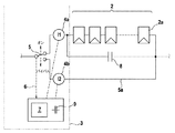
図1は、例示的な太陽光発電システム1を示している。これは、相互に接続されたサブモジュール2のアレイから成る。このサブモジュールはそれぞれ個々の太陽電池2aから形成されている。各個々の太陽電池内で、光起電作用によって生成された電圧は、接続によって合算される。従ってこの結果、各個々のサブモジュール2は、サブモジュールにかかる電圧を形成し、最終的に、全体的な太陽光発電システムにかかる総電圧に寄与する。
FIG. 1 shows an exemplary photovoltaic system 1. This consists of an array of
個々のサブモジュールは、この構成において、最小機能単位として機能し、制御回路3によって駆動制御される。制御回路は、個々のサブモジュールによって生成される電気的なソーラー電流の電流強度を監視する。1つまたは複数のサブモジュール内で、ソーラー電流の電流強度が、殊に、暗化によって、特定の値を下回ると、相応のサブモジュールが制御回路によってバイパスされる。これによって、その内部抵抗が、太陽光発電システム全体に悪影響を及ぼさない。 In this configuration, each submodule functions as a minimum functional unit and is driven and controlled by the control circuit 3. The control circuit monitors the current intensity of the electrical solar current generated by the individual submodules. In one or more submodules, if the current intensity of the solar current falls below a certain value, in particular due to darkening, the corresponding submodule is bypassed by the control circuit. Thereby, the internal resistance does not adversely affect the entire photovoltaic power generation system.
以下では、制御回路の作用を、サブモジュールと、当該サブモジュールのための制御回路とから成る装置に基づいて説明する。複数のサブモジュールから構成されている太陽光発電システムの場合には、各個々のサブモジュールに1つの固有の制御回路が割り当てられるか、または目的に応じて、複数のサブモジュールが1つの制御回路と接続されてもよい。 In the following, the operation of the control circuit will be described based on a device comprising a submodule and a control circuit for the submodule. In the case of a photovoltaic power generation system composed of a plurality of submodules, one individual control circuit is assigned to each individual submodule, or a plurality of submodules are one control circuit depending on the purpose. May be connected.
図2は、第1の例示的な実施形態の、制御回路3を備えたサブモジュール2の回路図の例示的な図を示している。ここに示されているサブモジュールは、複数の個々の太陽電池2aから成る。制御回路は、電流測定器4aおよび4bを備えている電流測定装置4と、切り替えパルス6が加えられる切り替えスイッチ5と、タイマーユニット7と含んでいる。
FIG. 2 shows an exemplary diagram of a circuit diagram of a
切り替えスイッチ5は、サブモジュールの結合および分離に用いられる。これはオンスイッチング状態またはバイパススイッチング状態を取る。オンスイッチング状態では、サブモジュールは太陽光発電システムのシステム全体を形成するように接続されている。太陽光発電システム内のシステム電流はこの場合には、サブモジュールの太陽電池2a内を流れる。これは、ソーラー電流の自身の部分に寄与する。バイパススイッチング状態では、サブモジュールはバイパスされ、これによって、太陽光発電システムの回路から離される。全体的な電流の流れはこの場合には、サブモジュールをバイパスしている電流経路5aを介して導かれる。
The changeover switch 5 is used for coupling and separation of submodules. This takes an on switching state or a bypass switching state. In the on-switching state, the submodules are connected to form the entire system of the photovoltaic system. In this case, the system current in the photovoltaic power generation system flows in the
この装置によって形成されるないしはこの装置を流れるソーラー電流は、電流測定装置4によって検出される。ここで第1の電流測定器4aは、オンスイッチング状態の間に、サブモジュールによって生成される電流強度I1を測定し、第2の電流測定器4aはバイパススイッチング状態の間に、太陽光発電システム全体内で生成される電流強度I2を測定する。両方の値は、ここには図示されていないサンプル&ホールド回路内で相互に比較される。
The solar current formed by or flowing through this device is detected by the current measuring device 4. Here, the first
タイマーユニット7は、切り替えスイッチ5に切り替えパルス6を加える。このような場合は、切り替えスイッチ5のスイッチング状態は、オンスイッチング状態からバイパススイッチング状態へと切り替えられる、またはバイパススイッチング状態からオンスイッチング状態へと戻される。サブモジュールはこれによってバイパスされて、太陽光発電システムのシステム全体から切り離されるか、または、太陽光発電システムの回路内に組み込まれる。
The
この切り替え過程は、コンデンサ8によって影響される。このコンデンサは、サブモジュール2に対して並列接続されており、サブモジュールの作動中に充電される。サブモジュールの暗化時に、コンデンサ8の放電が行われる。電流測定器4aに記録される電流強度I1は、これによって、コンデンサの放電電流によって生じる時定数で低下する。従って電流強度I1は、所定の遅延後に、所定の閾値を下回る。従ってコンデンサ8は、オンスイッチング状態からバイパススイッチング状態への切り替えスイッチの遅延した切り替えを生じさせる。
This switching process is affected by the capacitor 8. This capacitor is connected in parallel to the
ここで重要なのは、この切り替え過程の遅延が、コンデンサの充電状態およびサブモジュール2の性能に依存している、ということである。サブモジュール2の短時間のみの暗化または弱い暗化の場合には、コンデンサ8は比較的大きい時定数を伴う放電電流を出力する。従って、電流強度I1は、比較的長い時間幅の後にはじめて、所定の閾値を下回る。このような場合には、バイパススイッチング状態への切り替えは、大きい遅延を伴って用いられるか、または阻止される。これによって、弱く暗化されているだけのサブモジュールは、回路全体から切り離されない。この場合にはコンデンサは、一時的なエネルギー蓄積部として作用する。
What is important here is that the delay of this switching process depends on the state of charge of the capacitor and the performance of the
強い暗化の場合、殊に、サブモジュールの完全な暗化の場合には、コンデンサの放電は、比較的小さい時定数で行われる。従ってコンデンサは迅速に放電され、電流強度I1は、これによって相応に迅速に所定の閾値を下回り、バイパススイッチング状態への切り替えが、比較的短い時間間隔の後に行われる。これによって、完全に暗化され、エネルギー生成に使用されていないサブモジュールが迅速にバイパスされる。 In the case of strong darkening, in particular in the case of complete darkening of the submodule, the capacitor discharge takes place with a relatively small time constant. The capacitor is thus quickly discharged, and the current intensity I1 is thereby correspondingly quickly below the predetermined threshold, and the switching to the bypass switching state takes place after a relatively short time interval. This quickly bypasses sub-modules that are completely darkened and not used for energy generation.
オンスイッチング状態への再切り替えは、タイマーユニットの新たな切り替えパルスによって行われる。 Switching back to the on-switching state is performed by a new switching pulse of the timer unit.
このためにタイマーユニットは、タイミングサイクルを有している。これは、バイパススイッチング状態への切り替え後に、オンスイッチング状態への切り替えスイッチの周期的な切り替えを生じさせる。図2に示されている実施例では、さらに、タイマーコンデンサ9が設けられている。これは、自身の放電によって、新たな切り替えパルスの生起、ひいてはオンスイッチング状態とバイパススイッチング状態との間での切り替えスイッチ5の交互の切り替えをトリガする。
For this purpose, the timer unit has a timing cycle. This results in periodic switching of the switch to the on-switching state after switching to the bypass switching state. In the embodiment shown in FIG. 2, a
サブモジュールまたは太陽光発電システムによってタイマーコンデンサが給電される場合には、そのトリガ機能が直接的に、サブモジュールまたは太陽光発電システムの目下のエネルギー生成と結合される。これによって、太陽光発電システムまたはサブモジュールのソーラー電流から導出された時間に従って、切り替えスイッチは、それぞれ別の位置に切り替えられる。 When the timer capacitor is powered by the submodule or photovoltaic system, its trigger function is directly coupled to the current energy generation of the submodule or photovoltaic system. Thereby, according to the time derived | led-out from the solar current of a photovoltaic power generation system or a submodule, a changeover switch is each switched to another position.
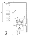
図3は、別の例示的な実施例における、制御回路3を備えたサブモジュール2を示している。この例では、制御回路がモノリシックに組み込まれている。制御回路は、さらに、組み込まれたタイマーユニット7を有している。電流強度I1およびI2を測定するために、この例では2つのスイッチングトランジスタが設けられている。各スイッチングトランジスタで得られる、ドレインとソースとの間の順抵抗はここで、回路ロジックに対する測定用分岐回路11として作用する。この測定用分岐回路は、2つの分岐回路11aと11bとから成る。分岐回路のオーム抵抗を介して、それぞれ降下する電圧V1およびV2は、各オンスイッチング状態ないしはバイパススイッチング状態において問い合わせされ、電流強度値I1およびI2に換算される。ここでこのタイマーは、内部で設定されている切り替え時点、ひいては新たな測定のためのタイミングサイクルを設定する。この例でも、サブモジュールはコンデンサ8によって緩衝され、記載されているように、バイパス状態へのサブモジュールの移行を、コンデンサの放電によって定められる遅延時点で行う。
FIG. 3 shows a
図4は、ソーラー電流生成の制御の例示的なフローチャートを示している。これは、相互に噛み合っている2つの、ループ状の方法フローを含んでいる。 FIG. 4 shows an exemplary flowchart of solar current generation control. This includes two, loop-like method flows that are interdigitated.
第1の方法フローは、太陽光発電システム内の継続的な目標値更新に関する。これは、リセットステップ12で始まる。ここでは、切り替え信号が切り替えスイッチに出力される。切り替えスイッチは、さらに、切り替えステップ13において、バイパススイッチング状態に切り替えられる。次に、システム電流12に対する値がステップ14において測定され、ステップ15において制御回路のサンプル&ホールド(S/H)段において記憶される。サンプル&ホールド段は、内部の蓄積器の形態で、または、例えば組み込み容量を介したアナログ電圧として形成される。
The first method flow relates to continuous target value update in the photovoltaic power generation system. This begins with
第2の方法フローは、サブモジュールによって生成された電流強度I1の継続的な測定と、ここで特定された値とシステム電流I2に対する、サンプル&ホールド段内に記憶されている値との継続的な比較とによって形成されている。このために、切り替え過程16が行われ、ここで、切り替えスイッチは、オンスイッチング状態に切り替えられる。その後、測定ステップ17において、サブモジュールによって生成された電流強度I1が測定される。同時に、この電流強度I1が、値12または相応に値I2から導出された閾値を下回っているか否かが検査される。
The second method flow is a continuous measurement of the current intensity I1 generated by the sub-module and the value identified here and the value stored in the sample and hold stage for the system current I2. It is formed by simple comparison. For this purpose, a
タイマーユニットは、ここで、固定された切り替えサイクルTで、オンスイッチング状態とバイパススイッチング状態との交互の切り替えを生じさせる。従って、上述した2つの方法フローが交互に実施される。この交互の切り替えは有利には次のように設計されている。すなわち、セットパルスが切り替えスイッチをバイパススイッチング位置に切り替え、後続のリセットパルスが切り替えスイッチを再び、オンスイッチング状態にセットし、これによって、リセットパルスの後は、切り替えスイッチが常にオンスイッチング状態にあるように設計されている。 The timer unit now causes alternating switching between the on switching state and the bypass switching state in a fixed switching cycle T. Accordingly, the two method flows described above are performed alternately. This alternating switching is advantageously designed as follows. That is, the set pulse switches the changeover switch to the bypass switching position, and the subsequent reset pulse sets the changeover switch again to the on switching state, so that after the reset pulse, the changeover switch is always in the on switching state. Designed to.
ここで、オンスイッチング状態はいつでも中断可能である。これは次のような場合である。すなわち、測定ステップ17に続く判断ステップ18が、電流強度I1が、値I2によって設定された、または値I2から導かれた目標値を下回っていることを伝えるとすぐにこのようなケースになる。ここで切り替えスイッチはバイパススイッチング状態へ、ステップ13を新たに実施することによって切り替えられ、サブモジュールが電流回路から分断される。このサブモジュールは、その後、自立して作動し、コンデンサ8を、サブモジュール内で継続して生成されるソーラーエネルギーによって再び充電する。
Here, the on-switching state can be interrupted at any time. This is the case as follows. That is, this is the case as soon as the
このバイパススイッチング状態は遅くとも、タイマーユニットが新たな切り替えパルスを切り替えスイッチに出力し、リセットステップ12およびこれに続く、ステップ16、17および18が再び実施されると、再び終了する。
Even if this bypass switching state is late, the timer unit outputs a new switching pulse to the changeover switch, and when the
図5は、ソーラー電流生成の制御中の例示的な切り替え過程の図を、時間ダイヤグラムに基づいて示している。このダイヤグラムは、一方では、タイマーユニット7によって出力される、一連の切り替えパルスT1、T2およびT3を示している。これらは、切り替えサイクルT内で順次連続している。その下に、電流強度I1の時間的な経過特性が示されている。
FIG. 5 shows a diagram of an exemplary switching process during control of solar current generation based on a time diagram. This diagram shows on the one hand a series of switching pulses T1, T2 and T3 output by the
第1の切り替えパルスT1の間、電流I1は、システム電流I2に対応している。第2のリセットパルスの時点T2で、暗化が生じる。これによって、サブモジュールの電流は例えば、システム電流の70%まで低下する。電流I1は、時点tI1<Thresholdで、ここに示されている、例えば電流I2の80%の閾値IThresholdを下回る。この下回りによって、切り替えパルスUがトリガされる。この時点から、サブモジュールがバイパスされる。サブモジュールにおいて実行され続けているソーラー電流生成は、コンデンサ8を、再び、破線ILに沿って充電する。第3のリセットパルスT3の時点で、切り替えスイッチは、再び、オンスイッチング状態にセットされ、コンデンサは再び放電する。この場合には、サブモジュールの暗化は、まだ克服されていないので、新たな切り替えパルスUがトリガされ、上述の過程が繰り返される。ここでこのバイパスされているサブモジュール内で継続して電流が生成され、コンデンサ内に集められ、時点T1およびT2の後、システムに出力される。 During the first switching pulse T1, the current I1 corresponds to the system current I2. Darkening occurs at time T2 of the second reset pulse. As a result, the current of the submodule is reduced to, for example, 70% of the system current. Current I1 at time t I1 <Threshold, shown here, for example, below 80% of the threshold I Threshold current I2. This lowering triggers the switching pulse U. From this point on, the submodule is bypassed. Solar current generation continues to be executed in the sub-module, a capacitor 8, again, is charged along broken line I L. At the time of the third reset pulse T3, the changeover switch is again set to the ON switching state, and the capacitor is discharged again. In this case, since the darkening of the submodule has not yet been overcome, a new switching pulse U is triggered and the above process is repeated. Here, current is continuously generated in this bypassed submodule, collected in a capacitor, and output to the system after times T1 and T2.
図6は、暗化の度合に依存している、例示的な切り替え特性の図を、ダイヤグラムに基づいて示している。サブモジュールによって生成されたソーラーエネルギーが、明らかに、システム全体のソーラーエネルギーを下回っている場合(これは強い暗化の場合である)には、サブモジュール電流I1が極めて迅速に、システム電流I2によって定められている値IThresholdを下回り、切り替えスイッチは既に時点t1でバイパススイッチング状態に切り替えられる。これに対して、弱い暗化のみが存在する場合には、コンデンサは、高い終値のために、格段に緩慢に放電する。従って、スイッチは格段に遅く、時点t2またはt3で、バイパススイッチング状態に切り替えられる。これによってこのサブモジュールは、エネルギー生成全体に甚大に寄与する。 FIG. 6 shows a diagram of an exemplary switching characteristic, depending on the degree of darkening, based on the diagram. If the solar energy generated by the submodule is clearly below the total system solar energy (this is the case for strong darkening), the submodule current I1 is very quickly increased by the system current I2. lower than the are defined value I Threshold, the changeover switch is switched to the already bypass switching state at time t 1. On the other hand, if only weak darkening is present, the capacitor discharges much more slowly due to the high closing price. Therefore, the switch is much slower and is switched to the bypass switching state at time t 2 or t 3 . This submodule thus contributes significantly to the overall energy generation.
しかしタイマーユニットの時間制御、すなわち、タイミングサイクルTを可変にし、かつサブモジュールの動作とフィードバック結合させることができる。この場合にはまずは固定のタイミングサイクルTが可変にされ、リセットパルスがより迅速にまたはより緩慢に順次連続する。この時間制御は有利にはサブモジュール自身によって設定され、暗化が増すとともに、すなわち電流I1の低下に依存して、より短い時間へとシフトするように調整される。 However, the time control of the timer unit, that is, the timing cycle T can be made variable and can be feedback-coupled to the operation of the submodule. In this case, the fixed timing cycle T is first made variable, and the reset pulses are successively continued more quickly or more slowly. This time control is advantageously set by the submodule itself and is adjusted to shift to shorter times as the darkening increases, i.e. depending on the decrease in the current I1.
このような構成は、システム全体内に、それぞれに割り当てられている切り替え装置を伴って直列接続されている複数のサブモジュールが、1つよりも多い切り替えサイクルにわたって相互に影響されない、という利点を提供する。すなわち2つまたはそれよりも多くの切り替え装置が同時にバイパススイッチング状態に移行し、これによって論理的に、極端な場合には、全てのサブモジュールがバイパスされ得るという可能性を無視することできる。 Such a configuration offers the advantage that multiple submodules connected in series with a switching device assigned to each in the entire system are not affected by one another over more than one switching cycle. To do. That is, the possibility that two or more switching devices simultaneously enter the bypass switching state, thereby logically neglecting the possibility that all sub-modules can be bypassed.
別の利点は、太陽光入射が少ない場合には、サブモジュールの内在しているコンデンサとしてのセル容量も僅かになり、これによって、ソーラー電流が低くなると、コンデンサが迅速に放電され、再充電される、ということである。 Another advantage is that when the sunlight incident is low, the cell capacity of the submodule's internal capacitor is also small, so that when the solar current is low, the capacitor is quickly discharged and recharged. That is.
別の構成では、太陽電池2aの内在している容量が利用される。ダイオード容量としても公知の、pn接合部のこの容量は照射に依存しており、240cm2の面積の高性能太陽電池の場合には、照射されていない場合には10μFまでの値が得られ、完全な照射(1000W/m2)の場合には1000μFの値が得られる。この容量はそれぞれ、太陽電池である電流源に並列接続されているので、近似的に、サブストリングの全体容量を同じオーダーに設定することができる。これによって、有利な実施形態では、例えば図2に示されている別個の外部コンデンサを省くことができる。
In another configuration, the capacity inherent in the
効率を最適化するために基本的に、切り替えパルスひいてはそれぞれ別の比較電流の測定は、極めて短い時間のみを必要とする。これは明らかである。なぜなら、暗化されていないサブモジュールの場合には、比較に必要な測定(ひいてはサブモジュールの短絡)によって、得られる成果が引き下げられてしまうからである。しかし、完全照射時に、切り替えのための100μsの測定時間(完全放射時および100mOhmのRDSonにおける、極めて高く設定された、1000μFのコンデンササイズの場合)および1sのホールド時間(次のリセットまでの時間)を仮定した場合には、100ppmまたは0.01%の効果損失が生じる。さらに、図3に示された測定用分岐回路を介した損失も考慮されなければならない。8Aの定格電流の場合には、これによって、800mWがエネルギースイッチを介して降下し、従って、240Wの定格出力を有するモジュールあたり3つのエネルギースイッチを設けると、3×24mW=72mWの出力損失がリセットパルスによって生じ、3×800mW=2.4Wの出力損失が直列接続されたパワートランジスタによって生じ、全体では、サブモジュールあたり約3Wの出力損失が生じる。 In order to optimize the efficiency, basically the measurement of the switching pulse and thus the respective comparison current requires only a very short time. This is clear. This is because, in the case of sub-modules that are not darkened, the results obtained are reduced by the measurement required for comparison (and consequently the short-circuit of the sub-modules). However, completely irradiated during, 100 [mu] s of the measurement time for switching (at full radiation and during 100mOhm of R DSon, set very high, if the capacitor size of 1000 pF) and 1s hold time (time until the next reset ), An effect loss of 100 ppm or 0.01% occurs. Furthermore, the losses through the measuring branch circuit shown in FIG. 3 must also be taken into account. For a rated current of 8A, this causes 800mW to drop through the energy switch, so providing 3 energy switches per module with a rated output of 240W resets the output loss of 3 x 24mW = 72mW Due to the pulse, an output loss of 3 × 800 mW = 2.4 W is caused by the power transistors connected in series, and overall, an output loss of about 3 W per submodule occurs.
太陽照射が少ない場合には、セル容量がファクター100だけ低減する。従って、156mmの太陽電池の場合に、約10μFのセル容量が予期される。これによって、測定時間は1μsまで短くなる。しかしこの場合には有利には短いリセットインターバルに基づいて、効率損失も同様にシフトする。ここで有利な想定は1msであり、暗化されていない動作時には依然として、99.9%の効果が得られ、同様に約1%の、パワートランジスタによる比較的小さい損失が差し引かれる。 When solar irradiation is low, the cell capacity is reduced by a factor of 100. Thus, for a 156 mm solar cell, a cell capacity of about 10 μF is expected. This shortens the measurement time to 1 μs. In this case, however, the efficiency loss shifts as well, preferably based on a short reset interval. An advantageous assumption here is 1 ms, and still 99.9% of the effect is obtained during non-darkened operation, as well as a relatively small loss of about 1% due to the power transistor.
すなわち近似的に、本願に記載されている装置の使用並びに方法の実施形態によって、ソーラー電流の約1%を、暗化されていない状態で損失する。しかしこれは、暗化時の比例的なゲインと対向している。これに必要な回路技術的なコストは格段に、DC/DC変換器が組み込まれている既知のモジュールベースのMPPTを下回る。 That is, approximately 1% of the solar current is lost undarkened by the use of the apparatus and method embodiments described herein. However, this is opposed to the proportional gain during darkening. The circuit technical costs required for this are far below those of known module-based MPPTs that incorporate DC / DC converters.
性能見積りのために、例えば、16Aの最大の順方向電流時および16Aの最大スイッチング電圧時に、ドレインとソースの間で、100mOhmのオーム抵抗RDSonを有するパワートランジスタ(FET)を想定する。例えば、10mOhmにこのスイッチオン抵抗を最適化することによって、出力損失は、例えば0.32ワット弱まで低減され、これによって格段に0.2%を下回る。換言すれば:ここに示された方法は、暗化されていないサブモジュールの出力と比較して、99.8%の効率を保証する。しかしこの低い性能損失は、暗化時のサブモジュールの効果的な電力出力と対向する。 For performance estimates, for example, at the maximum of the maximum switching voltage of forward current time and 16A of 16A, between the drain and the source, assuming the power transistor (FET) with an ohmic resistance R DSon of 100 mohms. For example, by optimizing this switch-on resistance to 10 mOhm, the output loss is reduced to, for example, less than 0.32 watts, thereby far below 0.2%. In other words: the method shown here guarantees an efficiency of 99.8% compared to the output of the non-darkened submodule. However, this low performance loss is opposed to the effective power output of the submodule during darkening.
切り替えスイッチを強制的にバイパススイッチング位置に移行させるコミュニケーションインタフェースを使用することによって、このサブモジュールおよび全体的な太陽光発電システムは無電流状態、むしろモジュールの短絡状態に切り替えられる。このようなスイッチング状態を、以降で、「使用不能状態」と称す。これは、例えば必要なモジュール交換中に、サブモジュールが日中の間、切り離されなければならない場合、または例えば火災の場合に、例えば炎を消す目的で屋根を開けるために、システムが無電流に切り替えられなければならない場合に有利である。 By using a communication interface that forces the changeover switch to the bypass switching position, the sub-module and the overall photovoltaic system are switched to the no-current state, rather the module short-circuit state. Such a switching state is hereinafter referred to as “unusable state”. This means that the system can be switched to no-current, for example during a necessary module change, when a sub-module has to be disconnected during the day, or in the event of a fire, for example to open the roof in order to extinguish flames. This is advantageous when it has to be done.
コミュニケーションの可能なアプローチはここで、別個の制御線路である。この制御線路は全てのサブモジュールに接続されている。同様に、パワーラインコンセプトが利用可能であり、ここでは信号が、ソーラー電流線路を介して送られる。または既知の高周波コミュニケーションプロトコール(Zigbee、W−LAN等)を介した無線のアプローチが利用される。パワーラインコンセプトが利用される場合には、例えば、「使用可能」信号の印加が、通常の、図3に示されているモジュールの動作様式に対して必ず必要になる。ここで、この使用可能信号の伝送には完全なソーラー電流線路が必要である。故障時にライトアークが生じると、この際に生じるイネーブル信号のノイズスペクトルが妨害となり、コミュニケーションユニットはこの信号を識別しなくなり、「使用不能」モードに切り替えられる。従って、ライトアークの識別および、ライトアークが消えるまで電流回路内で電圧がシフトダウンされることによる(サブモジュールの「切り離し」による)自動除去が実現されるだろう。 A possible approach for communication here is a separate control line. This control line is connected to all the submodules. Similarly, a power line concept is available, where the signal is sent via a solar current line. Alternatively, a wireless approach via a known high-frequency communication protocol (Zigbee, W-LAN, etc.) is used. Where the power line concept is utilized, for example, the application of an “enabled” signal is necessarily required for the normal mode of operation of the module shown in FIG. Here, a complete solar current line is required for the transmission of this usable signal. If a light arc occurs in the event of a failure, the noise spectrum of the enable signal generated at this time will be disturbed and the communication unit will not recognize this signal and will be switched to the “unavailable” mode. Thus, light arc identification and automatic removal by shifting down the voltage in the current circuit (by “disconnecting” the submodule) will be realized until the light arc disappears.
専門家の行為の範囲内で、本願に単に例として示された方法および装置の発展的な構成および実施形態が得られる。発展的な実施形態は、従属請求項に記載されている。 Within the scope of professional action, advanced configurations and embodiments of the method and apparatus, which are presented here by way of example only, are obtained. Advanced embodiments are set forth in the dependent claims.
Claims (14)
前記太陽光発電システムは、当該太陽光発電システムを形成するように接続されている少なくとも1つのサブモジュールを有している、方法において、
切り替えタイミングサイクル(T)で、オンスイッチング状態とバイパススイッチング状態との間で前記サブモジュールを交互に切り替え、前記サブモジュールは、前記オンスイッチング状態において前記太陽光発電システムに接続されており、前記バイパススイッチング状態においてバイパスされており、
・前記バイパススイッチング状態の間に前記太陽光発電システムの総電流強度(I2)を測定し、前記総電流強度(I2)から求められた目標値(IThreshold)を一時記憶し、前記オンスイッチング状態の間にサブモジュール電流強度(I1)を測定し、前記目標値と比較し、
・前記サブモジュール電流強度(I1)が前記目標値を下回ると、前記切り替えタイミングサイクル(T)に依存しないで、前記サブモジュールを前記バイパススイッチング状態にリセット(Z)する、
ことを特徴とする、太陽光発電システム内の電流生成を制御するための方法。 A method for controlling current generation in a photovoltaic system, comprising:
The photovoltaic system comprises at least one submodule connected to form the photovoltaic system,
In the switching timing cycle (T), the submodule is alternately switched between an on switching state and a bypass switching state, and the submodule is connected to the photovoltaic power generation system in the on switching state, and the bypass Bypassed in switching state,
The total current intensity (I2) of the photovoltaic power generation system is measured during the bypass switching state, the target value ( IThreshold ) obtained from the total current intensity (I2) is temporarily stored, and the on-switching state During this period, the sub-module current intensity (I1) is measured and compared with the target value.
If the sub-module current intensity (I1) falls below the target value, the sub-module is reset (Z) to the bypass switching state without depending on the switching timing cycle (T);
A method for controlling current generation in a photovoltaic system.
前記太陽光発電システムは、当該太陽光発電システムを形成するように接続されている少なくとも1つのサブモジュールを有しており、
前記装置は、
前記サブモジュール(2)によって生成された電流強度を測定する第1の電流測定装置(4a)と、前記太陽光発電システム内で生成された電流強度を測定する第2の電流測定装置(4b)とを備えた制御回路(3)と、
前記サブモジュールが前記太陽光発電システムに接続されているオンスイッチング状態、または、前記サブモジュールがバイパスされているバイパススイッチング状態に前記サブモジュールをセットする切り替えスイッチ(5)と、
当該切り替えスイッチを調整するタイマーユニット(7)とを有し、
前記制御回路(3)は、
・前記バイパススイッチング状態の間に前記太陽光発電システムの総電流強度(I2)を測定し、前記総電流強度(I2)から求められた目標値(I Threshold )を一時記憶し、前記オンスイッチング状態の間にサブモジュール電流強度(I1)を測定し、前記目標値と比較し、
・前記サブモジュール電流強度(I1)が前記目標値を下回ると、前記切り替えタイミングサイクル(T)に依存しないで、前記サブモジュールを前記バイパススイッチング状態にリセット(Z)する、
ことを特徴とする、太陽光発電システム内の電流生成を制御するための装置。 A device for controlling current generation in a photovoltaic system,
The solar power system has at least one sub-module connected to form the solar power system,
The device is
A first current measuring device (4a) for measuring the current intensity generated by the submodule (2), and a second current measuring device (4b) for measuring the current intensity generated in the solar power generation system. A control circuit (3) comprising:
The on-switching state submodule is connected to the photovoltaic power generation system, or a selector switch for setting said sub-module into a bypass switching state in which the sub-module is bypassed (5),
Possess a timer unit (7) for adjusting the selector switch,
The control circuit (3)
The total current intensity (I2) of the photovoltaic power generation system is measured during the bypass switching state, the target value ( IThreshold ) obtained from the total current intensity (I2 ) is temporarily stored, and the on-switching state During this period, the sub-module current intensity (I1) is measured and compared with the target value.
If the sub-module current intensity (I1) falls below the target value, the sub-module is reset (Z) to the bypass switching state without depending on the switching timing cycle (T);
An apparatus for controlling current generation in a photovoltaic system.
Applications Claiming Priority (3)
| Application Number | Priority Date | Filing Date | Title |
|---|---|---|---|
| DE102010029813.1 | 2010-06-08 | ||
| DE102010029813.1A DE102010029813B4 (en) | 2010-06-08 | 2010-06-08 | Method for controlling electrical power generation of a sub-module in a photovoltaic system |
| PCT/EP2011/055983 WO2011154185A1 (en) | 2010-06-08 | 2011-04-15 | Method and device for controlling the electricity generation of a sub-module in a photovoltaic system |
Publications (2)
| Publication Number | Publication Date |
|---|---|
| JP2013535095A JP2013535095A (en) | 2013-09-09 |
| JP5490317B2 true JP5490317B2 (en) | 2014-05-14 |
Family
ID=44625955
Family Applications (1)
| Application Number | Title | Priority Date | Filing Date |
|---|---|---|---|
| JP2013513594A Active JP5490317B2 (en) | 2010-06-08 | 2011-04-15 | Method and apparatus for controlling current generation of submodules in a photovoltaic system |
Country Status (8)
| Country | Link |
|---|---|
| US (1) | US20130154394A1 (en) |
| EP (1) | EP2580843B1 (en) |
| JP (1) | JP5490317B2 (en) |
| KR (1) | KR20130089154A (en) |
| CN (1) | CN102918746B (en) |
| DE (1) | DE102010029813B4 (en) |
| TW (1) | TW201206045A (en) |
| WO (1) | WO2011154185A1 (en) |
Families Citing this family (8)
| Publication number | Priority date | Publication date | Assignee | Title |
|---|---|---|---|---|
| DE102011082160A1 (en) * | 2011-09-06 | 2013-03-07 | Robert Bosch Gmbh | Protective switching device, photovoltaic system and method for operating such |
| WO2014011392A2 (en) * | 2012-07-09 | 2014-01-16 | Dow Global Technologies Llc | Systems and methods for detecting discontinuities in a solar array circuit and terminating current flow therein |
| WO2014085468A1 (en) * | 2012-11-29 | 2014-06-05 | Dow Global Technologies Llc | Systems and methods for reducing electric potential in photovoltaic systems |
| DE102013202600B4 (en) * | 2013-02-19 | 2015-04-16 | Siemens Aktiengesellschaft | Method for yield optimization of a partially shaded photovoltaic field |
| DE102013217727A1 (en) | 2013-09-05 | 2015-03-05 | Robert Bosch Gmbh | Device comprising at least one photovoltaic cell and solar module with improved overall efficiency and method for operating such a device and such a solar module |
| KR101937338B1 (en) * | 2014-03-03 | 2019-01-10 | 솔라리틱스, 인크. | Method and system for applying electric fields to multiple solar panels |
| US20200035853A1 (en) * | 2018-07-30 | 2020-01-30 | mPower Technology, Inc. | In-Situ Rapid Annealing and Operation of Solar Cells for Extreme Environment Applications |
| CN112769132B (en) * | 2021-01-06 | 2022-08-12 | 华南理工大学 | Converter valve state and valve current solving method based on valve side current time sequence characteristics |
Family Cites Families (9)
| Publication number | Priority date | Publication date | Assignee | Title |
|---|---|---|---|---|
| DE19916742C1 (en) * | 1999-04-13 | 2000-08-24 | Angew Solarenergie Ase Gmbh | Solar cell current generation circuit has bypass diodes across each solar cell chain connected in series and bridged in groups by further diodes |
| US7342440B2 (en) * | 2005-03-04 | 2008-03-11 | Infineon Technologies Austria Ag | Current regulator having a transistor and a measuring resistor |
| DE102005021152B4 (en) * | 2005-05-02 | 2007-03-08 | Universität Stuttgart | solar cell device |
| US8933321B2 (en) * | 2009-02-05 | 2015-01-13 | Tigo Energy, Inc. | Systems and methods for an enhanced watchdog in solar module installations |
| ITVA20080002A1 (en) | 2008-01-10 | 2009-07-11 | St Microelectronics Srl | PHOTOVOLTAIC SYSTEM WITH MULTICELLULAR PANELS WITH MULTIPLATE DC-DC CONVERSION FOR CELL GROUPS IN SERIES OF EACH PANEL AND PHOTOVOLTAIC PANEL STRUCTURE |
| DE102008008504A1 (en) * | 2008-02-11 | 2009-08-13 | Siemens Aktiengesellschaft | Method for theft detection of a PV module and failure detection of a bypass diode of a PV module as well as corresponding PV sub-generator junction box, PV inverter and corresponding PV system |
| US8273979B2 (en) * | 2008-10-15 | 2012-09-25 | Xandex, Inc. | Time averaged modulated diode apparatus for photovoltaic application |
| DE102009051186A1 (en) | 2008-10-29 | 2010-05-06 | Fraunhofer-Gesellschaft zur Förderung der angewandten Forschung e.V. | Matching circuit for use in solar generator, has controller controlling switching device, where controller is designed in such manner that direct current/direct current converter is taken into account during timing loss |
| WO2010071877A2 (en) * | 2008-12-21 | 2010-06-24 | Navsemi, Inc. | System and method for selectively controlling a solar panel in segments |
-
2010
- 2010-06-08 DE DE102010029813.1A patent/DE102010029813B4/en active Active
-
2011
- 2011-04-15 JP JP2013513594A patent/JP5490317B2/en active Active
- 2011-04-15 CN CN201180028207.4A patent/CN102918746B/en active Active
- 2011-04-15 WO PCT/EP2011/055983 patent/WO2011154185A1/en active Application Filing
- 2011-04-15 KR KR20127032163A patent/KR20130089154A/en not_active Application Discontinuation
- 2011-04-15 US US13/702,960 patent/US20130154394A1/en not_active Abandoned
- 2011-04-15 EP EP11715911.1A patent/EP2580843B1/en active Active
- 2011-06-07 TW TW100119782A patent/TW201206045A/en unknown
Also Published As
| Publication number | Publication date |
|---|---|
| US20130154394A1 (en) | 2013-06-20 |
| KR20130089154A (en) | 2013-08-09 |
| CN102918746A (en) | 2013-02-06 |
| EP2580843B1 (en) | 2017-05-10 |
| TW201206045A (en) | 2012-02-01 |
| DE102010029813A1 (en) | 2011-12-08 |
| DE102010029813B4 (en) | 2023-02-23 |
| EP2580843A1 (en) | 2013-04-17 |
| JP2013535095A (en) | 2013-09-09 |
| WO2011154185A1 (en) | 2011-12-15 |
| CN102918746B (en) | 2016-02-17 |
Similar Documents
| Publication | Publication Date | Title |
|---|---|---|
| JP5490317B2 (en) | Method and apparatus for controlling current generation of submodules in a photovoltaic system | |
| JP7095962B2 (en) | Safety switch for photovoltaic system | |
| US11114862B2 (en) | Localized power point optimizer for solar cell installations | |
| US8212409B2 (en) | Method for activating a multi-string inverter for photovoltaic plants | |
| EP3410551B1 (en) | System for interconnected elements of a power system | |
| CN108604607B (en) | Protection circuit for a Photovoltaic (PV) module, method for operating the protection circuit and Photovoltaic (PV) system comprising such a protection circuit | |
| CN105958934B (en) | Power optimizer | |
| TW201013361A (en) | System and method for integrating local maximum power point tracking into an energy generating system having centralized maximum power point tracking | |
| CN105915156B (en) | Photovoltaic power generation system with power optimizer | |
| US20220382313A1 (en) | Systems and methods for quick dissipation of stored energy from input capacitors of power inverters | |
| CN109066847B (en) | Photovoltaic power generation charge-discharge control circuit | |
| CA2624035C (en) | Solar module | |
| US20210351741A1 (en) | Safety Switch for Photovoltaic Systems | |
| CN105978476B (en) | Inverter | |
| KR101671078B1 (en) | Maximum power point tracking apparatus and method | |
| CN104854528A (en) | Systems and methods for controlling maximum power point tracking controllers | |
| EP3291309A1 (en) | Safety switch for photovoltaic systems | |
| CN111435796B (en) | Safety switch for photovoltaic system | |
| CN113067473B (en) | Control signal modulation circuit, inverter and control system | |
| EP3925051B1 (en) | Device for coupling a solar panel to an inverter and a system formed thereby | |
| CN114123735A (en) | Series-parallel converter protection system, controller and converter |
Legal Events
| Date | Code | Title | Description |
|---|---|---|---|
| A977 | Report on retrieval |
Free format text: JAPANESE INTERMEDIATE CODE: A971007 Effective date: 20131218 |
|
| TRDD | Decision of grant or rejection written | ||
| A01 | Written decision to grant a patent or to grant a registration (utility model) |
Free format text: JAPANESE INTERMEDIATE CODE: A01 Effective date: 20140127 |
|
| A61 | First payment of annual fees (during grant procedure) |
Free format text: JAPANESE INTERMEDIATE CODE: A61 Effective date: 20140225 |
|
| R150 | Certificate of patent or registration of utility model |
Ref document number: 5490317 Country of ref document: JP Free format text: JAPANESE INTERMEDIATE CODE: R150 |
|
| R250 | Receipt of annual fees |
Free format text: JAPANESE INTERMEDIATE CODE: R250 |
|
| S111 | Request for change of ownership or part of ownership |
Free format text: JAPANESE INTERMEDIATE CODE: R313113 |
|
| R350 | Written notification of registration of transfer |
Free format text: JAPANESE INTERMEDIATE CODE: R350 |
|
| R250 | Receipt of annual fees |
Free format text: JAPANESE INTERMEDIATE CODE: R250 |
|
| R250 | Receipt of annual fees |
Free format text: JAPANESE INTERMEDIATE CODE: R250 |
|
| R250 | Receipt of annual fees |
Free format text: JAPANESE INTERMEDIATE CODE: R250 |
|
| R250 | Receipt of annual fees |
Free format text: JAPANESE INTERMEDIATE CODE: R250 |
|
| R250 | Receipt of annual fees |
Free format text: JAPANESE INTERMEDIATE CODE: R250 |
|
| R250 | Receipt of annual fees |
Free format text: JAPANESE INTERMEDIATE CODE: R250 |
|
| R250 | Receipt of annual fees |
Free format text: JAPANESE INTERMEDIATE CODE: R250 |